

Page 1
PRODUCT PREVIEW
Please be aware that an important notice concerning availability, standard warranty, and use in critical applications of Texas Instruments
查询ADS1610IPAPR供应商
ANALOG-TO-DIGITAL CONVERTER
¨
ADS1610
SBAS344A − AUGUST 2005 − REVISED SEPTEMBER 2005
16-Bit, 10MSPS
FEATURES
D High-Speed, Wide Bandwidth ∆Σ ADC
D 10MSPS Output Data Rate
D 4.9MHz Signal Bandwidth
D 86dBFS Signal-to-Noise Ratio
D −94dB Total Harmonic Distortion
D 95dB Spurious-Free Dynamic Range
D On-Chip Digital Filter Simplifies Anti-Alias
Requirements
D SYNC Pin for Simultaneous Sampling with
Multiple ADS1610s
D Low 3µs Group Delay
D Parallel Interface
D Directly Connects to TMS320 DSPs
D Out-of-Range Alert Pin
D Pin-Compatible with ADS1605 (5MSPS ADC)
APPLICATIONS
D Scientific Instruments
D Test Equipment
D Communications
VREFP
VREFN
DESCRIPTION
The ADS1610 is a high-speed, high-precision, deltasigma (∆Σ) analog-to-digital converter (ADC) with 16-bit
resolution operating from a +5V analog and a +3V digital
supply. Featuring an advanced multi-stage analog
modulator combined with an on-chip digital decimation
filter, the ADS1610 achieves 86dBFS signal-to-noise ratio
(SNR) in a 5MHz signal bandwidth. The device offers
outstanding performance at these speeds with a total
harmonic distortion of −94dB.
The ADS1610 ∆Σ topology provides key system-level
design advantages with respect to anti-alias filtering and
clock jitter. The design of the anti-alias filter is simplified
since the on-chip digital filter greatly attenuates
out-of-band signals. The ADS1601s filter has a brick wall
response with a very flat passband (±0.0002dB of ripple)
followed immediately by a very wide stop band (5MHz to
55MHz). Clock jitter becomes especially critical when
digitizing high frequency, large-amplitude signals. The
ADS1610 significantly reduces clock jitter sensitivity by an
effective averaging of clock jitter as a result of
oversampling the input signal.
Output data is supplied over a parallel interface and easily
connects to TMS320 digital signal processors (DSPs).
The power dissipation can be adjusted with an external
resistor, allowing for reduction at lower operating speeds.
With its outstanding high-speed performance, the
ADS1610 is well-suited for demanding applications in data
acquisition, scientific instruments, test and measurement
equipment, and communications. The ADS1610 is offered
in a TQFP-64 package and is specified from −40°C to
+85°C.
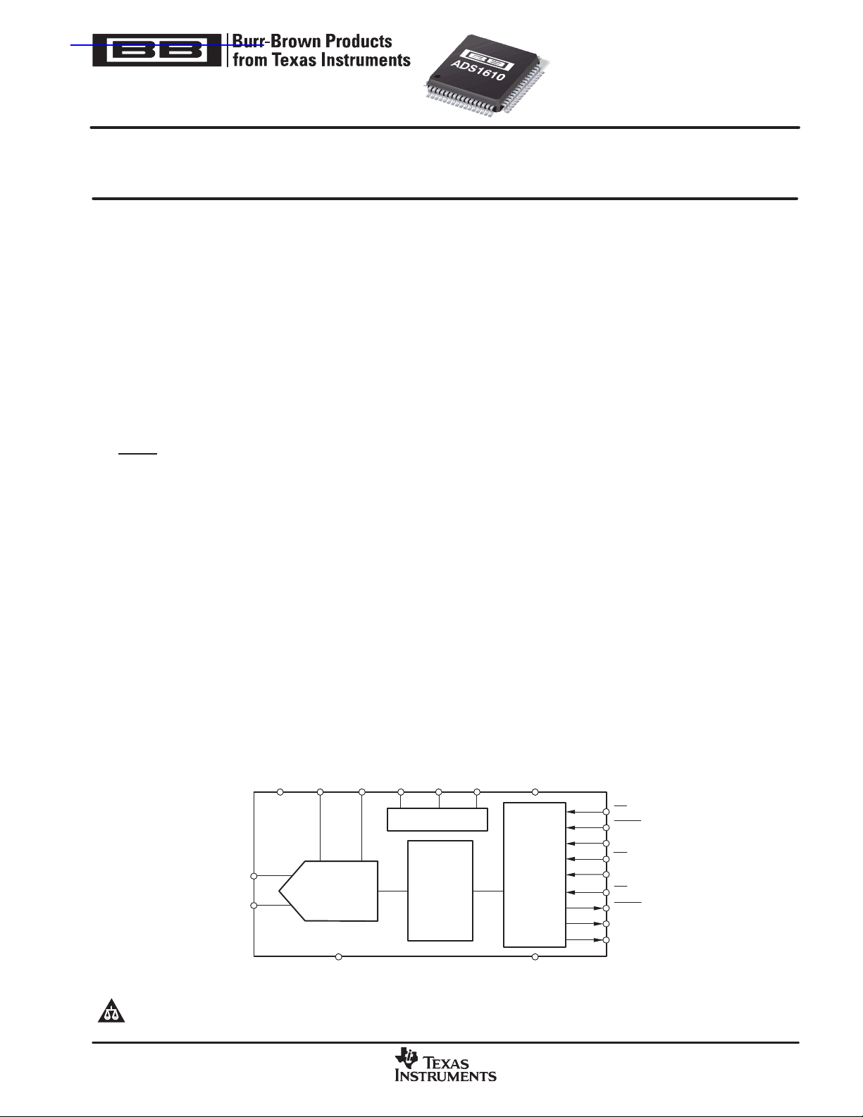
VMID RBIAS VCAPAVDD
DVDD
Bias Circuits
AINP
AINN
ADS1610
semiconductor products and disclaimers thereto appears at the end of this data sheet.
PowerPAD is a registered trademark of Texas Instruments. All other trademarks are the property of their respective owners.
!
∆Σ
Modulator
AGND DGND
Digital
Filter
www.ti.com
Parallel
Interface
PD
SYNC
CLK
CS
2xMODE
RD
DRDY
OTR
DOUT[15:0]
Copyright 2005, Texas Instruments Incorporated
Page 2
"#$%$&
PRODUCT PREVIEW
SBAS344A − AUGUST 2005 − REVISED SEPTEMBER 2005
www.ti.com
ABSOLUTE MAXIMUM RATINGS
over operat i n g f ree-air temperature range unless otherwise noted
ADS1610 UNIT
AVDD to AGND −0.3 to +6 V
DVDD to DGND −0.3 to +3.6 V
AGND to DGND −0.3 to +0.3 V
Input Current 100mA, Momentary
Input Current 10mA, Continuous
Analog I/O to AGND −0.3 to AVDD + 0.3 V
Digital I/O to DGND −0.3 to DVDD + 0.3 V
Maximum Junction Temperature +150 °C
Operating Temperature Range −40 to +105 °C
Storage Temperature Range −60 to +150 °C
Lead Tem perature (soldering, 10s) +260 °C
(1)
Stresses above these ratings may cause permanent damage.
Exposure to absolute maximum conditions for extended periods
may degrade device reliability. These are stress ratings only , an d
functional operation of the device at these or any other conditions
beyond those specified is not implied.
(1)
PACKAGE/ORDERING INFORMATION
For the most current package and ordering information,
see the Package Option Addendum at the end of this
document, or see the TI website at www.ti.com.
This integrated circuit can be damaged by ESD. Texas
Instruments recommends that all integrated circuits be
handled with appropriate precautions. Failure to observe
proper handling and installation procedures can cause damage.
ESD damage can range from subtle performance degradation to
complete device failure. Precision integrated circuits may be more
susceptible t o damage because very small parametric changes could
cause the device not to meet its published specifications.
2
Page 3
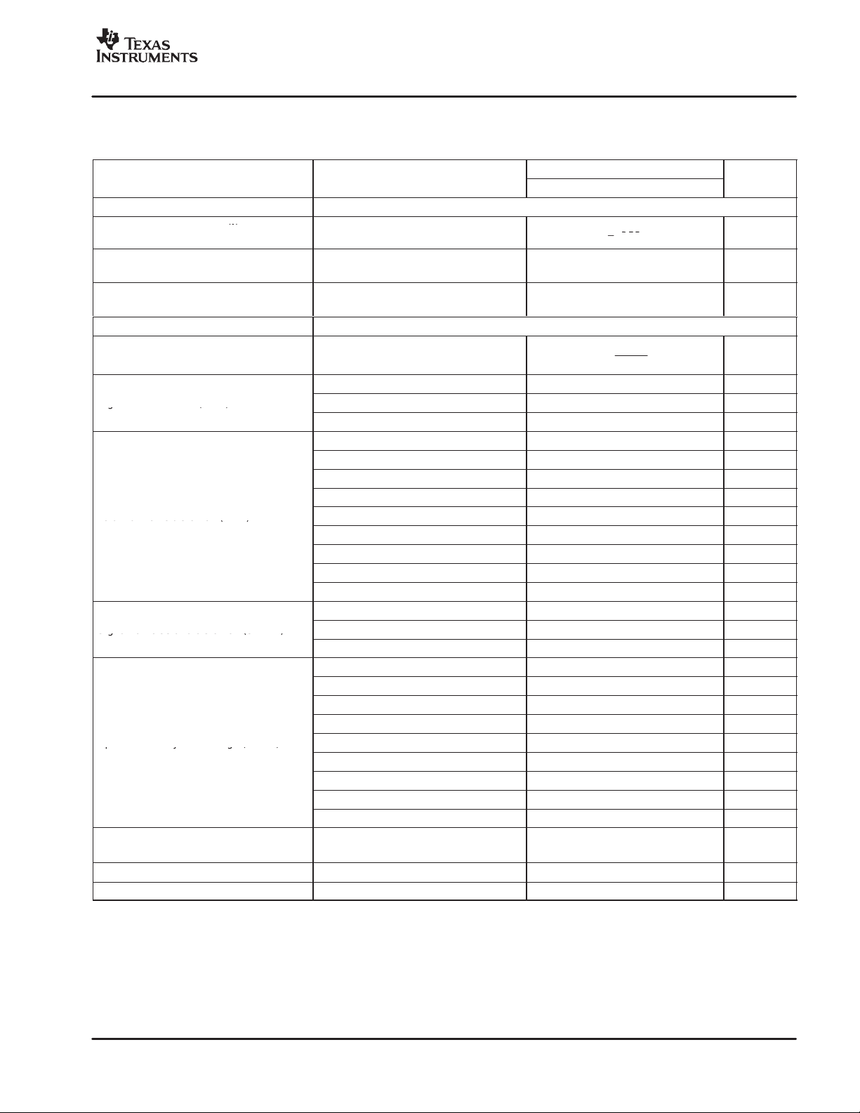
www.ti.com
Differential input voltage (VIN)
Differential input voltage (VIN)
V
REF
V
(AINP − AINN)
±V
REF
V
Signal-to-noise ratio (SNR)
Total harmonic distortion (THD)
Signal-to-noise and distortion (SINAD)
Spurious-free dynamic range (SFDR)
Intermodulation distortion
f1 = 3.8MHz, −8dBFS
TBD
dB
PRODUCT PREVIEW
ELECTRICAL CHARACTERISTICS
All specifications at −40°C to +85°C, AVDD = 5V, DVDD = 3V, f
unless otherwise noted.
PARAMETER TEST CONDITIONS MIN TYP MAX UNIT
Analog Input
= 60MHz, V
CLK
SBAS344A − AUGUST 2005 − REVISED SEPTEMBER 2005
= +3V, 2xMODE = low, VCM = 2.5V , and RBIAS = 18kΩ,
REF
ADS1610
±
"#$%$&
Common-mode input voltage (VCM)
(AINP + AINN)/2
Absolute input voltage
(AINP or AINN with respect to AGND)
Dynamic Specifications
Data rate
Signal-to-noise ratio (SNR)
Total harmonic distortion (THD)
Signal-to-noise and distortion (SINAD)
Spurious-free dynamic range (SFDR)
Aperture jitter Excludes jitter of CLK source 2 ps, rms
Aperture delay 4 ns
2.5 V
−0.1 4.2 V
f
CLK
ǒ
60MHz
Ǔ
10
f
= 100kHz, −2dBFS 86 dBFS
SIG
f
= 1MHz, −2dBFS 85 dBFS
SIG
f
= 4MHz, −2dBFS 85 dBFS
SIG
f
= 100kHz, −2dBFS −90 dB
SIG
f
= 100kHz, −6dBFS −95 dB
SIG
f
= 100kHz, −20dBFS −95 dB
SIG
f
= 1MHz, −2dBFS −89 dB
SIG
f
= 1MHz, −6dBFS −93 dB
SIG
f
= 1MHz, −20dBFS −95 dB
SIG
f
= 4MHz, −2dBFS −109 dB
SIG
f
= 4MHz, −6dBFS −105 dB
SIG
f
= 4MHz, −20dBFS −95 dB
SIG
f
= 100kHz, −2dBFS 85 dBFS
SIG
f
= 1MHz, −2dBFS 84 dBFS
SIG
f
= 4MHz, −2dBFS 85 dBFS
SIG
f
= 100kHz, −2dBFS 90 dB
SIG
f
= 100kHz, −6dBFS 96 dB
SIG
f
= 100kHz, −20dBFS 96 dB
SIG
f
= 1MHz, −2dBFS 91 dB
SIG
f
= 1MHz, −6dBFS 93 dB
SIG
f
= 1MHz, −20dBFS 96 dB
SIG
f
= 4MHz, −2dBFS 109 dB
SIG
f
= 4MHz, −6dBFS 105 dB
SIG
f
= 4MHz, −20dBFS 95 dB
SIG
f1 = 3.8MHz, −8dBFS
f2 = 4MHz, −8dBFS
MSPS
3
Page 4
"#$%$&
Passband transition
PRODUCT PREVIEW
www.ti.com
SBAS344A − AUGUST 2005 − REVISED SEPTEMBER 2005
ELECTRICAL CHARACTERISTICS (continued)
All specifications at −40°C to +85°C, AVDD = 5V, DVDD = 3V, f
unless otherwise noted.
PARAMETER UNITMAXTYPMINTEST CONDITIONS
Digital Filter Characteristics
Passband 0
Passband ripple ±0.0002 dB
−0.1dB attenuation
−3.0dB attenuation
Stop band
Stop band attenuation 80 (see Figure 14) dB
= 60MHz, V
CLK
= +3V, 2xMODE = low, VCM = 2.5V , and RBIAS = 18kΩ,
REF
ADS1610
f
CLK
ǒ
60MHz
Ǔ
4.4
f
CLK
ǒ
60MHz
ǒ
60MHz
f
CLK
Ǔ
Ǔ
4.6
4.9
5.6 54.4
MHz
MHz
MHz
MHz
Group delay
Settling time To ±0.001% 5.5 µs
Static Specifications
Resolution No missing codes 16 Bits
Input referred noise TBD µV, rms
Integral nonlinearity End-point fit, −2dBFS signal ±0.75 LSB
Differential nonlinearity ±0.5 LSB
Offset error T = +25°C TBD mV
Offset drift TBD µV//°C
Gain error T = +25°C TBD %
Gain drift Excluding reference drift TBD ppm/°C
Common-mode rejection At DC TBD dB
Power-supply rejection At DC TBD dB
Voltage Reference
(VREFP − VREFN)
V
REF
VREFP 3.6 4.0 4.4 V
VREFN 0.9 1.0 1.1 V
VMID 2.2 2.5 3.8 V
Digital Input/Output
V
IH
V
IL
V
OH
V
OL
Input leakage DGND < V
Power-Supply Requirements
AVDD 4.9 5.0 5.1 V
DVDD 2.7 3.0 3.6 V
AVDD current 150 mA
DVDD current 70 mA
Power dissipation 960 mW
60MHz
ǒ
f
Ǔ
CLK
3.0
2.9 3.0 3.1 V
0.7 DVDD DVDD V
DGND 0.3 DVDD V
IOH = −50µA 0.8 DVDD V
IOL = 50µA 0.2 DVDD V
DIGITAL INPUT
< DVDD ±10 µA
µs
4
Page 5
"#$%$&
PRODUCT PREVIEW
www.ti.com
SBAS344A − AUGUST 2005 − REVISED SEPTEMBER 2005
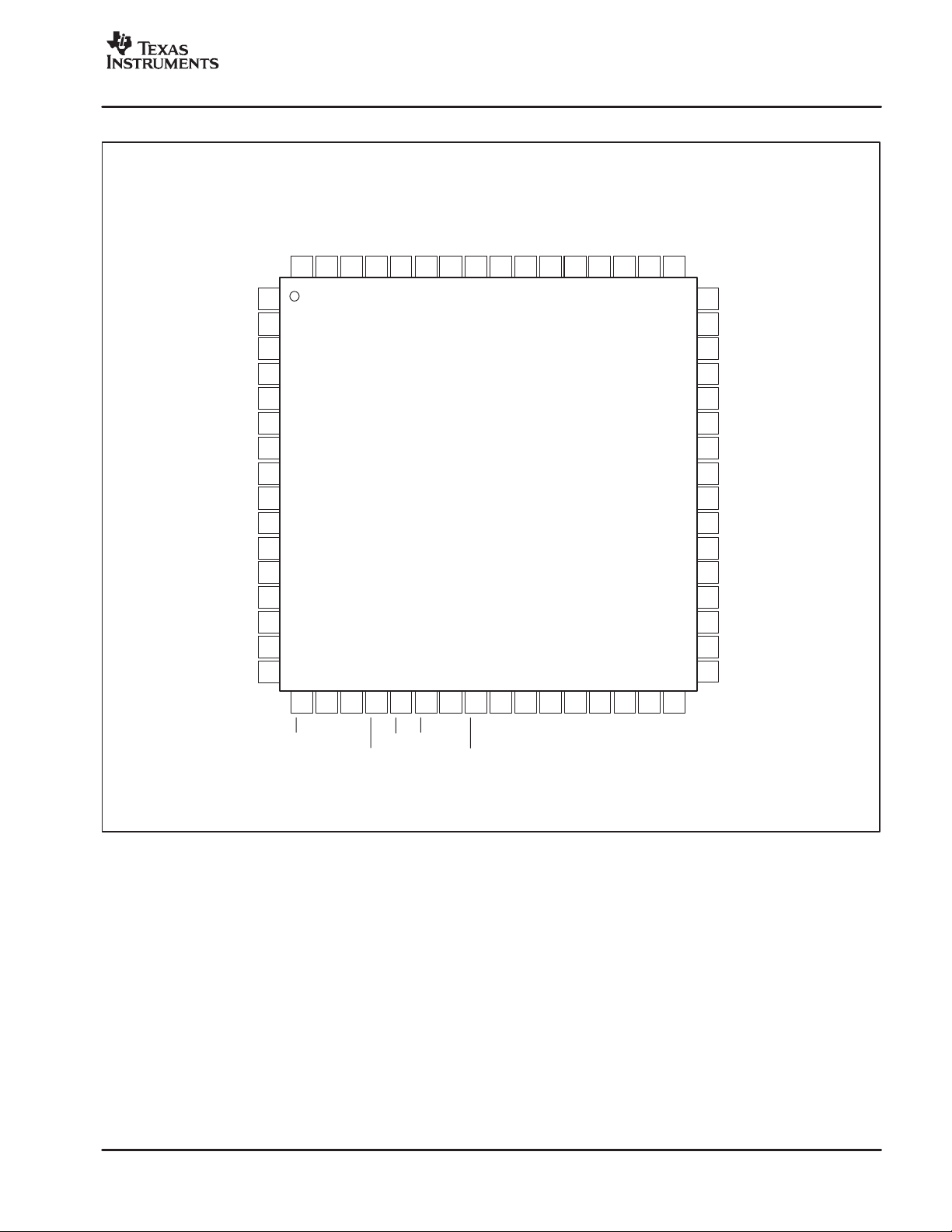
PIN CONFIGURATION
Top View HTQFP
VREFP
VREFP
VMID
VREFN
VREFN
VCAP
AVDD2
AGND2
CLK
AGND
DGND
DVDD
DVDD
DGND
DVDD
DVDD
64 63 62 61 60 59 58 57 56 55 54
53 52 51 50 49
AGND
AVDD
AGND
AINN
AINP
AGND
AVDD
RBIAS
AGND
AVDD
AGND
AVDD
NC
2xMODE
NC
NC
1
2
3
4
5
6
7
8
9
10
11
12
13
14
15
16
17 18 19 20 21 22 23 24 25 26 27
PD
DVDD
DGND
SYNC
CS
ADS1610
RD
OTR
48
NC
47
NC
46
NC
45
NC
44
DOUT[15]
43
DOUT[14]
42
DOUT[13]
41
DOUT[12]
40
DOUT[11]
39
DOUT[10]
38
DOUT[9]
37
DOUT[8]
36
DOUT[7]
35
DOUT[6]
34
DOUT[5]
33
DOUT[4]
28 29 30 31 32
NC
DRDY
DGND
DVDD
NC
DOUT[0]
DOUT[1]
DOUT[2]
DOUT[3]
5
Page 6
"#$%$&
PRODUCT PREVIEW
www.ti.com
SBAS344A − AUGUST 2005 − REVISED SEPTEMBER 2005
PIN FUNCTION DESCRIPTION
ANALOG/DIGITAL
PIN NAME PIN #
AGND 1, 3, 6, 9, 11, 55 Analog Analog Ground
AVDD 2, 7, 10, 12 Analog Analog Supply
AINN 4 Analog Input Negative Analog Input
AINP 5 Analog Input Positive Analog Input
RBIAS 8 Analog Analog Bias Setting Resistor
NC 13, 15, 16, 27, 28, 45-48 — Must be left unconnected.
2xMODE 14 Digital Input; Active High 2xMODE (20MSPS)
PD 17 Digital Input; Active Low Power-Down
DVDD 18, 26, 49, 50, 52, 53 Digital Digital Supply
DGND 19, 25, 51, 54 Digital Digital Ground
SYNC 20 Digital Input; Active Low Digital Reset
CS 21 Digital Input; Active Low Chip-Select
RD 22 Digital Input; Active Low Read Enable
OTR 23 Digital Output Analog Inputs Out-Of-Range
DRDY 24 Digital Output Data Ready
DOUT[15:0] 29-44 Digital Output Data Output. DOUT[15] is the MSB and DOUT[0] is the LSB.
CLK 56 Digital Input Clock Input
AGND2 57 Analog Analog Ground for AVDD2
AVDD2 58 Analog Analog Supply for Modulator Clocking
VCAP 59 Analog Bypass Capacitor
VREFN 60, 61 Analog Negative Reference Voltage
VMID 62 Analog Midpoint Voltage
VREFP 63, 64 Analog Positive Reference Voltage
INPUT/OUTPUT
DESCRIPTION
6
Page 7
www.ti.com
PRODUCT PREVIEW
TIMING SPECIFICATIONS
t
1
CLK
t
3
"#$%$&
SBAS344A − AUGUST 2005 − REVISED SEPTEMBER 2005
t
2
t
2
DRDY
t
6
t
5
DOUT[15:0] Data N Data N + 1 Data N + 2
t
4
t
4
Figure 1. Data Retrieval Timing
CLK
RD, CS
DOUT[15:0]
t
7
t
8
Figure 2. DOUT Inactive/Active Timing
DRDY
SYNC
DOUT[15:0] Valid Data
t
11
t
9
t
10
Figure 3. Reset Timing
7
Page 8

"#$%$&
PRODUCT PREVIEW
www.ti.com
SBAS344A − AUGUST 2005 − REVISED SEPTEMBER 2005
Timing Specifications
SYMBOL DESCRIPTION MIN TYP MAX UNITS
t
1/t
t
t
t
t
t
t
t
t
t
10
t
11
(1)
Output load = 10pF 500kΩ.
CLK Period (1/f
1
f
1
CLK
CLK Pulse Width, High or Low TBD ns
2
CLK to DRDY High (propagation delay) 10 ns
3
DRDY Pulse Width, High or Low 4 t
4
Previous Data Valid (hold time) TBD ns
5
New Data Valid (setup time) TBD ns
6
First Rising Edge CLK After RD and/or CS Inactive (high) to DOUT High Impedance TBD ns
7
First Rising Edge CLK After RD and/or CS Active (low) to DOUT Active TBD ns
8
Delay from SYNC Active (low) to All-Zero DOUT[15:0] TBD ns
9
Delay from SYNC Inactive (high) to Non-Zero DOUT[15:0] TBD ns
Delay from Non-Zero DOUT[15:0] to Valid DOUT[15:0]
(time − 55 DRDY cycles; required for digital filter to settle).
) TBD 16.667 ns
CLK
60 TBD MHz
1
5.5 µs
ns
8
Page 9

www.ti.com
PRODUCT PREVIEW
TYPICAL CHARACTERISTICS
At TA = +25°C, R
= 18kΩ, AVDD = 5V, DVDD = 3V, f
BIAS
= 60MHz, V
CLK
SBAS344A − AUGUST 2005 − REVISED SEPTEMBER 2005
= 3V , and VCM = 2.5V , unless otherwise noted.
REF
"#$%$&
0
−
20
−
40
−
60
−
80
−
100
Amplitude (dB)
−
120
−
140
−
160
0 1.5 2.0 2.5 3.0 3.5 4.0 4.50.5 1.0 5.0
0
−
20
−
40
−
60
−
80
−
100
Amplitude (dB)
−
120
−
140
−
160
0 1.5 2.0 2.5 3.0 3.5 4.0 4.50.5 1.0 5.0
SPECTRAL RESPONSE
fIN=100kHz,−2dBFS
Frequency (MHz)
SPECTRAL RESPONSE
fIN=1.0MHz,−2dBFS
Frequency (MHz)
SNR = 86dBFS
THD =−90dB
SFDR = 90dB
SNR = 86dBFS
THD =−91dB
SFDR = 94dB
0
−
20
−
40
−
60
−
80
−
100
Amplitude (dB)
−
120
−
140
−
160
0 1.5 2.0 2.5 3.0 3.5 4.0 4.50.5 1.0 5.0
0
−
20
−
40
−
60
−
80
−
100
Amplitude (dB)
−
120
−
140
−
160
0 1.5 2.0 2.5 3.0 3.5 4.0 4.50.5 1.0 5.0
SPECTRAL RESPONSE
fIN=100kHz,−6dBFS
Frequency (MHz)
SPECTRAL RESPONSE
fIN=1.0MHz,−6dBFS
Frequency (MHz)
SNR = 86dBFS
THD =−95dB
SFDR = 97dB
SNR = 86dBFS
THD =−93dB
SFDR = 94dB
0
Amplitude (dB)
fIN=4.0MHz,−2dBFS
SNR = 86dBFS
−
20
SFDR= 109dB
−
40
−
60
−
80
−
100
−
120
−
140
−
160
0 1.5 2.0 2.5 3.0 3.5 4.0 4.50.5 1.0 5.0
SPECTRAL RESPONSE
Frequency (MHz)
0
fIN=4.0MHz,−6dBFS
SNR = 86dBFS
−
20
SFDR= 105dB
−
40
−
60
−
80
−
100
Amplitude (dB)
−
120
−
140
−
160
0 1.5 2.0 2.5 3.0 3.5 4.0 4.50.5 1.0 5.0
SPECTRAL RESPONSE
Frequency (MHz)
9
Page 10

"#$%$&
PRODUCT PREVIEW
SBAS344A − AUGUST 2005 − REVISED SEPTEMBER 2005
TYPICAL CHARACTERISTICS (continued)
At TA = +25°C, R
= 18kΩ, AVDD = 5V, DVDD = 3V, f
BIAS
100
SNR, THD, SFDR (dB)
90
80
70
60
50
40
30
20
10
CLK
TOTAL HARMONIC DISTORTION,AND
SPURIOUS−FREE DYNAMIC RANGE vs INPUT
−
−
70
60−50 0
= 60MHz, V
SIGNAL−TO−NOISE RATIO,
SIGNAL AMPLITUDE
SFDR
−
Input Signal (dB)
= 3V , and VCM = 2.5V , unless otherwise noted.
REF
THD
SNR
40−30−20−10
www.ti.com
fIN=100kHz
10
Page 11

www.ti.com
PRODUCT PREVIEW
"#$%$&
SBAS344A − AUGUST 2005 − REVISED SEPTEMBER 2005
OVERVIEW
The ADS1610 is a high-performance, delta-sigma ADC.
The modulator uses an inherently stable, pipelined,
delta-sigma modulator architecture incorporating proprietary circuitry that allows for very linear high-speed
operation. The modulator samples the input signal at
60MSPS (when f
digital filter decimates the modulator output by 6 to provide
data output word rates of 10MSPS with a signal passband
out to 4.9MHz. The double speed mode, enabled by digital
I/O pin 2xMODE, doubles the data rate to 20MSPS by
reducing the oversampling ratio to 3. See the 2x Mode
section on page 19 for more detail.
Conceptually, the modulator and digital filter measure the
differential input signal, V
differential reference, V
shown in Figure 4. A 16-bit parallel data bus, designed for
direct connection to DSPs, outputs the data. A separate
power supply for the I/O allows flexibility for interfacing to
different logic families. Out-of-range conditions are
indicated with a dedicated digital output pin. Analog power
dissipation is controlled using an external resistor. This
allows reduced dissipation when operating at slower
speeds. When not in use, power consumption can be
dramatically reduced using the PD
= 60MHz). A low-ripple linear phase
CLK
= (AINP − AINN), against the
IN
= (VREFP − VREFN), as
REF
pin.
The ADS1610 supports a very wide range of input signals.
Having such a wide input range makes out-of-range
signals unlikely. However, should an out-of-range signal
occur, the digital output OTR will go high.
To achieve the highest analog performance, it is
recommended that the inputs be limited to 0.891V
(−1dBFS). For V
= 3V, the corresponding
REF
REF
recommended input range is ±2.67.
The analog inputs must be driven with a differential signal
to achieve optimum performance. The recommended
common-mode voltage of the input signal,
V
AINP) AINN
+
CM
2 , is 2.5V.
In addition to the differential and common-mode input
voltages, the absolute input voltage is also important. This
is the voltage on either input (AINP or AINN) with respect
to AGND. The range for this voltage is:
−0.1V t(AINN or AINP)t 4.2V
(1)
If either input is taken below −0.1V , ESD protection diodes
on the inputs will turn on. Exceeding 4.2V on either input
will result in linearity performance degradation. ESD
protection diodes will also turn on if the inputs are taken
above AVDD (+5V).
ANALOG INPUTS (AINP, AINN)
The ADS1610 measures the differential signal,
= (AINP − AINN), against the differential reference,
V
IN
V
= (VREFP − VREFN).
REF
AINP
AINN
VREFNVREFP
Σ
V
REF
V
IN
Σ
Σ∆
Modulator
Digital
Filter
Parallel
Interface
Figure 4. Conceptual Block Diagram
OTR
DOUT[15:0]
2xMODE
11
Page 12

"#$%$&
PRODUCT PREVIEW
SBAS344A − AUGUST 2005 − REVISED SEPTEMBER 2005
www.ti.com
INPUT CIRCUITRY
The ADS1610 uses switched-capacitor circuitry to
measure the input voltage. Internal capacitors are charged
by the inputs and then discharged internally with this cycle
repeating at the frequency of CLK. Figure 5 shows a
conceptual diagram of these circuits. Switches S
represent the net effect of the modulator circuitry in
discharging the sampling capacitors, the actual
implementation is different. The timing for switches S1 and
S
is shown in Figure 6.
2
ADS1610
8pF
VMID
8pF
VMID
S
2
S
2
AINP
AINN
AGND
S
1
10pF
S
1
10pF
Figure 7 and Figure 8 show the recommended circuits
when using single-ended or differential op amps,
respectively. The analog inputs must be driven
differentially to achieve optimum performance. If only a
single-ended input signal is available, the configuration in
Figure 8 can be used by shorting −VIN to ground.
2
This configuration would implement the single-ended to
differential conversion.
The external capacitors, between the inputs and from each
input to AGND, improve linearity and should be placed as
close to the pins as possible. Place the drivers close to the
inputs and use good capacitor bypass techniques on their
supplies; usually a smaller high-quality ceramic capacitor
in parallel with a larger capacitor. Keep the resistances
used in the driver circuits low-thermal noise in the driver
circuits degrades the overall noise performance. When the
signal can be AC-coupled to the ADS1610 inputs, a simple
RC filter can set the input common mode voltage. The
ADS1610 is a high-speed, high-performance ADC.
Special care must be taken when selecting the test
equipment and setup used with this device. Pay particular
attention to the signal sources to ensure they do not limit
performance when measuring the ADS1610.
Figure 5. Conceptual Diagram of Internal
Circuitry Connected to the Analog Inputs
t
=1/f
SAMPLE
On
S1
Off
On
S2
Off
Figure 6. Timing for the Switches in Figure 2
CLK
DRIVING THE INPUTS
The external circuits driving the ADS1610 inputs must be
able to handle the load presented by the switching
capacitors within the ADS1610. The input switches S1 in
Figure 5 are closed approximately one half of the sampling
period, t
capacitors to be charged by the inputs, when
f
= 60MHz.
CLK
, allowing only ∼8ns for the internal
SAMPLE
Ω
392
Ω
392
V
IN
−
2
Ω
392
(1)
V
CM
Ω 1k
Ω
392
V
IN
2
Ω
392
(1)
V
CM
Ω
(1) Recommended VCM=2.5V.
(2) Optional ac−coupling circuit provides common−mode input voltage.
(3) Increase to 390pFwhen f
40pF
OPA2822
1µF392
392
40pF
OPA2822
1µF392
0.01µF
Ω
V
CM
1k
0.01µF
≤
100kHz for improved SNR and THD.
IN
Ω
49.9
(2)
100pF
Ω
(2)
(1)
Ω
(2)
100pF
(2)
49.9
100pF
(3)
Ω
AGND
AINP
ADS1610
AINN
Figure 7. Recommended Driver Circuit Using the
OPA2822
12
Page 13

"#$%$&
PRODUCT PREVIEW
www.ti.com
SBAS344A − AUGUST 2005 − REVISED SEPTEMBER 2005
22pF
Ω
787
Ω
56.2
374
Ω
V
CM
Ω
402
787
22pF
Ω
V
IN
Figure 8. Recommended Single-Ended to Differential Conversion Circuit Using the THS4503 Differential
Amplifier
12.5
12.5
Ω
100pF
Ω
100pF
100pF
AINP
ADS1610THS4503
AINN
REFERENCE INPUTS (VREFN, VREFP, VMID)
The ADS1610 operates from an external voltage
reference. The reference voltage V
differential voltage between VREFN and VREFP:
V
= (VREFP − VREFN). VREFP and VREFN each
REF
use two pins, which should be shorted together. VMID
equals approximately 2.5V and is used by the modulator.
VCAP connects to an internal node and must also be
bypassed with an external capacitor.
The voltages applied to these pins must be within the
values specified in the Electrical Characteristics table.
Typically VREFP = 4V, VMID = 2.5V, and VREFN = 1V.
The external circuitry must be capable of providing both a
DC and a transient current. Figure 9 shows a simplified
diagram of the internal circuitry of the reference. As with
the input circuitry, switches S
shown in Figure 6.
S
VREFP
VREFP
VREFN
VREFN
1
Ω
S
1
is set by the
REF
and S2 open and close as
1
ADS1610
S
50pF300
2
Figure 10 shows the recommended circuitry for driving
these reference inputs. Keep the resistances used in the
buffer circuits low to prevent excessive thermal noise from
degrading performance. Layout of these circuits is critical,
make sure to follow good high-speed layout practices.
Place the buffers and especially the bypass capacitors as
close to the pins as possible.
Ω
392
0.001µF
ADS1610
VREFP
VREFP
0.1µF
VMID
0.1µF
VREFN
VREFN
VCAP
0.1µF
2.5V
OPA2822
4V
392Ω
0.001µF
22µF
OPA2822
Ω
392
0.001µF
OPA2822
1V
10µF
0.1µ F
22µF
10µF
22µF
10µF 0.1µF
Figure 9. Conceptual Circuitry for the Reference
Inputs
AGND
Figure 10. Recommended Reference Buffer
Circuit
13
Page 14

"#$%$&
ALLOWABLE
PRODUCT PREVIEW
SBAS344A − AUGUST 2005 − REVISED SEPTEMBER 2005
www.ti.com
CLOCK INPUT (CLK)
The ADS1610 uses an external clock signal to be applied
to the CLK input pin. The sampling of the modulator is
controlled by this clock signal. As with any high-speed data
converter, a high quality clock is essential for optimum
performance. Crystal clock oscillators are the
recommended CLK source; other sources, such as
frequency synthesizers are usually not adequate. Make
sure to avoid excess ringing on the CLK input; keeping the
trace as short as possible will help.
Measuring high-frequency, large-amplitude signals
requires tight control of clock jitter. The uncertainty during
sampling of the input from clock jitter limits the maximum
achievable SNR. This effect becomes more pronounced
with higher frequency and larger magnitude inputs.
Fortunately, the ADS1610 oversampling topology reduces
clock jitter sensitivity over that of Nyquist rate converters
like pipeline and successive approximation converters by
a factor of √6
In order to not limit the ADS1610 SNR performance, keep
the jitter on the clock source below the values shown in
Table 1. When measuring lower frequency and lower
amplitude inputs, more CLK jitter can be tolerated. In
determining the allowable clock source jitter, select the
worst-case input (highest frequency, largest amplitude)
that will be seen in the application.
.
Table 2. Output Code Versus Input Signal
INPUT SIGNAL
(INP – INN)
≥ +V
−V
v −V
(1)
Excludes effects of noise, INL, offset and gain errors.
(> 0dB) 7FFF
REF
V
(0dB) 7FFF
REF
)V
REF
215* 1
0 0000
−V
REF
215* 1
15
2
REF
ǒ
REF
215* 1
15
2
ǒ
215* 1
Ǔ
Ǔ
IDEAL OUTPUT
CODE
0001
FFFF
8000
8000
(1)
H
H
H
H
H
H
H
OTR
1
0
0
0
0
0
1
Likewise, when the input is negative out-of-range by going
below the negative full-scale value of V
, the output clips
REF
to 8000h and the OTR output goes high. The OTR remains
high while the input signal is out-of-range.
DATA FORMAT
The 16-bit output data is in binary two’s complement
format, as shown in Table 2. When the input is positive
out-of-range, exceeding the positive full-scale value of
V
, the output clips to all 7FFFH and the OTR output goes
REF
high.
Table 1. Maximum Allowable Clock Source Jitter
for Different Input Signal Frequencies and
Amplitude
INPUT SIGNAL
MAXIMUM
FREQUENCY
4MHz −1dB 1.6ps
4MHz −20dB 14ps
2MHz −1dB 3.3ps
2MHz −20dB 29ps
1MHz −1dB 6.5ps
1MHz −20dB 58ps
100kHz −1dB 65ps
100kHz −20dB 581ps
MAXIMUM
AMPLITUDE
MAXIMUM
CLOCK SOURCE
JITTER
14
Page 15

www.ti.com
PRODUCT PREVIEW
OUT-OF-RANGE INDICATION (OTR)
If the output code on DOUT[15:0] exceeds the positive or
negative full-scale, the out-of-range digital output (OTR)
will go high on the falling edge of DRDY
code returns within the full-scale range, OTR returns low
on the falling edge of DRDY.
. When the output
SBAS344A − AUGUST 2005 − REVISED SEPTEMBER 2005
DRDY
outputs updating simultaneously. After
synchronization, allow 55 DRDY
cycles (t12) for output
data to fully settle.
"#$%$&
DATA RETRIEVAL
Data retrieval is controlled through a simple parallel
interface. The falling edge of the DRDY
output indicates
new data is available. T o activate the output bus, both CS
and RD must be low, as shown in Table 3. Make sure the
DOUT bus does not drive heavy loads (> 20pF), as this will
degrade performance. Use an external buffer when driving
an edge connector or cables.
Table 3. Truth Table for CS and RD
CS RD DOUT[15:0]
0 0 Active
0 1 High impedance
1 0 High impedance
1 1 High impedance
RESETTING THE ADS1610
The ADS1610 is asynchronously reset when the SYNC
pin is taken low. During reset, all of the digital circuits are
cleared, DOUT[15:0] are forced low, and DRDY
high. It is recommended that the SYNC
the falling edge of CLK. Afterwards, DRDY
pin be released on
goes low on the
second rising edge of CLK. Allow 55 DRDY
digital filter to settle before retrieving data. See Figure 3 for
the timing specifications.
forced
cycles for the
CLK
SYNC
DRDY
DOUT[15:0]
DRDY
DOUT[15:0]
SYNC
Clock
1
1
2
2
SYNC
CLK
SYNC
CLK
ADS1610
DOUT[15:0]
ADS1610
DOUT[15:0]
1
DRDY
2
DRDY
DRDY
DOUT[15:0]
DRDY
DOUT[15:0]
t
12
Synchronized
1
1
2
2
Settled
Data
Settled
Data
Reset can be used to synchronize multiple ADS1610s. All
devices to be synchronized must use a common CLK
input. With the CLK inputs running, pulse SYNC
falling edge of CLK, as shown in Figure 1 1. Afterwards, the
converters will be converting synchronously with the
on the
Figure 11. Synchronizing Multiple Converters
15
Page 16

"#$%$&
PRODUCT PREVIEW
SBAS344A − AUGUST 2005 − REVISED SEPTEMBER 2005
www.ti.com
SETTLING TIME
The settling time is an important consideration when
measuring signals with large steps or when using a
multiplexer in front of the analog inputs. The ADS1610
digital filter requires time for an instantaneous change in
signal level to propagate to the output.
Be sure to allow the filter time to settle after applying a large
step in the input signal, switching the channel on a
multiplexer placed in front of the inputs, resetting the
ADS1610, or exiting the power-down mode.
Figure 12 shows the settling error as a function of time for
a full-scale signal step applied at t = 0, with 2xMODE = low.
This figure uses DRDY
scale (X-axis). After 55 DRDY
drops below 0.001%. For f
to a settling time of 5.5µs.
1
10
0
10
−
1
10
−
2
10
−3
10
SettlingError (%)
−4
10
cycles for the ADS1610 for the time
cycles, the settling error
= 60MHz, this corresponds
CLK
1.0
0.8
0.6
0.4
0.2
0
Normalized Response
−
0.2
−
0.4
0 102030405060
Time (DRDY cycles)
Figure 13. Impulse Response
FREQUENCY RESPONSE
The linear phase FIR digital filter sets the overall frequency
response. The decimation rate is set to 6 (2xMODE = low)
for all the figures shown in this section. Figure 14 shows
the frequency response from DC to 30MHz for
f
= 60MHz. The frequency response of the ADS1610
CLK
filter scales directly with CLK frequency. For example, if
the CLK frequency is decreased by half (to 30MHz), the
values on the X-axis in Figure 14 would need to be scaled
by half, with the span becoming DC to 15MHz.
−5
10
30 35 40 45 50 55
Settling Time (DRDY cycle s)
Figure 12. Settling Time
IMPULSE RESPONSE
Figure 13 plots the normalized response for an input
applied at t = 0, with 2xMODE = low. The X-axis units of
time are DRDY
cycles for the ADS1610. As shown in
Figure 13, the peak of the impulse takes 30 DRDY
to propagate to the output. For f
cycle is 0.1µs in duration and the propagation time (or
group delay) is 30 × 0.1µs = 3.0µs.
= 60MHz, a DRDY
CLK
60
cycles
0
−
20
−
40
−
60
−
80
Magnitude(dB)
−
100
−
120
0105152520
Frequency (MHz)
Figure 14. Frequency Response
30
16
Page 17

www.ti.com
PRODUCT PREVIEW
"#$%$&
SBAS344A − AUGUST 2005 − REVISED SEPTEMBER 2005
Figure 15 shows the passband ripple from DC to 4.4MHz
= 60MHz). Figure 16 shows a closer view of the
(f
CLK
passband transition by plotting the response from 4.0MHz
to 5.0MHz (f
0.00020
0.00015
0.00010
0.00005
−0.000 05
Magnitude (dB)
−0.000 10
−0.000 15
−0.000 20
= 60MHz).
CLK
0
00.51.0
1.5 2.0 2.5 3.0 3.5 4. 0 4.5
Frequency (MHz)
Figure 15. Passband Ripple
0
−
1
−
2
−
3
−
4
Magnitude (dB)
−
5
−
6
−
7
4.0 4.24.1 4.3 4.5 4.7 4.94.4
Frequency (MHz)
4.6 4.8 5.0
0
−
20
−
40
−
60
−
80
Magnitude (dB)
−
100
−
120
02040
60 80 180100 120 140 160
Frequency (MHz)
Figure 17. Frequency Response Out to 120MHz
ANALOG POWER DISSIPATION
An external resistor connected between the RBIAS pin
and the analog ground sets the analog current level, as
shown in Figure 18. The current is inversely proportional
to the resistor value. Table 4 shows the recommended
values of RBIAS for different CLK frequencies. Notice that
the analog current can be reduced when using a slower
frequency CLK input because the modulator has more
time to settle. Avoid adding any capacitance in parallel to
RBIAS, since this will interfere with the internal circuitry
used to set the biasing.
ADS1610
RBIAS
RBIAS
Figure 16. Passband Transition
The overall frequency response repeats at multiples of the
CLK frequency. To help illustrate this, Figure 17 shows the
response out to 180MHz (f
CLK
passband response repeats at 60MHz, 120MHz, and
180MHz; it is important to consider this sequence when
there is high-frequency noise present with the signal. The
modulator bandwidth extends to 100MHz. High-frequency
noise around 60MHz and 120MHz will not be attenuated
by either the modulator or the digital filter. This noise will
alias back in; band and reduce the overall SNR
performance unless it is filtered out prior to the ADS1610.
To prevent this, place an anti-alias filter in front of the
ADS1610 that rolls off before 55MHz.
= 60MHz). Notice how the
AGND
Figure 18. External Resistor Used to Set Analog
Power Dissipation
Table 4. Recommended RBIAS Resistor Values
for Different CLK Frequencies
DATA
f
CLK
42MHz 7MHz TBD TBD
48MHz 8MHz TBD TBD
54MHz 9MHz TBD TBD
60MHz 10MHz 18kΩ 960mW
RATE
RBIAS
TYPICAL POWER
DISSIPATION
17
Page 18

"#$%$&
PRODUCT PREVIEW
SBAS344A − AUGUST 2005 − REVISED SEPTEMBER 2005
www.ti.com
POWER-DOWN (PD)
When not in use, the ADS1610 can be powered down by
taking the PD
including the voltage reference. To minimize the digital
current during power down, stop the clock signal supplied
to the CLK input. There is an internal pull-up resistor of
170kΩ on the PD
be connected to DVDD if not used. Make sure to allow time
for the reference to start up after exiting the power-down
mode. The internal reference typically requires 15µs. After
the reference has stabilized, allow at least 100 DRDY
cycles for the modulator and digital filter to settle before
retrieving data.
DVDD
AVDD
pin low. All circuitry will be shutdown,
pin, but it is recommended that this pin
47µF4.7µF1µF0.1µF
47µF
4.7µF
1µF
If using separate analog and
digital ground planes, connect
togetheron the ADS1610 PCB.
DGND
0.1µF
AGND
Ω
10
1
(1)
C
P
2
3
6
(1)
C
P
7
POWER SUPPLIES
Two supplies are used on the ADS1610: analog (AVDD),
and digital (DVDD). Each supply (other than DVDD pins 49
and 50) must be suitably bypassed to achieve the best
performance. It is recommended that a 1µF and 0.1µF
ceramic capacitor be placed as close to each supply pin as
possible. Connect each supply-pin bypass capacitor to the
associated ground, as shown in Figure 19. Each main
supply bus should also be bypassed with a bank of
capacitors from 47µF to 0.1µF, as shown in Figure 19.
For optimum performance, insert 10Ω at resistors in series
with the AVDD2 supply (pin 58). This is the supply for the
modulator clocking circuitry, and the resistor decouples
switching glitches.
AGND
AVDD
AGND
AGND
AVDD
58
C
(1)
C
P
57 55 54 53 52 51
AVDD2
AGND2
P
AGND
DGND
ADS1610
(1)
DVDD
C
DVDD
(1)
P
50 49
DGND
(2)
DVDD
(2)
DGND
NOTES: (1) CP=1µF0.1µF. (2) Bypass
capacitors not required at pins 49 and 50.
Figure 19. Recommended Power-Supply Bypassing
18
9
AGND
(1)
C
P
AVDD
10
11
AGND
(1)
C
P
12
AVDD
DVDD
DGND
18
19 25 26
(1)
C
P
DGND
DVDD
(1)
C
P
Page 19

www.ti.com
PRODUCT PREVIEW
"#$%$&
SBAS344A − AUGUST 2005 − REVISED SEPTEMBER 2005
2X MODE
The 2xMODE digital input determines the performance
(16-bit or 14-bit) by setting the oversampling ratio. When
2xMODE = low, the oversampling ratio = 6 for 16-bit
performance. When 2xMODE = high, the oversampling
ratio = 3 for 14-bit performance. Note that when 2xMODE
is high, all 16 bits of DOUT remain active. Decreasing the
oversampling ratio from 8 to 3 doubles the data rate in 2x
mode. For f
20MSPS. In addition, the group delay decreases to 0.9µs
and the settling time becomes 1.3µs or 13 DRDY
With the reduced oversampling in 2x mode, the noise
increases. Typical SNR performance degrades by 14dB.
THD remains approximately the same. There is an internal
pull-down resistor of 170kΩ on the 2xMODE; however, it
is recommended that this pin be forced either high or low.
= 60MHz, the data rate then becomes
CLK
cycles.
Table 5.
LAYOUT ISSUES
The ADS1610 is a very high-speed, high-resolution data
converter. In order to achieve the maximum performance,
careful attention must be given to the printed circuit board
(PCB) layout. Use good high-speed techniques for all
circuitry. Critical capacitors should be placed close to pins
as possible. These include capacitors directly connected
to the analog and reference inputs and the power supplies.
Make sure to also properly bypass all circuitry driving the
inputs and references.
Two approaches can be used for the ground planes: either
a single common plane; or two separate planes, one for the
analog grounds and one for the digital grounds. When
using only one common plane, isolate the flow of current
on AGND2 (pin 57) from pin 1; use breaks on the ground
plane to accomplish this. AGND2 carries the switching
current from the analog clocking for the modulator and can
corrupt the quiet analog ground on pin 1. When using two
planes, it is recommended that they be tied together right
at the PCB. Do not try to connect the ground planes
together after running separately through edge connectors
or cables as this reduces performance and increases the
likelihood of latch-up.
In general, keep the resistances used in the driving circuits
for the inputs and reference low to prevent excess thermal
noise from degrading overall performance. Avoid having
the ADS1610 digital outputs drive heavy loads. Buffers on
the outputs are recommended unless the ADS1610 is
connected directly to a DSP or controller situated nearby.
Additionally, make sure the digital inputs are driven with
clean signals as ringing on the inputs can introduce noise.
The ADS1610 uses TI PowerPAD
PowerPAD is physically connected to the substrate of the
silicon inside the package and must be soldered to the
analog ground plane on the PCB using the exposed metal
pad underneath the package for proper heat dissipation.
Please refer to application report SLMA002, located at
www.ti.com, for more details on the PowerPAD package.
technology. The
19
Page 20

"#$%$&
PRODUCT PREVIEW
SBAS344A − AUGUST 2005 − REVISED SEPTEMBER 2005
www.ti.com
APPLICATIONS INFORMATION
INTERFACING THE ADS1610 TO THE
TMS320C6000
Figure 20 illustrates how to directly connect the ADS1610
to the TMS320C6000 DSP. The processor controls
reading using output ARE. The ADS1610 is selected using
the DSP control output, CE2
output bus is directly connected to the TMS320C6000 data
bus. The data ready output (DRDY) from the ADS1610
drives interrupt EXT_INT7
ADS1610
DOUT[15:0]
DRDY
CS
RD
. The ADS1610 16-bit data
on the TMS320C6000.
16
TMS320C6000
XD[15:0]
EXT_INT7
CE2
ARE
INTERFACING THE ADS1610 TO THE
TMS320C5400
Figure 21 illustrates how to connect the ADS1610 to the
TMS320C5400 DSP. The processor controls the reading
using the outputs R/W
) is optional and is used to prevent the ADS1610 RD
(IS
input from being strobed when the DSP is accessing other
external memory spaces (address or data). This can help
reduce the possibility of digital noise coupling into the
ADS1610. When not using this signal, replace NAND gate
U1 with an inverter between R/W
IOSTRB
and A15, combine using NAND gate U2 to select
the ADS1610. If there are no additional devices connected
to the TMS320C5400 I/O space, U2 can be eliminated.
Simply connect IOSTRB
16-bit data output bus is directly connected to the
TMS320C5400 data bus. The data ready output (DRDY)
from the ADS1610 drives interrupt INT3
TMS320C5400.
ADS1610
DOUT[15:0]
and IS. The I/O space-select signal
and RD. Two signals,
directly to CS. The ADS1610
16
DRDY
TMS320C5400
D[15:0]
INT3
on the
Figure 20. ADS1610—TMS320C6000 Interface
Connection
CS
RD
U2
U1
IOSTRB
A15
R/W
IS
Figure 21. ADS1610—TMS320C5400 Interface
Connection
Code Composer Studio, available from TI, provides
support for interfacing TI DSPs through a collection of data
converter plug-ins. Check the TI website, located at
www.ti.com/sc/dcplug-in, for the latest information on
ADS1610 support.
20
Page 21

PACKAGE OPTION ADDENDUM
www.ti.com
2-Sep-2005
PACKAGING INFORMATION
Orderable Device Status
(1)
Package
Type
Package
Drawing
Pins Package
Qty
Eco Plan
ADS1610IPAPR PREVIEW HTQFP PAP 64 TBD Call TI Call TI
ADS1610IPAPT PREVIEW HTQFP PAP 64 TBD Call TI Call TI
(1)
The marketing status values are defined as follows:
ACTIVE: Product device recommended for new designs.
LIFEBUY: TI has announced that the device will be discontinued, and a lifetime-buy period is in effect.
NRND: Not recommended for new designs. Device is in production to support existing customers, but TI does not recommend using this part in
a new design.
PREVIEW: Device has been announced but is not in production. Samples may or may not be available.
OBSOLETE: TI has discontinued the production of the device.
(2)
Eco Plan - The planned eco-friendly classification: Pb-Free (RoHS) or Green (RoHS & no Sb/Br) - please check
http://www.ti.com/productcontent for the latest availability information and additional product content details.
TBD: The Pb-Free/Green conversion plan has not been defined.
Pb-Free (RoHS): TI's terms "Lead-Free" or "Pb-Free" mean semiconductor products that are compatible with the current RoHS requirements
for all 6 substances, including the requirement that lead not exceed 0.1% by weight in homogeneous materials. Where designed to be soldered
at high temperatures, TI Pb-Free products are suitable for use in specified lead-free processes.
Green (RoHS & no Sb/Br): TI defines "Green" to mean Pb-Free (RoHS compatible), and free of Bromine (Br) and Antimony (Sb) based flame
retardants (Br or Sb do not exceed 0.1% by weight in homogeneous material)
(3)
MSL, Peak Temp. -- The Moisture Sensitivity Level rating according to the JEDEC industry standard classifications, and peak solder
temperature.
(2)
Lead/Ball Finish MSL Peak Temp
(3)
Important Information and Disclaimer:The information provided on this page represents TI's knowledge and belief as of the date that it is
provided. TI bases its knowledge and belief on information provided by third parties, and makes no representation or warranty as to the
accuracy of such information. Efforts are underway to better integrate information from third parties. TI has taken and continues to take
reasonable steps to provide representative and accurate information but may not have conducted destructive testing or chemical analysis on
incoming materials and chemicals. TI and TI suppliers consider certain information to be proprietary, and thus CAS numbers and other limited
information may not be available for release.
In no event shall TI's liability arising out of such information exceed the total purchase price of the TI part(s) at issue in this document sold by TI
to Customer on an annual basis.
Addendum-Page 1
Page 22

Page 23

IMPORTANT NOTICE
Texas Instruments Incorporated and its subsidiaries (TI) reserve the right to make corrections, modifications,
enhancements, improvements, and other changes to its products and services at any time and to discontinue
any product or service without notice. Customers should obtain the latest relevant information before placing
orders and should verify that such information is current and complete. All products are sold subject to TI’s terms
and conditions of sale supplied at the time of order acknowledgment.
TI warrants performance of its hardware products to the specifications applicable at the time of sale in
accordance with TI’s standard warranty. Testing and other quality control techniques are used to the extent TI
deems necessary to support this warranty . Except where mandated by government requirements, testing of all
parameters of each product is not necessarily performed.
TI assumes no liability for applications assistance or customer product design. Customers are responsible for
their products and applications using TI components. To minimize the risks associated with customer products
and applications, customers should provide adequate design and operating safeguards.
TI does not warrant or represent that any license, either express or implied, is granted under any TI patent right,
copyright, mask work right, or other TI intellectual property right relating to any combination, machine, or process
in which TI products or services are used. Information published by TI regarding third-party products or services
does not constitute a license from TI to use such products or services or a warranty or endorsement thereof.
Use of such information may require a license from a third party under the patents or other intellectual property
of the third party, or a license from TI under the patents or other intellectual property of TI.
Reproduction of information in TI data books or data sheets is permissible only if reproduction is without
alteration and is accompanied by all associated warranties, conditions, limitations, and notices. Reproduction
of this information with alteration is an unfair and deceptive business practice. TI is not responsible or liable for
such altered documentation.
Resale of TI products or services with statements different from or beyond the parameters stated by TI for that
product or service voids all express and any implied warranties for the associated TI product or service and
is an unfair and deceptive business practice. TI is not responsible or liable for any such statements.
Following are URLs where you can obtain information on other Texas Instruments products and application
solutions:
Products Applications
Amplifiers amplifier.ti.com Audio www.ti.com/audio
Data Converters dataconverter.ti.com Automotive www.ti.com/automotive
DSP dsp.ti.com Broadband www.ti.com/broadband
Interface interface.ti.com Digital Control www.ti.com/digitalcontrol
Logic logic.ti.com Military www.ti.com/military
Power Mgmt power.ti.com Optical Networking www.ti.com/opticalnetwork
Microcontrollers microcontroller.ti.com Security www.ti.com/security
Telephony www.ti.com/telephony
Video & Imaging www.ti.com/video
Wireless www.ti.com/wireless
Mailing Address: Texas Instruments
Post Office Box 655303 Dallas, Texas 75265
Copyright 2005, Texas Instruments Incorporated
 Loading...