

Page 1
Please be aware that an important notice concerning availability, standard warranty, and use in critical applications of Texas Instruments
查询ADS1602供应商查询ADS1602供应商
ADS1602
SBAS341B − DECEMBER 2004 − REVISED APRIL 2005
16-Bit, 2.5MSPS
Analog-to-Digital Converter
FEATURES
D High Speed:
Data Rate: 2.5MSPS
Bandwidth: 1.23MHz
D Outstanding Performance:
SNR: 91dB at fIN = 100kHz, −1dBFS
THD: −101dB at fIN = 100kHz, −6dBFS
SFDR: 103dB at fIN = 100kHz, −6dBFS
D Ease-of-Use:
High-Speed 3-Wire Serial Interface
Directly Connects to TMS320 DSPs
On-Chip Digital Filter Simplifies Anti-Alias
Requirements
Simple Pin-Driven Control—No On-Chip
Registers to Program
Selectable On-Chip Voltage Reference
Simultaneous Sampling with Multiple
ADS1602s
D Low Power:
530mW at 2.5MSPS
Power-Down Mode
APPLICATIONS
D Sonar
D Vibration Analysis
D Data Acquisition
VREFP VREFN RBIASVMID VCAP AVDD DVDD IOVDD
Referenceand Bias Circuits
AINP
AINN
Modulator
ADS1602
∆Σ
FIR Digital Filter
InterfaceLinear Phase
Serial
DGNDAGND
CLK
SYNC
FSO
FSO
SCLK
SCLK
DOUT
DOUT
OTR
PD
REFEN
DESCRIPTION
The ADS1602 is a high-speed, high-precision,
delta-sigma analog-to-digital converter (ADC)
manufactured on an advanced CMOS process. The
ADS1602 oversampling topology reduces clock jitter
sensitivity during the sampling of high-frequency, large
amplitude signals by a factor of four over that achieved by
Nyquist-rate ADCs. Consequently, signal-to-noise ratio
(SNR) is particularly improved. Total harmonic distortion
(THD) is −101dB, and the spurious-free dynamic range
(SFDR) is 103dB.
Optimized for power and performance, the ADS1602
dissipates only 530mW while providing a full-scale
differential input range of ±3V. Having such a wide input
range makes out-of-range signals unlikely. The OTR pin
indicates if an analog input out-of-range condition does
occur. Th e d i fferential input signal is measured against the
differential reference, which can be generated internally or
supplied externally on the ADS1602.
The ADS1602 uses an inherently stable advanced
modulator with an on-chip decimation filter. The filter stop
band extends to 38.6MHz, which greatly simplifies the
anti-aliasing circuitry. The modulator samples the input
signal up to 40MSPS, depending on f
decimation filter uses a series of four half-band FIR filter
stages to provide 75dB of stop band attenuation and
0.001dB of passband ripple.
Output data is provided over a simple 3-wire serial
interface at rates up to 2.5MSPS, with a −3dB bandwidth
of 1.23MHz. The output data or its complementary format
directly connects to DSPs such as TI’s TMS320 family,
FPGAs, or ASICs. A dedicated synchronization pin
enables simultaneous sampling with multiple ADS1602s
in multi-channel systems. Power dissipation is set by an
external resistor that allows a reduction in dissipation
when operating at slower speeds. All of the ADS1602
features are controlled by dedicated I/O pins, which
simplify operation by eliminating the need for on-chip
registers.
The high performing, easy-to-use ADS1602 is especially
suitable for demanding measurement applications in
sonar, vibration analysis, and data acquisition. The
ADS1602 is offered in a small, 7mm x 7mm TQFP-48
package and is specified from −40°C to +85°C.
, while the 16x
CLK
semiconductor products and disclaimers thereto appears at the end of this data sheet.
All other trademarks are the property of their respective owners.
! !
www.ti.com
Copyright 2004−2005, Texas Instruments Incorporated
Page 2
"#$%&
SBAS341B − DECEMBER 2004 − REVISED APRIL 2005
www.ti.com
PACKAGE/ORDERING INFORMATION
For the most current package and ordering information see
the Package Option Addendum located at the end of this
datasheet or visit the TI web site at www.ti.com.
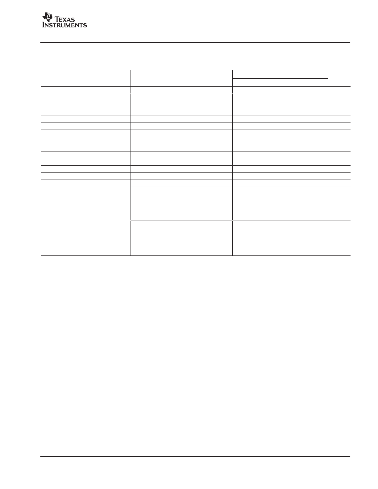
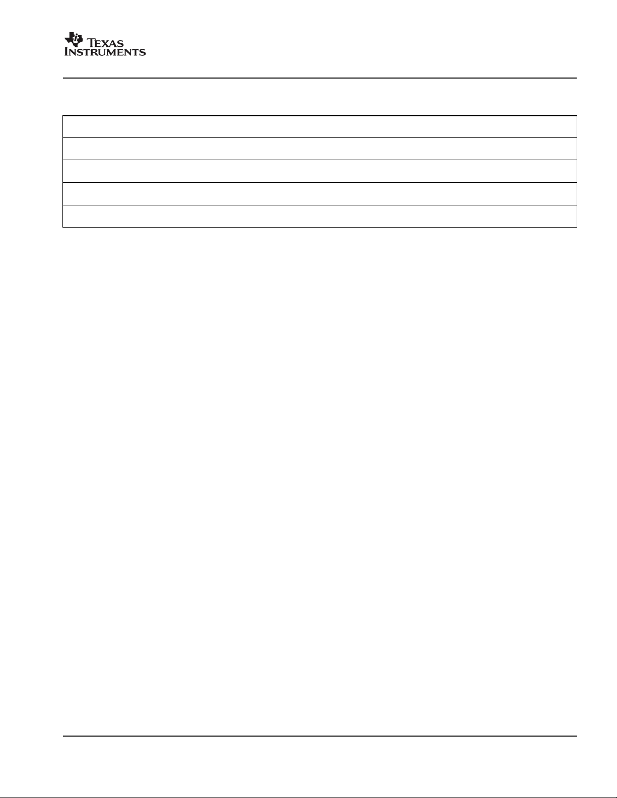
ABSOLUTE MAXIMUM RATINGS
over operat i n g f ree-air temperature range unless otherwise noted
ADS1602 UNIT
AVDD to AGND −0.3 to +6 V
DVDD to DGND −0.3 to +3.6 V
IOVDD to DGND −0.3 to +6 V
AGND to DGND −0.3 to +0.3 V
Input Current 100mA, Momentary
Input Current 10mA, Continuous
Analog I/O to AGND −0.3 to AVDD + 0.3 V
Digital I/O to DGND −0.3 to IOVDD + 0.3 V
Maximum Junction Temperature +150 °C
Operating Temperature Range −40 to +105 °C
Storage Temperature Range −60 to +150 °C
Lead Tem perature (soldering, 10s) +260 °C
(1)
Stresses above these ratings may cause permanent damage.
Exposure to absolute maximum conditions for extended periods
may degrade device reliability. These are stress ratings only , an d
functional operation of the device at these or any other conditions
beyond those specified is not implied.
(1)
This integrated circuit can be damaged by ESD. Texas
Instruments recommends that all integrated circuits be
handled with appropriate precautions. Failure to observe
proper handling and installation procedures can cause damage.
ADS1602 passes standard 200V machine model and 1.5K CDM
testing. ADS1602 passes 1kV human body model testing (TI Standard
is 2kV).
ESD damage can range from subtle performance degradation to
complete device failure. Precision integrated circuits may be more
susceptible t o damage because very small parametric changes could
cause the device not to meet its published specifications.
2
Page 3
"#$%&
Signal-to-noise ratio (SNR)
Total harmonic distortion (THD)
Signal-to-noise + distortion (SINAD)
Spurious-free dynamic range (SFDR)
www.ti.com
SBAS341B − DECEMBER 2004 − REVISED APRIL 2005
ELECTRICAL CHARACTERISTICS
All specifications at TA = −40°C to +85°C, AVDD = 5V, DVDD = IOVDD = 3V, f
and R
Analog Input
Differential input voltage (VIN)
(AINP − AINN)
Common-mode input voltage (VCM)
(AINP + AINN) / 2
Absolute input voltage
(AINP or AINN with respect to AGND)
Dynamic Specifications
Data Rate
Signal-to-noise ratio (SNR)
Total harmonic distortion (THD)
Signal-to-noise + distortion (SINAD)
Spurious-free dynamic range (SFDR)
Intermodulation distortion (IMD)
Aperture delay 4 ns
= 37kΩ, unless otherwise noted.
BIAS
PARAMETER TEST CONDITIONS MIN TYP MAX UNIT
0dBFS ±V
fIN = 10kHz, −1dBFS 92 dB
fIN = 10kHz, −3dBFS 87 90 dB
fIN = 10kHz, −6dBFS 84 87 dB
fIN = 100kHz, −1dBFS 91 dB
fIN = 100kHz, −3dBFS 87 89 dB
fIN = 100kHz, −6dBFS 84 86 dB
fIN = 800kHz, −1dBFS 91 dB
fIN = 800kHz, −3dBFS 89 dB
fIN = 800kHz, −6dBFS 86 dB
fIN = 10kHz, −1dBFS −94 dB
fIN = 10kHz, −3dBFS −106 −92 dB
fIN = 10kHz, −6dBFS −108 −93 dB
fIN = 100kHz, −1dBFS −90 dB
fIN = 100kHz, −3dBFS −96 −90 dB
fIN = 100kHz, −6dBFS −101 −92 dB
fIN = 800kHz, −1dBFS −116 dB
fIN = 800kHz, −3dBFS −114 dB
fIN = 800kHz, −6dBFS −110 dB
fIN = 10kHz, −1dBFS 89 dB
fIN = 10kHz, −3dBFS 85 90 dB
fIN = 10kHz, −6dBFS 82 87 dB
fIN = 100kHz, −1dBFS 87 dB
fIN = 100kHz, −3dBFS 85 88 dB
fIN = 100kHz, −6dBFS 82 86 dB
fIN = 800kHz, −1dBFS 91 dB
fIN = 800kHz, −3dBFS 89 dB
fIN = 800kHz, −6dBFS 86 dB
fIN = 10kHz, −1dBFS 95 dB
fIN = 10kHz, −3dBFS 90 107 dB
fIN = 10kHz, −6dBFS 93 112 dB
fIN = 100kHz, −1dBFS 91 dB
fIN = 100kHz, −3dBFS 90 96 dB
fIN = 100kHz, −6dBFS 93 103 dB
fIN = 800kHz, −1dBFS 120 dB
fIN = 800kHz, −3dBFS 119 dB
fIN = 800kHz, −6dBFS 114 dB
f1 = 995kHz, −6dBFS
f2 = 1005kHz, −6dBFS
= 40MHz, External V
CLK
= +3V , VCM = +1.45V ,
REF
ADS1602
REF
1.45 V
−0.1 4.6 V
f
CLK
ǒ
2.50
Ǔ
40MHz
94 dB
V
MSPS
3
Page 4
"#$%&
www.ti.com
SBAS341B − DECEMBER 2004 − REVISED APRIL 2005
ELECTRICAL CHARACTERISTICS (continued)
All specifications at TA = −40°C to +85°C, AVDD = 5V, DVDD = IOVDD = 3V, f
and R
Digital Filter Characteristics
Passband 0
Passband ripple ±0.001 dB
Passband transition
Stop band
Stop band attenuation 75 dB
Group delay
Settling time Complete settling
Static Specifications
Resolution 16 Bits
No missing codes 16 Bits
Input-referred noise 0.5 0.85 LSB, rms
Integral nonlinearity −1dBFS signal 0.75 LSB
Differential nonlinearity 0.25 LSB
Offset error −0.1 %FSR
Offset error drift −0.1 ppmFSR/°C
Gain error 0.25 %
Gain error drift Excluding reference drift 10 ppm/°C
Common-mode rejection At DC 75 dB
Power-supply rejection At DC 65 dB
Internal Voltage Reference REFEN = low
V
REF
VREFP 3.5 4.0 4.3 V
VREFN 0.5 1.0 1.3 V
VMID 2.3 2.5 2.7 V
V
REF
Startup time 15 ms
External Voltage Reference REFEN = high
V
REF
VREFP 3.5 4 4.25 V
VREFN 0.5 1 1.5 V
VMID 2.3 2.5 2.6 V
= 37kΩ, unless otherwise noted.
BIAS
PARAMETER UNITMAXTYPMINTEST CONDITIONS
−0.1dB attenuation
−3.0dB attentuation
= (VREFP − VREFN) 2.75 3 3.25 V
drift 50 ppm/°C
= (VREFP − VREFN) 2.0 3 3.25 V
= 40MHz, External V
CLK
1.4
ǒ
40MHz
f
CLK
= +3V , VCM = +1.45V ,
REF
ADS1602
f
CLK
ǒ
40MHz
ǒ
40MHz
f
CLK
Ǔ
Ǔ
1.15
1.23
Ǔ
40MHZ
ǒ
40MHZ
ǒ
f
CLK
f
CLK
Ǔ
Ǔ
10.4
20.4
1.1
38.6
ǒ
40MHz
ǒ
40MHz
f
f
CLK
CLK
MHz
Ǔ
MHz
MHz
MHz
Ǔ
µs
µs
4
Page 5
"#$%&
Power dissipation
Power dissipation
www.ti.com
SBAS341B − DECEMBER 2004 − REVISED APRIL 2005
ELECTRICAL CHARACTERISTICS (continued)
All specifications at TA = −40°C to +85°C, AVDD = 5V, DVDD = IOVDD = 3V, f
and R
Clock Input
Frequency (f
Duty Cycle f
Digital Input/Output
V
IH
V
IL
V
OH
V
OL
Input leakage DGND < V
Power-Supply Requirements
AVDD 4.75 5.25 V
DVDD 2.7 3.3 V
IOVDD IOH = 50µA 2.7 5.25 V
AVDD current (I
DVDD current (I
IOVDD current (I
Temperature Range
Specified −40 +85 °C
Operating −40 +105 °C
Storage −60 +150 °C
= 37kΩ, unless otherwise noted.
BIAS
PARAMETER UNITMAXTYPMINTEST CONDITIONS
) 40 MHz
CLK
= 40MHz 45 55 %
CLK
IOH = 50µA IOVDD − 0.5 V
IOL = 50µA DGND + 0.5 V
< IOVDD ±10 µA
DIGIN
)
AVDD
) IOVDD = 3V 25 30 mA
DVDD
) IOVDD = 3V 8 10 mA
IOVDD
REFEN = low 110 125 mA
REFEN = high 88 98 mA
AVDD = 5V, DVDD = 3V,
IOVDD = 3V, REFEN
PD = low, CLK disabled 10 mW
= high
= 40MHz, External V
CLK
0.7 x IOVDD IOVDD V
= +3V , VCM = +1.45V ,
REF
ADS1602
DGND 0.3 x IOVDD V
530 610 mW
5
Page 6

"#$%&
SBAS341B − DECEMBER 2004 − REVISED APRIL 2005
DEFINITIONS
www.ti.com
Absolute Input Voltage
Absolute input voltage, given in volts, is the voltage of each
analog input (AINN or AINP) with respect to AGND.
Aperture Delay
Aperture delay is the delay between the rising edge of CLK
and the sampling of the input signal.
Common-Mode Input Voltage
Common-mode input voltage (VCM) is the average voltage
of the analog inputs:
(AINP ) AINN)
2
Differential Input Voltage
Differential input voltage (VIN) is the voltage difference
between the analog inputs (AINP−AINN).
Differential Nonlinearity (DNL)
DNL, given in least-significant bits of the output code
(LSB), is the maximum deviation of the output code step
sizes from the ideal value of 1LSB.
Full-Scale Range (FSR)
FSR is the difference between the maximum and minimum
measurable input signals (FSR = 2V
REF
).
Gain Error
Gain error, given in %, is the error of the full-scale input
signal with respect to the ideal value.
Gain Error Drift
Gain error drift, given in ppm/_C, is the drift over
temperature of t h e g a i n e r r o r. The gain error is specified as
the larger of the drift from ambient (T = 25_C) to the
minimum or maximum operating temperatures.
Integral Nonlinearity (INL)
INL, given in least-significant bits of the output code (LSB),
is the maximum deviation of the output codes from a best
fit line.
Intermodulation Distortion (IMD)
IMD, given in dB, is measured while applying two input
signals of the same magnitude, but with slightly different
frequencies. It is calculated as the difference between the
rms amplitude of the input signal to the rms amplitude of
the peak spurious signal.
Offset Error
Offset Error , given in % of FSR, is the output reading when
the differential input is zero.
Offset Error Drift
Offset error drift, given in ppm of FSR/_C, is the drift over
temperature of the of fset error. The offset error is specified
as the larger of the drift from ambient (T = 25_C) to the
minimum or maximum operating temperatures.
Signal-to-Noise Ratio (SNR)
SNR, given in dB, is the ratio of the rms value of the input
signal to the sum of all the frequency components below
f
/2 (the Nyquist frequency) excluding the first six
CLK
harmonics of the input signal and the dc component.
Signal-to-Noise and Distortion (SINAD)
SINAD, given in dB, is the ratio of the rms value of the input
signal to the sum of all the frequency components below
f
/2 (the Nyquist frequency) including the harmonics of
CLK
the input signal but excluding the dc component.
Spurious-Free Dynamic Range (SFDR)
SFDR, given in dB, is the difference between the rms
amplitude of the input signal to the rms amplitude of the
peak spurious signal.
Total Harmonic Distortion (THD)
THD, given in dB, is the ratio of the sum of the rms value
of the first six harmonics of the input signal to the rms value
of the input signal.
6
Page 7
www.ti.com
FUNCTION
DESCRIPTION
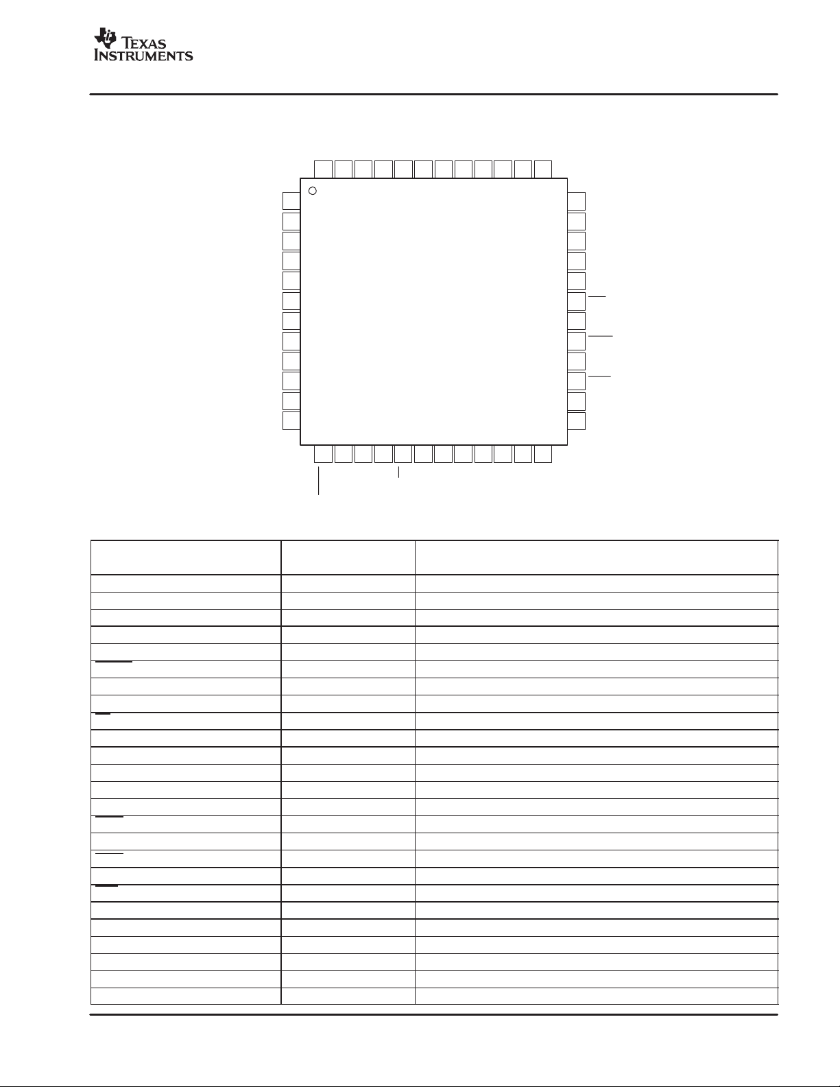
PIN ASSIGNMENTS
VREFP
VREFP
VMID
VREFN
VREFN
VCAP
AVDD
AGND
CLK
AGND
48 47 46 45 44 43 42 41 40 39 38
"#$%&
SBAS341B − DECEMBER 2004 − REVISED APRIL 2005
DGND
IOVDD
NC
36
DGND
35
NC
34
DVDD
33
DGND
32
FSO
31
FSO
30
DOUT
29
DOUT
28
SCLK
27
SCLK
26
NC
25
NC
TQFP PACKAGE
(TOP VIEW)
AGND
AVDD
AGND
AINN
AINP
AGND
AVDD
RBIAS
AGND
AVDD
AGND
AVDD
1
2
3
4
5
6
7
8
9
10
11
12
13 14 15 16 17 18 19 20 21 22 233724
NC
REFEN
RPULLUP
NC
ADS1602
PD
DVDD
SYNC
DGND
OTR
DVDD
DGND
Terminal Functions
TERMINAL
NAME NO.
AGND 1, 3, 6, 9, 11, 39, 41 Analog Analog ground
AVDD 2, 7, 10, 12, 42 Analog Analog supply
AINN 4 Analog input Negative analog input
AINP 5 Analog input Positive analog input
RBIAS 8 Analog Terminal for external analog bias setting resistor.
REFEN 13 Digital input: active low Internal reference enable. Internal pull-down resistor of 170kΩ to DGND.
NC 14, 16, 24−26, 35 Do not connect These terminals must be left unconnected.
RPULLUP 15 Digital Input Pull-up to DVDD with 10kΩ resistor (see Figure 53).
PD 17 Digital input: active low Power down all circuitry. Internal pull-up resistor of 170kΩ to DGND.
DVDD 18, 23, 34 Digital Digital supply
DGND 19, 22, 33, 36, 38 Digital Digital ground
SYNC 20 Digital input Synchronization control input
OTR 21 Digital output Indicates analog input signal is out of range.
SCLK 28 Digital output Serial clock output
SCLK 27 Digital output Serial clock output, complementary signal.
DOUT 30 Digital output Data output
DOUT 29 Digital output Data output, complementary signal.
FSO 32 Digital output Frame synchronization output
FSO 31 Digital output Frame synchronization output, complementary signal.
IOVDD 37 Digital Digital I/O supply
CLK 40 Digital input Clock input
VCAP 43 Analog Terminal for external bypass capacitor connection to internal bias voltage.
VREFN 44, 45 Analog Negative reference voltage
VMID 46 Analog Midpoint voltage
VREFP 47, 48 Analog Positive reference voltage
7
Page 8

"#$%&
t
Settling time of ADS1602
(1)
www.ti.com
SBAS341B − DECEMBER 2004 − REVISED APRIL 2005
TIMING DIAGRAMS
CLK
t
STL
SYNC
FSO
TIMING REQUIREMENTS
For TA = −40°C to +85°C, DVDD = 2.7V to 3.6V, IOVDD = 2.7V to 5.25V.
SYMBOL DESCRIPTION MIN TYP MAX UNIT
t
SYPW
STL
NOTE:(1) An FSO pulse occuring prior to T
SYNC positive pulse width
t
SYPW
Figure 1. Initialization Timing
≥ 816 CLK period should be ignored.
STL
2 16 CLK periods
51 52 Conversions
816 832 CLK periods
t
DPD
t
CPW
t
CPW
Bit 1 Bit 0 (LSB)Bit 15 (MSB) Bit14
New Data
CLK
FSO
SCLK
DOUT
t
C
t
CF
t
FPW
t
CS
t
DHD
Bit 0 (LSB)
Old Data
Figure 2. Data Retrieval Timing
TIMING REQUIREMENTS
For TA = −40°C to +85°C, DVDD = 2.7V to 3.6V, IOVDD = 2.7V to 5.25V.
SYMBOL DESCRIPTION MIN TYP MAX UNIT
t
C
t
CPW
t
CF
t
FPW
t
CS
t
DHD
t
DPD
CLK period (1/f
CLK
)
CLK positive or negative pulse width
Rising edge of CLK to rising edge of FSO
FSO positive pulse width
Rising edge of CLK to rising edge of SCLK
SCLK rising edge to old DOUT invalid (hold time)
SCLK rising edge to new DOUT valid (propagation delay)
25 ns
11.25 ns
15 ns
1 CLK period
15 ns
0 ns
5 ns
8
Page 9

www.ti.com
SPECTRAL RESPONSE
SPECTRAL RESPONSE
SPECTRAL RESPONSE
SPECTRAL RESPONSE
SPECTRAL RESPONSE
SPECTRAL RESPONSE
TYPICAL CHARACTERISTICS
All specifications at TA = 25°C, AVDD = 5V, DVDD = IOVDD = 3V, f
unless otherwise noted.
= 40MHz, External V
CLK
"#$%&
SBAS341B − DECEMBER 2004 − REVISED APRIL 2005
= +3V , VCM = +1.45V , and R
REF
BIAS
= 37kΩ,
0
−
20
−
40
−
60
−
80
−
100
Amplitude (dB)
−
120
−
140
−
160
0 200 400 600
0
−
20
−
40
−
60
−
80
−
100
Amplitude (dB)
−
120
−
140
−
160
0 200 400 600
Frequency (kHz)
Figure 3
Frequency (kHz)
fIN= 10kHz,−1dBFS
SNR = 92dB
THD =−94dB
SFDR = 95dB
800 1000 1200
fIN= 10kHz,−10dBFS
SNR = 83dB
THD =−105dB
SFDR = 110dB
800 1000 1200
0
−
20
−
40
−
60
−
80
−
100
Amplitude (dB)
−
120
−
140
−
160
0 200 400 600
Figure 4
0
−
20
−
40
−
60
−
80
−
100
Amplitude (dB)
−
120
−
140
−
160
0200400600
fIN= 10kHz,−6dBFS
SNR= 87dB
THD =−108dB
SFDR = 112dB
800 1000 1200
Frequency(kHz)
fIN= 100kHz,−1dBFS
SNR = 90dB
THD =−90dB
SFDR = 91dB
800 1000 1200
Frequency (kHz)
0
−
20
−
40
−
60
−
80
−
100
Amplitude (dB)
−
120
−
140
−
160
0 200 400 600
Figure 5
Frequency (kHz)
Figure 7
fIN= 100kHz,−6dBFS
SNR = 86dB
THD =−101dB
SFDR = 103dB
800 1000 1200
0
−
20
−
40
−
60
−
80
−
100
Amplitude (dB)
−
120
−
140
−
160
0 200 400 600
Figure 6
fIN=100kHz,−10dBFS
SNR = 82dB
THD =−100dB
SFDR = 102dB
800 1000 1200
Frequency (kHz)
Figure 8
9
Page 10

"#$%&
SPECTRAL RESPONSE
SPECTRAL RESPONSE
SPECTRAL RESPONSE
SPECTRAL RESPONSE
SPECTRAL RESPONSE
Figure 14
SPECTRAL RESPONSE
SBAS341B − DECEMBER 2004 − REVISED APRIL 2005
TYPICAL CHARACTERISTICS (continued)
All specifications at TA = 25°C, AVDD = 5V, DVDD = IOVDD = 3V, f
unless otherwise noted.
= 40MHz, External V
CLK
= +3V , VCM = +1.45V , and R
REF
www.ti.com
= 37kΩ,
BIAS
0
−
20
−
40
−
60
−
80
−
100
Amplitude (dB)
−
120
−
140
−
160
0
200 400 600
Frequency (kHz)
fIN= 504kHz,−1dBFS
SNR= 91dB
THD =−119dB
SFDR = 119dB
800 1000 1200
Figure 9
0
−
20
−
40
−
60
−
80
−
100
Amplitude (dB)
−
120
−
140
−
160
0
200 400 600
Frequency (kHz)
fIN=504kHz,−10dBFS
SNR = 82dB
THD =−96dB
SFDR = 96dB
800 1000 1200
0
−
20
−
40
−
60
−
80
−
100
Amplitude (dB)
−
120
−
140
−
160
0
200 400 600
Frequency (kHz)
fIN= 504kHz,−6dBFS
SNR = 86dB
THD =−103dB
SFDR = 103dB
800 1000 1200
Figure 10
0
fIN= 799kHz,−1dBFS
−
20
SNR = 91dB
THD =−116dB
−
40
SFDR= 120dB
−
60
−
80
−
100
Amplitude (dB)
−
120
−
140
−
160
0
200 400 600
Frequency (kHz)
800 1000 1200
10
Figure 11
0
fIN= 799kHz,−6dBFS
−
20
SNR = 86dB
THD =−110dB
−
40
SFDR = 114dB
−
60
−
80
−
100
Amplitude (dB)
−
120
−
140
−
160
0
200 400 600
Frequency (kHz)
800 1000 1200
0
fIN= 799kHz,−10dBFS
−
20
SNR = 82dB
THD =−107dB
−
40
SFDR = 112dB
−
60
−
80
−
100
Amplitude (dB)
−
120
−
140
−
160
0
Figure 12
200 400 600
Frequency (kHz)
800 1000 1200
Figure 13
Page 11

www.ti.com
SNR, THD, and SFDR vs INPUT SIGNAL AMPLITUDE
SNR, THD, and SFDR vs INPUT SIGNAL AMPLITUDE
SNR, THD, and SFDR vs INPUT SIGNAL AMPLITUDE
SNR, THD, and SFDR vs INPUT SIGNAL AMPLITUDE
SIGNAL−TO− NOISE RATIO
TYPICAL CHARACTERISTICS (continued)
All specifications at TA = 25°C, AVDD = 5V, DVDD = IOVDD = 3V, f
unless otherwise noted.
= 40MHz, External V
CLK
"#$%&
SBAS341B − DECEMBER 2004 − REVISED APRIL 2005
= +3V , VCM = +1.45V , and R
REF
BIAS
= 37kΩ,
140
120
100
80
60
SIGNAL−TO−NOISE RATIO,
40
TOTALHARMONIC DISTORTION,
20
SPURIOUS−FREE DYNAMIC RANGE (dB)
−80−70−60−50−40−30−20−
Input Signal Amplitude, V
SFDR
THD
IN
SNR
fIN=10kHz
10 0
(dB)
Figure 15
140
120
100
80
60
SIGNAL−TO−NOISE RATIO,
40
TOTAL HARMONICDISTORTION,
20
SPURIOUS−FREE DYNAMIC RANGE (dB)
−
80−70−60−50−40−30−20−10 0
SFDR
THD
Input Signal Amplitude, V
(dB)
IN
SNR
fIN= 100kHz
120
110
100
90
80
70
60
50
40
SIGNAL−TO−NOISE RATIO,
TOTALHARMONIC DISTORTION,
30
20
SPURIOUS−FREE DYNAMIC RANGE (dB)
−80−70−60−50−40−30−20−
Input Signal Amplitude, V
SFDR
THD
IN
SNR
fIN=50kHz
10 0
(dB)
Figure 16
140
120
100
80
60
SIGNAL−TO−NOISE RATIO,
40
TOTAL HARMONICDISTORTION,
20
SPURIOUS−FREE DYNAMIC RANGE (dB)
−80−70−60−50−40−30−20−
Input Signal Amplitude, V
SFDR
SNR
THD
IN
fIN= 500kHz
10 0
(dB)
Figure 17
SNR, THD, and SFDR vs INPUT SIGNALAMPLITUDE
140
120
100
80
60
SIGNAL−TO−NOISE RATIO,
40
TOTALHARMONIC DISTORTION,
20
SPURIOUS−FREE DYNAMIC RANGE (dB)
−
80−70−60−50−40−30−20−10 0
Input Signal Amplitude, V
SFDR
SNR
Figure 19
THD
IN
(dB)
fIN= 800kHz
Figure 18
95
90
85
SNR (dB)
80
75
70
10k100k1M
vs INPUT FREQUENCY
Input Frequency, f
(Hz)
IN
VIN=−1dB
V
IN
V
=−10dB
IN
=−6dB
Figure 20
11
Page 12

"#$%&
TOTAL HARMONIC DISTORTION
SPURIOUS−FREE DYNAMIC RANGE
SIGNAL−TO−NOISERATIO
TOTAL HARMONICDISTORTION
SPURIOUS−FREE DYNAMICRANGE
SBAS341B − DECEMBER 2004 − REVISED APRIL 2005
TYPICAL CHARACTERISTICS (continued)
All specifications at TA = 25°C, AVDD = 5V, DVDD = IOVDD = 3V, f
unless otherwise noted.
= 40MHz, External V
CLK
= +3V , VCM = +1.45V , and R
REF
www.ti.com
= 37kΩ,
BIAS
−
80
−
85
−
90
−
95
−
100
THD (dB)
−
105
−
110
−
115
−
120
10k 100k 1M
vs INPUT FREQUENCY
VIN=−1dB
Input Frequency, f
(Hz)
IN
VIN=−10dB
V
IN
=−6dB
Figure 21
93
92
91
90
89
SNR (dB)
88
87
86
85
1.01.41.82.22.63.03.4
vs INPUT COMMON−MODE VOLTAGE
fIN=10kHz,VIN=−1dB
fIN= 100kHz,VIN=−6dB
Input Common−Mode Voltage, VCM(V)
fIN= 100kHz,VIN=−1dB
fIN=10kHz,VIN=−6dB
Figure 23
130
120
110
VIN=−6dB
100
SFDR (dB)
90
80
70
10k 100k 1M
vs INPUT FREQUENCY
VIN=−10dB
VIN=−1dB
Input Frequency, fIN(Hz)
Figure 22
−
70
−
80
−
90
THD (dB)
−
100
−
110
1.0 1.4 1.8 2.2 2.6 3.0 3.4
vs INPUT COMMON−MODE VOLTAGE
fIN=100kHz,VIN=−1dB
fIN=10kHz,VIN=−1dB
fIN=100kHz,VIN=−6dB
fIN= 10kHz, VIN=−6dB
Input Common−Mode Voltage, VCM(V)
Figure 24
12
110
105
100
95
SFDR(dB)
90
85
80
1.0 1.4 1.8 2.2 2.6 3.0 3.4
vs INPUT COMMON−MODE VOLTAGE
fIN= 10kHz, VIN=−6dB
fIN= 100kHz,VIN=−6dB
fIN=10kHz
=−1dB
V
IN
fIN= 100kHz, VIN=−1dB
Input Common−Mode Voltage, VCM(V)
Figure 25
3
2
1
0
Offset (LSB)
−
1
−
2
−
3
0 100 200 300 400 500 600 700 800 900 1000
OFFSET DRIFT OVER TIME
TimeInterval (s)
Figure 26
Page 13

www.ti.com
SIGNAL−TO−NOISERATIO
TOTAL HARMONICDISTORTION
SPURIOUS−FREE DYNAMIC RANGE
POWER−SUPPLY CURRENT
TYPICAL CHARACTERISTICS (continued)
All specifications at TA = 25°C, AVDD = 5V, DVDD = IOVDD = 3V, f
unless otherwise noted.
= 40MHz, External V
CLK
"#$%&
SBAS341B − DECEMBER 2004 − REVISED APRIL 2005
= +3V , VCM = +1.45V , and R
REF
BIAS
= 37kΩ,
100
vs CLOCK FREQUENCY
VIN=−6dBFS, fIN=10kHz
90
R
BIAS
= 30k
Ω
R
BIAS
80
70
= 210k
Ω
R
60
SNR (dB)
BIAS
R
BIAS
=140k
R
BIAS
Ω
= 100k
Ω
50
=267k
Ω
R
40
BIAS
30
5 101520253035404550
Clock Frequency, f
CLK
(MHz)
Figure 27
110
100
90
80
R
70
60
SFDR (dB)
50
40
30
20
BIAS
R
BIAS
R
VIN=−6dBFS, fIN= 10kHz
5 101520253035404550
vs CLOCK FREQUENCY
Ω
=267k
Ω
=210k
Ω
= 140k
BIAS
Clock Frequency, f
= 37k
CLK
Ω
R
BIAS
=60k
(MHz)
Ω
R
BIAS
=100k
R
BIAS
Figure 29
R
= 30k
Ω
= 37k
R
BIAS
= 60k
BIAS
110
Ω
100
R
BIAS
90
80
R
Ω
70
60
THD (dB)
BIAS
R
50
40
30
VIN=−6dBFS, fIN= 10kHz
20
5 101520253035404550
BIAS
R
= 267k
=210k
BIAS
Ω
Ω
= 140k
Ω
Clock Frequency, f
=37k
CLK
Ω
R
BIAS
= 60k
(MHz)
Ω
R
BIAS
= 100k
R
BIAS
=30k
Ω
Ω
Figure 28
vs CLOCK FREQUENCY
NOISE vs DC INPUT VOLTAGE
1000
100
Ω
10
RMS Noise (LSB)
1
0.1
−
−
3
−
2
13012
Input DC Voltage (V)
Figure 30
1540
NOISE HISTOGRAM
1400
1300
1200
1100
1000
900
800
700
600
Occurrences
500
400
300
200
100
0
−
4−3−2−101 2 34
Output Code (LSB)
Figure 31
VIN=0
120
100
Current (mA)
vs TEMPERATURE
I
(REFEN= low)
AVDD
I
(REFEN = high)
80
AVDD
60
40
I
20
R
=37kΩ,f
BIAS
0
−
40
−
=40MHz
CLK
15 10 35 60 85
DVDD+IIOVDD
Temperature(_C)
Figure 32
13
Page 14

"#$%&
SUPPLY−CURRENT vs CLOCK FREQUENCY
ANALOG SUPPLY CURRENTvs R
SIGNAL−TO−NOISE RATIO vs TEMPERATURE
TOTALHARMONIC DISTORTION vs TEMPERATURE
SPURIOUS−FREE DYNAMIC RANGE
SBAS341B − DECEMBER 2004 − REVISED APRIL 2005
TYPICAL CHARACTERISTICS (continued)
All specifications at TA = 25°C, AVDD = 5V, DVDD = IOVDD = 3V, f
unless otherwise noted.
= 40MHz, External V
CLK
= +3V , VCM = +1.45V , and R
REF
www.ti.com
= 37kΩ,
BIAS
140
120
100
80
60
40
Supply Current (mA)
20
0
0 5 10 15 20 25 30 35 40
VIN=−6dBFS, fIN=10kHz, R
I
(REFEN = low)
AVDD
I
(REFEN = high)
AVDD
I
IOVDD+IDVDD
Clock Frequency,f
CLK
(MHz)
Figure 33
100
95
90
85
SNR (dB)
80
=37k
BIAS
VIN=−1dB
VIN=−6dB
VIN=−10dB
CLK
(REFEN = l ow)
AVDD
(REFEN = high)
BIAS
=40MHz
Ω
130
110
(mA)
AVDD
90
70
50
30
Analog Supply Current, I
10
0 50 100 150 200 250 300
VIN=−6dBFS, fIN=10kHz,f
I
I
AVDD
R
(kΩ)
BIAS
Figure 34
−
80
−
85
VIN=−1dB
−
90
V
=−6dB
THD (dB)
IN
−
95
75
fIN= 100kHz
70
−
40
−
15 10 35 60 85
Temperature (_C)
Figure 35
120
115
110
105
100
SFDR (dB)
95
90
VIN=−1dB
85
80
−
40
VIN=−10dB
V
IN
−
VIN=−10dB
−
100
−
105
−
40
vs TEMPERATURE
=−6dB
15 10 35 60 85
Temperature (_C)
−
15 10 35 60 85
Figure 37
Temperature (_C)
Figure 36
14
Page 15

www.ti.com
"#$%&
SBAS341B − DECEMBER 2004 − REVISED APRIL 2005
OVERVIEW
The ADS1602 is a high-performance delta-sigma ADC.
The modulator uses an inherently stable 2-1-1 multi-stage
architecture incorporating proprietary circuitry that allows
for very linear high-speed operation. The modulator
samples the input signal at 40MSPS (when f
A low-ripple linear phase digital filter decimates the
modulator output by 16 to provide high resolution 16-bit
output data.
Conceptually, the modulator and digital filter measure the
differential input signal, V
scaled differential reference, V
= (AINP – AINN), against the
IN
= (VREFP – VREFN),
REF
as shown in Figure 38. The voltage reference can either be
generated internally or supplied externally . A 3-wire serial
interface, designed for direct connection to DSPs, outputs
the data. A separate power supply for the I/O allows flexibility for interfacing to different logic families. Out-of-range
conditions are indicated with a dedicated digital output pin.
Analog power dissipation is controlled using an external
resistor. This control allows reduced dissipation when operating at slower speeds. When not in use, power consumption can be dramatically reduced by setting the PD
pin low to enter Power-Down mode.
ANALOG INPUTS (AINP, AINN)
The ADS1602 measures the differential signal,
V
= (AINP – AINN), against the differential reference,
IN
V
= (VREFP – VREFN). The most positive measurable
REF
differential input is V
, which produces the most positive
REF
= 40MHz).
CLK
digital output code of 7FFFh. Likewise, the most negative
measurable dif ferential input is –V
, which produces the
REF
most negative digital output code of 8000h.
The ADS1602 supports a very wide range of input signals.
For V
= 3V, the full-scale input voltages are ±3V.
REF
Having such a wide input range makes out-of-range
signals unlikely. However, should an out-of-range signal
occur, the digital output OTR will go high.
The analog inputs must be driven with a differential signal
to achieve optimum performance. For the input signal:
V
AINP) AINN
+
CM
2
the recommended common-mode voltage is 1.5V. In
addition to the differential and common-mode input
voltages, the absolute input voltage is also important. This
is the voltage on either input (AINP or AINN) with respect
to AGND. The range for this voltage is:
* 0.1V t (AINN or AIN P) t 4.6V
If either input is taken below –0.1V, ESD protection diodes
on the inputs will turn on. Exceeding 4.6V on either input
will result in degradation in the linearity performance. ESD
protection diodes will also turn on if the inputs are taken
above AVDD (+5V).
The recommended absolute input voltage is:
* 0.1V t (AINN or AIN P) t 4.2V
Keeping the inputs within this range provides for optimum
performance.
AINP
AINN
VREFN IOVDDVREFP
Σ
V
REF
V
IN
Σ
Σ∆
Modulator
Digital
Filter
Serial
Interface
Figure 38. Conceptual Block Diagram
CLK
FSO
FSO
SCLK
SCLK
DOUT
DOUT
15
Page 16

"#$%&
SBAS341B − DECEMBER 2004 − REVISED APRIL 2005
www.ti.com
INPUT CIRCUITRY
The ADS1602 uses switched-capacitor circuitry to measure
the input voltage. Internal capacitors are charged by the
inputs and then discharged internally with this cycle
repeating at the frequency of CLK. Figure 39 shows a
conceptual diagram of these circuits. Switches S2 represent
the net effect of the modulator circuitry in discharging the
sampling capacitors; the actual implementation is different.
The timing for switches S1 and S2 is shown in Figure 40.
ADS1602
8pF
VMID
8pF
VMID
S
2
S
2
AINP
AINN
AGND
S
1
10pF
S
1
10pF
Figure 39. Conceptual Diagram of Internal
Circuitry Connected to the Analog Inputs
t
=1/f
S1
S2
SAMPLE
On
Off
On
Off
CLK
external capacitors, between the inputs and from each
input to AGND, improve linearity and should be placed as
close to the pins as possible. Place the drivers close to the
inputs and use good capacitor bypass techniques on their
supplies, such as a smaller high-quality ceramic capacitor
in parallel with a larger capacitor. Keep the resistances
used in the driver circuits low—thermal noise in the driver
circuits degrades the overall noise performance. When the
signal can be ac-coupled to the ADS1602 inputs, a simple
RC filter can set the input common-mode voltage. The
ADS1602 is a high-speed, high-performance ADC.
Special care must be taken when selecting the test
equipment and setup used with this device. Pay particular
attention to the signal sources to ensure they do not limit
performance when measuring the ADS1602.
Ω
392
Ω
392
V
IN
−
2
Ω
392
(1)
V
CM
Ω
Ω
392
V
IN
2
Ω
392
(1)
V
CM
Ω
(1) Recommended VCM=1.5V.
(2) Optional ac−coupling circuit provides common−mode input voltage.
(3) Increaseto 390pF when f
40pF
OPA2822
1µF392
392
40pF
OPA2822
1µF392
0.01µF
(2)
Ω
1k
Ω
100kHz for improvedSNRandTHD.
≤
IN
(1)
V
CM
1k
0.01µF
(2)
(2)
Ω
(2)
49.9
100pF
100pF
49.9
100pF
Ω
Ω
AGND
AINP
(3)
ADS1602
AINN
Figure 41. Recommended Driver Circuit Using the
OPA2822
Figure 40. Timing for the Switches in Figure 39
DRIVING THE INPUTS
The external ci rcuits driving the ADS1602 inputs must be
able to h andle t he l oad p resented b y the switching c apacitors
within the ADS1602. The input switches S1 in Figure 39 are
closed for approximately one-half of the sampling period,
t
, allowing only ≈ 11ns for the internal capacitors to be
sample
charged by the inputs when f
= 40MHz.
CLK
Figure 41 and Figure 42 show the recommended circuits
when using single-ended or differential op amps,
respectively. The analog inputs must be driven
differentially to achieve optimum performance. The
16
22pF
+V
−V
24.9Ω
Ω
392Ω
IN
IN
392
V
CM
Ω
392
THS4503
392
22pF
Ω
24.9
100pF
100pF
Ω
100pF
AINP
ADS1602
AINN
Figure 42. Recommended Driver Circuit Using the
THS4503 Differential Amplifier
Page 17

www.ti.com
"#$%&
SBAS341B − DECEMBER 2004 − REVISED APRIL 2005
REFERENCE INPUTS (VREFN, VREFP, VMID)
The ADS1602 can operate from an internal or external
voltage reference. In either case, the reference voltage
V
is set by the differential voltage between VREFN a nd
REF
VREFP: V
= (VREFP – VREFN). VREFP and VREFN
REF
each use two pins, which should be shorted together.
VMID equals approximately 2.5V and is used by the
modulator. VCAP connects to an internal node and must
also be bypassed with an external capacitor.
INTERNAL REFERENCE (REFEN = LOW)
To use the internal reference, set the REFEN pin low. This
activates the internal circuitry that generates the reference
voltages. The internal reference voltages are applied to
the pins. Good bypassing of the reference pins is critical
to achieve optimum performance and is done by placing
the bypass capacitors as close to the pins as possible.
Figure 43 shows the recommended bypass capacitor
values. Use high-quality ceramic capacitors for the smaller
values. Avoid loading the internal reference with external
circuitry. I f the ADS1602 internal reference is to be used by
other circuitry, buffer the reference voltages to prevent
directly loading the reference pins.
ADS1602
VREFP
10µF
0.1µF
10µF 0.1µF
10µF 0.1µF
0.1µF
AGND
VREFP
VMID
VREFN
VREFN
VCAP
0.1µF
Figure 43. Reference Bypassing When Using the
Internal Reference
of providing both a dc and a transient current. Figure 44
shows a simplified diagram of the internal circuitry of the
reference when the internal reference is disabled. As with
the input circuitry, switches S1 and S2 open and close as
shown by the timing in Figure 40.
ADS1602
S
VREFP
VREFP
VREFN
VREFN
1
S
Ω
S
1
50pF300
2
Figure 44. Conceptual Internal Circuitry for the
Reference When REFEN = High
Figure 45 shows the recommended circuitry for driving
these reference inputs. Keep the resistances used in the
buffer circuits low to prevent excessive thermal noise from
degrading performance. Layout of these circuits is critical;
be sure to follow good high-speed layout practices. Place
the buffers, and especially the bypass capacitors, as close
to the pins as possible. VCAP is unaffected by the setting
on REFEN
and must be bypassed when using the internal
or an external reference.
392Ω
0.001µF
ADS1602
VREFP
VREFP
0.1µF
VMID
0.1µF
VREFN
VREFN
2.5V
OPA2822
4V
Ω
392
0.001µF
OPA2822
392Ω
0.001µF
OPA2822
1V
10µF
0.1µF
10µF
10µF 0.1µF
EXTERNAL REFERENCE (REFEN = HIGH)
To use an external reference, set the REFEN pin high. This
deactivates the internal generators for VREFP, VREFN
and VMID, and saves approximately 25mA of current on
the analog supply (AVDD). The voltages applied to these
pins must be within the values specified in the Electrical
Characteristics table. Typically, VREFP = 4V, VMID = 2.5V
and VREFN = 1V. The external circuitry must be capable
VCAP
0.1µF
AGND
Figure 45. Recommended Buffer Circuit When
Using an External Reference
17
Page 18

"#$%&
ALLOWABLE
SBAS341B − DECEMBER 2004 − REVISED APRIL 2005
www.ti.com
CLOCK INPUT (CLK)
The ADS1602 requires an external clock signal to be
applied to the CLK input pin. The sampling of the
modulator is controlled by this clock signal. As with any
high-speed data converter, a high quality clock is essential
for optimum performance. Crystal clock oscillators are the
recommended CLK source; other sources, such as
frequency synthesizers, are usually inadequate. Make
sure to avoid excess ringing on the CLK input; keeping the
trace as short as possible will help.
Measuring high-frequency, large amplitude signals
requires tight control of clock jitter. The uncertainty during
sampling of the input from clock jitter limits the maximum
achievable SNR. This effect becomes more pronounced
with higher frequency and larger magnitude inputs.
Fortunately, the ADS1602 oversampling topology reduces
clock jitter sensitivity over that of Nyquist rate converters
such as pipeline and successive approximation
converters by a factor of
Ǹ
16
.
In order to not limit the ADS1602 SNR performance, keep
the jitter on the clock source below the values shown in
Table 1. When measuring lower frequency and lower
amplitude inputs, more CLK jitter can be tolerated. In
determining the allowable clock source jitter, select the
worst-case input (highest frequency, largest amplitude)
that will be seen in the application.
Table 1. Maximum Allowable Clock Source Jitter
for Different Input Signal Frequencies and
Amplitude
INPUT SIGNAL
MAXIMUM
FREQUENCY
1MHz −2dB 3.8ps
1MHz −20dB 28ps
500kHz −2dB 7.6ps
500kHz −20dB 57ps
100kHz −2dB 38ps
100kHz −20dB 285ps
MAXIMUM
AMPLITUDE
MAXIMUM
CLOCK SOURCE
JITTER
DATA FORMAT
The 16-bit output data is in binary two’s complement
format as shown in Table 2. When the input is positive
out-of-range, exceeding the positive full-scale value of
V
, the output clips to all 7FFFh and the OTR output
REF
goes high.
Likewise, when the input is negative out-of-range by going
below the negative full-scale value of –V
, the output
REF
clips to 8000h and the OTR output goes high. The OTR
remains high while the input signal is out-of-range.
Table 2. Output Code Versus Input Signal
INPUT SIGNAL
(INP – INN)
≥ +V
−V
v −V
(1)
Excludes effects of noise, INL, offset and gain errors.
(> 0dB) 7FFFh 1
REF
V
(0dB) 7FFFh 0
REF
+V
REF
215* 1
0 0000h 0
−V
REF
215* 1
15
2
REF
ǒ
REF
215* 1
15
2
ǒ
215* 1
Ǔ
Ǔ
IDEAL OUTPUT
(1)
CODE
0001h 0
FFFFh 0
8000h 0
8000h 1
OTR
OUT-OF-RANGE INDICATION (OTR)
If the output code exceeds the positive or negative
full-scale, the out-of-range digital output OTR will go high
on the falling edge of SCLK. When the output code returns
within the full-scale range, OTR returns low on the falling
edge of SCLK.
DATA RETRIEVAL
Data retrieval is controlled through a simple serial
interface. The interface operates in a master fashion by
outputting both a frame sync indicator (FSO) and a serial
clock (SCLK). Complementary outputs are provided for
the frame sync output (FSO
output (DOUT
). When not needed, leave the
), serial clock (SCLK) and data
complementary outputs unconnected.
18
Page 19

www.ti.com
"#$%&
SBAS341B − DECEMBER 2004 − REVISED APRIL 2005
INITIALIZING THE ADS1602
After the power supplies have stabilized, you must
initialize the ADS1602 by issuing a SYNC pulse as shown
in Figure 1. This operation needs only to be done once
after power-up and does not need to be performed when
exiting the Power-Down mode.
SYNCHRONIZING MULTIPLE ADS1602s
The SYNC input can be used to synchronize multiple
ADS1602s to provide simultaneous sampling. All devices
to be synchronized must use a common CLK input. With
the CLK inputs running, pulse SYNC on the falling edge of
CLK, as shown in Figure 46. Afterwards, the converters
will be converting synchronously with the FSO outputs
updating simultaneously. After synchronization, FSO is
held low until the digital filter has fully settled.
SYNC
CLK
ADS1602
SYNC
CLK
ADS1602
SYNC
CLK
1
FSO
DOUT
2
FSO
DOUT
FSO
DOUT
FSO
DOUT
1
1
2
2
STEP RESPONSE
Figure 47 plots the normalized step response for an input
applied at t = 0. The x-axis units of time are conversions
cycles. It takes 51 cycles to fully settle; for f
= 40MHz,
CLK
this corresponds to 20.4µs.
1.2
1.0
0.8
0.6
0.4
Step Response
0.2
0
−
0.2
010203040
Time(ConversionCycles)
50
Figure 47. Step Response
CLK ...
SYNC
FSO
1
FSO
2
...
t
STL
Figure 46. Synchronizing Multiple Converters
19
Page 20
"#$%&
SBAS341B − DECEMBER 2004 − REVISED APRIL 2005
www.ti.com
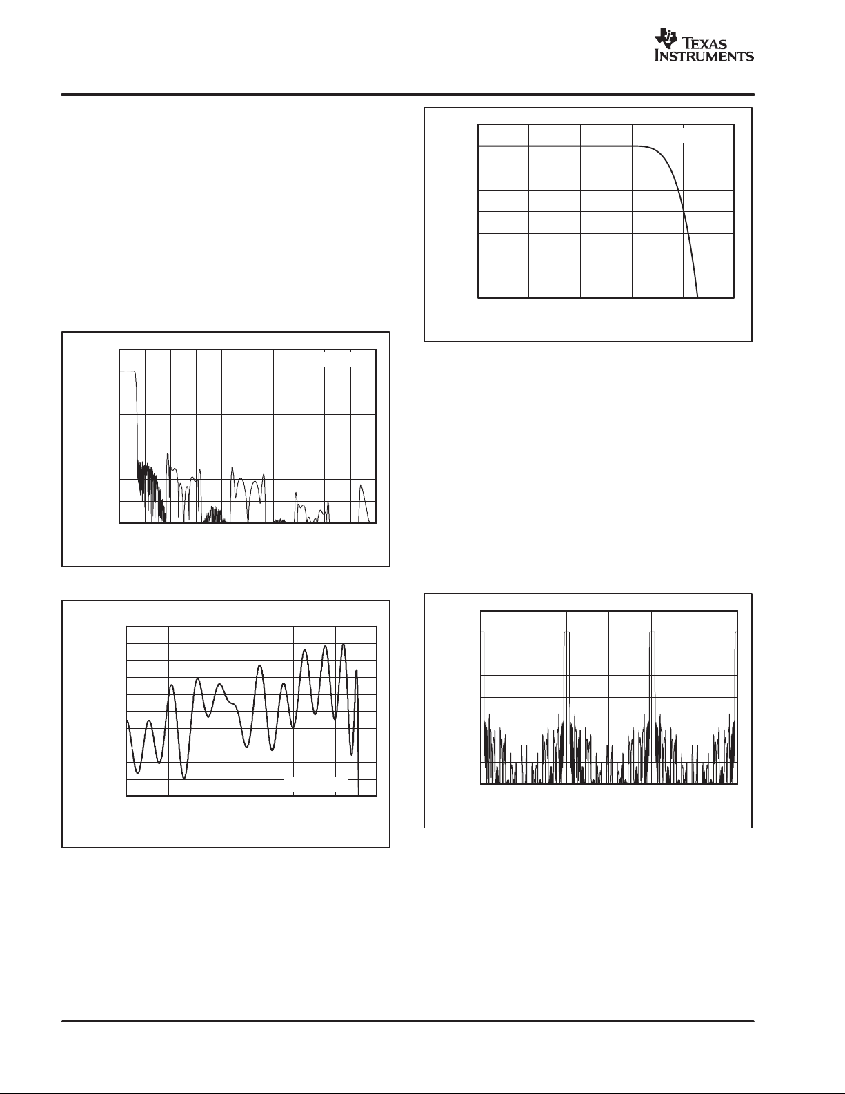
FREQUENCY RESPONSE
The linear phase FIR digital filter sets the overall frequency
response. Figure 48 shows the frequency response from
dc to 20MHz for f
= 40MHz. The frequency response
CLK
of the ADS1602 filter scales directly with CLK frequency.
For example, if the CLK frequency is decreased by half (to
20MHz), the values on the X-axis in Figure 48 would need
to be scaled by half, with the span becoming dc to 10MHz.
Figure 49 shows the passband ripple from dc to 1200kHz
(f
= 40MHz). Figure 50 shows a closer view of the
CLK
passband transition by plotting the response from 900kHz
to 1300kHz (f
20
0
−
20
−
40
−
60
−
80
Magnitude (dB)
−
100
−
120
−
140
0246 10812141618
= 40MHz).
CLK
Frequency (MHz)
f
CLK
= 40MHz
20
0.5
0
−
0.5
−
1.0
−
1.5
−
2.0
Magnitude (dB)
−
2.5
−
3.0
−
3.5
800 900 1000 1100 1200
Frequency (kHz)
f
CLK
=40MHz
1300
Figure 50. Passband Transition
ANTI−ALIAS REQUIREMENTS
Higher frequency, out-of-band signals must be eliminated
to prevent aliasing with ADCs. Fortunately, the ADS1602
on-chip digital filter greatly simples this filtering
requirement. Figure 51 shows the ADS1602 response out
to 120MHz (f
= 40MHz). Since the stop band extends
CLK
out to 38.6MHz, the anti-alias filter in front of the ADS1602
only needs to be designed to remove higher frequency
signals than this, which can usually be accomplished with
a simple RC circuit on the input driver.
0.0008
0.0006
0.0004
0.0002
−
0.0002
Magnitude (dB)
−
0.0004
−0.0006
−
0.0008
−
Figure 48. Frequency Response
0.001
0
0.001
0 200 400 600
Frequency(kHz)
Figure 49. Passband Ripple
f
=40MHz
CLK
800 1000
1200
20
0
−
20
−
40
−
60
−
80
Magnitude(dB)
−
100
−
120
−
140
020406080100
Frequency (MHz)
f
CLK
=40MHz
120
Figure 51. Frequency Response Out to 120MHz
20
Page 21
www.ti.com
"#$%&
SBAS341B − DECEMBER 2004 − REVISED APRIL 2005
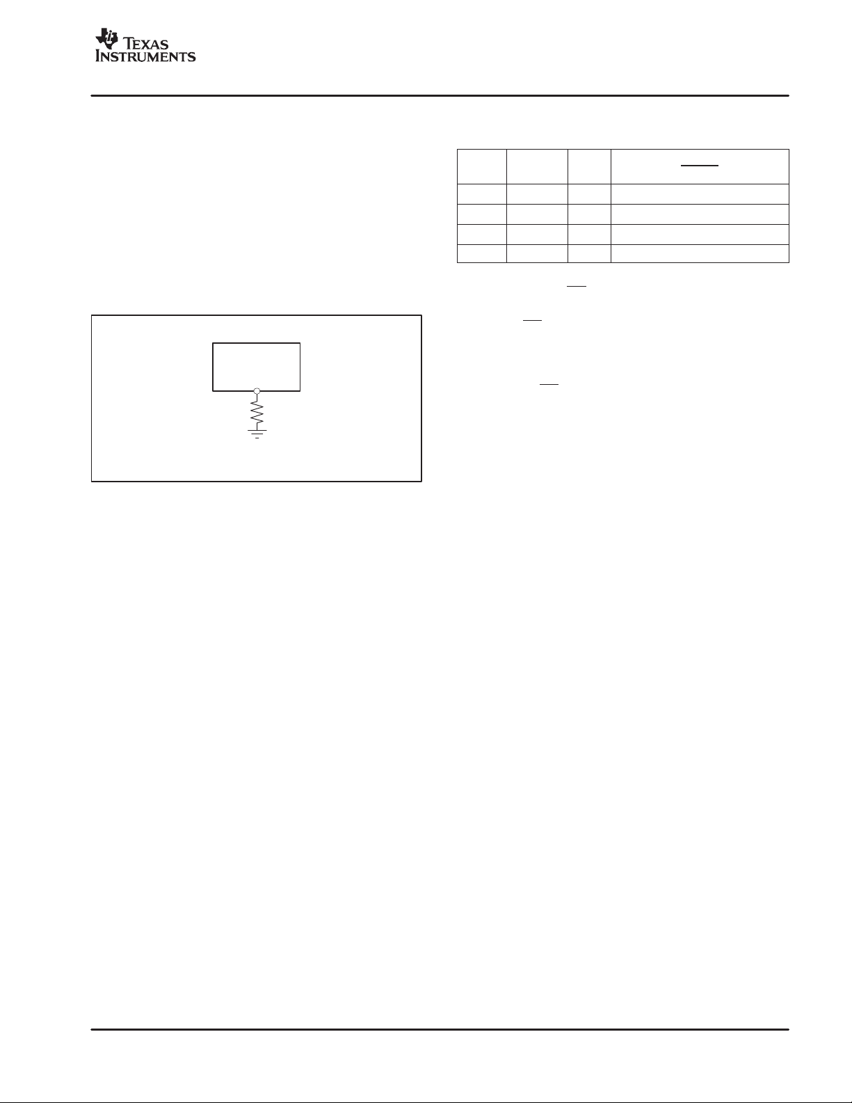
ANALOG POWER DISSIPATION
An external resistor connected between the RBIAS pin
and the analog ground sets the analog current level, as
shown in Figure 52. The current is inversely proportional
to the resistor value. Table 3 shows the recommended
values of R
for different CLK frequencies. Notice that
BIAS
the analog current can be reduced when using a slower
frequency CLK input because the modulator has more
time to settle. Avoid adding any capacitance in parallel to
R
, since this will interfere with the internal circuitry
BIAS
used to set the biasing.
ADS1602
RBIAS
R
BIAS
AGND
Figure 52. External Resistor Used to Set Analog
Power Dissipation
Table 3. Recommended R
Different CLK Frequencies
DATA
f
CLK
16MHz 1MHz 140kΩ 200mW
24MHz 1.5MHz 100kΩ 270mW
32MHz 2MHz 60kΩ 390mW
40MHz 2.5MHz 37kΩ 530mW
RATE
R
BIAS
Resistor Values for
BIAS
TYPICAL POWER DISSIPATION
WITH REFEN HIGH
POWER DOWN (PD)
When not in use, the ADS1602 can be powered down by
taking the PD
pin low. All circuitry will be shut down,
including the voltage reference. To minimize the digital
current during power down, stop the clock signal supplied
to the CLK input. There is an internal pull-up resistor of
170kΩ on the PD
pin, but it is recommended that this pin
be connected to IOVDD if not used. Make sure to allow
time for the reference to start up after exiting power-down
mode. The internal reference typically requires 15ms.
After the reference has stabilized, allow at least 100
conversions for the modulator and digital filter to settle
before retrieving data.
21
Page 22

"#$%&
SBAS341B − DECEMBER 2004 − REVISED APRIL 2005
www.ti.com
POWER SUPPLIES
Three supplies are used on the ADS1602: analog (AVDD),
digital (DVDD) and digital I/O (IOVDD). Each supply must
be suitably bypassed to achieve the best performance. It
is recommended that a 1µF and 0.1µF ceramic capacitor
be placed as close to each supply pin as possible. Connect
each supply-pin bypass capacitor to the associated
DVDD
47µF4.7µF1µF0.1µF
IOVDD
47µF
AVDD
47µF
4.7µF
4.7µF
If using separate analog and
digital ground planes, connect
together on the ADS1602 PCB.
1µF
1µF
0.1µF
0.1µF
1 36DGND
C
P
2
3
6
ground, as shown in Figure 53. Each main supply bus
should also be bypassed with a bank of capacitors from
47µF to 0.1µF, as shown.
The I/O and digital supplies (IOVDD and DVDD) can be
connected together when using the same voltage. In this
case, only o n e b a n k o f 4 7 µF to 0.1µF capacitors is needed
on the main supply bus, though each supply pin must still
be bypassed with a 1µF and 0.1µF ceramic capacitor.
C
P
42 41 55 38 37 34 33
AGND
AVDD
AGND
AVDD
AGND
C
P
AGND
DGND
C
P
DVDD
IOVDD
DGND
DGND
AGND
NOTE: CP=1µF0.1µF
Figure 53. Recommended Power-Supply Bypassing
C
P
AVDD
7
9
AGND
C
P
AVDD
10
11
AGND
C
P
12
AVDD
RPULLUP
15
18
Ω
10k
ADS1602
DVDD
DGND
19 22 23
C
P
DGND
DVDD
C
P
22
Page 23

www.ti.com
"#$%&
SBAS341B − DECEMBER 2004 − REVISED APRIL 2005
LAYOUT ISSUES AND COMPONENT SELECTION
The ADS1602 is a very high-speed, high-resolution data
converter. In order to achieve maximum performance, the
user must give very careful consideration to both the layout
of the printed circuit board (PCB) in addition to the routing
of the traces. Capacitors that are critical to achieve the
best performance from the device should be placed as
close to the pins of the device as possible. These include
capacitors related the analog inputs, the reference and the
power supplies.
For critical capacitors, it is recommended that Class II
dielectrics such as Z5U be avoided. These dielectrics
have a narrow operating temperature, a large tolerance on
the capacitance and will lose up to 20% of the rated
capacitance over 10,000 hours. Rather, select capacitors
with a Class I dielectric. C0G (also known as NP0), for
example, has a tight tolerance < ±30PPM/°C and is very
stable over time. Should Class II capacitors be chosen
because of the size constraints, select an X7R or X5R
dielectric to minimize the variations of the capacitor’s
critical characteristics.
The resistors used in the circuits driving the input and
reference should be kept as low as possible to prevent
excess thermal noise from degrading the system
performance.
The digital outputs from the device should always be
buffered. This will have a number of benefits: it will reduce
the loading of the internal digital buffers, which decreases
noise generated within the device, and it will also reduce
device power consumption.
The McBSP provides a host of functions including:
D Full-duplex communication
D Double-buffered data registers
D Independent framing and clocking for reception and
transmission of data
The sequence begins with a one-time synchronization of
the serial port by the microprocessor. The ADS1602
recognizes the SYNC signal if it is high for a least 1 CLK
period. Transfers are initiated by the ADS1602 after the
SYNC signal is de-asserted by the microprocessor.
The FSO signal from the ADS1602 indicates that data is
available to be read, and is connected to the Frame Sync
Receive (FSR) pin of the DSP. The Clock Receiver (CLKR)
is derived directly from the ADS1602 serial clock output to
ensure continued synchronization of data with the clock.
ADS1602
FSO
SCLK
DOUT
SYNC
TMS320
FSR
CLKR
DR
FSX
APPLICATIONS INFORMATION
Interfacing the ADS1602 to the TMS320 DSP family.
Since the ADS1602 communicates with the host via a
serial interface, the most suitable method to connect to any
of the TMS320 DSPs is via the Multi-channel Buffered
Serial Port (McBSP). A typical connection to the TMS320
DSP is shown in Figure 54.
Figure 54. ADS1602—TMS320 Interface
Connection
An Evaluation Module (EVM) is available from Texas
Instruments. The module consists of the ADS1602 and
supporting circuits, allowing users to quickly assess the
performance and characteristics of the ADS1602. The
EVM easily connects to various microcontrollers and DSP
systems. For more details, or to download a copy of the
ADS1602EVM User’s Guide, visit the Texas Instruments
web site at www.ti.com.
23
Page 24
PACKAGE OPTION ADDENDUM
www.ti.com
19-Apr-2005
PACKAGING INFORMATION
Orderable Device Status
(1)
Package
Type
Package
Drawing
Pins Package
Qty
Eco Plan
ADS1602IPFBR ACTIVE TQFP PFB 48 1000 Green (RoHS &
no Sb/Br)
ADS1602IPFBRG4 ACTIVE TQFP PFB 48 1000 Green (RoHS &
no Sb/Br)
ADS1602IPFBT ACTIVE TQFP PFB 48 250 Green (RoHS &
no Sb/Br)
ADS1602IPFBTG4 ACTIVE TQFP PFB 48 250 Green (RoHS &
no Sb/Br)
(1)
The marketing status values are defined as follows:
ACTIVE: Product device recommended for new designs.
LIFEBUY: TI has announced that the device will be discontinued, and a lifetime-buy period is in effect.
NRND: Not recommended for new designs. Device is in production to support existing customers, but TI does not recommend using this part in
a new design.
PREVIEW: Device has been announced but is not in production. Samples may or may not be available.
OBSOLETE: TI has discontinued the production of the device.
(2)
Eco Plan - The planned eco-friendly classification: Pb-Free (RoHS) or Green (RoHS & no Sb/Br) - please check
http://www.ti.com/productcontent for the latest availability information and additional product content details.
TBD: The Pb-Free/Green conversion plan has not been defined.
Pb-Free (RoHS): TI's terms "Lead-Free" or "Pb-Free" mean semiconductor products that are compatible with the current RoHS requirements
for all 6 substances, including the requirement that lead not exceed 0.1% by weight in homogeneous materials. Where designed to be soldered
at high temperatures, TI Pb-Free products are suitable for use in specified lead-free processes.
Green (RoHS & no Sb/Br): TI defines "Green" to mean Pb-Free (RoHS compatible), and free of Bromine (Br) and Antimony (Sb) based flame
retardants (Br or Sb do not exceed 0.1% by weight in homogeneous material)
(2)
Lead/Ball Finish MSL Peak Temp
CU NIPDAU Level-2-260C-1 YEAR
CU NIPDAU Level-2-260C-1 YEAR
CU NIPDAU Level-2-260C-1 YEAR
CU NIPDAU Level-2-260C-1 YEAR
(3)
(3)
MSL, Peak Temp. -- The Moisture Sensitivity Level rating according to the JEDEC industry standard classifications, and peak solder
temperature.
Important Information and Disclaimer:The information provided on this page represents TI's knowledge and belief as of the date that it is
provided. TI bases its knowledge and belief on information provided by third parties, and makes no representation or warranty as to the
accuracy of such information. Efforts are underway to better integrate information from third parties. TI has taken and continues to take
reasonable steps to provide representative and accurate information but may not have conducted destructive testing or chemical analysis on
incoming materials and chemicals. TI and TI suppliers consider certain information to be proprietary, and thus CAS numbers and other limited
information may not be available for release.
In no event shall TI's liability arising out of such information exceed the total purchase price of the TI part(s) at issue in this document sold by TI
to Customer on an annual basis.
Addendum-Page 1
Page 25

MECHANICAL DATA
MTQF019A – JANUARY 1995 – REVISED JANUARY 1998
PFB (S-PQFP-G48) PLASTIC QUAD FLATPACK
37
48
1,05
0,95
0,50
36
0,27
0,17
25
24
13
1
5,50 TYP
7,20
SQ
6,80
9,20
SQ
8,80
12
M
0,08
0,05 MIN
Seating Plane
0,13 NOM
Gage Plane
0,25
0°–7°
0,75
0,45
1,20 MAX
NOTES: A. All linear dimensions are in millimeters.
B. This drawing is subject to change without notice.
C. Falls within JEDEC MS-026
0,08
4073176/B 10/96
POST OFFICE BOX 655303 • DALLAS, TEXAS 75265
Page 26

IMPORTANT NOTICE
Texas Instruments Incorporated and its subsidiaries (TI) reserve the right to make corrections, modifications,
enhancements, improvements, and other changes to its products and services at any time and to discontinue
any product or service without notice. Customers should obtain the latest relevant information before placing
orders and should verify that such information is current and complete. All products are sold subject to TI’s terms
and conditions of sale supplied at the time of order acknowledgment.
TI warrants performance of its hardware products to the specifications applicable at the time of sale in
accordance with TI’s standard warranty. Testing and other quality control techniques are used to the extent TI
deems necessary to support this warranty . Except where mandated by government requirements, testing of all
parameters of each product is not necessarily performed.
TI assumes no liability for applications assistance or customer product design. Customers are responsible for
their products and applications using TI components. To minimize the risks associated with customer products
and applications, customers should provide adequate design and operating safeguards.
TI does not warrant or represent that any license, either express or implied, is granted under any TI patent right,
copyright, mask work right, or other TI intellectual property right relating to any combination, machine, or process
in which TI products or services are used. Information published by TI regarding third-party products or services
does not constitute a license from TI to use such products or services or a warranty or endorsement thereof.
Use of such information may require a license from a third party under the patents or other intellectual property
of the third party, or a license from TI under the patents or other intellectual property of TI.
Reproduction of information in TI data books or data sheets is permissible only if reproduction is without
alteration and is accompanied by all associated warranties, conditions, limitations, and notices. Reproduction
of this information with alteration is an unfair and deceptive business practice. TI is not responsible or liable for
such altered documentation.
Resale of TI products or services with statements different from or beyond the parameters stated by TI for that
product or service voids all express and any implied warranties for the associated TI product or service and
is an unfair and deceptive business practice. TI is not responsible or liable for any such statements.
Following are URLs where you can obtain information on other Texas Instruments products and application
solutions:
Products Applications
Amplifiers amplifier.ti.com Audio www.ti.com/audio
Data Converters dataconverter.ti.com Automotive www.ti.com/automotive
DSP dsp.ti.com Broadband www.ti.com/broadband
Interface interface.ti.com Digital Control www.ti.com/digitalcontrol
Logic logic.ti.com Military www.ti.com/military
Power Mgmt power.ti.com Optical Networking www.ti.com/opticalnetwork
Microcontrollers microcontroller.ti.com Security www.ti.com/security
Telephony www.ti.com/telephony
Video & Imaging www.ti.com/video
Wireless www.ti.com/wireless
Mailing Address: Texas Instruments
Post Office Box 655303 Dallas, Texas 75265
Copyright 2005, Texas Instruments Incorporated
 Loading...