

Page 1
Control
CLK
GPIOANDCONTROL
Oscillator
SPI
TestSignalsand
Monitors
PACE
SPI
RLD
Wilson
Terminal
WCT
Reference
REF
ADC7
ADC8
ADC1
ADC2
ADC3
ADC4
ADC5
ADC6
A7
A8
A1
A2
A3
A4
A5
A6
MUX
INPUTS
¼ ¼
¼
ToChannel
RESP
Resp
RESP
DEMOD
ADS129xR
ADS129xR
www.ti.com.cn
ADS1294, ADS1294R
ADS1296, ADS1296R
ADS1298, ADS1298R
ZHCS313I –JANUARY 2010– REVISED JANUARY 2012
用于生物电位测量的低功率,
查询样品
1
特性
23
• 8个低噪音PGA和8个高分辨率ADC(ADS1298,
ADS1298R)
• 低功耗:每通道 0.75 mW
• 输入参考噪声:4μVPP(150Hz BW, G = 6)
• 输入偏置电流:200pA
• 数据速率:250SPS至32kSPS
• CMRR:–115dB
• 可编程增益:1,2,3,4,6,8或者12
• 支持AAMI
EC11,EC13,IEC60601-1,IEC60601-2-27,
和IEC60601-2-51标准
• 单极或双极电源:
AVDD = 2.7V至5.25V,DVDD = 1.65V至3.6V
• 内置右腿驱动放大器,检测,WCT,PACE检测,
测试信号
• 集成的呼吸阻抗测量(只适用
于ADS1294R/6R/8R)
• 数字PACE检测功能
• 内置振荡器与参考
• 灵活的断电,待机模式
• 串行外设接口(SPI)™- 兼容串口
• 运行温度范围:
–40°C至+85°C
: ADS1294, ADS1294R, ADS1296, ADS1296R, ADS1298, ADS1298R
8通道,24位模拟前端
借助于其高水平的集成和出色的性
能,ADS1294/6/8/4R/6R/8R系列产品可以用大大减小
的尺寸,功率,和总体成本来开发可扩展的医疗仪器。
ADS1294/6/8/4R/6R/8R在每通道上有一个灵活输入复
用器,此复用器可独立连接至用于测试,温度,和持续
断线检测的内部生成信号。 此外,可选择输入通道的
各种配置生成右腿驱动器 (RLD) 输出信号。
ADS1294/6/8/4R/6R/8R运行数据速率最高可
达32KSPS,因此可实现软件PACE检测。 可通过上
拉/下拉电阻器或激磁电流源极/汲极为该器件内部实
施持续断线检测。 3个集成的放大器生成标准12引
线ECG所需的威尔逊(Wilson)中心终端(WCT)和高德伯
格(Goldberger)中心终端(GCT)。 ADS1294R/6R/8R版
本包括一个完全集成的,呼吸阻抗测量功能。
多个ADS1294/6/8/4R/6R/8R器件可使用菊花链配置级
联在高通道数量系统中。
封装选项包括微小型 8mm × 8mm ,64焊球 BGA
与TQFP-64封装。 ADS1294/6/8 BGA版本商用额定温
度范围为0°C至+70°C。 ADS1294R/6R/8R BGA
和ADS1294/6/8 TQFP版本工业用额定温度范围
是–40°C至+85°C。
应用范围
• 医疗仪器(ECG,EMG和EEG)
病人监护:动态心电图,事件,压力,和包
括ECG,AED在内的重要生命体征信号,远程医疗
双谱指数(BIS),诱发音频电位(EAP),睡眠监护仪
• 高精度,同步,多通道信号采集
说明
ADS1294/6/8/4R/6R/8R是多通道,同步采样,24位,
三角积分(ΔΣ)模数转换器(ADC)系列产品,此产品具有
内置的可编程增益放大器(PGA),内部基准,和一个板
载振荡器。 ADS1294/6/8/4R/6R/8R包含了所有医疗心
电图(ECG)和脑电图(EEG)应用所通常要求的所有特
性。
1
2串行外设接口(SPI) is a trademark of Motorola.
3All other trademarks are the property of their respective owners.
PRODUCTION DATA information is current as of publication date.
Products conform to specifications per the terms of the Texas
Instruments standard warranty. Production processing does not English Data Sheet: SBAS459
necessarily include testing of all parameters.
Please be aware that an important notice concerning availability, standard warranty, and use in critical applications of Texas
Instruments semiconductor products and disclaimers thereto appears at the end of this data sheet.
Copyright © 2010–2012, Texas Instruments Incorporated
Page 2

ADS1294, ADS1294R
ADS1296, ADS1296R
ADS1298, ADS1298R
ZHCS313I –JANUARY 2010– REVISED JANUARY 2012
This integrated circuit can be damaged by ESD. Texas Instruments recommends that all integrated circuits be handled with
appropriate precautions. Failure to observe proper handling and installation procedures can cause damage.
ESD damage can range from subtle performance degradation to complete device failure. Precision integrated circuits may be more
susceptible to damage because very small parametric changes could cause the device not to meet its published specifications.
www.ti.com.cn
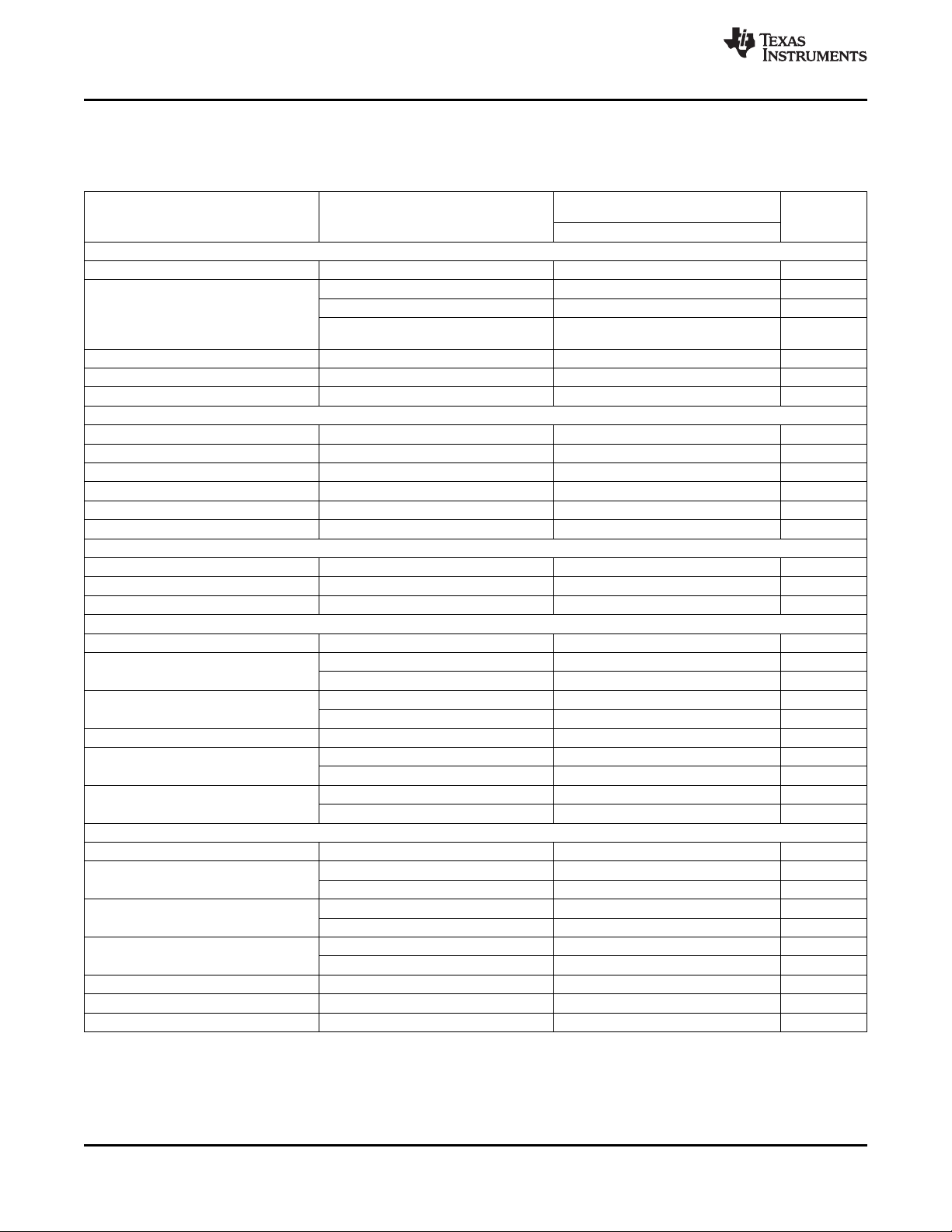
FAMILY AND ORDERING INFORMATION
PRODUCT OPTION CHANNELS RESOLUTION (kSPS) RANGE CIRCUITRY
ADS1194
ADS1196
ADS1198
ADS1294 BGA 4 24 32 0°C to +70°C External
ADS1294R BGA 4 24 32 –40°C to +85°C Yes
ADS1294 TQFP 4 24 32 –40°C to +85°C External
ADS1296 BGA 6 24 32 0°C to +70°C External
ADS1296R BGA 6 24 32 –40°C to +85°C Yes
ADS1296 TQFP 6 24 32 –40°C to +85°C External
ADS1298 BGA 8 24 32 0°C to +70°C External
ADS1298R BGA 8 24 32 –40°C to +85°C Yes
ADS1298 TQFP 8 24 32 –40°C to +85°C External
(1) For the most current package and ordering information, see the Package Option Addendum at the end of this document, or visit the
device product folder at www.ti.com.
ABSOLUTE MAXIMUM RATINGS
PACKAGE NUMBER OF ADC SAMPLE RATE TEMPERATURE RESPIRATION
BGA 4 16 8 0°C to +70°C No
TQFP 4 16 8 0°C to +70°C No
BGA 6 16 8 0°C to +70°C No
TQFP 6 16 8 0°C to +70°C No
BGA 8 16 8 0°C to +70°C No
TQFP 8 16 8 0°C to +70°C No
(1)
MAXIMUM OPERATING
(1)
Over operating free-air temperature range, unless otherwise noted.
ADS1294, ADS1296, ADS1298
ADS1294R, ADS1296R, ADS1298R
AVDD to AVSS –0.3 to +5.5 V
DVDD to DGND –0.3 to +3.9 V
AVSS to DGND –3 to +0.2 V
V
input to AVSS AVSS – 0.3 to AVDD + 0.3 V
REF
Analog input to AVSS AVSS – 0.3 to AVDD + 0.3 V
Digital input voltage to DGND –0.3 to DVDD + 0.3 V
Digital output voltage to DGND –0.3 to DVDD + 0.3 V
Input current (momentary) 100 mA
Input current (continuous) 10 mA
Operating
temperature
range
ESD ratings
Storage temperature range –60 to +150 °C
Maximum junction temperature (TJ) +150 °C
(1) Stresses above these ratings may cause permanent damage. Exposure to absolute maximum conditions for extended periods may
degrade device reliability. These are stress ratings only, and functional operation of the device at these or any other conditions beyond
those specified is not implied.
Commerical Grade: ADS1294, ADS1296, ADS1298 0 to +70 °C
Industrial grade: ADS1294I, ADS1296I, ADS1298I,
ADS1294RI, ADS1296RI, ADS1298RI
Human body model (HBM)
JEDEC standard 22, test method A114-C.01, all pins
Charged device model (CDM)
JEDEC standard 22, test method C101, all pins
–40 to +85 °C
±2000 V
±500 V
UNIT
2 Copyright © 2010–2012, Texas Instruments Incorporated
Page 3
ADS1294, ADS1294R
ADS1296, ADS1296R
ADS1298, ADS1298R
www.ti.com.cn
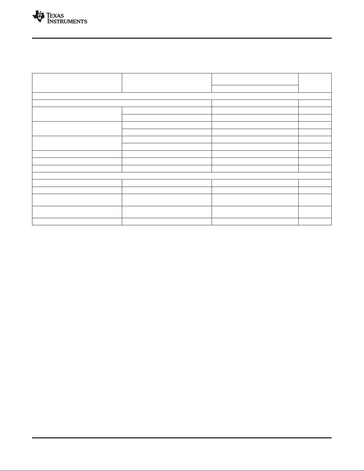
ELECTRICAL CHARACTERISTICS
Minimum/maximum specifications apply for all commercial grade (0°C to +70°C) devices and from –40°C to +85°C for
industrial grades devices. Typical specifications are at +25°C. All specifications at DVDD = 1.8V, AVDD – AVSS = 3V
V
= 2.4V, external f
REF
PARAMETER TEST CONDITIONS MIN TYP MAX UNIT
ANALOG INPUTS
Full-scale differential input voltage (AINP – AINN) ±V
Input common-mode range subsection of the PGA Settings and Input
Input capacitance 20 pF
Input bias current TA= 0°C to +70°C, input = 1.5V ±1 nA
DC input impedance Current source lead-off detection 500 MΩ
PGA PERFORMANCE
Gain settings 1, 2, 3, 4, 6, 8, 12
Bandwidth See Table 6
ADC PERFORMANCE
Resolution 16kSPS data rate 19 Bits
Data rate
CHANNEL PERFORMANCE
DC Performance
Input-referred noise
Integral nonlinearity ADS1294R/6R/8R channel 1
Offset error ±500 µV
Offset error drift 2 µV/°C
Gain error Excluding voltage reference error ±0.2 ±0.5 % of FS
Gain drift Excluding voltage reference drift 5 ppm/°C
Gain match between channels 0.3 % of FS
(1) Performance is applicable for 5V operation as well. Production testing for limits is performed at 3V.
(2) Noise data measured in a 10-second interval. Test not performed in production. Input-referred noise is calculated with input shorted
(without electrode resistance) over a 10-second interval.
= 2.048MHz, data rate = 500SPS, High-Resolution mode, and gain = 6, unless otherwise noted.
CLK
TA= +25°C, input = 1.5V ±200 pA
TA= –40°C to +85°C, input = 1.5V ±1.2 nA
No lead-off 1000 MΩ
Pull-up resistor lead-off detection 10 MΩ
Data rates up to 8kSPS, no missing codes 24 Bits
32kSPS data rate 17 Bits
f
= 2.048MHz, High-Resolution mode 500 32000 SPS
CLK
f
= 2.048MHz, Low-Power mode 250 16000 SPS
CLK
(2)
Gain = 6
Gain = 6, 256 points, 0.5 seconds of data 4 7 μV
Gain settings other than 6, data rates other
than 500SPS
Full-scale with gain = 6, best fit 8 ppm
Full-scale with gain = 6, best fit,
–20dBFS with gain = 6, best fit,
ADS1294R/6R/8R channel 1
, 10 seconds of data 5 μV
ZHCS313I –JANUARY 2010– REVISED JANUARY 2012
(1)
ADS1294, ADS1296, ADS1298
ADS1294R, ADS1296R, ADS1298R
/GAIN V
REF
See the Input Common-Mode Range
Range section
See Noise Measurements section
40 ppm
8 ppm
,
PP
PP
Copyright © 2010–2012, Texas Instruments Incorporated 3
Page 4
ADS1294, ADS1294R
ADS1296, ADS1296R
ADS1298, ADS1298R
ZHCS313I –JANUARY 2010– REVISED JANUARY 2012
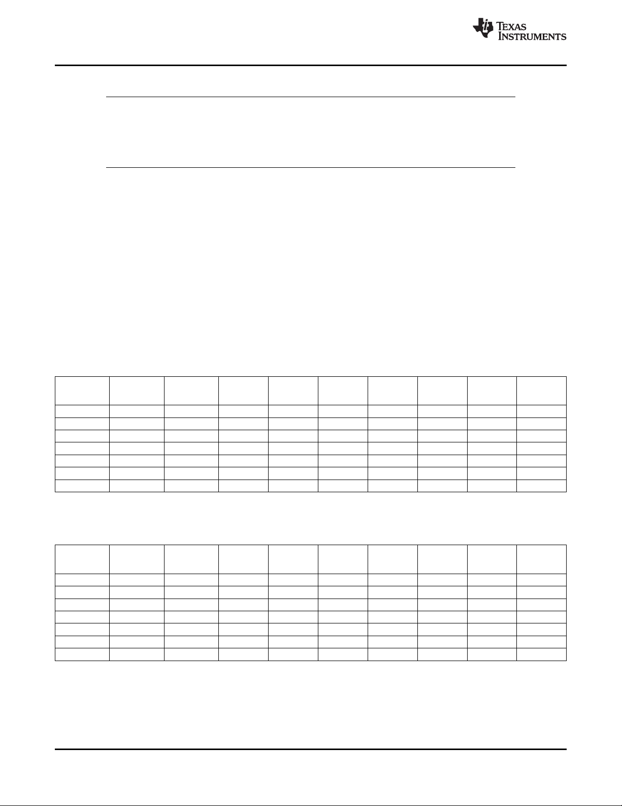
ELECTRICAL CHARACTERISTICS (continued)
Minimum/maximum specifications apply for all commercial grade (0°C to +70°C) devices and from –40°C to +85°C for
industrial grades devices. Typical specifications are at +25°C. All specifications at DVDD = 1.8V, AVDD – AVSS = 3V
V
= 2.4V, external f
REF
PARAMETER TEST CONDITIONS MIN TYP MAX UNIT
CHANNEL PERFORMANCE (continued)
AC Performance
Common-mode rejection ratio (CMRR) fCM= 50Hz, 60Hz
Power-supply rejection ratio (PSRR) fPS= 50Hz, 60Hz 90 dB
Crosstalk fIN= 50Hz, 60Hz –126 dB
Signal-to-noise ratio (SNR) fIN= 10Hz input, gain = 6 112 dB
Total harmonic distortion (THD)
DIGITAL FILTER
–3dB bandwidth 0.262f
Digital filter settling Full setting 4 Conversions
RIGHT LEG DRIVE (RLD) AMPLIFIER AND PACE AMPLIFIERS
RLD integrated noise BW = 150Hz 7 μV
PACE integrated noise BW = 8kHz 20 µV
PACE amplifier crosstalk Crosstalk between PACE amplifiers 60 dB
Gain bandwidth product 50kΩ || 10pF load, gain = 1 100 kHz
Slew rate 50kΩ || 10pF load, gain = 1 0.25 V/μs
PACE and RLD amplifier drive strength
PACE and RLD current
PACE amplifier output resistance 100 Ω
Total harmonic distortion fIN= 100Hz, gain = 1 –70 dB
Common-mode input range AVSS + 0.7 AVDD – 0.3 V
Common-mode resistor matching Internal 200kΩ resistor matching 0.1 %
Short-circuit current ±0.25 mA
Quiescent power consumption Either RLD or PACE amplifier 20 μA
WILSON CENTRAL TERMINAL (WCT) AMPLIFIER
Integrated noise BW = 150Hz See Table 5 nV/√Hz
Gain bandwidth product See Table 5 kHz
Slew rate See Table 5 V/s
Total harmonic distortion fIN= 100Hz 90 dB
Common-mode input range AVSS + 0.3 AVDD – 0.3 V
Short-circuit current Through internal 30kΩ resistor ±0.25 mA
Quiescent power consumption See Table 5 μA
(3) CMRR is measured with a common-mode signal of AVSS + 0.3V to AVDD – 0.3V. The values indicated are the maximum of the eight
channels.
(4) Harmonics above the second harmonic are attenuated by the digital filter.
= 2.048MHz, data rate = 500SPS, High-Resolution mode, and gain = 6, unless otherwise noted.
CLK
ADS1294, ADS1296, ADS1298
ADS1294R, ADS1296R, ADS1298R
(3)
10Hz, –0.5dBFs –98 dB
ADS1294R/6R/8R channel 1, 10Hz, –0.5dBFs –70 dB
100Hz, –0.5dBFs
ADS1294R/6R/8R channel 1,
100Hz, –0.5dBFs
ADS1294R/6R/8R channel 1,
100Hz, –20dBFs
Short-circuit to GND (AVDD = 3V) 270 μA
Short-circuit to supply (AVDD = 3V) 550 μA
Short-circuit to GND (AVDD = 5V) 490 μA
Short-circuit to supply (AVDD = 5V) 810 μA
Peak swing (AVSS + 0.3V to AVDD + 0.3V)
at AVDD = 3V
Peak swing (AVSS + 0.3V to AVDD + 0.3V)
at AVDD = 5V
(4)
(4)
(4)
–105 –115 dB
–100 dB
–68 dB
–86 dB
DR
50 μA
75 μA
www.ti.com.cn
(1)
,
Hz
RMS
RMS
4 Copyright © 2010–2012, Texas Instruments Incorporated
Page 5
ADS1294, ADS1294R
ADS1296, ADS1296R
ADS1298, ADS1298R
www.ti.com.cn
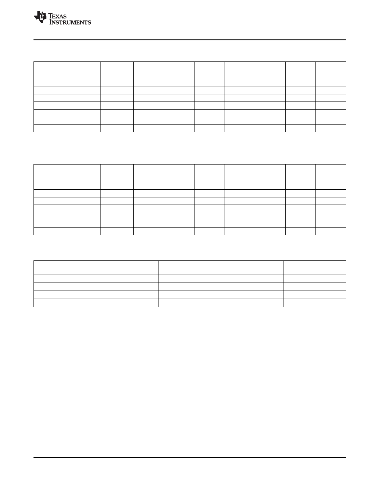
ELECTRICAL CHARACTERISTICS (continued)
Minimum/maximum specifications apply for all commercial grade (0°C to +70°C) devices and from –40°C to +85°C for
industrial grades devices. Typical specifications are at +25°C. All specifications at DVDD = 1.8V, AVDD – AVSS = 3V
V
= 2.4V, external f
REF
PARAMETER TEST CONDITIONS MIN TYP MAX UNIT
LEAD-OFF DETECT
Frequency See the Register Map section for settings 0, fDR/4 kHz
Current See the Register Map section for settings 6, 12, 18, 24 nA
Current accuracy ±20 %
Comparator threshold accuracy ±30 mV
RESPIRATION (ADS1294R/6R/8R Only)
Frequency
Phase shift See the Register Map section for settings 22.5 90 157.5 Degrees
Impedance range I
Impedance measurement noise 20 mΩ
Modulator current 29 µA
EXTERNAL REFERENCE
Reference input voltage
Negative input (VREFN) AVSS V
Positive input (VREFP) AVSS + 2.5 V
Input impedance 10 kΩ
INTERNAL REFERENCE
Output voltage
V
accuracy ±0.2 %
REF
Internal reference drift Commerical grade, 0°C to +70°C 35 ppm
Start-up time 150 ms
SYSTEM MONITORS
Analog supply reading error 2 %
Digital supply reading error 2 %
Device wake up
Temperature sensor reading, voltage TA= +25°C 145 mV
Temperature sensor reading, coefficient 490 μV/°C
Test Signal
Signal frequency See Register Map section for settings Hz
Signal voltage See Register Map section for settings ±1, ±2 mV
Accuracy ±2 %
= 2.048MHz, data rate = 500SPS, High-Resolution mode, and gain = 6, unless otherwise noted.
CLK
Internal source 32, 64 kHz
External source 32 64 kHz
= 30μA 10 kΩ
RESP
0.05Hz to 2Hz brick wall filter, 32kHz
modulation clock, phase = 112.5,
using I
gain = 4 test condition
internal reference, signal path = 82kΩ,
baseline = 2.21kΩ
3V supply V
5V supply V
Register bit CONFIG3.VREF_4V = 0,
AVDD ≥ 2.7V
Register bit CONFIG3.VREF_4V = 1,
AVDD ≥ 4.4V
TA= +25°C 35 ppm/°C
Industrial grade, –40°C to +85°C 45 ppm
From power-up to DRDY low 150 ms
STANDBY mode 9 ms
= 30μA with 2kΩ baseline load,
RESP
= (VREFP – VREFN) 2.5 V
REF
= (VREFP – VREFN) 4.0 V
REF
ZHCS313I –JANUARY 2010– REVISED JANUARY 2012
ADS1294, ADS1296, ADS1298
ADS1294R, ADS1296R, ADS1298R
2.4 V
4.0 V
CLK
20
/2
f
/221, f
CLK
(1)
,
PP
Copyright © 2010–2012, Texas Instruments Incorporated 5
Page 6
ADS1294, ADS1294R
ADS1296, ADS1296R
ADS1298, ADS1298R
ZHCS313I –JANUARY 2010– REVISED JANUARY 2012
ELECTRICAL CHARACTERISTICS (continued)
Minimum/maximum specifications apply for all commercial grade (0°C to +70°C) devices and from –40°C to +85°C for
industrial grades devices. Typical specifications are at +25°C. All specifications at DVDD = 1.8V, AVDD – AVSS = 3V
V
= 2.4V, external f
REF
PARAMETER TEST CONDITIONS MIN TYP MAX UNIT
CLOCK
Internal oscillator clock frequency Nominal frequency 2.048 MHz
Internal clock accuracy
Internal oscillator start-up time 20 μs
Internal oscillator power consumption 120 μW
External clock input frequency CLKSEL pin = 0 1.94 2.048 2.25 MHz
DIGITAL INPUT/OUTPUT (DVDD = 1.65V to 3.6V)
Logic level
V
IH
V
IL
V
OH
V
OL
Input current (IIN) 0V < V
POWER-SUPPLY REQUIREMENTS
Analog supply (AVDD – AVSS) 2.7 3.0 5.25 V
Digital supply (DVDD) 1.65 1.8 3.6 V
AVDD – DVDD –2.1 3.6 V
SUPPLY CURRENT (RLD, WCT, and PACE Amplifiers Turned Off)
High-Resolution mode (ADS1298)
I
AVDD
I
DVDD
Low-Power mode (ADS1298)
I
AVDD
I
DVDD
POWER DISSIPATION (Analog Supply = 3V, RLD, WCT, and PACE Amplifiers Turned Off)
Quiescent power dissipation
ADS1298/8R
ADS1296/6R
ADS1294/4R
Power-down 10 μW
Standby mode 2 mW
Quiescent channel power PGA + ADC 818 μW
= 2.048MHz, data rate = 500SPS, High-Resolution mode, and gain = 6, unless otherwise noted.
CLK
ADS1294, ADS1296, ADS1298
ADS1294R, ADS1296R, ADS1298R
TA= +25°C ±0.5 %
0°C ≤ TA≤ +70°C ±2 %
–40°C ≤ TA≤ +85°C,
ADS1298I industrial grade version only
0.8DVDD DVDD + 0.1 V
–0.1 0.2DVDD V
IOH= –500μA DVDD – 0.4 V
IOL= +500μA 0.4 V
< DVDD –10 +10 μA
DigitalInput
AVDD – AVSS = 3V 2.75 mA
AVDD – AVSS = 5V 3.1 mA
DVDD = 3.0V 0.5 mA
DVDD = 1.8V 0.3 mA
AVDD – AVSS = 3V 1.8 mA
AVDD – AVSS = 5V 2.1 mA
DVDD = 3.0V 0.5 mA
DVDD = 1.8V 0.3 mA
High-Resolution mode 8.8 9.5 mW
Low-Power mode (250SPS) 6.0 7.0 mW
High-Resolution mode 7.2 7.9 mW
Low-Power mode 5.3 6.6 mW
High-Resolution mode 5.4 6 mW
Low-Power mode 4.1 4.4 mW
www.ti.com.cn
±2.5 %
(1)
,
6 Copyright © 2010–2012, Texas Instruments Incorporated
Page 7
ADS1294, ADS1294R
ADS1296, ADS1296R
ADS1298, ADS1298R
www.ti.com.cn
ELECTRICAL CHARACTERISTICS (continued)
Minimum/maximum specifications apply for all commercial grade (0°C to +70°C) devices and from –40°C to +85°C for
industrial grades devices. Typical specifications are at +25°C. All specifications at DVDD = 1.8V, AVDD – AVSS = 3V
V
= 2.4V, external f
REF
PARAMETER TEST CONDITIONS MIN TYP MAX UNIT
POWER DISSIPATION (Analog Supply = 5V, RLD, WCT, and PACE Amplifiers Turned Off)
Quiescent power dissipation
ADS1298/8R
ADS1296/6R
ADS1294/4R
Power-down 20 μW
Standby mode 4 mW
Quiescent channel power PGA + ADC 1.5 mW
TEMPERATURE
Specified temperature range 0 +70 °C
Operating temperature range 0 +70 °C
Specified temperature range
(industrial grade only)
Operating temperature range
(industrial grade only)
Storage temperature range –60 +150 °C
= 2.048MHz, data rate = 500SPS, High-Resolution mode, and gain = 6, unless otherwise noted.
CLK
High-Resolution mode 17.5 mW
Low-Power mode 12.5 mW
High-Resolution mode 14.1 mW
Low-Power mode 10 mW
High-Resolution mode 10.1 mW
Low-Power mode 8.3 mW
ZHCS313I –JANUARY 2010– REVISED JANUARY 2012
ADS1294, ADS1296, ADS1298
ADS1294R, ADS1296R, ADS1298R
–40 +85 °C
–40 +85 °C
(1)
,
Copyright © 2010–2012, Texas Instruments Incorporated 7
Page 8
ADS1294, ADS1294R
ADS1296, ADS1296R
ADS1298, ADS1298R
ZHCS313I –JANUARY 2010– REVISED JANUARY 2012
NOISE MEASUREMENTS
NOTE
The ADS1294R/6R/8R channel performance differs from the ADS1294/6/8 in regards to
respiration circuitry found on channel one. Unless otherwise noted, ADS129x refers to all
specifications and functional descriptions of the ADS1294, ADS1296, ADS1298,
ADS1294R, ADS1296R, and ADS1298R.
The ADS129x noise performance can be optimized by adjusting the data rate and PGA setting. As the averaging
is increased by reducing the data rate, the noise drops correspondingly. Increasing the PGA value reduces the
input-referred noise, which is particularly useful when measuring low-level biopotential signals. Table 1 and
Table 2 summarize the noise performance of the ADS129x in the High-Resolution (HR) mode and Low-Power
(LP) mode, respectively, with a 3V analog power supply. Table 3 and Table 4 summarize the noise performance
of the ADS129x in the HR mode and LP mode, respectively, with a 5V analog power supply. The data are
representative of typical noise performance at TA= +25°C. The data shown are the result of averaging the
readings from multiple devices and are measured with the inputs shorted together. A minimum of 1000
consecutive readings are used to calculate the RMS and peak-to-peak noise for each reading. For the two
highest data rates, the noise is limited by quantization noise of the ADC and does not have a gaussian
distribution. Thus, the ratio between rms noise and peak-to-peak noise is approximately 10. For the lower data
rates, the ratio is approximately 6.6.
Table 1 to Table 4 show measurements taken with an internal reference. The data are also representative of the
ADS129x noise performance when using a low-noise external reference such as the REF5025.
www.ti.com.cn
Table 1. Input-Referred Noise (μV
3V Analog Supply and 2.4V Reference
DR BITS OF OUTPUT –3dB
CONFIG1 DATA RATE BANDWIDTH PGA PGA PGA PGA PGA PGA PGA
REGISTER (SPS) (Hz) GAIN = 1 GAIN = 2 GAIN = 3 GAIN = 4 GAIN = 6 GAIN = 8 GAIN = 12
000 32000 8398 335/3553 168/1701 112/1100 85/823 58/529 42.5/378 28.6/248
001 16000 4193 56/613 28/295 18.8/188 14.3/143 9.7/94 7.4/69 5.2/44.3
010 8000 2096 12.4/111 6.5/54 4.5/37.9 3.5/29.7 2.6/21.7 2.2/17.8 1.8/13.8
011 4000 1048 6.1/44.8 3.2/23.3 2.4/17.1 1.9/14.0 1.5/11.1 1.3/9.7 1.2/8.5
100 2000 524 4.1/27.8 2.2/15.4 1.6/11.0 1.3/9.1 1.1/7.3 1.0/6.5 0.9/6.0
101 1000 262 2.9/19.0 1.6/10.1 1.2/7.5 1.0/6.2 0.8/5.0 0.7/4.6 0.6/4.1
110 500 131 2.1/12.5 1.1/6.8 0.9/5.1 0.7/4.3 0.6/3.5 0.5/3.1 0.5/2.9
(1) At least 1000 consecutive readings were used to calculate the RMS and peak-to-peak noise values in this table.
Table 2. Input-Referred Noise (μV
3V Analog Supply and 2.4V Reference
DR BITS OF OUTPUT –3dB
CONFIG1 DATA RATE BANDWIDTH PGA PGA PGA PGA PGA PGA PGA
REGISTER (SPS) (Hz) GAIN = 1 GAIN = 2 GAIN = 3 GAIN = 4 GAIN = 6 GAIN = 8 GAIN = 12
000 16000 4193 333/3481 166/1836 111/1168 84/834 56/576 42/450 28/284
001 8000 2096 56/554 28/272 19/177 14.3/133 9.7/85 7.4/64 5.0/42.4
010 4000 1048 12.5/99 6.5/51 4.5/35.0 3.4/25.9 2.4/18.8 2.0/14.5 1.5/11.3
011 2000 524 6.1/41.8 3.2/22.2 2.3/15.9 1.8/12.1 1.4/9.3 1.2/7.8 1.0/6.7
100 1000 262 4.1/26.3 2.2/14.6 1.6/9.9 1.3/8.1 1.0/6.2 0.8/5.4 0.7/4.7
101 500 131 3.0/17.9 1.6/9.8 1.1/6.8 0.9/5.7 0.7/4.2 0.6/3.6 0.5/3.4
110 250 65 2.1/11.9 1.1/6.3 0.8/4.6 0.7/4.0 0.5/3.0 0.5/2.6 0.4/2.4
(1) At least 1000 consecutive readings were used to calculate the RMS and peak-to-peak noise values in this table.
/μVPP) in High-Resolution Mode
RMS
/μVPP) in Low-Power Mode
RMS
(1)
(1)
8 Copyright © 2010–2012, Texas Instruments Incorporated
Page 9
www.ti.com.cn
ADS1294, ADS1294R
ADS1296, ADS1296R
ADS1298, ADS1298R
ZHCS313I –JANUARY 2010– REVISED JANUARY 2012
Table 3. Input-Referred Noise (μV
5V Analog Supply and 4V Reference
DR BITS OF OUTPUT –3dB
CONFIG1 DATA RATE BANDWIDTH PGA PGA PGA PGA PGA PGA PGA
REGISTER (SPS) (Hz) GAIN = 1 GAIN = 2 GAIN = 3 GAIN = 4 GAIN = 6 GAIN = 8 GAIN = 12
000 32000 8398 521/5388 260/2900 173/1946 130/1403 87/917 65/692 44/483
001 16000 4193 86/1252 43/633 29/402 22/298 15/206 11/141 7/91
010 8000 2096 17/207 9/112 6/71 4/57 3/36 3/29 2/18
011 4000 1048 6.4/48.2 3.4/25.9 2.417.7 1.9/15.4 1.5/11.2 1.3/9.6 1.1/8.2
100 2000 524 4.2/29.9 2.3/15.9 1.6/11.1 1.3/9.3 1.0/7.5 0.9/6.6 0.8/5.8
101 1000 262 2.9/18.8 1.6/10.4 1.1/7.8 0.9/6.1 0.7/4.9 0.6/4.7 0.6/3.9
110 500 131 2.0/12.8 1.1/7.2 0.8/5.2 0.7/4.0 0.5/3.3 0.5/3.3 0.4/2.7
(1) At least 1000 consecutive readings were used to calculate the RMS and peak-to-peak noise values in this table.
Table 4. Input-Referred Noise (μV
5V Analog Supply and 4V Reference
DR BITS OF OUTPUT –3dB
CONFIG1 DATA RATE BANDWIDTH PGA PGA PGA PGA PGA PGA PGA
REGISTER (SPS) (Hz) GAIN = 1 GAIN = 2 GAIN = 3 GAIN = 4 GAIN = 6 GAIN = 8 GAIN = 12
000 16000 4193 526/5985 263/2953 175/1918 132/1410 88/896 66/681 44/458
001 8000 2096 88/1201 44/619 29/411 22/280 15/191 11/139 7/83
010 4000 1048 17/208 9/103 6/62 4/52 3/37 2/25 2/16
011 2000 524 6.0/41.1 3.3/23.3 2.2/15.5 1.8/12.3 1.3/9.8 1.1/7.8 0.9/6.5
100 1000 262 4.1/27.1 2.3/14.8 1.5/10.1 1.2/8.1 0.9/6.0 0.8/5.4 0.7/4.4
101 500 131 2.9/17.4 1.6/9.6 1.1/6.6 0.9/5.9 0.7/4.3 0.6/3.4 0.5/3.2
110 250 65 2.1/11.9 1.1/6.6 0.8/4.6 0.6/3.7 0.5/3.0 0.4/2.5 0.4/2.2
(1) At least 1000 consecutive readings were used to calculate the RMS and peak-to-peak noise values in this table.
/μVPP) in High-Resolution Mode
RMS
/μVPP) in Low-Power Mode
RMS
(1)
(1)
Table 5. Typical WCT Performance
ANY ONE ANY TWO ALL THREE
PARAMETER (A, B, or C) (A+B, A+C, or B+C) (A+B+C) UNIT
Integrated noise 540 382 312 nV
Power 53 59 65 μW
–3dB BW 30 59 89 kHz
Slew rate BW limited BW limited BW limited —
RMS
Copyright © 2010–2012, Texas Instruments Incorporated 9
Page 10
1
2
3
4
5
6
7
8
H
G
F
E
D
C
B
A
IN8P
IN7P
IN6PIN5P
IN4P
IN3P
IN2PIN1P
IN8N
IN7N
IN6NIN5N
IN4N
IN3N
IN2NIN1N
RLDIN
RLDOUT
RLDINV
WCT
TESTP_
PACE_OUT1
TESTN_
PACE_OUT2
VCAP4
VREFP
AVDDAVDDRLDREF
AVSSRESV1
RESP_
MODN
RESP_
MODP
VREFN
AVSSAVSSAVSSAVSS
GPIO4GPIO1
PWDN
VCAP1
AVDDAVDDAVDD
DRDY
GPIO3
DAISY_IN
RESET
VCAP2
AVDD1
VCAP3DGNDDGNDGPIO2
CS
START
DGND
AVSS1
CLKSEL
DVDD
DVDDDOUTSCLKCLK
DIN
ADS1294, ADS1294R
ADS1296, ADS1296R
ADS1298, ADS1298R
ZHCS313I –JANUARY 2010– REVISED JANUARY 2012
(TOP VIEW, SOLDER BUMPS ON BOTTOM SIDE)
www.ti.com.cn
PIN CONFIGURATIONS
ZXG PACKAGE
BGA-64
(1) Connect unused terminals to AVDD.
10 Copyright © 2010–2012, Texas Instruments Incorporated
NAME TERMINAL FUNCTION DESCRIPTION
(1)
IN8P
(1)
IN7P
(1)
IN6P
(1)
IN5P
(1)
IN4P
(1)
IN3P
(1)
IN2P
(1)
IN1P
(1)
IN8N
(1)
IN7N
(1)
IN6N
(1)
IN5N
(1)
IN4N
(1)
IN3N
(1)
IN2N
(1)
IN1N
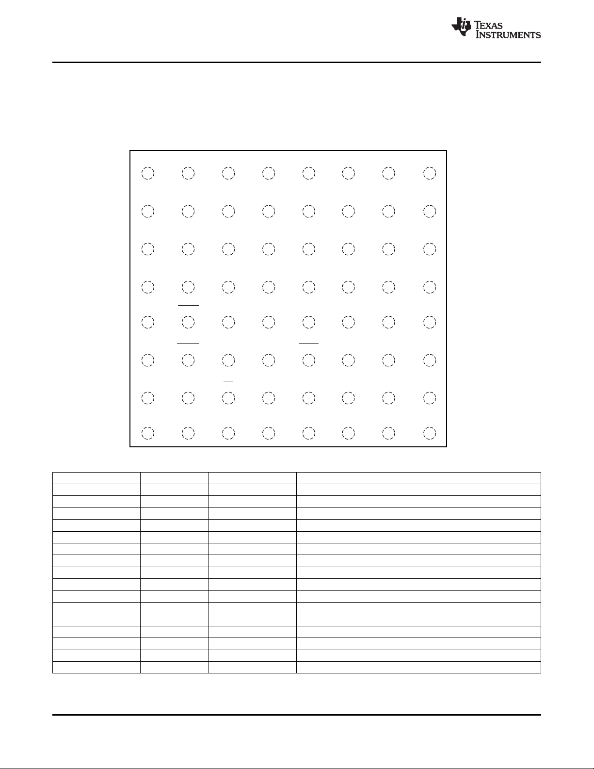
BGA PIN ASSIGNMENTS
1A Analog input Differential analog positive input 8 (ADS1298/8R)
1B Analog input Differential analog positive input 7 (ADS1298/8R)
1C Analog input Differential analog positive input 6 (ADS1296/8/6R/8R)
1D Analog input Differential analog positive input 5 (ADS1296/8/6R/8R)
1E Analog input Differential analog positive input 4
1F Analog input Differential analog positive input 3
1G Analog input Differential analog positive input 2
1H Analog input Differential analog positive input 1
2A Analog input Differential analog negative input 8 (ADS1298/8R)
2B Analog input Differential analog negative input 7 (ADS1298/8R)
2C Analog input Differential analog negative input 6 (ADS1296/8/6R/8R)
2D Analog input Differential analog negative input 5 (ADS1296/8/6R/8R)
2E Analog input Differential analog negative input 4
2F Analog input Differential analog negative input 3
2G Analog input Differential analog negative input 2
2H Analog input Differential analog negative input 1
Page 11

ADS1294, ADS1294R
ADS1296, ADS1296R
ADS1298, ADS1298R
www.ti.com.cn
BGA PIN ASSIGNMENTS (continued)
NAME TERMINAL FUNCTION DESCRIPTION
(2)
RLDIN
RLDOUT 3B Analog output Right leg drive output
RLDINV 3C Analog input/output Right leg drive inverting input
WCT 3D Analog output Wilson Central Terminal output
TESTP_PACE_OUT1
TESTN_PACE_OUT2
VCAP4 3G Analog output Analog bypass capacitor
VREFP 3H Analog input/output Positivereference voltage
AVDD 4A Supply Analog supply
AVDD 4B Supply Analog supply
RLDREF 4C Analog input Right leg drive noninverting input
AVSS 4D Supply Analog ground
RESV1 4E Digital input Reserved for future use; must tie to logic low (DGND).
RESP_MODN 4F Analog output side.
RESP_MODP 4G Analog output side.
VREFN 4H Analog input Negative reference voltage
AVSS 5A Supply Analog ground
AVSS 5B Supply Analog ground
AVSS 5C Supply Analog ground
AVSS 5D Supply Analog ground
GPIO4 5E Digital input/output GPIO4 in normal mode
GPIO1 5F Digital input/output General purpose input/output pin
PWDN 5G Digital input Power-down; active low
VCAP1 5H Analog input/output Analog bypass capacitor
AVDD 6A Supply Analog supply
AVDD 6B Supply Analog supply
AVDD 6C Supply Analog supply
DRDY 6D Digital output Data ready; active low
GPIO3 6E Digital input/output GPIO3 in normal mode
DAISY_IN 6F Digital input Daisy-chain input; if not used, short to DGND.
RESET 6G Digital input System reset; active low
VCAP2 6H — Analog bypass capacitor
AVDD1 7A Supply Analog supply for charge pump
VCAP3 7B — Analog bypass capacitor; internally generated AVDD + 1.9V.
DGND 7C Supply Digital ground
DGND 7D Supply Digital ground
GPIO2 7E Digital input/output General-purpose input/output pin
CS 7F Digital input SPI chip select; active low
START 7G Digital input Start conversion
DGND 7H Supply Digital ground
AVSS1 8A Supply Analog ground for charge pump
CLKSEL 8B Digital input Master clock select
DVDD 8C Supply Digital power supply
DVDD 8D Supply Digital power supply
DOUT 8E Digital output SPI data out
SCLK 8F Digital input SPI clock
CLK 8G Digital input/output External Master clock input or internal clock output.
DIN 8H Digital input SPI data in
(2)
(2)
(2) Connect unused terminals to AVDD.
Copyright © 2010–2012, Texas Instruments Incorporated 11
3A Analog input Right leg drive input to MUX
3E Analog input/buffer output Internal test signal/single-ended buffer output based on register settings
3F Analog input/output Internal test signal/single-ended buffer output based on register settings
ADS1294R/6R/8R: modulation clock for respiration measurement, negative
ADS1294/6/8: leave floating.
ADS1294R/6R/8R: modulation clock for respiration measurement, positive
ADS1294/6/8: leave floating.
ZHCS313I –JANUARY 2010– REVISED JANUARY 2012
Page 12
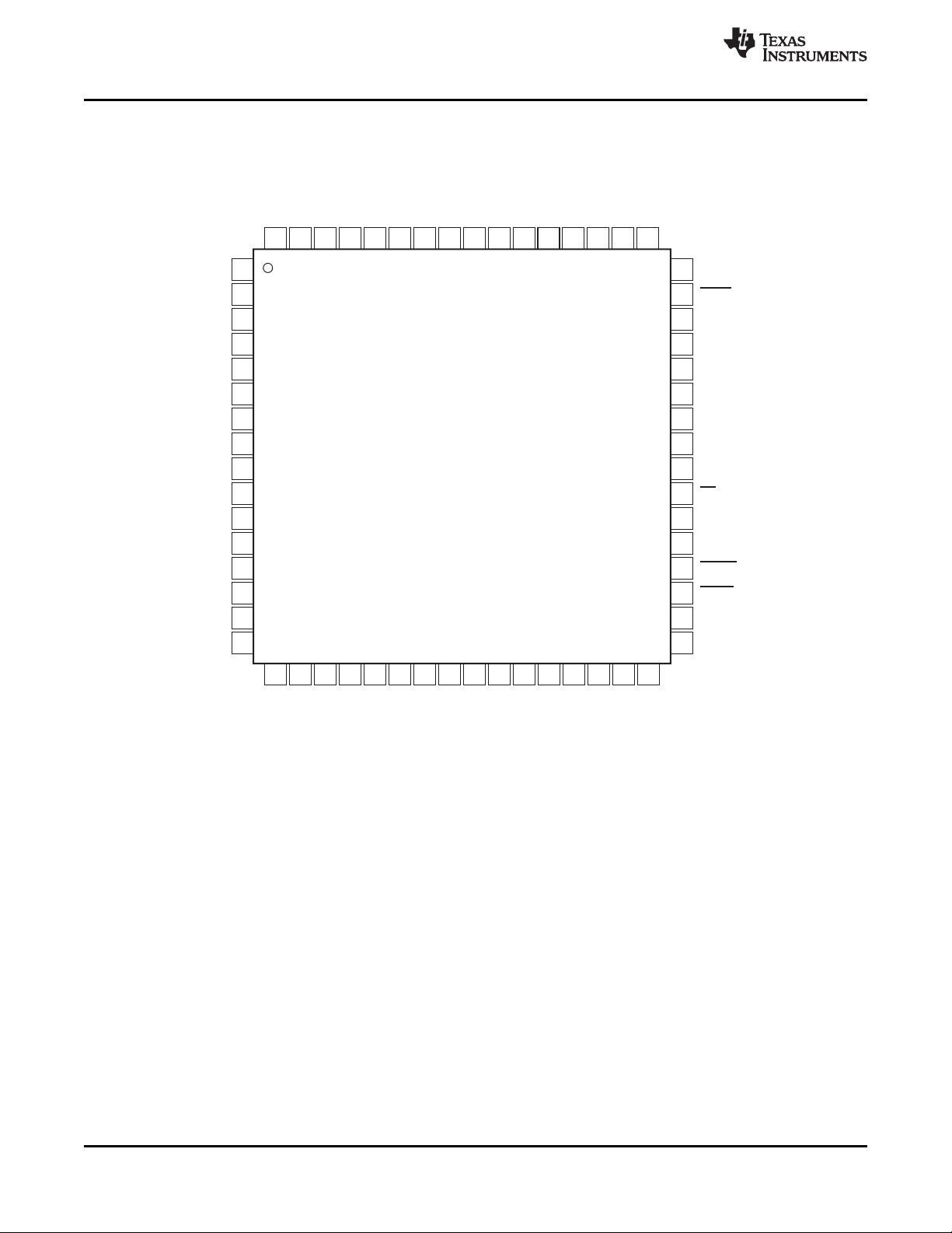
48
47
46
45
44
43
42
41
40
39
38
37
36
35
34
33
DVDD
GPIO4
GPIO3
GPIO2
DOUT
GPIO1
DAISY_IN
SCLK
START
CLK
DIN
DGND
DRDY
CS
RESET
PWDN
1
2
3
4
5
6
7
8
9
10
11
12
13
14
15
16
IN8N
IN8P
IN7N
IN7P
IN6N
IN6P
IN5N
IN5P
IN4N
IN4P
IN3N
IN3P
IN2N
IN2P
IN1N
IN1P
WCT
RLDOUT
RLDIN
RLDINV
RLDREF
AVDD
AVSS
AVSS
AVDD
VCAP3
AVDD1
AVSS1
CLKSEL
DGND
DVDD
DGND
TESTP_PACE_OUT1
TESTN_PACE_OUT2
AVDD
AVSS
AVDD
AVDD
AVSS
VREFP
VREFN
VCAP4
NC
VCAP1
NC
VCAP2
RESV1
AVSS
17
18
19
20
21
22
23
24
25
26
27
28
29
30
31
32
64
63
62
61
60
59
58
57
56
55
54
53
52
51
50
49
ADS1294, ADS1294R
ADS1296, ADS1296R
ADS1298, ADS1298R
ZHCS313I –JANUARY 2010– REVISED JANUARY 2012
www.ti.com.cn
PAG PACKAGE
TQFP-64
(TOP VIEW)
12 Copyright © 2010–2012, Texas Instruments Incorporated
Page 13

www.ti.com.cn
ZHCS313I –JANUARY 2010– REVISED JANUARY 2012
PAG PIN ASSIGNMENTS
NAME PIN FUNCTION DESCRIPTION
(1)
IN8N
(1)
IN8P
(1)
IN7N
(1)
IN7P
(1)
IN6N
(1)
IN6P
(1)
IN5N
(1)
IN5P
(1)
IN4N
(1)
IN4P
(1)
IN3N
(1)
IN3P
(1)
IN2N
(1)
IN2P
(1)
IN1N
(1)
IN1P
TESTP_PACE_OUT1
TESTN_PACE_OUT2
(1)
(1)
AVDD 19 Supply Analog supply
AVSS 20 Supply Analog ground
AVDD 21 Supply Analog supply
AVDD 22 Supply Analog supply
AVSS 23 Supply Analog ground
VREFP 24 Analog input/output Positive reference voltage
VREFN 25 Analog input Negative reference voltage
VCAP4 26 Analog output Analog bypass capacitor
NC 27 — No connection
VCAP1 28 — Analog bypass capacitor
NC 29 — No connection
VCAP2 30 — Analog bypass capacitor
RESV1 31 Digital input Reserved for future use; must tie to logic low (DGND).
AVSS 32 Supply Analog ground
DGND 33 Supply Digital ground
DIN 34 Digital input SPI data in
PWDN 35 Digital input Power-down; active low
RESET 36 Digital input System reset; active low
CLK 37 Digital input/output External Master clock input or internal clock output.
START 38 Digital input Start conversion
CS 39 Digital input SPI chip select; active low
SCLK 40 Digital input SPI clock
DAISY_IN 41 Digital input Daisy-chain input; if not used, short to DGND.
GPIO1 42 Digital input/output General-purpose input/output pin
DOUT 43 Digital output SPI data out
GPIO2 44 Digital input/output General-purpose input/output pin
GPIO3 45 Digital input/output General-purpose input/output pin
GPIO4 46 Digital input/output General-purpose input/output pin
DRDY 47 Digital output Data ready; active low
DVDD 48 Supply Digital power supply
DGND 49 Supply Digital ground
DVDD 50 Supply Digital power supply
1 Analog input Differential analog negative input 8 (ADS1298)
2 Analog input Differential analog positive input 8 (ADS1298)
3 Analog input Differential analog negative input 7 (ADS1298)
4 Analog input Differential analog positive input 7 (ADS1298)
5 Analog input Differential analog negative input 6 (ADS1296/8)
6 Analog input Differential analog positive input 6 (ADS1296/8)
7 Analog input Differential analog negative input 5 (ADS1296/8)
8 Analog input Differential analog positive input 5 (ADS1296/8)
9 Analog input Differential analog negative input 4
10 Analog input Differential analog positive input 4
11 Analog input Differential analog negative input 3
12 Analog input Differential analog positive input 3
13 Analog input Differential analog negative input 2
14 Analog input Differential analog positive input 2
15 Analog input Differential analog negative input 1
16 Analog input Differential analog positive input 1
17 Analog input/buffer output Internal test signal/single-ended buffer output based on register settings
18 Analog input/output Internal test signal/single-ended buffer output based on register settings
ADS1294, ADS1294R
ADS1296, ADS1296R
ADS1298, ADS1298R
(1) Connect unused terminals to AVDD.
Copyright © 2010–2012, Texas Instruments Incorporated 13
Page 14
ADS1294, ADS1294R
ADS1296, ADS1296R
ADS1298, ADS1298R
ZHCS313I –JANUARY 2010– REVISED JANUARY 2012
PAG PIN ASSIGNMENTS (continued)
NAME PIN FUNCTION DESCRIPTION
DGND 51 Supply Digital ground
CLKSEL 52 Digital input Master clock select
AVSS1 53 Supply Analog ground
AVDD1 54 Supply Analog supply
VCAP3 55 Analog Analog bypass capacitor; internally generated AVDD + 1.9V.
AVDD 56 Supply Analog supply
AVSS 57 Supply Analog ground
AVSS 58 Supply Analog ground
AVDD 59 Supply Analog supply
RLDREF 60 Analog input Right leg drive noninverting input
RLDINV 61 Analog input/output Right leg drive inverting input
(1)
RLDIN
RLDOUT 63 Analog output Right leg drive output
WCT 64 Analog output Wilson Central Terminal output
62 Analog input Right leg drive input to MUX
www.ti.com.cn
14 Copyright © 2010–2012, Texas Instruments Incorporated
Page 15
1
CS
SCLK
DIN
DOUT
2
3 8
1 2
83
t
CSSC
t
DIST
t
DIHD
t
DOHD
t
CSH
t
DOPD
t
SPWH
t
SPWL
t
SCCS
Hi-Z
t
CSDOZ
t
CSDOD
Hi-Z
t
SCLK
t
SDECODE
CLK
t
CLK
D ISY_INA
DOUT
SCLK
MSB
D1
t
DISCK2ST
MSB
21
3 216
217
218
MSB
D1
LSB
t
DISCK2HT
t
DOPD
Don’tCare
LSB
D1
219
www.ti.com.cn
TIMING CHARACTERISTICS
NOTE: SPI settings are CPOL = 0 and CPHA = 1.
ADS1294, ADS1294R
ADS1296, ADS1296R
ADS1298, ADS1298R
ZHCS313I –JANUARY 2010– REVISED JANUARY 2012
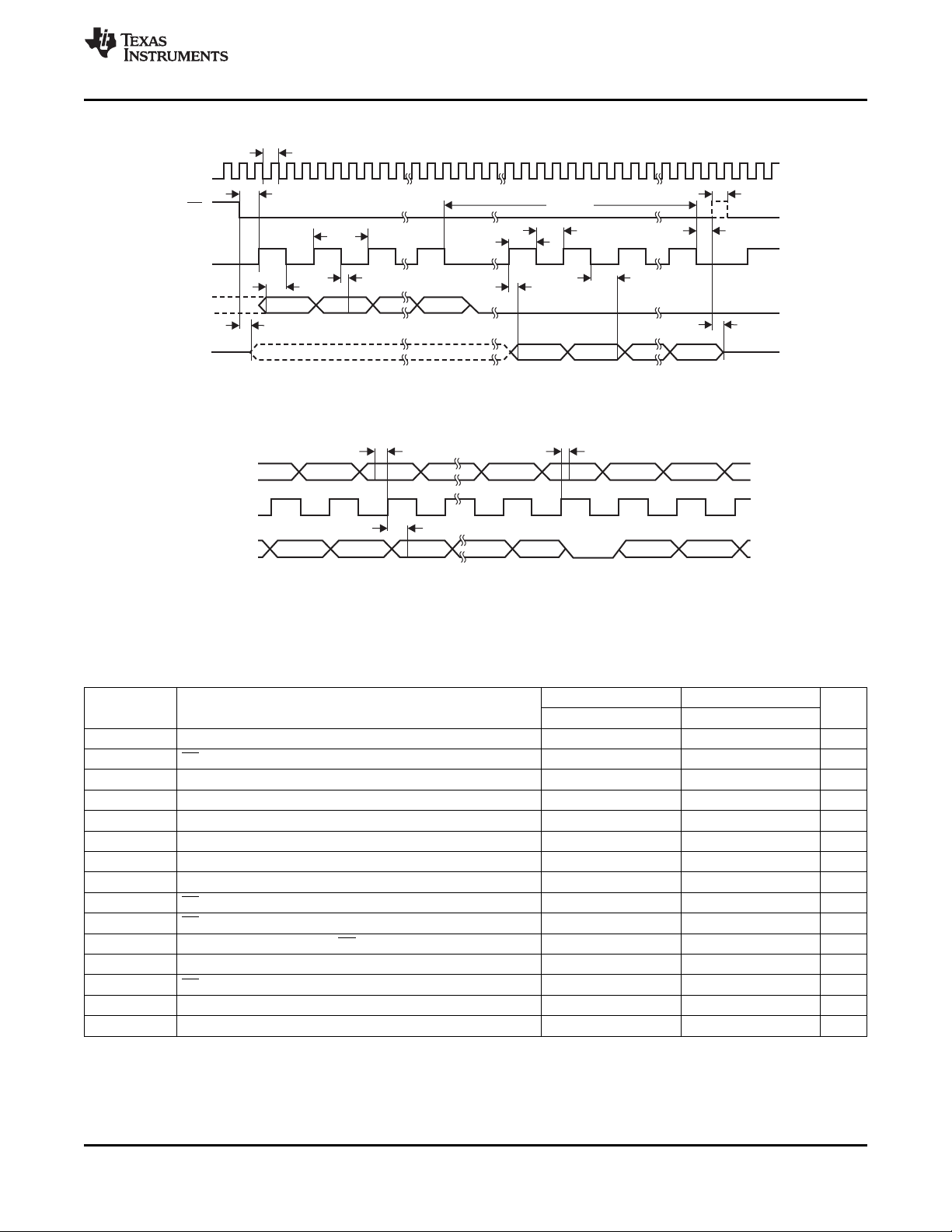
Figure 1. Serial Interface Timing
NOTE: Daisy-chain timing shown for eight-channel ADS1298, ADS1298R, and ADS1298I.
Figure 2. Daisy-Chain Interface Timing
Timing Requirements For Figure 1 and Figure 2
Specifications apply from –40°C to +85°C, unless otherwise noted. Load on D
PARAMETER DESCRIPTION MIN TYP MAX MIN TYP MAX UNIT
t
CLK
t
CSSC
t
SCLK
t
SPWH, L
t
DIST
t
DIHD
t
DOHD
t
DOPD
t
CSH
t
CSDOD
t
SCCS
t
SDECODE
t
CSDOZ
t
DISCK2ST
t
DISCK2HT
Copyright © 2010–2012, Texas Instruments Incorporated 15
Master clock period 414 514 414 514 ns
CS low to first SCLK, setup time 6 17 ns
SCLK period 50 66.6 ns
SCLK pulse width, high and low 15 25 ns
DIN valid to SCLK falling edge: setup time 10 10 ns
Valid DIN after SCLK falling edge: hold time 10 11 ns
SCLK falling edge to invalid DOUT: hold time 10 10 ns
SCLK rising edge to DOUT valid: setup time 17 32 ns
CS high pulse 2 2 t
CS low to DOUT driven 10 20 ns
Eighth SCLK falling edge to CS high 4 4 t
Command decode time 4 4 t
CS high to DOUT Hi-Z 10 20 ns
DAISY_IN valid to SCLK rising edge: setup time 10 10 ns
DAISY_IN valid after SCLK rising edge: hold time 10 10 ns
= 20pF || 100kΩ.
OUT
2.7V ≤ DVDD ≤ 3.6V 1.65V ≤ DVDD ≤ 2V
CLKs
CLKs
CLKs
Page 16
3
2
1
0
1
2
3
-
-
-
Time(sec)
Input-ReferredNoise( V)m
1 20 103 4 5 6 7 8 9
Peak-to-PeakOver10sec=5 Vm
1600
1400
1200
1000
800
600
400
200
0
Input-ReferredNoise( V)m
Occurrences
-2.88
-2.35
-1.85
-1.35
-0.84
-0.34
0.17
1.17
2.18
0.67
1.68
2.408
2.406
2.404
2.402
2.4
2.398
2.396
-40
85
Temperature( C)°
InternalReference(V)
-15 10
6035
-130
125
120
115
110
105
100
95
90
85
-
-
-
-
-
-
-
-
-
10
1k
Frequency(Hz)
Common-ModeRejectionRatio(dB)
100
Gain=1
DataRate=4kSPS
AIN=AVDD 0.3VtoAVSS+0.3V-
Gain=2
Gain=3
Gain=4
Gain=6
Gain=8
Gain=12
0.18
0.16
0.14
0.12
0.10
0.08
0.06
0.04
0.02
0
0.3
4.8
InputVoltage(V)
InputLeakageCurrent(nA)
2.3
AVDD AVSS=5V
PGA=1
-
1.81.30.8 2.8 3.3 3.8 4.3
1200
1000
800
600
400
200
0
-40
85
Temperature( C)°
LeakageCurrent(pA)
3510-15 60
ADS1294, ADS1294R
ADS1296, ADS1296R
ADS1298, ADS1298R
ZHCS313I –JANUARY 2010– REVISED JANUARY 2012
TYPICAL CHARACTERISTICS
All plots at TA= +25°C, AVDD = 3V, AVSS = 0V, DVDD = 1.8V, internal VREFP = 2.4V, VREFN = AVSS, external clock =
2.048MHz, data rate = 500SPS, High-Resolution mode, and gain = 6, unless otherwise noted.
INPUT-REFERRED NOISE NOISE HISTOGRAM
Figure 3. Figure 4.
www.ti.com.cn
INTERNAL REFERENCE vs TEMPERATURE CMRR vs FREQUENCY
Figure 5. Figure 6.
LEAKAGE CURRENT vs INPUT VOLTAGE LEAKAGE CURRENT vs TEMPERATURE
16 Copyright © 2010–2012, Texas Instruments Incorporated
Figure 7. Figure 8.
Page 17
110
105
100
95
90
85
80
75
70
10
1k
Frequency(Hz)
Power-SupplyRejectionRatio(dB)
100
DataRate=4kSPS
Gain=2
Gain=4
Gain=1
Gain=12
Gain=3
Gain=8
Gain=6
-105
100
95
90
85
80
75
70
-
-
-
-
-
-
-
10
1k
Frequency(Hz)
TotalHarmonicDistortion(dB)
100
DataRate=4kSPS
AIN=0.5dBFS
Gain=1
Gain=2
Gain=4
Gain=12
Gain=3
Gain=8
Gain=6
8
6
4
2
0
2
4
6
8
-
-
-
-
-1
1
InputRange(NormalizedtoFull-Scale)
IntegralNonlinearity(ppm)
-0.5
0.50
-40 C°
-20 C°
0 C°
+25 C°
+40 C°
+60 C°
+70 C°
+85 C°
10
8
6
4
2
0
2
4
6
8
10
-
-
-
-
-
Input(NormalizedtoFull-Scale)
IntegralNonlinearity(ppm)
-0.8-1.0 1.0-0.2 0.2 0.6-0.6 0.8-0.4 0 0.4
Gain=6
Gain=8
Gain=12
Gain=1
Gain=2
Gain=3
Gain=4
0
20
40
60
80
100
120
140
160
180
-
-
-
-
-
-
-
-
-
Frequency(Hz)
Amplitude(dBFS)
500 250100 150 200
PGAGain=1
THD= 102dB
SNR=115dB
f =500SPS
f =ExternalClock
-
DR
CLK
0
20
40
60
80
100
120
140
160
180
-
-
-
-
-
-
-
-
-
Frequency(kHz)
Amplitude(dBFS)
20 164 6 8
PGAGain=6
THD= 104dB
SNR=74.5dB
-
f =32kSPS
DR
10 12 14
ADS1294, ADS1294R
ADS1296, ADS1296R
ADS1298, ADS1298R
www.ti.com.cn
TYPICAL CHARACTERISTICS (continued)
All plots at TA= +25°C, AVDD = 3V, AVSS = 0V, DVDD = 1.8V, internal VREFP = 2.4V, VREFN = AVSS, external clock =
2.048MHz, data rate = 500SPS, High-Resolution mode, and gain = 6, unless otherwise noted.
PSRR vs FREQUENCY THD vs FREQUENCY
Figure 9. Figure 10.
ZHCS313I –JANUARY 2010– REVISED JANUARY 2012
INL vs PGA GAIN INL vs TEMPERATURE
Figure 11. Figure 12.
THD FFT PLOT FFT PLOT
(60Hz Signal) (60Hz Signal)
Copyright © 2010–2012, Texas Instruments Incorporated 17
Figure 13. Figure 14.
Page 18
800
700
600
500
400
300
200
100
0
1
12
PGAGain
Offset( V)m
8642 109753 11
70
60
50
40
30
20
10
0
-0.53
Error(%)
NumberofBins
-0.41
-0.18
0.06
0.30
0.54
0.66
0.42
0.18
-0.06
-0.29
DataFrom31Devices,TwoLots
80
70
60
50
40
30
20
10
0
-20
ThresholdError(mV)
NumberofBins
-15
0
10
20
30
35
25
15
5
-10
DataFrom31Devices,TwoLots
120
100
80
60
40
20
0
-2.70
ErrorinCurrentMagnitude(nA)
NumberofBins
-2.14
-1.01
0.12
1.24
2.37
2.93
1.80
0.68
-0.45
-1.57
DataFrom31Devices,TwoLots
CurrentSetting=24nA
17.5
15.5
13.5
11.5
9.5
7.5
5.5
3.5
1.5
Number of Channels Disabled
Power (mW)
10 84 62 3 5 7
AVDD = 3V
AVDD = 5V
40
30
20
10
0
10
20
30
40
50
-
-
-
-
-
InputRange(NormalizedtoFull-Scale)
IntegralNonlinearity(ppm)
-0.8-1 1-0.2 0.2-0.6 -0.4 0 0.4 0.80.6
Channel1
Channel2
Channel3
Channel4
Channel5
Channel6
Channel7
Channel8
ADS1294, ADS1294R
ADS1296, ADS1296R
ADS1298, ADS1298R
ZHCS313I –JANUARY 2010– REVISED JANUARY 2012
TYPICAL CHARACTERISTICS (continued)
All plots at TA= +25°C, AVDD = 3V, AVSS = 0V, DVDD = 1.8V, internal VREFP = 2.4V, VREFN = AVSS, external clock =
2.048MHz, data rate = 500SPS, High-Resolution mode, and gain = 6, unless otherwise noted.
OFFSET vs PGA GAIN
(ABSOLUTE VALUE) TEST SIGNAL AMPLITUDE ACCURACY
Figure 15. Figure 16.
www.ti.com.cn
LEAD-OFF COMPARATOR THRESHOLD ACCURACY DISTRIBUTION
LEAD-OFF CURRENT SOURCE ACCURACY
Figure 17. Figure 18.
ADS1294R/6R/8R NONLINEARITY ADS1298/8R CHANNEL POWER
18 Copyright © 2010–2012, Texas Instruments Incorporated
Figure 19. Figure 20.
Page 19
110
105
100
95
90
85
80
75
70
65
60
Channel
TotalHarmonicDistortion(dBc)
1 84 62 3 5 7
f =10Hz, 0.5dBFS-
IN
120
110
100
90
80
70
60
50
InputAmplitude(dBFS)
Signal-to-NoiseRatio(dB)
-50
-60 -0.5-20 -5-40 -30 -12 -2
InternalMasterClock,AVDD=3V
ExternalMasterClock,AVDD=3V
ExternalMasterClock,AVDD=5V
InternalMasterClock,AVDD=5V
ADS1294, ADS1294R
ADS1296, ADS1296R
ADS1298, ADS1298R
www.ti.com.cn
TYPICAL CHARACTERISTICS (continued)
All plots at TA= +25°C, AVDD = 3V, AVSS = 0V, DVDD = 1.8V, internal VREFP = 2.4V, VREFN = AVSS, external clock =
2.048MHz, data rate = 500SPS, High-Resolution mode, and gain = 6, unless otherwise noted.
ADS129xR THD (10Hz Sine Wave)
Figure 21. Figure 22.
ZHCS313I –JANUARY 2010– REVISED JANUARY 2012
SNR vs INPUT AMPLITUDE
Copyright © 2010–2012, Texas Instruments Incorporated 19
Page 20

ADS1294, ADS1294R
ADS1296, ADS1296R
ADS1298, ADS1298R
ZHCS313I –JANUARY 2010– REVISED JANUARY 2012
OVERVIEW
NOTE
The ADS1294R/6R/8R channel performance differs from the ADS1294/6/8 in regards to
respiration circuitry found on channel one. Unless otherwise noted, ADS129x refers to all
specifications and functional descriptions of the ADS1294, ADS1296, ADS1298,
ADS1294R, ADS1296R, and ADS1298R.
The ADS129x are low-power, multichannel, simultaneously-sampling, 24-bit delta-sigma (ΔΣ) analog-to-digital
converters (ADCs) with integrated programmable gain amplifiers (PGAs). These devices integrate various
ECG-specific functions that make them well-suited for scalable electrocardiogram (ECG),
electroencephalography (EEG), and electromyography (EMG) applications. The devices can also be used in
high-performance, multichannel data acquisition systems by powering down the ECG-specific circuitry.
The ADS129x have a highly programmable multiplexer that allows for temperature, supply, input short, and RLD
measurements. Additionally, the multiplexer allows any of the input electrodes to be programmed as the patient
reference drive. The PGA gain can be chosen from one of seven settings (1, 2, 3, 4, 6, 8, and 12). The ADCs in
the device offer data rates from 250SPS to 32kSPS. Communication to the device is accomplished using an
SPI-compatible interface. The device provides four GPIO pins for general use. Multiple devices can be
synchronized using the START pin.
The internal reference can be programmed to either 2.4V or 4V. The internal oscillator generates a 2.048MHz
clock. The versatile right leg drive (RLD) block allows the user to choose the average of any combination of
electrodes to generate the patient drive signal. Lead-off detection can be accomplished either by using a
pull-up/pull-down resistor or a current source/sink. An internal ac lead-off detection feature is also available. The
device supports both hardware PACE detection and software PACE detection. The Wilson Central Terminal
(WCT) block can be used to generate the WCT point of the standard 12-lead ECG.
Additionally, the ADS1294R, ADS1296R, and ADS1298R provide options for an internal respiration modulator
and a demodulator circuit in the signal path of channel 1.
www.ti.com.cn
20 Copyright © 2010–2012, Texas Instruments Incorporated
Page 21
DRDY
CLK
CLKSEL
START
MUX
Oscillator
Power-Supply Signal
SPI
DVDD
DGND
RLD
INV
RLD
OUT
RLD
REF
Lead-Off Excitation Source
PACE
OUT2
GPIO1
GPIO4/RCLKO
GPIO3/RCLKO
RESP
CLK
PACE
OUT1
CS
SCLK
DIN
DOUT
RLD
IN
ADS1298/8R
ADS1296/6R/8/8R
GPIO2
AVDD
AVSS
IN8P
IN8N
IN7P
IN7N
IN6P
IN6N
IN5P
IN5N
IN4P
IN4N
IN3P
IN3N
IN2P
IN2N
IN1P
IN1N
PGA1
DS
ADC1
PGA2
PGA3
PGA4
PGA5
PGA6
PGA7
PGA8
EMI
Filter
EMI
Filter
EMI
Filter
EMI
Filter
EMI
Filter
EMI
Filter
EMI
Filter
EMI
Filter
Temperature Sensor Input
RLD
Amplifier
PACE
Amplifier 2
PACE
Amplifier 1
WCT
B
C
A
From
Wmuxc
From
Wmuxa
From
Wmuxb
WCT
Reference
VREFP
VREFN
Control
PWDN
RESET
DS
ADC2
DS
ADC3
DS
ADC4
DS
ADC5
DS
ADC6
DS
ADC7
DS
ADC8
AVDD1
AVSS1
Test Signal
Internal Respiration
Modulator
( )ADS129xR
RESP
DEMOD
RESP_DEMOD_EN
ADS129xR
ADS129xR
RESP_MODP
RESP_MODN
G = 0.4
G = 0.4
www.ti.com.cn
ADS1294, ADS1294R
ADS1296, ADS1296R
ADS1298, ADS1298R
ZHCS313I –JANUARY 2010– REVISED JANUARY 2012
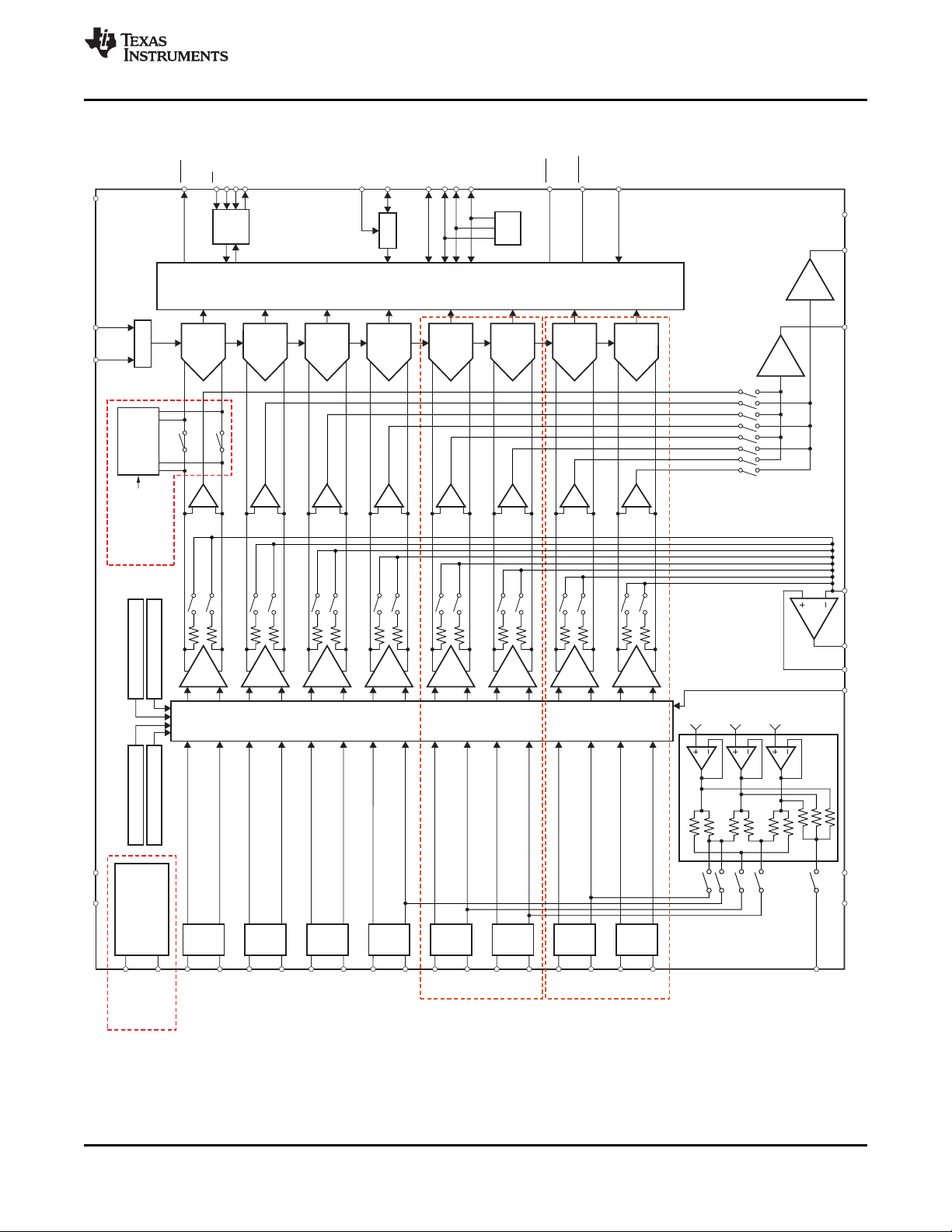
Figure 23. Functional Block Diagram
Copyright © 2010–2012, Texas Instruments Incorporated 21
Page 22
MUX[2:0]=101
TempP
MUX[2:0]= 100
MvddP
(1)
MUX[2:0]= 011
FromLoffP
MUX[2:0]= 000
MUX[2:0]= 110
MUX[2:0]= 001
ToPgaP
ToPgaN
MUX[2:0]= 001
RLDIN
MUX[2:0]= 010
RLD_MEAS
AND
MUX[2:0]= 111
VINP
VINN
MUX[2:0]= 000
FromLoffN
RLD_REF
MUX[2:0]= 010
RLD_MEAS
AND
MvddN
(1)
TempN
MUX[2:0]= 100
MUX[2:0]= 101
ADS129x
MUX
TestP
TestN
TESTP_PACE_OUT1
INT_TEST
INT_TEST
TESTN_PACE_OUT2
INT_TEST
INT_TEST
MUX[2:0]= 011
EMI
Filter
(AVDD+AVSS)
2
ADS1294, ADS1294R
ADS1296, ADS1296R
ADS1298, ADS1298R
ZHCS313I –JANUARY 2010– REVISED JANUARY 2012
THEORY OF OPERATION
This section discusses the details of the ADS129x internal functional elements. The analog blocks are reviewed
first, followed by the digital interface. Blocks implementing ECG-specific functions are covered in the end.
Throughout this document, f
denotes the frequency of the signal at the CLK pin, t
CLK
denotes the period of the
CLK
signal at the CLK pin, fDRdenotes the output data rate, tDRdenotes the time period of the output data, and f
denotes the frequency at which the modulator samples the input.
EMI FILTER
An RC filter at the input acts as an EMI filter on all of the channels. The –3dB filter bandwidth is approximately
3MHz.
INPUT MULTIPLEXER
The ADS129x input multiplexers are very flexible and provide many configurable signal switching options.
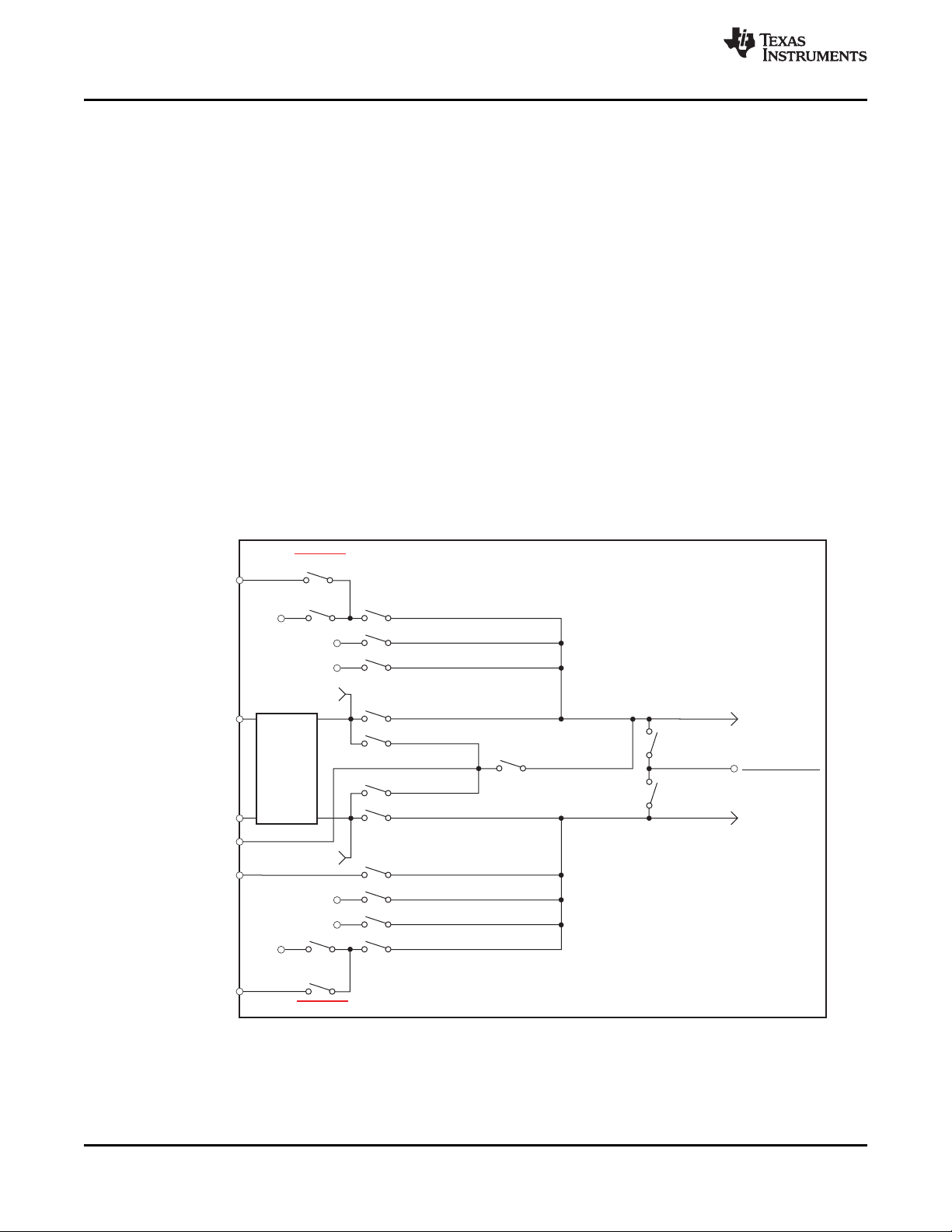
Figure 24 shows the multiplexer on a single channel of the device. Note that the device has eight such blocks,
one for each channel. TEST_PACE_OUT1, TEST_PACE_OUT2, and RLD_IN are common to all eight blocks.
VINP and VINN are separate for each of the eight blocks. This flexibility allows for significant device and
sub-system diagnostics, calibration, and configuration. Selection of switch settings for each channel is made by
writing the appropriate values to the CHnSET[2:0] register (see the CHnSET: Individual Channel Settings section
for details) and by writing the RLD_MEAS bit in the CONFIG3 register (see the CONFIG3: Configuration Register
3 subsection of the Register Map section for details). More details of the ECG-specific features of the multiplexer
are presented in the Input Multiplexer subsection of the ECG-Specifc Functions section.
www.ti.com.cn
MOD
22 Copyright © 2010–2012, Texas Instruments Incorporated
(1) MVDD monitor voltage supply depends on channel number; see the Supply Measurements (MVDDP, MVDDN)
section.
Figure 24. Input Multiplexer Block for One Channel
Page 23
Temperature( C)=°
TemperatureReading( V) 145,300 Vm - m
490 V/ Cm °
+25 C°
2x
1x
1x
8x
AVDD
AVSS
TemperatureSensorMonitor
ToMUXTempP
ToMUXTempN
ADS1294, ADS1294R
ADS1296, ADS1296R
ADS1298, ADS1298R
www.ti.com.cn
Device Noise Measurements
Setting CHnSET[2:0] = 001 sets the common-mode voltage of (AVDD – AVSS)/2 to both inputs of the channel.
This setting can be used to test the inherent noise of the device in the user system.
Test Signals (TestP and TestN)
Setting CHnSET[2:0] = 101 provides internally-generated test signals for use in sub-system verification at
power-up. This functionality allows the entire signal chain to be tested out. Although the test signals are similar to
the CAL signals described in the IEC60601-2-51 specification, this feature is not intended for use in compliance
testing.
Control of the test signals is accomplished through register settings (see the CONFIG2: Configuration Register 2
subsection in the Register Map section for details). TEST_AMP controls the signal amplitude and TEST_FREQ
controls switching at the required frequency.
The test signals are multiplexed and transmitted out of the device at the TESTP_PACE_OUT1 and
TESTN_PACE_OUT2 pins. A bit register (CONFIG2.INT_TEST = 0) deactivates the internal test signals so that
the test signal can be driven externally. This feature allows the calibration of multiple devices with the same
signal. The test signal feature cannot be used in conjunction with the external hardware PACE feature (see the
External Hardware Approach subsection of the ECG-Specific Functions section for details).
Auxiliary Differential Input (TESTP_PACE_OUT1, TESTN_PACE_OUT2)
When hardware PACE detect is not used, the TESTP_PACE_OUT1 and TESPN_PACE_OUT2 signals can be
used as a multiplexed differential input channel. These inputs can be multiplexed to any of the eight channels.
The performance of the differential input signal fed through these pins is identical to the normal channel
performance.
ZHCS313I –JANUARY 2010– REVISED JANUARY 2012
Temperature Sensor (TempP, TempN)
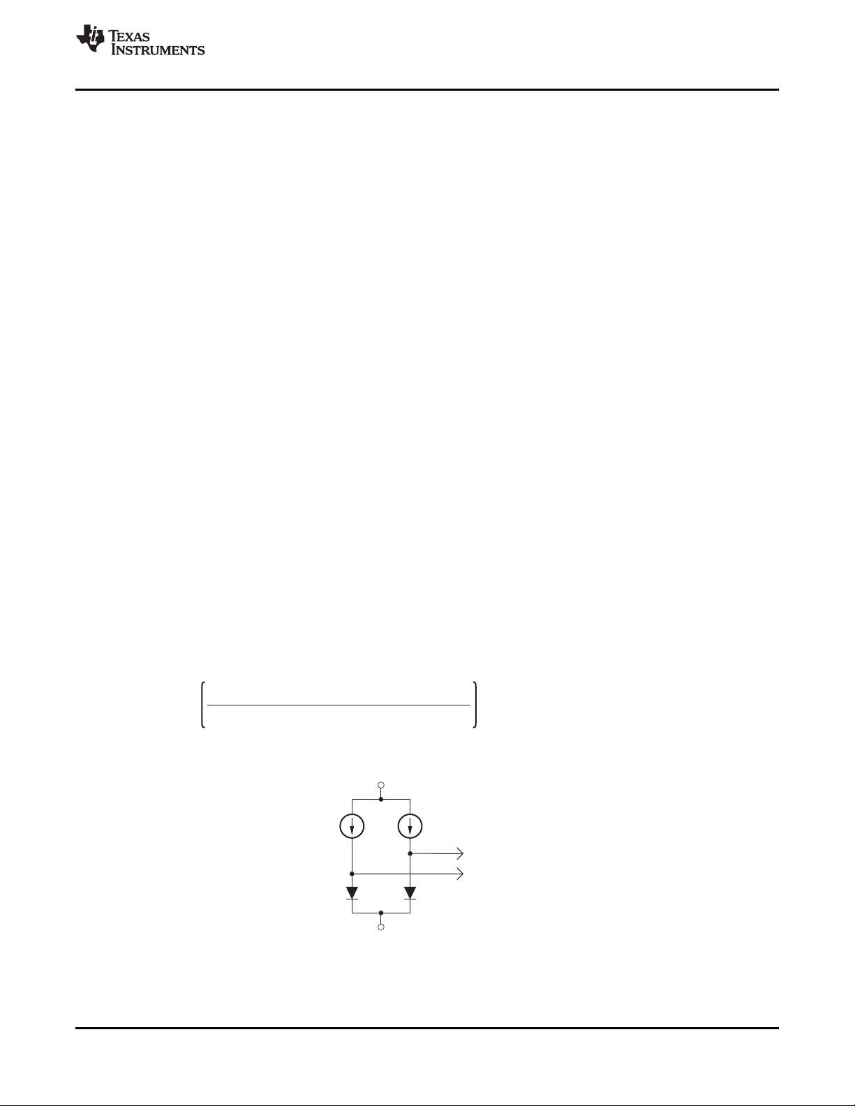
The ADS129x contain an on-chip temperature sensor. This sensor uses two internal diodes with one diode
having a current density 16x that of the other, as shown in Figure 25. The difference in current densities of the
diodes yields a difference in voltage that is proportional to absolute temperature.
As a result of the low thermal resistance of the package to the printed circuit board (PCB), the internal device
temperature tracks the PCB temperature closely. Note that self-heating of the ADS129x causes a higher reading
than the temperature of the surrounding PCB.
The scale factor of Equation 1 converts the temperature reading to °C. Before using this equation, the
temperature reading code must first be scaled to μV.
(1)
Copyright © 2010–2012, Texas Instruments Incorporated 23
Figure 25. Measurement of the Temperature Sensor in the Input
Page 24
ADS1298
- V to
+1/2V
REF
REF
1/2
Common
Voltage
Single-EndedInput
ADS1298
V
peak-to-peak
REF
V
peak-to-peak
REF
Common
Voltage
DifferentialInput
ADS1294, ADS1294R
ADS1296, ADS1296R
ADS1298, ADS1298R
ZHCS313I –JANUARY 2010– REVISED JANUARY 2012
Supply Measurements (MVDDP, MVDDN)
Setting CHnSET[2:0] = 011 sets the channel inputs to different supply voltages of the device. For channels 1, 2,
5, 6, 7, and 8, (MVDDP – MVDDN) is [0.5 × (AVDD – AVSS)]; for channel 3 and for channel 4, (MVDDP –
MVDDN) is DVDD/4. Note that to avoid saturating the PGA while measuring power supplies, the gain must be
set to '1'. For example, if AVDD = 2.5V and AVSS = –2.5V, then the measurement result would be 2.5V.
Lead-Off Excitation Signals (LoffP, LoffN)
The lead-off excitation signals are fed into the multiplexer before the switches. The comparators that detect the
lead-off condition are also connected to the multiplexer block before the switches. For a detailed description of
the lead-off block, refer to the Lead-Off Detection subsection in the ECG-Specific Functions section.
Auxiliary Single-Ended Input
The RLD_IN pin is primarily used for routing the right leg drive signal to any of the electrodes in case the right leg
drive electrode falls off. However, the RLD_IN pin can be used as a multiple single-ended input channel. The
signal at the RLD_IN pin can be measured with respect to the voltage at the RLD_REF pin using any of the eight
channels. This measurement is done by setting the channel multiplexer setting to '010' and the RLD_MEAS bit of
the CONFIG3 register to '1'.
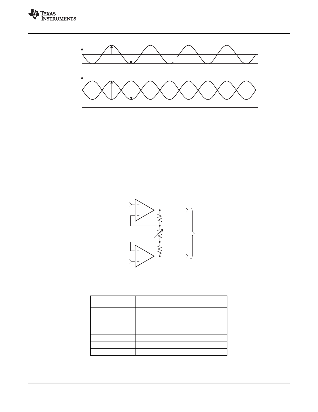
ANALOG INPUT
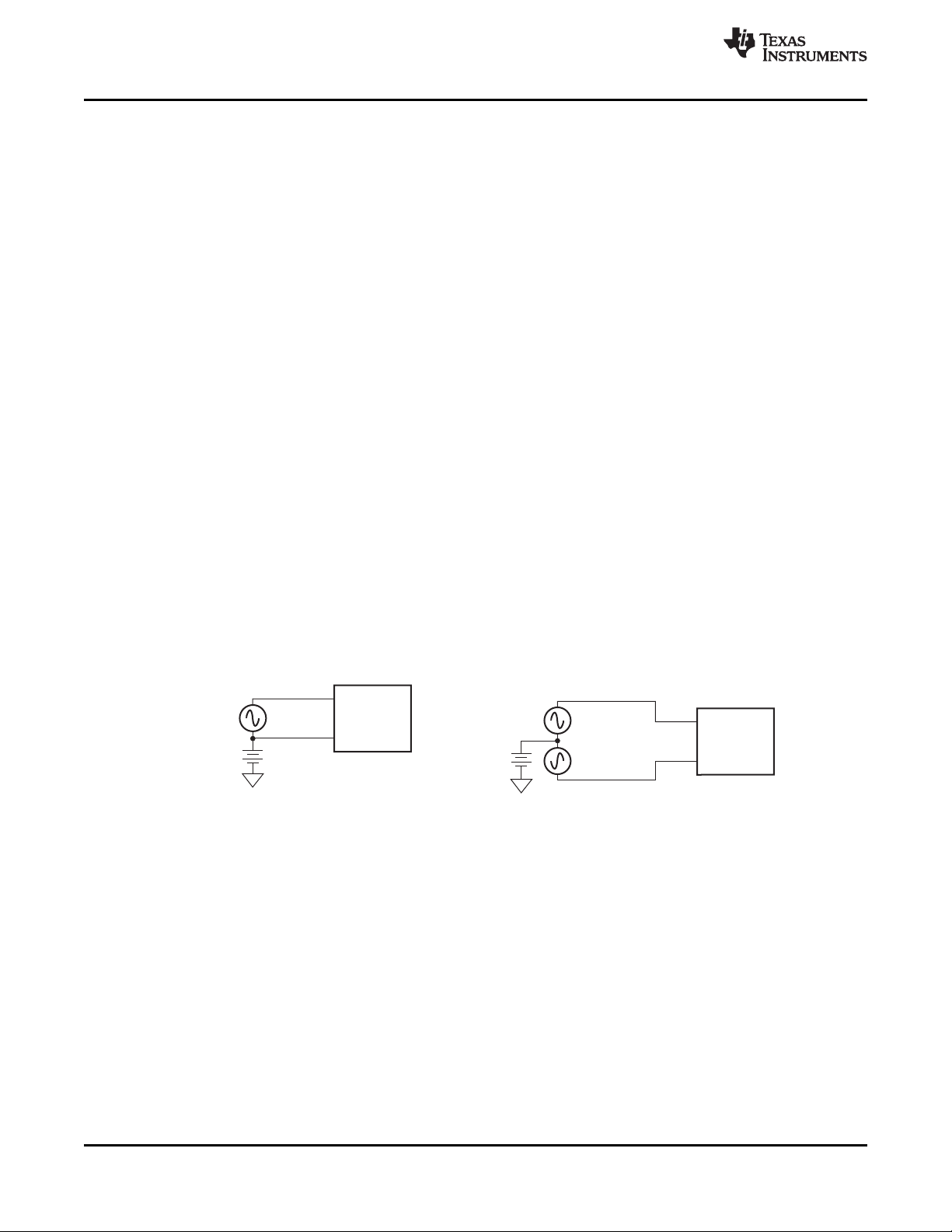
The analog input to the ADS1298 is fully differential. Assuming PGA = 1, the differential input (INP – INN) can
span between –V
and AVDD + 0.3V. Refer to Table 8 for an explanation of the correlation between the analog input and the digital
codes. There are two general methods of driving the analog input of the ADS1298: single-ended or differential,
as shown in Figure 26 and Figure 27. Note that INP and INN are 180°C out-of-phase in the differential input
method. When the input is single-ended, the INN input is held at the common-mode voltage, preferably at
mid-supply. The INP input swings around the same common voltage and the peak-to-peak amplitude is the
(common-mode + 1/2V
is given by (INP + INN)/2. Both the INP and INN inputs swing from (common-mode + 1/2V
common-mode – 1/2V
differential configuration.
REF
to +V
REF
REF
. Note that the the absolute range for INP and INN must be between AVSS – 0.3V
REF
) and the (common-mode – 1/2V
). When the input is differential, the common-mode
REF
). For optimal performance, it is recommended that the ADS1298 devices be used in a
www.ti.com.cn
REF
to
Figure 26. Methods of Driving the ADS1298: Single-Ended or Differential
24 Copyright © 2010–2012, Texas Instruments Incorporated
Page 25
CM+1/2V
REF
+1/2V
REF
- V
REF
1/2
Single-EndedInputs
t
INP
CMVoltage
CM V-
REF
1/2
CM+1/2V
REF
DifferentialInputs
t
INP
INN
CMVoltage
CM 1/2V
REF
-
+V
REF
-V
REF
Common-ModeVoltage(DifferentialMode)=
(INP)+(INN)
2
,Common-ModeVoltage(Single-EndedMode)= INN.
INN=CMVoltage
InputRange(DifferentialMode)=(AINP AINN)=V ( V )=2V .-
REF REF
- -
REF
PgaP
R
50kW
2
R
20k
(forGain=6)
W
1
R
50kW
2
FromMuxP
PgaN
FromMuxN
ToADC
ADS1294, ADS1294R
ADS1296, ADS1296R
ADS1298, ADS1298R
www.ti.com.cn
Figure 27. Using the ADS1298 in the Single-Ended and Differential Input Modes
PGA SETTINGS AND INPUT RANGE
The PGA is a differential input/differential output amplifier, as shown in Figure 28. It has seven gain settings (1,
2, 3, 4, 6, 8, and 12) that can be set by writing to the CHnSET register (see the CHnSET: Individual Channel
Settings subsection of the Register Map section for details). The ADS129x have CMOS inputs and hence have
negligible current noise. Table 6 shows the typical values of bandwidths for various gain settings. Note that
Table 6 shows the small-signal bandwidth. For large signals, the performance is limited by the slew rate of the
PGA.
ZHCS313I –JANUARY 2010– REVISED JANUARY 2012
Figure 28. PGA Implementation
Table 6. PGA Gain versus Small-Signal Bandwidth
GAIN TEMPERATURE (kHz)
1 237
2 146
Copyright © 2010–2012, Texas Instruments Incorporated 25
3 127
4 96
6 64
8 48
12 32
NOMINAL BANDWIDTH AT ROOM
Page 26
AVDD 0.2- -
GainV
MAX_DIFF
2
>CM>AVSS+0.2+
GainV
MAX_DIFF
2
Max(INP INN)<-
V
REF
Gain
Full-ScaleRange=
±V
REF
Gain
; =
2V
REF
Gain
−160
−150
−140
−130
−120
−110
−100
−90
−80
−70
−60
−50
−40
−30
−20
−10
0
0.001 0.01 0.1 1
Normalized Frequency (fIN/f
MOD
)
Power Spectral Density (dB)
G001
ADS1294, ADS1294R
ADS1296, ADS1296R
ADS1298, ADS1298R
ZHCS313I –JANUARY 2010– REVISED JANUARY 2012
The resistor string of the PGA that implements the gain has 120kΩ of resistance for a gain of 6. This resistance
provides a current path across the outputs of the PGA in the presence of a differential input signal. This current
is in addition to the quiescent current specified for the device in the presence of a differential signal at the input.
Input Common-Mode Range
The usable input common-mode range of the front end depends on various parameters, including the maximum
differential input signal, supply voltage, PGA gain, etc. This range is described in Equation 2:
where:
V
MAX_DIFF
= maximum differential signal at the input of the PGA
CM = common-mode range (2)
For example:
If VDD= 3V, gain = 6, and V
MAX_DIFF
= 350mV
Then 1.25V < CM < 1.75V
www.ti.com.cn
Input Differential Dynamic Range
The differential (INP – INN) signal range depends on the analog supply and reference used in the system. This
range is shown in Equation 3.
(3)
The 3V supply, with a reference of 2.4V and a gain of 6 for ECGs, is optimized for power with a differential input
signal of approximately 300mV. For higher dynamic range, a 5V supply with a reference of 4V (set by the
VREF_4V bit of the CONFIG3 register) can be used to increase the differential dynamic range.
ADC ΔΣ Modulator
Each channel of the ADS129x has a 24-bit ΔΣ ADC. This converter uses a second-order modulator optimized for
low-power applications. The modulator samples the input signal at the rate of f
mode and f
shaped until f
= f
MOD
MOD
/8 for Low-Power mode. As in the case of any ΔΣ modulator, the noise of the ADS129x is
CLK
/2, as shown in Figure 29. The on-chip digital decimation filters explained in the next section
MOD
= f
/4 for High-Resolution
CLK
can be used to filter out the noise at higher frequencies. These on-chip decimation filters also provide antialias
filtering. This feature of the ΔΣ converters drastically reduces the complexity of the analog antialiasing filters that
are typically needed with Nyquist ADCs.
26 Copyright © 2010–2012, Texas Instruments Incorporated
Figure 29. Modulator Noise Spectrum Up To 0.5 × f
MOD
Page 27

½H(z) =½
3
1 Z-
- N
1 Z-
- 1
3
sin
N fp
f
MOD
N sin´
pf
f
MOD
ADS1294, ADS1294R
ADS1296, ADS1296R
ADS1298, ADS1298R
www.ti.com.cn
DIGITAL DECIMATION FILTER
The digital filter receives the modulator output and decimates the data stream. By adjusting the amount of
filtering, tradeoffs can be made between resolution and data rate: filter more for higher resolution, filter less for
higher data rates. Higher data rates are typically used in ECG applications for implement software PACE
detection and ac lead-off detection.
The digital filter on each channel consists of a third-order sinc filter. The decimation ratio on the sinc filters can
be adjusted by the DR bits in the CONFIG1 register (see the Register Map section for details). This setting is a
global setting that affects all channels and, therefore, in a device all channels operate at the same data rate.
Sinc Filter Stage (sinx/x)
The sinc filter is a variable decimation rate, third-order, low-pass filter. Data are supplied to this section of the
filter from the modulator at the rate of f
then decimates the data stream into parallel data. The decimation rate affects the overall data rate of the
converter.
Equation 4 shows the scaled Z-domain transfer function of the sinc filter.
The frequency domain transfer function of the sinc filter is shown in Equation 5.
. The sinc filter attenuates the high-frequency noise of the modulator,
MOD
ZHCS313I –JANUARY 2010– REVISED JANUARY 2012
(4)
where:
N = decimation ratio (5)
Copyright © 2010–2012, Texas Instruments Incorporated 27
Page 28

0
-20
-40
-60
-80
-100
-120
-140
NormalizedFrequency(f /f )
IN DR
Gain(dB)
1.0 2.00 3.0 4.0 5.00.5 4.53.52.51.5
0
0.5
1.0
1.5
2.0
2.5
3.0
-
-
-
-
-
-
NormalizedFrequency(f /f )
IN DR
Gain(dB)
0.05 0.100 0.15 0.350.20 0.25 0.30
0
20
40
60
80
100
120
140
-
-
-
-
-
-
-
NormalizedFrequency(f /f )
IN MOD
Gain(dB)
0.05 0.100 0.500.15 0.20 0.25 0.30 0.35 0.40 0.45
DR[2:0]=110
DR[2:0]=000
0
20
40
60
80
100
120
140
-
-
-
-
-
-
-
NormalizedFrequency(f /f )
IN MOD
Gain(dB)
0.010 0.070.02 0.03 0.04 0.05 0.06
DR[2:0]=000
DR[2:0]=110
10
10
30
50
70
90
110
130
-
-
-
-
-
-
-
NormalizedFrequency(f /f )
IN MOD
Gain(dB)
0.50 4.01.0 1.5 2.0 2.5 3.0 3.5
DR[2:0]=110DR[2:0]=000
ADS1294, ADS1294R
ADS1296, ADS1296R
ADS1298, ADS1298R
ZHCS313I –JANUARY 2010– REVISED JANUARY 2012
The sinc filter has notches (or zeroes) that occur at the output data rate and multiples thereof. At these
frequencies, the filter has infinite attenuation. Figure 30 shows the frequency response of the sinc filter and
Figure 31 shows the roll-off of the sinc filter. With a step change at input, the filter takes 3 × tDRto settle. After a
rising edge of the START signal, the filter takes t
time to give the first data output. The settling time of the
SETTLE
filters at various data rates are discussed in the START subsection of the SPI Interface section. Figure 32 and
Figure 33 show the filter transfer function until f
shows the transfer function extended until 4 × f
itself at every f
in frequencies around multiples of f
. The input R-C anti-aliasing filters in the system should be chosen such that any interference
MOD
are attenuated sufficiently.
MOD
/2 and f
MOD
. It can be seen that the passband of the ADS129x repeats
MOD
/16, respectively, at different data rates. Figure 34
MOD
www.ti.com.cn
Figure 30. Sinc Filter Frequency Response Figure 31. Sinc Filter Roll-Off
Figure 32. Transfer Function of On-Chip Figure 33. Transfer Function of On-Chip
Decimation Filters Until f
/2 Decimation Filters Until f
MOD
MOD
/16
Figure 34. Transfer Function of On-Chip Decimation Filters
Until 4f
28 Copyright © 2010–2012, Texas Instruments Incorporated
for DR[2:0] = 000 and DR[2:0] = 110
MOD
Page 29

22 Fm
ToADCReferenceInputs
VCAP1
10 Fm
VREFP
VREFN
Bandgap
2.4Vor4V
AVSS
R1
(1)
R3
(1)
R2
(1)
100W
100kW
100W
OPA211
10pF
0.1 Fm
+5V
0.1 Fm10 Fm
100 Fm22 Fm
OUTVIN+5V
TRIM
22 Fm
REF5025
ToVREFPPin
ADS1294, ADS1294R
ADS1296, ADS1296R
ADS1298, ADS1298R
www.ti.com.cn
REFERENCE
Figure 35 shows a simplified block diagram of the internal reference of the ADS129x. The reference voltage is
generated with respect to AVSS. When using the internal voltage reference, connect VREFN to AVSS.
ZHCS313I –JANUARY 2010– REVISED JANUARY 2012
(1) For V
= 2.4V: R1 = 12.5kΩ, R2 = 25kΩ, and R3 = 25kΩ. For V
REF
= 4V: R1 = 10.5kΩ, R2 = 15kΩ, and R3 = 35kΩ.
REF
Figure 35. Internal Reference
The external band-limiting capacitors determine the amount of reference noise contribution. For high-end ECG
systems, the capacitor values should be chosen such that the bandwidth is limited to less than 10Hz, so that the
reference noise does not dominate the system noise. When using a 3V analog supply, the internal reference
must be set to 2.4V. In case of a 5V analog supply, the internal reference can be set to 4V by setting the
VREF_4V bit in the CONFIG2 register.
Alternatively, the internal reference buffer can be powered down and VREFP can be applied externally. Figure 36
shows a typical external reference drive circuitry. Power-down is controlled by the PD_REFBUF bit in the
CONFIG3 register. By default the device wakes up in external reference mode.
Copyright © 2010–2012, Texas Instruments Incorporated 29
Figure 36. External Reference Driver
Page 30

ADS1294, ADS1294R
ADS1296, ADS1296R
ADS1298, ADS1298R
ZHCS313I –JANUARY 2010– REVISED JANUARY 2012
CLOCK
The ADS129x provide two different methods for device clocking: internal and external. Internal clocking is ideally
suited for low-power, battery-powered systems. The internal oscillator is trimmed for accuracy at room
temperature. Over the specified temperature range the accuracy varies; see the Electrical Characteristics. Clock
selection is controlled by the CLKSEL pin and the CLK_EN register bit.
The CLKSEL pin selects either the internal or external clock. The CLK_EN bit in the CONFIG1 register enables
and disables the oscillator clock to be output in the CLK pin. A truth table for these two pins is shown in Table 7.
The CLK_EN bit is useful when multiple devices are used in a daisy-chain configuration. It is recommended that
during power-down the external clock be shut down to save power.
Table 7. CLKSEL Pin and CLK_EN Bit
CLKSEL PIN BIT CLOCK SOURCE CLK PIN STATUS
0 X External clock Input: external clock
1 0 Internal clock oscillator 3-state
1 1 Internal clock oscillator Output: internal clock oscillator
CONFIG1.CLK_EN
DATA FORMAT
The ADS129x output 24 bits of data per channel in binary twos complement format, MSB first. The LSB has a
weight of V
full-scale input produces an output code of 800000h. The output clips at these codes for signals exceeding
full-scale. Table 8 summarizes the ideal output codes for different input signals. Note that for DR[2:0] = 000 and
001, the device has only 17 and 19 bits of resolution, respectively. The last seven (in 17-bit mode) or five (in
19-bit mode) bits can be ignored.
/(223– 1). A positive full-scale input produces an output code of 7FFFFFh and the negative
REF
www.ti.com.cn
Table 8. Ideal Output Code versus Input Signal
INPUT SIGNAL, V
(AINP – AINN) IDEAL OUTPUT CODE
≥ V
REF
+V
/(223– 1) 000001h
REF
0 000000h
–V
/(223– 1) FFFFFFh
REF
≤ –V
(1) Only valid for 24-bit resolution data rates.
(2) Assumes gain = 1.
(3) Excludes effects of noise, linearity, offset, and gain error.
(223/223– 1) 800000h
REF
IN
7FFFFFh
(1)(2)
(3)
30 Copyright © 2010–2012, Texas Instruments Incorporated
Page 31

ADS1294, ADS1294R
ADS1296, ADS1296R
ADS1298, ADS1298R
www.ti.com.cn
SPI INTERFACE
The SPI-compatible serial interface consists of four signals: CS, SCLK, DIN, and DOUT. The interface reads
conversion data, reads and writes registers, and controls the ADS129x operation. The DRDY output is used as a
status signal to indicate when data are ready. DRDY goes low when new data are available.
Chip Select (CS)
Chip select (CS) selects the ADS129x devices for SPI communication. While CS is low the serial interface is
active CS must remain low for the entire duration of the serial communication. After the serial communication is
finished, always wait four or more t
is reset, SCLK and DIN are ignored, and DOUT enters a high-impedance state. DRDY asserts when data
conversion is complete, regardless of whether CS is high or low.
While ADS129x is selected the device will attempt to decode and execute commands every eight serial clocks. If
the devices ceases to execute serial commands, it is possible extra clock pulses were presented and placed the
serial interface in an unknown state. Take CS high and back low to reset the serial interface to a known state.
Serial Clock (SCLK)
SCLK is the serial peripheral interface (SPI) serial clock. It is used to shift in commands and shift out data from
the device. The serial clock (SCLK) features a Schmitt-triggered input and clocks data on the DIN and DOUT
pins into and out of the ADS129x. Even though the input has hysteresis, it is recommended to keep SCLK as
clean as possible to prevent glitches from accidentally forcing a clock event. The absolute maximum limit for
SCLK is specified in the Serial Interface Timing table.
While ADS129x is selected(CS = LOW), the device attempts to decode and execute commands every eight
serial clocks. It is therefore recommended that multiples of 8 SCLKs be presented every serial transfer to keep
the interface in a normal operating mode. If the interface ceases to function because of extra serial clocks, it can
be reset by toggling CS high and back to low.
cycles before taking CS high. When CS is taken high, the serial interface
CLK
ZHCS313I –JANUARY 2010– REVISED JANUARY 2012
For a single device, the minimum speed needed for the SCLK depends on the number of channels, number of
bits of resolution, and output data rate. (For multiple cascaded devices, see the Cascade Mode subsection of the
Multiple Device Configuration section.)
t
SCLK
< (tDR– 4t
CLK
)/(N
BITS
× N
CHANNELS
+ 24) (6)
For example, if the ADS1298 is used in a 500SPS mode (eight channels, 24-bit resolution), the minimum SCLK
speed is 110kHz.
Data retrieval can be done either by putting the device in RDATAC mode or by issuing a RDATA command for
data on demand. The above SCLK rate limitation applies to RDATAC. For the RDATA command, the limitation
applies if data must be read between two consecutive DRDY signals. The above calculation assumes that there
are no other commands issued between data captures.
Data Input (DIN)
The data input pin (DIN) is used along with SCLK to communicate with the ADS129x (opcode commands and
register data). The device latches data on DIN on the falling edge of SCLK.
Copyright © 2010–2012, Texas Instruments Incorporated 31
Page 32

CS
SCLK
DRDY
DOUT
STAT
24-Bit 24-Bit 24-Bit 24-Bit 24-Bit 24-Bit 24-Bit 24-Bit 24-Bit
CH1 CH2 CH3 CH4 CH5 CH6 CH7 CH8
216SCLKs
DIN
ADS1294, ADS1294R
ADS1296, ADS1296R
ADS1298, ADS1298R
ZHCS313I –JANUARY 2010– REVISED JANUARY 2012
Data Output (DOUT)
The data output pin (DOUT) is used with SCLK to read conversion and register data from the ADS129x. Data on
DOUT are shifted out on the rising edge of SCLK. DOUT goes to a high-impedance state when CS is high. In
read data continuous mode (see the SPI Command Definitions section for more details), the DOUT output line
also indicates when new data are available. This feature can be used to minimize the number of connections
between the device and the system controller.
Figure 37 shows the data output protocol for ADS1298.
Figure 37. SPI Bus Data Output for the ADS1298 (Eight Channels)
www.ti.com.cn
Data Retrieval
Data retrieval can be accomplished in one of two methods. The read data continuous command (see the
RDATAC: Read Data Continuous section) can be used to set the device in a mode to read the data continuously
without sending opcodes. The read data command (see the RDATA: Read Data section) can be used to read
just one data output from the device (see the SPI Command Definitions section for more details). The conversion
data are read by shifting the data out on DOUT. The MSB of the data on DOUT is clocked out on the first SCLK
rising edge. DRDY returns to high on the first SCLK falling edge. DIN should remain low for the entire read
operation.
The number of bits in the data output depends on the number of channels and the number of bits per channel.
For the ADS1298/8R, the number of data outputs is (24 status bits + 24 bits × 8 channels) = 216 bits. The format
of the 24 status bits is: (1100 + LOFF_STATP + LOFF_STATN + bits[4:7] of the GPIO register). The data format
for each channel data are twos complement and MSB first. When channels are powered down using the user
register setting, the corresponding channel output is set to '0'. However, the sequence of channel outputs
remains the same. For the ADS1294/4R and ADS1296/6R, the last four and two channel outputs shown in
Figure 37 are zeros. The four and six channels parts require only 120 and 168 SCLKs to shift data out,
respectively. Status and GPIO register bits are loaded into the 24-bit status word 2t
s before DRDY goes low.
CLK
The ADS129x also provide a multiple readback feature. The data can be read out multiple times by simply giving
more SCLKs, in which case the MSB data byte repeats after reading the last byte. The DAISY_EN bit in
CONFIG1 register must be set to '1' for multiple readbacks.
Data Ready (DRDY)
DRDY is an output. When it transitions low, new conversion data are ready. The CS signal has no effect on the
data ready signal. Regardless of the status of the CS signal, a rising edge on SCLK pulls DRDY high. Hence,
when using multiple devices in the SPI bus, it is recommended that SCLK be gated with CS. The behavior of
DRDY is determined by whether the device is in RDATAC mode or the RDATA command is being used to read
data on demand. (See the RDATAC: Read Data Continuous and RDATA: Read Data subsections of the SPI
Command Definitions section for further details).
When reading data with the RDATA command, the read operation can overlap the occurrence of the next DRDY
without data corruption.
The START pin or the START command is used to place the device either in normal data capture mode or pulse
data capture mode.
32 Copyright © 2010–2012, Texas Instruments Incorporated
Page 33

DRDY
DOUT
SCLK
Bit215
Bit214
Bit213
GPIOPin
GPIOData(read)
GPIOData(write)
GPIOControl
ADS1294, ADS1294R
ADS1296, ADS1296R
ADS1298, ADS1298R
www.ti.com.cn
Figure 38 shows the relationship between DRDY, DOUT, and SCLK during data retrieval (in case of an ADS1298
with a selected data rate that gives 24-bit resolution). DOUT is latched out at the rising edge of SCLK. DRDY is
pulled high at the falling edge of SCLK. Note that DRDY goes high on the first falling edge SCLK regardless of
whether data are being retrieved from the device or a command is being sent through the DIN pin.
Figure 38. DRDY with Data Retrieval (CS = 0 in RDATA mode)
GPIO
The ADS129x have a total of four general-purpose digital I/O (GPIO) pins available in the normal mode of
operation. The digital I/O pins are individually configurable as either inputs or as outputs through the GPIOC bits
register. The GPIOD bits in the GPIO register control the level of the pins. When reading the GPIOD bits, the
data returned are the logic level of the pins, whether they are programmed as inputs or outputs. When the GPIO
pin is configured as an input, a write to the corresponding GPIOD bit has no effect. When configured as an
output, a write to the GPIOD bit sets the output value.
If configured as inputs, these pins must be driven (do not float). The GPIO pins are set as inputs after power-on
or after a reset. Figure 39 shows the GPIO port structure. The pins should be shorted to DGND if not used.
GPIO1 can be used as the PACEIN signal; GPIO2 is multiplexed with RESP_BLK signal; GPIO3 is multiplexed
with the RESP signal; and GPIO4 is multiplexed with the RESP_PH signal.
ZHCS313I –JANUARY 2010– REVISED JANUARY 2012
Figure 39. GPIO Port Pin
Power-Down (PWDN)
When PWDN is pulled low, all on-chip circuitry is powered down. To exit power-down mode, take the PWDN pin
high. Upon exiting from power-down mode, the internal oscillator and the reference require time to wake up. It is
recommended that during power-down the external clock is shut down to save power.
Copyright © 2010–2012, Texas Instruments Incorporated 33
Page 34

STAR coTOp de
STARTPin
DNI
4/f
CLK
DRDY
or
t
DR
t
SETTLE
ADS1294, ADS1294R
ADS1296, ADS1296R
ADS1298, ADS1298R
ZHCS313I –JANUARY 2010– REVISED JANUARY 2012
Reset (RESET)
There are two methods to reset the ADS129x: pull the RESET pin low, or send the RESET opcode command.
When using the RESET pin, take it low to force a reset. Make sure to follow the minimum pulse width timing
specifications before taking the RESET pin back high. The RESET command takes effect on the eighth SCLK
falling edge of the opcode command. On reset it takes 18 t
cycles to complete initialization of the configuration
CLK
registers to the default states and start the conversion cycle. Note that an internal RESET is automatically issued
to the digital filter whenever registers CONFIG1 and RESP are set to new values with a WREG command.
START
The START pin must be set high for at least 2 t
s or the START command sent to begin conversions. When
CLK
START is low or if the START command has not been sent, the device does not issue a DRDY signal
(conversions are halted).
When using the START opcode to control conversion, hold the START pin low. The ADS129x feature two modes
to control conversion: continuous mode and single-shot mode. The mode is selected by SINGLE_SHOT (bit 3 of
the CONFIG4 register). In multiple device configurations the START pin is used to synchronize devices (see the
Multiple Device Configuration subsection of the SPI Interface section for more details).
Settling Time
The settling time (t
) is the time it takes for the converter to output fully settled data when START signal is
SETTLE
pulled high. Once START is pulled high, DRDY is also pulled high. The next falling edge of DRDY indicates that
data are ready. Figure 40 shows the timing diagram and Table 9 shows the settling time for different data rates.
The settling time depends on f
register). Table 8 shows the settling time as a function of t
and the decimation ratio (controlled by the DR[2:0] bits in the CONFIG1
CLK
. Note that when START is held high and there is a
CLK
step change in the input signal, it takes 3 × tDRfor the filter to settle to the new value. Settled data are available
on the fourth DRDY pulse. This time must be considered when trying to measure narrow PACE pulses for PACE
detection.
www.ti.com.cn
Figure 40. Settling Time
Table 9. Settling Times for Different Data Rates
DR[2:0] HIGH-RESOLUTION MODE LOW-POWER MODE UNIT
000 296 584 t
001 584 1160 t
010 1160 2312 t
011 2312 4616 t
100 4616 9224 t
101 9224 18440 t
110 18440 36872 t
34 Copyright © 2010–2012, Texas Instruments Incorporated
CLK
CLK
CLK
CLK
CLK
CLK
CLK
Page 35

START
Opcode
(1)
S RTPinTA
DIN
t
DR
t
SETTLE
DRDY
STOP
Opcode
(1)
or
or
t
SDSU
t
DSHD
STOPOpcode
DRDY andDOUT
STARTPin
or
STOP
(1)
STOP
(1)
ADS1294, ADS1294R
ADS1296, ADS1296R
ADS1298, ADS1298R
www.ti.com.cn
Continuous Mode
Conversions begin when the START pin is taken high for at least 2 t
is sent. As seen in Figure 41, the DRDY output goes high when conversions are started and goes low when data
are ready. Conversions continue indefinitely until the START pin is taken low or the STOP opcode command is
transmitted. When the START pin is pulled low or the stop command is issued, the conversion in progress is
allowed to complete. Figure 42 and Table 10 show the required timing of DRDY to the START pin and the
START/STOP opcode commands when controlling conversions in this mode. To keep the converter running
continuously, the START pin can be permanently tied high. Note that when switching from pulse mode to
continuous mode, the START signal is pulsed or a STOP command must be issued followed by a START
command. This conversion mode is ideal for applications that require a fixed-continuous stream of conversions
results.
ZHCS313I –JANUARY 2010– REVISED JANUARY 2012
s or when the START opcode command
CLK
(1) START and STOP opcode commands take effect on the seventh SCLK falling edge.
Figure 41. Continuous Conversion Mode
(1) START and STOP commands take effect on the seventh SCLK falling edge at the end of the opcode transmission.
Figure 42. START to DRDY Timing
Table 10. Timing Characteristics for Figure 42
SYMBOL DESCRIPTION MIN UNIT
t
SDSU
t
DSHD
(1) START and STOP commands take effect on the seventh SCLK falling edge at the end of the opcode transmission.
START pin low or STOP opcode to DRDY setup time
to halt further conversions
START pin low or STOP opcode to complete current
conversion
(1)
16 t
16 t
CLK
CLK
Copyright © 2010–2012, Texas Instruments Incorporated 35
Page 36

START
DRDY
4f/
CLK
4f/
CLK
DataUpdating
t
SETTLE
ADS1294, ADS1294R
ADS1296, ADS1296R
ADS1298, ADS1298R
ZHCS313I –JANUARY 2010– REVISED JANUARY 2012
Single-Shot Mode
The single-shot mode is enabled by setting the SINGLE_SHOT bit in CONFIG4 register to '1'. In single-shot
mode, the ADS129x perform a single conversion when the START pin is taken high or when the START opcode
command is sent. As seen in Figure 42, when a conversion is complete, DRDY goes low and further conversions
are stopped. Regardless of whether the conversion data are read or not, DRDY remains low. To begin a new
conversion, take the START pin low and then back high for at least 2 t
s, or transmit the START opcode again.
CLK
Note that when switching from continuous mode to pulse mode, make sure the START signal is pulsed or issue
a STOP command followed by a START command.
Figure 43. DRDY with No Data Retrieval in Single-Shot Mode
This conversion mode is provided for applications that require non-standard or non-continuous data rates.
Issuing a START command or toggling the START pin high resets the digital filter, effectively dropping the data
rate by a factor of four. This mode leaves the system more susceptible to aliasing effects, thus requiring more
complex analog or digital filtering. Loading on the host processor increases because it must toggle the START
pin or send a START command to initiate a new conversion cycle.
www.ti.com.cn
MULTIPLE DEVICE CONFIGURATION
The ADS129x are designed to provide configuration flexibility when multiple devices are used in a system. The
serial interface typically requires four signals: DIN, DOUT, SCLK, and CS. With one additional chip select signal
per device, multiple devices can be connected together. The number of signals needed to interface n devices is
3 + n.
The right leg drive amplifiers can be daisy-chained as explained in the RLD Configuration with Multiple Devices
subsection of the ECG-Specific Functions section. To use the internal oscillator in a daisy-chain configuration,
one of the devices must be set as the master for the clock source with the internal oscillator enabled (CLKSEL
pin = 1) and the internal oscillator clock brought out of the device by setting the CLK_EN register bit to '1'. This
master device clock is used as the external clock source for the other devices.
36 Copyright © 2010–2012, Texas Instruments Incorporated
Page 37

START
1
ADS1298
1
CLK
DRDY
DRDY
1
START
CLK
START
2
ADS1298
2
CLK
DRDY
DRDY
2
START
CLK
DRDY
1
DRDY
2
ADS1294, ADS1294R
ADS1296, ADS1296R
ADS1298, ADS1298R
www.ti.com.cn
When using multiple devices, the devices can be synchronized with the START signal. The delay from START to
the DRDY signal is fixed for a fixed data rate (see the START subsection of the SPI Interface section for more
details on the settling times). Figure 44 shows the behavior of two devices when synchronized with the START
signal as an example.
There are two ways to connect multiple devices with a optimal number of interface pins: cascade mode and
daisy-chain mode.
ZHCS313I –JANUARY 2010– REVISED JANUARY 2012
Figure 44. Synchronizing Multiple Converters
Copyright © 2010–2012, Texas Instruments Incorporated 37
Page 38

START
DRDY
CS
SCLK
DIN
DOUT
ADS1298
(Device1)
START
DRDY
CS
SCLK
DIN
DOUT
ADS1294
(Device2)
START
(1)
a)CascadedConfiguration
CLK
CLK
INT
GPO0
GPO1
SCLK
MOSI
HostProcessor
MISO
CLK
START
DRDY
CS
SCLK
DIN
DOUT
1
ADS1298
(Device1)
START
DRDY
CS
SCLK
DIN
DAISY_IN
2
ADS1294
(Device2)
START
(1)
b)Daisy-ChainConfiguration
CLK
CLK
INT
GPO
SCLK
MOSI
HostProcessor
MISO
CLK
0
DOUT
2
DAISY_IN
1
DOUT
DAISY_IN
1
0
DO TU
0
SCLK
MSB
1
MSB
0
21
3 216
217
218
MSB
1
LSB
0
LSB
1
219
338
LSB
1
Daaft romfirstd ce(evi ADS1298) Daaft romsecond vide ce(ADS1294)
XX
ADS1294, ADS1294R
ADS1296, ADS1296R
ADS1298, ADS1298R
ZHCS313I –JANUARY 2010– REVISED JANUARY 2012
Cascaded Mode
Figure 45a shows a configuration with two devices cascaded together. One of the devices is an ADS1298 (eight
channels) and the other is an ADS1294 (four channels). Together, they create a system with 12 channels.
DOUT, SCLK, and DIN are shared. Each device has its own chip select. When a device is not selected by the
corresponding CS being driven to logic 1, the DOUT of this device is high-impedance. This structure allows the
other device to take control of the DOUT bus. This configuration method is suitable for the majority of
applications.
Daisy-Chain Mode
Daisy-chain mode is enabled by setting the DAISY_EN bit in the CONFIG1 register. Figure 45b shows the
daisy-chain configuration. In this mode SCLK, DIN, and CS are shared across multiple devices. The DOUT of
one device is hooked up to the DAISY_IN of the other device, thereby creating a chain. One extra SCLK must be
issued between each data set. Also, when using daisy-chain mode, the multiple readback feature is not
available. Short the DAISY_IN pin to digital ground if not used. Figure 2 describes the required timing for the
ADS1298 shown in Figure 46. Data from the ADS1298 appear first on DOUT, followed by a don’t care bit, and
finally by the status and data words from the ADS1294.
www.ti.com.cn
(1) To reduce pin count, set the START pin low and use the START serial command to synchronize and start conversions.
Figure 45. Multiple Device Configurations
38 Copyright © 2010–2012, Texas Instruments Incorporated
Figure 46. Daisy-Chain Timing for Figure 45b
Page 39

f
SCLK
f (N )(N
DR BITS CHANNELS
)+24
N =
DEVICES
ADS1294, ADS1294R
ADS1296, ADS1296R
ADS1298, ADS1298R
www.ti.com.cn
In a case where all devices in the chain operate in the same register setting, DIN can be shared as well and
thereby reduce the SPI communication signals to four, regardless of the number of devices. However, because
the individual devices cannot be programmed, the RLD driver cannot be shared among the multiple devices.
Furthermore, an external clock must be used.
Note that from Figure 2, the SCLK rising edge shifts data out of the ADS129x on DOUT. The SCLK rising edge is
also used to latch data into the device DAISY_IN pin down the chain. This architecture allows for a faster SCLK
rate speed, but it also makes the interface sensitive to board level signal delays. The more devices in the chain,
the more challenging it could become to adhere to setup and hold times. A star pattern connection of SCLK to all
devices, minimizing length of DOUT, and other PCB layout techniques help. Placing delay circuits such as
buffers between DOUT and DAISY_IN are ways to mitigate this challenge. One other option is to insert a D
flip-flop between DOUT and DAISY_IN clocked on an inverted SCLK. Note also that daisy-chain mode requires
some software overhead to recombine data bits spread across byte boundaries.
The maximum number of devices that can be daisy-chained depends on the data rate at which the device is
being operated. The maximum number of devices can be estimated with Equation 7.
where:
N
= device resolution (depends on data rate), and
BITS
N
CHANNELS
= number of channels in the device (4, 6, or 8). (7)
For example, when the ADS1298 (eight-channel, 24-bit version) is operated at a 2kSPS data rate with a 4MHz
f
, 10 devices can be daisy-chained.
SCLK
ZHCS313I –JANUARY 2010– REVISED JANUARY 2012
Copyright © 2010–2012, Texas Instruments Incorporated 39
Page 40

ADS1294, ADS1294R
ADS1296, ADS1296R
ADS1298, ADS1298R
ZHCS313I –JANUARY 2010– REVISED JANUARY 2012
SPI COMMAND DEFINITIONS
The ADS129x provide flexible configuration control. The opcode commands, summarized in Table 11, control
and configure the operation of the ADS129x. The opcode commands are stand-alone, except for the register
read and register write operations that require a second command byte plus data. CS can be taken high or held
low between opcode commands but must stay low for the entire command operation (especially for multi-byte
commands). System opcode commands and the RDATA command are decoded by the ADS129x on the seventh
falling edge of SCLK. The register read/write opcodes are decoded on the eighth SCLK falling edge. Be sure to
follow SPI timing requirements when pulling CS high after issuing a command.
Table 11. Opcode Command Definitions
COMMAND DESCRIPTION FIRST BYTE SECOND BYTE
System Commands
WAKEUP Wake-up from standby mode 0000 0010 (02h)
STANDBY Enter standby mode 0000 0100 (04h)
RESET Reset the device 0000 0110 (06h)
START Start/restart (synchronize) conversions 0000 1000 (08h)
STOP Stop conversion 0000 1010 (0Ah)
Data Read Commands
RDATAC 0001 0000 (10h)
SDATAC Stop Read Data Continuously mode 0001 0001 (11h)
RDATA Read data by command; supports multiple read back. 0001 0010 (12h)
Register Read Commands
RREG Read n nnnn registers starting at address r rrrr 001r rrrr (2xh)
WREG Write n nnnn registers starting at address r rrrr 010r rrrr (4xh)
(1) When in RDATAC mode, the RREG command is ignored.
(2) n nnnn = number of registers to be read/written – 1. For example, to read/write three registers, set n nnnn = 0 (0010). r rrrr = starting
register address for read/write opcodes.
Enable Read Data Continuous mode.
This mode is the default mode at power-up.
(1)
(2)
(2)
www.ti.com.cn
000n nnnn
000n nnnn
(2)
(2)
WAKEUP: Exit STANDBY Mode
This opcode exits the low-power standby mode; see the STANDBY: Enter STANDBY Mode subsection of the
SPI Command Definitions section. Time is required when exiting standby mode (see the Electrical
Characteristics for details). There are no restrictions on the SCLK rate for this command and it can be
issued any time. Any subsequent command must be sent after 4 t
CLK
cycles.
STANDBY: Enter STANDBY Mode
This opcode command enters the low-power standby mode. All parts of the circuit are shut down except for the
reference section. The standby mode power consumption is specified in the Electrical Characteristics. There are
no restrictions on the SCLK rate for this command and it can be issued any time. Send a WAKEUP
command to return device to normal operation. Serial interface is active, thus register read/write commands are
permitted while in this mode.
RESET: Reset Registers to Default Values
This command resets the digital filter cycle and returns all register settings to the respective default values. See
the Reset (RESET) subsection of the SPI Interface section for more details. There are no restrictions on the
SCLK rate for this command and it can be issued any time. 18 t
cycles are required to execute the
CLK
RESET command. Avoid sending any commands during this time.
40 Copyright © 2010–2012, Texas Instruments Incorporated
Page 41

START
DRDY
CS
SCLK
DIN
t
UPDATE
DOUT
Hi-Z
RDATACOpcode
StatusRegister+8-ChannelData(216Bits)
NextData
ADS1294, ADS1294R
ADS1296, ADS1296R
ADS1298, ADS1298R
www.ti.com.cn
START: Start Conversions
This opcode starts data conversions. Tie the START pin low to control conversions by command. If conversions
are in progress this command has no effect. The STOP opcode command is used to stop conversions. If the
START command is immediately followed by a STOP command, there must be a gap of 4 t
the two commands. When the START opcode is sent to the device, keep the START pin low until the STOP
command is issued. (See the START subsection of the SPI Interface section for more details.) There are no
restrictions on the SCLK rate for this command and it can be issued any time.
STOP: Stop Conversions
This opcode stops conversions. Tie the START pin low to control conversions by command. When the STOP
command is sent, the conversion in progress completes and further conversions are stopped. If conversions are
already stopped, this command has no effect. There are no restrictions on the SCLK rate for this command
and it can be issued any time.
RDATAC: Read Data Continuous
This opcode enables the output of conversion data on each DRDY without the need to issue subsequent read
data opcodes. This mode places the conversion data in the output register and may be shifted out directly. The
read data continuous mode is the default mode of the device and the device defaults to this mode on power-up
and reset.
RDATAC mode is cancelled by the Stop Read Data Continuous command. If the device is in RDATAC mode, a
SDATAC command must be issued before any other commands can be sent to the device. There is no
restriction on the SCLK rate for this command. However, the subsequent data retrieval SCLKs or the SDATAC
opcode command should wait at least 4 t
shows, there is a keep out zone of 4 t
cycles. The timing for RDATAC is shown in Figure 47. As Figure 47
CLK
cycles around the DRDY pulse when this command cannot be issued.
CLK
If no data are retrieved from the device, DOUT and DRDY behave similarly in this mode. To retrieve data from
the device after RDATAC command is issued, make sure either the START pin is high or the START command
is issued. Figure 47 shows the recommended way to use the RDATAC command. RDATAC is ideally suited for
applications such as data loggers or recorders where registers are set once and do not need to be re-configured.
ZHCS313I –JANUARY 2010– REVISED JANUARY 2012
cycles between
CLK
(1) t
UPDATE
= 4/f
. Do not read data during this time.
CLK
Figure 47. RDATAC Usage
SDATAC: Stop Read Data Continuous
This opcode cancels the Read Data Continuous mode. There is no restriction on the SCLK rate for this
command, but the subsequent command must wait for 4 t
Copyright © 2010–2012, Texas Instruments Incorporated 41
CLK
cycles.
Page 42

Hi-Z
START
DRDY
CS
SCLK
DIN
DOUT
RDATAOpcode
Status Register+8-ChannelData(216Bits)
RDATAOpcode
ADS1294, ADS1294R
ADS1296, ADS1296R
ADS1298, ADS1298R
ZHCS313I –JANUARY 2010– REVISED JANUARY 2012
RDATA: Read Data
Issue this command after DRDY goes low to read the conversion result (in Stop Read Data Continuous mode).
There is no restriction on the SCLK rate for this command, and there is no wait time needed for the subsequent
commands or data retrieval SCLKs. To retrieve data from the device after RDATA command is issued, make
sure either the START pin is high or the START command is issued. When reading data with the RDATA
command, the read operation can overlap the occurrence of the next DRDY without data corruption. Figure 48
shows the recommended way to use the RDATA command. RDATA is best suited for ECG- and EEG-type
systems where register settings must be read or changed often between conversion cycles.
www.ti.com.cn
Figure 48. RDATA Usage
Sending Multi-Byte Commands
The ADS129x serial interface decodes commands in bytes and requires 4 t
Therefore, when sending multi-byte commands, a 4 t
period must separate the end of one byte (or opcode)
CLK
cycles to decode and execute.
CLK
and the next.
Assume CLK is 2.048MHz, then t
SDECODE
in 500ns. This byte transfer time does not meet the t
(4 t
) is 1.96µs. When SCLK is 16MHz, one byte can be transferred
CLK
SDECODE
specification; therefore, a delay must be inserted so
the end of the second byte arrives 1.46µs later. If SCLK is 4MHz, one byte is transferred in 2µs. Because this
transfer time exceeds the t
SDECODE
specification, the processor can send subsequent bytes without delay. In this
later scenario, the serial port can be programmed to cease single-byte transfer per cycle to multiple bytes.
42 Copyright © 2010–2012, Texas Instruments Incorporated
Page 43

1 9 17 25
CS
SCLK
DIN
OPCODE1 OPCODE2
DOUT
REGDATA REGDATA+1
1 9 17 25
CS
SCLK
DIN
OPCODE1
OPCODE2
REGDATA1 REGDATA2
DOUT
ADS1294, ADS1294R
ADS1296, ADS1296R
ADS1298, ADS1298R
www.ti.com.cn
RREG: Read From Register
This opcode reads register data. The Register Read command is a two-byte opcode followed by the output of the
register data. The first byte contains the command opcode and the register address. The second byte of the
opcode specifies the number of registers to read – 1.
First opcode byte: 001r rrrr, where r rrrr is the starting register address.
Second opcode byte: 000n nnnn, where n nnnn is the number of registers to read – 1.
The 17th SCLK rising edge of the operation clocks out the MSB of the first register, as shown in Figure 49. When
the device is in read data continuous mode, it is necessary to issue a SDATAC command before a RREG
command can be issued. An RREG command can be issued any time. However, because this command is a
multi-byte command, there are restrictions on the SCLK rate depending on the way the SCLKs are issued. See
the Serial Clock (SCLK) subsection of the SPI Interface section for more details. Note that CS must be low for
the entire command.
ZHCS313I –JANUARY 2010– REVISED JANUARY 2012
Figure 49. RREG Command Example: Read Two Registers Starting from Register 00h (ID Register)
(OPCODE 1 = 0010 0000, OPCODE 2 = 0000 0001)
WREG: Write to Register
This opcode writes register data. The Register Write command is a two-byte opcode followed by the input of the
register data. The first byte contains the command opcode and the register address.
The second byte of the opcode specifies the number of registers to write – 1.
First opcode byte: 010r rrrr, where r rrrr is the starting register address.
Second opcode byte: 000n nnnn, where n nnnn is the number of registers to write – 1.
After the opcode bytes, the register data follows (in MSB-first format), as shown in Figure 50. WREG command
can be issued any time. However, because this command is a multi-byte command, there are restrictions on the
SCLK rate depending on the way the SCLKs are issued. See the Serial Clock (SCLK) subsection of the SPI
Interface section for more details. Note that CS must be low for the entire command.
Figure 50. WREG Command Example: Write Two Registers Starting from 00h (ID Register)
(OPCODE 1 = 0100 0000, OPCODE 2 = 0000 0001)
Copyright © 2010–2012, Texas Instruments Incorporated 43
Page 44

ADS1294, ADS1294R
ADS1296, ADS1296R
ADS1298, ADS1298R
ZHCS313I –JANUARY 2010– REVISED JANUARY 2012
REGISTER MAP
Table 12 lists the various ADS129x registers.
Table 12. Register Assignments
RESET
ADDRESS REGISTER (Hex) BIT 7 BIT 6 BIT 5 BIT 4 BIT 3 BIT 2 BIT 1 BIT 0
Device Settings (Read-Only Registers)
00h ID xx DEV_ID7 DEV_ID6 DEV_ID5 1 0 DEV_ID2 DEV_ID1 DEV_ID0
Global Settings Across Channels
01h CONFIG1 06 HR DAISY_EN CLK_EN 0 0 DR2 DR1 DR0
02h CONFIG2 40 0 0 WCT_CHOP INT_TEST 0 TEST_AMP TEST_FREQ1 TEST_FREQ0
03h CONFIG3 40 PD_REFBUF 1 VREF_4V RLD_MEAS RLDREF_INT PD_RLD RLD_STAT
04h LOFF 00 COMP_TH2 COMP_TH1 COMP_TH0 ILEAD_OFF1 ILEAD_OFF0 FLEAD_OFF1 FLEAD_OFF0
Channel-Specific Settings
05h CH1SET 00 PD1 GAIN12 GAIN11 GAIN10 0 MUXn2 MUXn1 MUXn0
06h CH2SET 00 PD2 GAIN22 GAIN21 GAIN20 0 MUX22 MUX21 MUX20
07h CH3SET 00 PD3 GAIN32 GAIN31 GAIN30 0 MUX32 MUX31 MUX30
08h CH4SET 00 PD4 GAIN42 GAIN41 GAIN40 0 MUX42 MUX41 MUX40
09h CH5SET
0Ah CH6SET
0Bh CH7SET
0Ch CH8SET
0Dh RLD_SENSP
0Eh RLD_SENSN
0Fh LOFF_SENSP
10h LOFF_SENSN
11h LOFF_FLIP 00 LOFF_FLIP8 LOFF_FLIP7 LOFF_FLIP6 LOFF_FLIP5 LOFF_FLIP4 LOFF_FLIP3 LOFF_FLIP2 LOFF_FLIP1
Lead-Off Status Registers (Read-Only Registers)
12h LOFF_STATP 00 IN8P_OFF IN7P_OFF IN6P_OFF IN5P_OFF IN4P_OFF IN3P_OFF IN2P_OFF IN1P_OFF
13h LOFF_STATN 00 IN8N_OFF IN7N_OFF IN6N_OFF IN5N_OFF IN4N_OFF IN3N_OFF IN2N_OFF IN1N_OFF
GPIO and OTHER Registers
14h GPIO 0F GPIOD4 GPIOD3 GPIOD2 GPIOD1 GPIOC4 GPIOC3 GPIOC2 GPIOC1
15h PACE 00 0 0 0 PACEE1 PACEE0 PACEO1 PACEO0 PD_PACE
16h RESP 00 1 RESP_PH2 RESP_PH1 RESP_PH0 RESP_CTRL1 RESP_CTRL0
17h CONFIG4 00 RESP_FREQ2 RESP_FREQ1 RESP_FREQ0 0 0
18h WCT1 00 aVF_CH6 aVL_CH5 aVR_CH7 avR_CH4 PD_WCTA WCTA2 WCTA1 WCTA0
19h WCT2 00 PD_WCTC PD_WCTB WCTB2 WCTB1 WCTB0 WCTC2 WCTC1 WCTC0
(1) CH5SET and CH6SET are not available for the ADS1294/4R. CH7SET and CH8SET registers are not available for the ADS1294/4R
and ADS1296/6R.
(2) The RLD_SENSP, PACE_SENSP, LOFF_SENSP, LOFF_SENSN, and LOFF_FLIP registers bits[5:4] are not available for the
ADS1294/4R. Bits[7:6] are not available for the ADS1294/6/4R/6R.
VALUE
RLD_LOFF_
VLEAD_OFF_
EN
(1)
(1)
(1)
(1)
00 PD5 GAIN52 GAIN51 GAIN50 0 MUX52 MUX51 MUX50
00 PD6 GAIN62 GAIN61 GAIN60 0 MUX62 MUX61 MUX60
00 PD7 GAIN72 GAIN71 GAIN70 0 MUX72 MUX71 MUX70
00 PD8 GAIN82 GAIN81 GAIN80 0 MUX82 MUX81 MUX80
(2)
00 RLD8P
(2)
00 RLD8N
(2)
00 LOFF8P LOFF7P LOFF6P LOFF5P LOFF4P LOFF3P LOFF2P LOFF1P
(2)
00 LOFF8N LOFF7N LOFF6N LOFF5N LOFF4N LOFF3N LOFF2N LOFF1N
(1)
RLD7P
(1)
RLD7N
RESP_ RESP_MOD_
DEMOD_EN1 EN1
(1)
(1)
RLD6P
RLD6N
(1)
(1)
RLD5P
RLD5N
(1)
RLD4P RLD3P RLD2P RLD1P
(1)
RLD4N RLD3N RLD2N RLD1N
SINGLE_ WCT_TO_ PD_LOFF_
SHOT RLD COMP
www.ti.com.cn
SENS
44 Copyright © 2010–2012, Texas Instruments Incorporated
Page 45

ADS1294, ADS1294R
ADS1296, ADS1296R
ADS1298, ADS1298R
www.ti.com.cn
User Register Description
ID: ID Control Register (Factory-Programmed, Read-Only)
Address = 00h
BIT 7 BIT 6 BIT 5 BIT 4 BIT 3 BIT 2 BIT 1 BIT 0
DEV_ID7 DEV_ID6 DEV_ID5 1 0 DEV_ID2 DEV_ID1 DEV_ID0
The ID Control Register is programmed during device manufacture to indicate device characteristics.
Bits[7:5] DEV_ID[7:5]: Device family identification
These bits indicate the device family.
000 = Reserved
011 = Reserved
100 = ADS129x device family
101 = Reserved
110 = ADS129xR device family
111 = Reserved
Bit 4 This bit reads high.
Bit 3 This bit reads low.
Bits[2:0] DEV_ID[2:0]: Channel number identification
These bits indicates number of channels.
000 = 4-channel ADS1294 or ADS1294R
001 = 6-channel ADS1296 or ADS1296R
010 = 8-channel ADS1298 or ADS1298R
011 = Reserved
111 = Reserved
ZHCS313I –JANUARY 2010– REVISED JANUARY 2012
Copyright © 2010–2012, Texas Instruments Incorporated 45
Page 46

ADS1294, ADS1294R
ADS1296, ADS1296R
ADS1298, ADS1298R
ZHCS313I –JANUARY 2010– REVISED JANUARY 2012
CONFIG1: Configuration Register 1
Address = 01h
BIT 7 BIT 6 BIT 5 BIT 4 BIT 3 BIT 2 BIT 1 BIT 0
HR DAISY_EN CLK_EN 0 0 DR2 DR1 DR0
Bit 7 HR: High-Resolution/Low-Power mode
This bit determines whether the device runs in Low-Power or High-Resolution mode.
0 = Low-Power mode (default)
1 = High-Resolution mode
Bit 6 DAISY_EN: Daisy-chain/multiple readback mode
This bit determines which mode is enabled.
0 = Daisy-chain mode (default)
1 = Multiple readback mode
Bit 5 CLK_EN: CLK connection
This bit determines if the internal oscillator signal is connected to the CLK pin when the CLKSEL pin = 1.
0 = Oscillator clock output disabled (default)
1 = Oscillator clock output enabled
Bits[4:3] Must always be set to '0'
Bits[2:0] DR[2:0]: Output data rate
For High-Resolution mode, f
These bits determine the output data rate of the device.
(1) Additional power is consumed when driving external devices.
(1)
MOD
= f
/4. For low power mode, f
CLK
MOD
= f
CLK
/8.
www.ti.com.cn
BIT DATA RATE HIGH-RESOLUTION MODE
000 f
001 f
010 f
011 f
100 f
101 f
110 (default) f
/16 32kSPS 16kSPS
MOD
/32 16kSPS 8kSPS
MOD
/64 8kSPS 4kSPS
MOD
/128 4kSPS 2kSPS
MOD
/256 2kSPS 1kSPS
MOD
/512 1kSPS 500SPS
MOD
/1024 500SPS 250SPS
MOD
111 Do not use n/a n/a
(1) Additional power is consumed when driving external devices.
(2) f
= 2.048MHz.
CLK
(1)
LOW-POWER MODE
(2)
46 Copyright © 2010–2012, Texas Instruments Incorporated
Page 47

ADS1294, ADS1294R
ADS1296, ADS1296R
ADS1298, ADS1298R
www.ti.com.cn
CONFIG2: Configuration Register 2
Address = 02h
BIT 7 BIT 6 BIT 5 BIT 4 BIT 3 BIT 2 BIT 1 BIT 0
0 0 WCT_CHOP INT_TEST 0 TEST_AMP TEST_FREQ1 TEST_FREQ0
Configuration Register 2 configures the test signal generation. See the Input Multiplexer section for more details.
Bits[7:6] Must always be set to '0'
Bit 5 WCT_CHOP: WCT chopping scheme
This bit determines whether the chopping frequency of WCT amplifiers is variable or fixed.
0 = Chopping frequency varies, see Table 13
1 = Chopping frequency constant at f
Bit 4 INT_TEST: TEST source
This bit determines the source for the Test signal.
0 = Test signals are driven externally (default)
1 = Test signals are generated internally
Bit 3 Must always be set to '0'
Bit 2 TEST_AMP: Test signal amplitude
These bits determine the calibration signal amplitude.
0 = 1 × –(VREFP – VREFN)/2.4mV (default)
1 = 2 × –(VREFP – VREFN)/2.4mV
Bits[1:0] TEST_FREQ[1:0]: Test signal frequency
These bits determine the calibration signal frequency.
00 = Pulsed at f
01 = Pulsed at f
10 = Not used
11 = At dc
/221(default)
CLK
20
/2
CLK
MOD
/16
ZHCS313I –JANUARY 2010– REVISED JANUARY 2012
Copyright © 2010–2012, Texas Instruments Incorporated 47
Page 48

ADS1294, ADS1294R
ADS1296, ADS1296R
ADS1298, ADS1298R
ZHCS313I –JANUARY 2010– REVISED JANUARY 2012
CONFIG3: Configuration Register 3
Address = 03h
BIT 7 BIT 6 BIT 5 BIT 4 BIT 3 BIT 2 BIT 1 BIT 0
PD_REFBUF 1 VREF_4V RLD_MEAS RLDREF_INT PD_RLD RLD_LOFF_SENS RLD_STAT
Configuration Register 3 configures multi-reference and RLD operation.
Bit 7 PD_REFBUF: Power-down reference buffer
This bit determines the power-down reference buffer state.
0 = Power-down internal reference buffer (default)
1 = Enable internal reference buffer
Bit 6 Must always be set to '1'
Default is '1' at power-up.
Bit 5 VREF_4V: Reference voltage
This bit determines the reference voltage, VREFP.
0 = VREFP is set to 2.4V (default)
1 = VREFP is set to 4V (use only with a 5V analog supply)
Bit 4 RLD_MEAS: RLD measurement
This bit enables RLD measurement. The RLD signal may be measured with any channel.
0 = Open (default)
1 = RLD_IN signal is routed to the channel that has the MUX_Setting 010 (V
Bit 3 RLDREF_INT: RLDREF signal
This bit determines the RLDREF signal source.
0 = RLDREF signal fed externally (default)
1 = RLDREF signal (AVDD – AVSS)/2 generated internally
Bit 2 PD_RLD: RLD buffer power
This bit determines the RLD buffer power state.
0 = RLD buffer is powered down (default)
1 = RLD buffer is enabled
Bit 1 RLD_LOFF_SENS: RLD sense function
This bit enables the RLD sense function.
0 = RLD sense is disabled (default)
1 = RLD sense is enabled
Bit 0 RLD_STAT: RLD lead-off status
This bit determines the RLD status.
0 = RLD is connected (default)
1 = RLD is not connected
REF
)
www.ti.com.cn
48 Copyright © 2010–2012, Texas Instruments Incorporated
Page 49

ADS1294, ADS1294R
ADS1296, ADS1296R
ADS1298, ADS1298R
www.ti.com.cn
LOFF: Lead-Off Control Register
Address = 04h
BIT 7 BIT 6 BIT 5 BIT 4 BIT 3 BIT 2 BIT 1 BIT 0
COMP_TH2 COMP_TH1 COMP_TH0 VLEAD_OFF_EN ILEAD_OFF1 ILEAD_OFF0 FLEAD_OFF1 FLEAD_OFF0
The Lead-Off Control Register configures the Lead-Off detection operation.
Bits[7:5] COMP_TH[2:0]: Lead-off comparator threshold
These bits determine the lead-off comparator threshold level setting. See the Lead-Off Detection subsection of the
ECG-Specific Functions section for a detailed description.
Comparator positive side
000 = 95% (default)
001 = 92.5%
010 = 90%
011 = 87.5%
100 = 85%
101 = 80%
110 = 75%
111 = 70%
Comparator negative side
000 = 5% (default)
001 = 7.5%
010 = 10%
011 = 12.5%
100 = 15%
101 = 20%
110 = 25%
111 = 30%
Bit 4 VLEAD_OFF_EN: Lead-off detection mode
This bit determines the lead-off detection mode.
0 = Current source mode lead-off (default)
1 = Pull-up/pull-down resistor mode lead-off
Bits[3:2] ILEAD_OFF[1:0]: Lead-off current magnitude
These bits determine the magnitude of current for the current lead-off mode.
00 = 6nA (default)
01 = 12nA
10 = 18nA
11 = 24nA
Bits[1:0] FLEAD_OFF[1:0]: Lead-off frequency
These bits determine the frequency of lead-off detect for each channel.
00 = When any bits of the LOFF_SENSP or LOFF_SENSN registers are turned on, make sure that FLEAD[1:0] are either
set to 01 or 11 (default)
01 = AC lead-off detection at fDR/4
10 = Do not use
11 = DC lead-off detection turned on
ZHCS313I –JANUARY 2010– REVISED JANUARY 2012
Copyright © 2010–2012, Texas Instruments Incorporated 49
Page 50

ADS1294, ADS1294R
ADS1296, ADS1296R
ADS1298, ADS1298R
ZHCS313I –JANUARY 2010– REVISED JANUARY 2012
CHnSET: Individual Channel Settings (n = 1 : 8)
Address = 05h to 0Ch
BIT 7 BIT 6 BIT 5 BIT 4 BIT 3 BIT 2 BIT 1 BIT 0
PD GAIN2 GAIN1 GAIN0 0 MUXn2 MUXn1 MUXn0
The CH[1:8]SET Control Register configures the power mode, PGA gain, and multiplexer settings channels. See
the Input Multiplexer section for details. CH[2:8]SET are similar to CH1SET, corresponding to the respective
channels.
Bit 7 PD: Power-down
This bit determines the channel power mode for the corresponding channel.
0 = Normal operation (default)
1 = Channel power-down.
When powering down a channel, it is recommended that the channel be set to input short by setting the appropriate
MUXn[2:0] = 001 of the CHnSET register.
Bits[6:4] GAIN[2:0]: PGA gain
These bits determine the PGA gain setting.
000 = 6 (default)
001 = 1
010 = 2
011 = 3
100 = 4
101 = 8
110 = 12
Bit 3 Always write '0'
Bits[2:0] MUXn[2:0]: Channel input
These bits determine the channel input selection.
000 = Normal electrode input (default)
001 = Input shorted (for offset or noise measurements)
010 = Used in conjunction with RLD_MEAS bit for RLD measurements. See the Right Leg Drive (RLD DC Bias Circuit)
subsection of the ECG-Specific Functions section for more details.
011 = MVDD for supply measurement
100 = Temperature sensor
101 = Test signal
110 = RLD_DRP (positive electrode is the driver)
111 = RLD_DRN (negative electrode is the driver)
www.ti.com.cn
RLD_SENSP
Address = 0Dh
BIT 7 BIT 6 BIT 5 BIT 4 BIT 3 BIT 2 BIT 1 BIT 0
RLD8P RLD7P RLD6P RLD5P RLD4P RLD3P RLD2P RLD1P
This register controls the selection of the positive signals from each channel for right leg drive derivation. See the
Right Leg Drive (RLD DC Bias Circuit) subsection of the ECG-Specific Functions section for details.
Note that registers bits[5:4] are not available for the ADS1294/4R. Bits[7:6] are not available for the
ADS1294/6/4R/6R.
RLD_SENSN
Address = 0Eh
BIT 7 BIT 6 BIT 5 BIT 4 BIT 3 BIT 2 BIT 1 BIT 0
RLD8N RLD7N RLD6N RLD5N RLD4N RLD3N RLD2N RLD1N
This register controls the selection of the negative signals from each channel for right leg drive derivation. See
the Right Leg Drive (RLD DC Bias Circuit) subsection of the ECG-Specific Functions section for details.
Note that registers bits[5:4] are not available for the ADS1294/4R. Bits[7:6] are not available for the
ADS1294/6/4R/6R.
50 Copyright © 2010–2012, Texas Instruments Incorporated
Page 51

ADS1294, ADS1294R
ADS1296, ADS1296R
ADS1298, ADS1298R
www.ti.com.cn
LOFF_SENSP
Address = 0Fh
BIT 7 BIT 6 BIT 5 BIT 4 BIT 3 BIT 2 BIT 1 BIT 0
LOFF8P LOFF7P LOFF6P LOFF5P LOFF4P LOFF3P LOFF2P LOFF1P
This register selects the positive side from each channel for lead-off detection. See the Lead-Off Detection
subsection of the ECG-Specific Functions section for details. Note that the LOFF_STATP register bits are only
valid if the corresponding LOFF_SENSP bits are set to '1'.
Note that registers bits[5:4] are not available for the ADS1294/4R. Bits[7:6] are not available for the
ADS1294/6/4R/6R.
LOFF_SENSN
Address = 10h
BIT 7 BIT 6 BIT 5 BIT 4 BIT 3 BIT 2 BIT 1 BIT 0
LOFF8N LOFF7N LOFF6N LOFF5N LOFF4N LOFF3N LOFF2N LOFF1N
This register selects the negative side from each channel for lead-off detection. See the Lead-Off Detection
subsection of the ECG-Specific Functions section for details. Note that the LOFF_STATN register bits are only
valid if the corresponding LOFF_SENSN bits are set to '1'.
Note that registers bits[5:4] are not available for the ADS1294/4R. Bits[7:6] are not available for the
ADS1294/6/4R/6R.
ZHCS313I –JANUARY 2010– REVISED JANUARY 2012
LOFF_FLIP
Address = 11h
BIT 7 BIT 6 BIT 5 BIT 4 BIT 3 BIT 2 BIT 1 BIT 0
LOFF_FLIP8 LOFF_FLIP7 LOFF_FLIP6 LOFF_FLIP5 LOFF_FLIP4 LOFF_FLIP3 LOFF_FLIP2 LOFF_FLIP1
This register controls the direction of the current used for lead-off derivation. See the Lead-Off Detection
subsection of the ECG-Specific Functions section for details.
LOFF_STATP (Read-Only Register)
Address = 12h
BIT 7 BIT 6 BIT 5 BIT 4 BIT 3 BIT 2 BIT 1 BIT 0
IN8P_OFF IN7P_OFF IN6P_OFF IN5P_OFF IN4P_OFF IN3P_OFF IN2P_OFF IN1P_OFF
This register stores the status of whether the positive electrode on each channel is on or off. See the Lead-Off
Detection subsection of the ECG-Specific Functions section for details. Ignore the LOFF_STATP values if the
corresponding LOFF_SENSP bits are not set to '1'.
'0' is lead-on (default) and '1' is lead-off. When the LOFF_SENSEP bits are '0', the LOFF_STATP bits should be
ignored.
Copyright © 2010–2012, Texas Instruments Incorporated 51
Page 52

ADS1294, ADS1294R
ADS1296, ADS1296R
ADS1298, ADS1298R
ZHCS313I –JANUARY 2010– REVISED JANUARY 2012
LOFF_STATN (Read-Only Register)
Address = 13h
BIT 7 BIT 6 BIT 5 BIT 4 BIT 3 BIT 2 BIT 1 BIT 0
IN8N_OFF IN7N_OFF IN6N_OFF IN5N_OFF IN4N_OFF IN3N_OFF IN2N_OFF IN1N_OFF
This register stores the status of whether the negative electrode on each channel is on or off. See the Lead-Off
Detection subsection of the ECG-Specific Functions section for details. Ignore the LOFF_STATN values if the
corresponding LOFF_SENSN bits are not set to '1'.
'0' is lead-on (default) and '1' is lead-off. When the LOFF_SENSEN bits are '0', the LOFF_STATP bits should be
ignored.
GPIO: General-Purpose I/O Register
Address = 14h
BIT 7 BIT 6 BIT 5 BIT 4 BIT 3 BIT 2 BIT 1 BIT 0
GPIOD4 GPIOD3 GPIOD2 GPIOD1 GPIOC4 GPIOC3 GPIOC2 GPIOC1
The General-Purpose I/O Register controls the action of the three GPIO pins. Note that when RESP_CTRL[1:0]
is in mode 01 and 11, the GPIO2, GPIO3, and GPIO4 pins are not available for use.
www.ti.com.cn
Bits[7:4] GPIOD[4:1]: GPIO data
These bits are used to read and write data to the GPIO ports.
When reading the register, the data returned correspond to the state of the GPIO external pins, whether they are
programmed as inputs or as outputs. As outputs, a write to the GPIOD sets the output value. As inputs, a write to the
GPIOD has no effect. GPIO is not available in certain respiration modes.
Bits[3:0] GPIOC[4:1]: GPIO control (corresponding GPIOD)
These bits determine if the corresponding GPIOD pin is an input or output.
0 = Output
1 = Input (default)
PACE: PACE Detect Register
Address = 15h
BIT 7 BIT 6 BIT 5 BIT 4 BIT 3 BIT 2 BIT 1 BIT 0
0 0 0 PACEE1 PACEE0 PACEO1 PACEO0 PD_PACE
This register provides the PACE controls that configure the channel signal used to feed the external PACE detect
circuitry. See the Pace Detect subsection of the ECG-Specific Functions section for details.
Bits[7:5] Must always be set to '0'
Bits[4:3] PACEE[1:0]: PACE even channels
These bits control the selection of the even number channels available on TEST_PACE_OUT1. Note that only one channel
may be selected at any time.
00 = Channel 2 (default)
01 = Channel 4
10 = Channel 6, ADS1296/8/6R/8R only
11 = Channel 8, ADS1298/8R only
Bits[2:1] PACEO[1:0]: PACE odd channels
These bits control the selection of the odd number channels available on TEST_PACE_OUT2. Note that only one channel
may be selected at any time.
00 = Channel 1 (default)
01 = Channel 3
10 = Channel 5, ADS1296/8/6R/8R only
11 = Channel 7, ADS1298/8R only
Bit 0 PD_PACE: PACE detect buffer
This bit is used to enable/disable the PACE detect buffer.
0 = PACE detect buffer turned off (default)
1 = PACE detect buffer turned on
52 Copyright © 2010–2012, Texas Instruments Incorporated
Page 53

ADS1294, ADS1294R
ADS1296, ADS1296R
ADS1298, ADS1298R
www.ti.com.cn
RESP: Respiration Control Register
Address = 16h
BIT 7 BIT 6 BIT 5 BIT 4 BIT 3 BIT 2 BIT 1 BIT 0
RESP_ RESP_MOD_
DEMOD_EN1 EN1
1 RESP_PH2 RESP_PH1 RESP_PH0 RESP_CTRL1 RESP_CTRL0
This register provides the controls for the respiration circuitry; see the Respiration section for details.
ZHCS313I –JANUARY 2010– REVISED JANUARY 2012
Bit 7 RESP_DEMOD_EN1: Enables respiration demodulation circuitry (ADS1294R/6R/8R only, for ADS1294/6/8 always
Bit 6 RESP_MOD_EN1: Enables respiration modulation circuitry (ADS1294R/6R/8R only, for ADS1294/6/8 always write '0')
Bit 5 Reserved
Bits[4:2] RESP_PH[2:0]: Respiration phase
Bits[1:0] RESP_CTRL[1:0]: Respiration control
(1) RESP_PH[2:0] phase control bits only for internal respiration (RESP_CTRL = 10) and external respiration (RESP_CTRL = 01) modes
when the CONFIG4.RESP_FREQ[2:0] register bits are 000b or 001b.
write '0')
This bit enables/disables the demodulation circuitry on channel 1.
0 = RESP demodulation circuitry turned off (default)
1 = RESP demodulation circuitry turned on
This bit enables/disables the modulation circuitry on channel 1.
0 = RESP modulation circuitry turned off (default)
1 = RESP modulation circuitry turned on
Must always be set to '1' for ADS1294R/6R/8R. This bit does not have any effect for the ADS1294/6/8.
(1)
These bits control the phase of the respiration demodulation control signal. (GPIO4 is out-of-phase with GPIO3 by the
phase determined by the RESP_PH bits.)
000 = 22.5° (default)
001 = 45°
010 = 67.5°
011 = 90°
100 = 112.5°
101 = 135°
110 = 157.5°
111 = N/A
These bits set the mode of the respiration circuitry.
00 = No respiration (default)
01= External respiration
10 = Internal respiration with internal signals
11 = Internal respiration with user-generated signals
Copyright © 2010–2012, Texas Instruments Incorporated 53
Page 54

ADS1294, ADS1294R
ADS1296, ADS1296R
ADS1298, ADS1298R
ZHCS313I –JANUARY 2010– REVISED JANUARY 2012
CONFIG4: Configuration Register 4
Address = 17h
BIT 7 BIT 6 BIT 5 BIT 4 BIT 3 BIT 2 BIT 1 BIT 0
RESP_FREQ2 RESP_FREQ1 RESP_FREQ0 0 SINGLE_SHOT WCT_TO_RLD PD_LOFF_COMP 0
Bits[7:5] RESP_FREQ[2:0]: Respiration modulation frequency
These bits control the respiration control frequency when RESP_CTRL[1:0] = 10 or RESP_CTRL[1:0] = 10
000 = 64kHz modulation clock
001 = 32kHz modulation clock
010 = 16kHz square wave on GPIO3 and GPIO04. Output on GPIO4 is 180 degree out of phase with GPIO3.
011 = 8kHz square wave on GPIO3 and GPIO04. Output on GPIO4 is 180 degree out of phase with GPIO3.
100 = 4kHz square wave on GPIO3 and GPIO04. Output on GPIO4 is 180 degree out of phase with GPIO3.
101 = 2kHz square wave on GPIO3 and GPIO04. Output on GPIO4 is 180 degree out of phase with GPIO3.
110 = 1kHz square wave on GPIO3 and GPIO04. Output on GPIO4 is 180 degree out of phase with GPIO3.
111 = 500Hz square wave on GPIO3 and GPIO04. Output on GPIO4 is 180 degree out of phase with GPIO3.
Modes 000 and 001 are modulation frequencies in internal and external respiration modes. In internal respiration mode, the
control signals appear at the RESP_MODP and RESP_MODN terminals. All other bit settings generate square waves as
described above on GPIO4 and GPIO3.
(1) These frequencies assume f
= 2.048MHz.
CLK
www.ti.com.cn
(1)
.
Bit 4 Must always be set to '0'
Bit 3 SINGLE_SHOT: Single-shot conversion
This bit sets the conversion mode.
0 = Continuous conversion mode (default)
1 = Single-shot mode
Bit 2 WCT_TO_RLD: Connects the WCT to the RLD
This bit connects WCT to RLD.
0 = WCT to RLD connection off (default)
1 = WCT to RLD connection on
Bit 1 PD_LOFF_COMP: Lead-off comparator power-down
This bit powers down the lead-off comparators.
0 = Lead-off comparators disabled (default)
1 = Lead-off comparators enabled
Bit 0 Must always be set to '0'
54 Copyright © 2010–2012, Texas Instruments Incorporated
Page 55

ADS1294, ADS1294R
ADS1296, ADS1296R
ADS1298, ADS1298R
www.ti.com.cn
WCT1: Wilson Central Terminal and Augmented Lead Control Register
Address = 18h
BIT 7 BIT 6 BIT 5 BIT 4 BIT 3 BIT 2 BIT 1 BIT 0
aVF_CH6 aVL_CH5 aVR_CH7 aVR_CH4 PD_WCTA WCTA2 WCTA1 WCTA0
The WCT1 control register configures the device WCT circuit channel selection and the augmented leads.
Bit 7 aVF_CH6: Enable (WCTA + WCTB)/2 to the negative input of channel 6 (ADS1296/8/6R/8R)
0 = Disabled (default)
1 = Enabled
Bit 6 aVL_CH5: Enable (WCTA + WCTC)/2 to the negative input of channel 5 (ADS1296/8/6R/8R)
0 = Disabled (default)
1 = Enabled
Bit 5 aVR_CH7: Enable (WCTB + WCTC)/2 to the negative input of channel 7 (ADS1298/8R)
0 = Disabled (default)
1 = Enabled
Bit 4 aVR_CH4: Enable (WCTB + WCTC)/2 to the negative input of channel 4
0 = Disabled (default)
1 = Enabled
Bit 3 PD_WCTA: Power-down WCTA
0 = Powered down (default)
1 = Powered on
Bits[2:0] WCTA[2:0]: WCT amplifier A channel selection; typically connected to RA electrode.
These bits select one of the eight electrode inputs of channels 1 to 4.
000 = Channel 1 positive input connected to WCTA amplifier (default)
001 = Channel 1 negative input connected to WCTA amplifier
010 = Channel 2 positive input connected to WCTA amplifier
011 = Channel 2 negative input connected to WCTA amplifier
100 = Channel 3 positive input connected to WCTA amplifier
101 = Channel 3 negative input connected to WCTA amplifier
110 = Channel 4 positive input connected to WCTA amplifier
111 = Channel 4 negative input connected to WCTA amplifier
ZHCS313I –JANUARY 2010– REVISED JANUARY 2012
Copyright © 2010–2012, Texas Instruments Incorporated 55
Page 56

ADS1294, ADS1294R
ADS1296, ADS1296R
ADS1298, ADS1298R
ZHCS313I –JANUARY 2010– REVISED JANUARY 2012
WCT2: Wilson Central Terminal Control Register
Address = 19h
BIT 7 BIT 6 BIT 5 BIT 4 BIT 3 BIT 2 BIT 1 BIT 0
PD_WCTC PD_WCTB WCTB2 WCTB1 WCTB0 WCTC2 WCTC1 WCTC0
The WCT2 configuration register configures the device WCT circuit channel selection.
Bit 7 PD_WCTC: Power-down WCTC
0 = Powered down (default)
1 = Powered on
Bit 6 PD_WCTB: Power-down WCTB
0 = Powered down (default)
1 = Powered on
Bits[5:3] WCTB[2:0]: WCT amplifier B channel selection; typically connected to LA electrode.
These bits select one of the eight electrode inputs of channels 1 to 4.
000 = Channel 1 positive input connected to WCTB amplifier (default)
001 = Channel 1 negative input connected to WCTB amplifier
010 = Channel 2 positive input connected to WCTB amplifier
011 = Channel 2 negative input connected to WCTB amplifier
100 = Channel 3 positive input connected to WCTB amplifier
101 = Channel 3 negative input connected to WCTB amplifier
110 = Channel 4 positive input connected to WCTB amplifier
111 = Channel 4 negative input connected to WCTB amplifier
Bits[2:0] WCTC[2:0]: WCT amplifier C channel selection; typically connected to LL electrode.
These bits select one of the eight electrode inputs of channels 1 to 4.
000 = Channel 1 positive input connected to WCTC amplifier (default)
001 = Channel 1 negative input connected to WCTC amplifier
010 = Channel 2 positive input connected to WCTC amplifier
011 = Channel 2 negative input connected to WCTC amplifier
100 = Channel 3 positive input connected to WCTC amplifier
101 = Channel 3 negative input connected to WCTC amplifier
110 = Channel 4 positive input connected to WCTC amplifier
111 = Channel 4 negative input connected to WCTC amplifier
www.ti.com.cn
56 Copyright © 2010–2012, Texas Instruments Incorporated
Page 57

MUX1[2:0] = 000
RLD_SENSP[0] = 1
RLD_SENSN[0] = 1
MUX2[2:0] = 000
MUX3[2:0] = 000
MUX8[2:0] = 111
PGA1
RLD_SENSP[1] = 1
RLD_SENSN[1] = 1
PGA2
RLD_SENSP[2] = 1
RLD_SENSN[2] = 1
PGA3
RLD_AMP
RLD_SENSP[7] = 0
RLD_SENSN[7] = 0
PGA8
RLDOUT RLDINVRLDREFRLDIN
Filter or
Feedthrough
ADS1298
¼
¼
MUX
EMI
Filter
EMI
Filter
EMI
Filter
EMI
Filter
IN1P
¼
IN1N
IN2P
IN3P
IN8P
IN2N
IN3N
IN8N
1MW
(1)
1.5nF
(1)
RLDREF_INT
(AVDD + AVSS)/2
RLDREF_INT
ADS1294, ADS1294R
ADS1296, ADS1296R
ADS1298, ADS1298R
www.ti.com.cn
ECG-SPECIFIC FUNCTIONS
INPUT MULTIPLEXER (REROUTING THE RIGHT LEG DRIVE SIGNAL)
The input multiplexer has ECG-specific functions for the right leg drive signal. The RLD signal is available at the
RLDOUT pin once the appropriate channels are selected for the RLD derivation, feedback elements are installed
external to the chip, and the loop is closed. This signal can be fed after filtering or fed directly into the RLDIN pin
as shown in Figure 51. This RLDIN signal can be multiplexed into any one of the input electrodes by setting the
MUX bits of the appropriate channel set registers to 110 for P-side or 111 for N-side. Figure 51 shows the RLD
signal generated from channels 1, 2, and 3 and routed to the N-side of channel 8. This feature can be used to
dynamically change the electrode that is used as the reference signal to drive the patient body. Note that the
corresponding channel cannot be used and can be powered down.
ZHCS313I –JANUARY 2010– REVISED JANUARY 2012
(1) Typical values for example only.
Figure 51. Example of RLDOUT Signal Configured to be Routed to IN8N
Copyright © 2010–2012, Texas Instruments Incorporated 57
Page 58

MUX1[2:0] = 000
RLD_SENSP[0] = 1
RLD_SENSN[0] = 1
MUX2[2:0] = 000
MUX3[2:0] = 000
MUX8[2:0] = 010
RLD_MEAS = 1
AND
PGA1
RLD_SENSP[1] = 1
RLD_SENSN[1] = 1
PGA2
RLD_SENSP[2] = 1
RLD_SENSN[2] = 1
PGA3
RLD_AMP
RLD_SENSP[7] = 0
RLD_SENSN[7] = 0
PGA8
RLD_OUT RLD_INVRLD_REFRLD_IN
Filter or
Feedthrough
ADS1298
¼
¼
IN1P
IN1N
EMI
Filter
MUX
EMI
Filter
EMI
Filter
EMI
Filter
¼
IN2N
IN3N
IN8N
IN2P
IN3P
IN8P
MUX8 010[2:0] =
1MW
(1)
1.5nF
(1)
RLDREF_INT
RLDREF_INT
(AVDD + AVSS)/2
ADS1294, ADS1294R
ADS1296, ADS1296R
ADS1298, ADS1298R
ZHCS313I –JANUARY 2010– REVISED JANUARY 2012
INPUT MULTIPLEXER (MEASURING THE RIGHT LEG DRIVE SIGNAL)
Also, the RLDOUT signal can be routed to a channel (that is not used for the calculation of RLD) for
measurement. Figure 52 shows the register settings to route the RLDIN signal to channel 8. The measurement is
done with respect to the voltage on the RLDREF pin. If RLDREF is chosen to be internal, it would be at (AVDD +
AVSS)/2. This feature is useful for debugging purposes during product development.
www.ti.com.cn
(1) Typical values for example only.
58 Copyright © 2010–2012, Texas Instruments Incorporated
Figure 52. RLDOUT Signal Configured to be Read Back by Channel 8
Page 59

Wcta
8:1MUX
WCT1[2:0]
IN4N
IN4P
IN3N
IN3P
IN2N
IN2P
WCT
IN1N
IN1P
Wctb
8:1MUX
WCT2[5:3]
Wctc
8:1MUX
WCT2[2:0]
ToChannel
PGAs
ADS1294/6/8
30kW 30kW 30kW
80pF
AVSS
ADS1294, ADS1294R
ADS1296, ADS1296R
ADS1298, ADS1298R
www.ti.com.cn
WILSON CENTRAL TERMINAL (WCT) AND CHEST LEADS
In the standard 12-lead ECG, WCT voltage is defined as the average of Right Arm (RA), Left Arm (LA), and Left
Leg (LL) electrodes. This voltage is used as the reference voltage for the measurement of the chest leads. The
ADS129x has three integrated low-noise amplifiers that generate the WCT voltage. Figure 53 shows the block
diagram of the implementation.
ZHCS313I –JANUARY 2010– REVISED JANUARY 2012
Figure 53. WCT Voltage
The devices provide flexibility to choose any one of the eight signals (IN1P to IN4N) to be routed to each of the
amplifiers to generate the average. Having this flexibility allows the RA, LA, and LL electrodes to be connected to
any input of the first four channels depending on the lead configuration.
Each of the three amplifiers in the WCT circuitry can be powered down individually with register settings. By
powering up two amplifiers, the average of any two electrodes can be generated at the WCT pin. Powering up
one amplifier provides the buffered electrode voltage at the WCT pin. Note that the WCT amplifiers have limited
drive strength and thus should be buffered if used to drive a low-impedance load.
See Table 5 for performance when using any 1, 2, or 3 of the WCT buffers.
As can be seen in Table 5, the overall noise reduces when more than one WCT amplifier is powered up. This
noise reduction is a result of the fact that noise is averaged by the passive summing network at the output of the
amplifiers. Powering down individual buffers gives negligible power savings because a significant portion of the
circuitry is shared between the three amplifiers. The bandwidth of the WCT node is limited by the RC network.
The internal summing network consists of three 30kΩ resistors and a 80pF capacitor. It is recommended that an
external 100pF capacitor be added for optimal performance. The effective bandwidth depends on the number of
amplifiers that are powered up, as shown in Table 5.
The WCT node should be only be used to drive very high input impedances (typically greater than 500MΩ).
Typical application would be to connect this WCT signal to the negative inputs of a ADS129x to be used as a
reference signal for the chest leads.
Copyright © 2010–2012, Texas Instruments Incorporated 59
Page 60

200
180
160
140
120
100
80
60
40
20
0
0.3
2.8
InputCommon-ModeVoltage(V)
WCTInputLeakageCurrent(pA)
0.8
T =+25 C°
A
1.3 1.8 2.3
DR=0.5kSPS,0.25kSPS
DR=1kSPS
DR=2kSPS
DR=4kSPS
DR=8kSPS
DR=16kSPS
DR=32kSPS
200
180
160
140
120
100
80
60
40
20
0
0.3
2.8
InputCommon-ModeVoltage(V)
WCTInputLeakageCurrent(pA)
0.8
T =+25 C°
A
LPMode
HRMode
1.3 1.8 2.3
ADS1294, ADS1294R
ADS1296, ADS1296R
ADS1298, ADS1298R
ZHCS313I –JANUARY 2010– REVISED JANUARY 2012
As mentioned previously in this section, all three WCT amplifiers can be connected to one of eight analog input
pins. The inputs of the amplifiers are chopped and the chopping frequency varies with the data rates of the
ADS129x. The chop frequency for the three highest data rates scale 1:1. For example, at 32kSPS data rate, the
chop frequency is 32kHz in HR mode with WCT_CHOP = 0. The chopping frequency of the four lower data rates
is fixed to 4kHz. When WCT_CHOP = 1, the chop frequency is fixed to highest data rate (that is, f
frequency, as shown in Table 13. The chop frequency shows itself at the output of the WCT amplifiers as a small
square wave riding on dc. The amplitude of the square wave is the offset of the amplifier and is typically 5mVPP.
This artifact as a result of chopping is out-of-band and thus does not interfere with ECG-related measurements.
As a result of the chopping function, the input current leakage on the pins with WCT amplifiers connected sees
increased leakage currents at higher data rates and as the input common voltage swings closer to 0V (AVSS),
as described in Figure 54.
Note that if the output of a channel connected to the WCT amplifier (for example, the V lead channels) is
connected to one of the PACE amplifiers for external PACE detection, the artifact of chopping appears at the
PACE amplifier output.
www.ti.com.cn
/16)
MOD
Figure 54. WCT Input Leakage Current versus Figure 55. WCT Input Leakage Current versus
CONFIG1.DR[2:0] BIT CONFIG2.WCT_CHOP = 0 CONFIG2.WCT_CHOP = 1
60 Copyright © 2010–2012, Texas Instruments Incorporated
Input Voltage (WCT_CHOP = 0) Input Voltage (WCT_CHOP = 1)
Table 13. WCT Amplifiers Chop Frequency
000 f
001 f
010 f
011 f
100 f
101 f
110 f
/16 f
MOD
/32 f
MOD
/64 f
MOD
/128 f
MOD
/128 f
MOD
/128 f
MOD
/128 f
MOD
MOD
MOD
MOD
MOD
MOD
MOD
MOD
/16
/16
/16
/16
/16
/16
/16
Page 61

Wcta
8:1MUX
WCT1[2:0]
IN4N
IN4P
IN3N
IN3P
IN2N
IN2P
IN7N
IN7P
IN6N
IN6P
IN5N
IN5P
IN1N
IN1P
Wctb
8:1MUX
WCT2[5:3]
Wctc
8:1MUX
WCT2[2:0]
ToChannel
PGAs
ADS1298
avF_ch6 avF_ch5 avF_ch7
avF_ch4
ToChannel
PGAs
ADS1294, ADS1294R
ADS1296, ADS1296R
ADS1298, ADS1298R
www.ti.com.cn
Augmented Leads
In the typical implementation of the 12-lead ECG with eight channels, the augmented leads are calculated
digitally. In certain applications, it may be required that all leads be derived in analog rather than digital. The
ADS1298/8R provides the option to generate the augmented leads by routing appropriate averages to channels
5 to 7. The same three amplifiers that are used to generate the WCT signal are used to generate the Goldberger
Central Terminal signals as well. Figure 56 shows an example of generating the augmented leads in analog
domain. Note that in this implementation it takes more than eight channels to generate the standard 12 leads.
Also, this feature is not available in the ADS1296/6R and ADS1294/4R.
ZHCS313I –JANUARY 2010– REVISED JANUARY 2012
Figure 56. Analog Domain Augmented Leads
Right Leg Drive with the WCT Point
In certain applications, the out-of-phase version of the WCT is used as the right leg drive reference. The
ADS1298 provides the option to have a buffered version of the WCT terminal at the RLD_OUT pin. This signal
can be inverted in phase using an external amplifier and used as the right leg drive. Refer to the Right Leg Drive
(RLD DC Bias Circuit) section for more details.
Copyright © 2010–2012, Texas Instruments Incorporated 61
Page 62

a)LOFF_FLIP=0 a)LOFF_FLIP=1
PGA
10MW
10MW
AVDD
INP
INN
PGA
10MW
10MW
AVDD
INP
INN
ADS129x ADS129x
a)Pull-Up/Pull-DownResistors b)CurrentSource
PGA
10MW
10MW
AVDD
INP
INN
PGA
AVDD
INP
INN
ADS129xADS129x
ADS1294, ADS1294R
ADS1296, ADS1296R
ADS1298, ADS1298R
ZHCS313I –JANUARY 2010– REVISED JANUARY 2012
LEAD-OFF DETECTION
Patient electrode impedances are known to decay over time. It is necessary to continuously monitor these
electrode connections to verify a suitable connection is present. The ADS129x lead-off detection functional block
provides significant flexibility to the user to choose from various lead-off detection strategies. Though called
lead-off detection, this is in fact an electrode-off detection.
The basic principle is to inject an excitation signal and measure the response to determine if the electrode is off.
As shown in the lead-off detection functional block diagram in Figure 59, this circuit provides two different
methods of determining the state of the patient electrode. The methods differ in the frequency content of the
excitation signal. Lead-off can be selectively done on a per channel basis using the LOFF_SENSP and
LOFF_SENSN registers. Also, the internal excitation circuitry can be disabled and just the sensing circuitry can
be enabled.
DC Lead-Off
In this approach, the lead-off excitation is with a dc signal. The dc excitation signal can be chosen from either a
pull-up/pull-down resistor or a current source/sink, shown in Figure 57. The selection is done by setting the
VLEAD_OFF_EN bit in the LOFF register. One side of the channel is pulled to supply and the other side is pulled
to ground. The pull-up resistor and pull-down resistor can be swapped (as shown in Figure 58) by setting the bits
in the LOFF_FLIP register. In case of current source/sink, the magnitude of the current can be set by using the
ILEAD_OFF[1:0] bits in the LOFF register. The current source/sink gives larger input impedance compared to the
10MΩ pull-up/pull-down resistor.
www.ti.com.cn
Figure 57. DC Lead-Off Excitation Options Figure 58. LOFF_FLIP Usage
Sensing of the response can be done either by looking at the digital output code from the device or by monitoring
the input voltages with an on-chip comparator. If either of the electrodes is off, the pull-up resistors and/or the
pull-down resistors saturate the channel. By looking at the output code it can be determined that either the P-side
or the N-side is off. To pinpoint which one is off, the comparators must be used. The input voltage is also
monitored using a comparator and a 4-bit DAC whose levels are set by the COMP_TH[2:0] bits in the LOFF
register. The output of the comparators are stored in the LOFF_STATP and LOFF_STATN registers. These two
registers are available as a part of the output data stream. (See the Data Output Protocol (DOUT) subsection of
the SPI Interface section.) If dc lead-off is not used, the lead-off comparators can be powered down by setting
the PD_LOFF_COMP bit in the CONFIG4 register.
An example procedure to turn on dc lead-off is given in the Lead-Off subsection of the Guide to Get Up and
Running section.
62 Copyright © 2010–2012, Texas Instruments Incorporated
Page 63

51kW
51kW
100kW
100kW
47nF
51kW
100kW
47nF
47nF
4-Bit
DAC
Skin,
ElectrodeContact
Model
Patient
Protection
Resistor
AVDD
LOFF_SENSP
VLEAD_OFF_EN
AND
AVSS
LOFF_SENSN
VLEAD_OFF_EN
AND
LOFF_SENSP
VLEAD_OFF_EN
AND LOFF_SENSN
VLEAD_OFF_EN
AND
RLDOUT
FLEAD_OFF[1:0]
Vx
3.3MW
3.3MW
3.3MW
3.3MW
3.3MW
3.3MW
Anti-AliasingFilter
<512kHz
FLEAD_OFF[0:1]
AVDD AVSS
ToADC
LOFF_STATP
LOFF_STATN
COMP_TH[2:0]
V
INP
V
INN
(AVDD+AVSS)/2
7MW 7MW
10pF 10pF
PGA
EMI
Filter
12pF
12pF
Patient
ADS1294, ADS1294R
ADS1296, ADS1296R
ADS1298, ADS1298R
www.ti.com.cn
AC Lead-Off
This method uses an out-of-band ac signal for excitation. The ac signal is generated by alternatively providing
pull-up resistors and pull-down resistors at the input with a fixed frequency. The ac signal is passed through an
anti-aliasing filter to avoid aliasing. The frequency can be chosen by the FLEAD_OFF[1:0] bits in the LOFF
register. The excitation frequency is a function of the output data rate and is fDR/4. This out-of-band excitation
signal is passed through the channel and measured at the output.
Sensing of the ac signal is done by passing the signal through the channel to digitize it and measure at the
output. The ac excitation signals are introduced at a frequency that is above the band of interest, generating an
out-of-band differential signal that can be filtered out separately and processed. By measuring the magnitude of
the excitation signal at the output spectrum, the lead-off status can be calculated. Therefore, the ac lead-off
detection can be accomplished simultaneously with the ECG signal acquisition.
ZHCS313I –JANUARY 2010– REVISED JANUARY 2012
Figure 59. Lead-Off Detection
Copyright © 2010–2012, Texas Instruments Incorporated 63
Page 64

51kW
100kW
47nF
Skin,
ElectrodeContact
Model
Patient
Protection
Resistor
AVSS
RLD_SENS
VLEAD_OFF_EN
AND
AVSS
RLD_STAT
Patient
RLD_SENS
VLEAD_OFF_EN
AND
ToADCinput(throughV
connectiontoanyofthechannels).
REF
ILGND_OFF[1:0]
ADS1294, ADS1294R
ADS1296, ADS1296R
ADS1298, ADS1298R
ZHCS313I –JANUARY 2010– REVISED JANUARY 2012
RLD LEAD-OFF
The ADS129x provide two modes for determining whether the RLD is correctly connected:
• RLD lead-off detection during normal operation
• RLD lead-off detection during power-up
The following sections provide details of the two modes of operation.
RLD Lead-Off Detection During Normal Operation
During normal operation, the ADS129x RLD lead-off at power-up function cannot be used because it is
necessary to power off the RLD amplifier.
RLD Lead-Off Detection At Power-Up
This feature is included in the ADS129x for use in determining whether the right leg electrode is suitably
connected. At power-up, the ADS129x provide two measurement procedures to determine the RLD electrode
connection status using either a current or a voltage pull-down resistor, as shown in Figure 60. The reference
level of the comparator is set to determine the acceptable RLD impedance threshold.
www.ti.com.cn
Figure 60. RLD Lead-Off Detection at Power-Up
When the RLD amplifier is powered on, the current source has no function. Only the comparator can be used to
sense the voltage at the output of the RLD amplifier. The comparator thresholds are set by the same LOFF[7:5]
bits used to set the thresholds for other negative inputs.
64 Copyright © 2010–2012, Texas Instruments Incorporated
Page 65

ADS1294, ADS1294R
ADS1296, ADS1296R
ADS1298, ADS1298R
www.ti.com.cn
RIGHT LEG DRIVE (RLD DC BIAS CIRCUIT)
The right leg drive (RLD) circuitry is used as a means to counter the common-mode interference in a ECG
system as a result of power lines and other sources, including fluorescent lights. The RLD circuit senses the
common-mode of a selected set of electrodes and creates a negative feedback loop by driving the body with an
inverted common-mode signal. The negative feedback loop restricts the common-mode movement to a narrow
range, depending on the loop gain. Stabilizing the entire loop is specific to the individual user system based on
the various poles in the loop. The ADS129x integrates the muxes to select the channel and an operational
amplifier. All the amplifier terminals are available at the pins, allowing the user to choose the components for the
feedback loop. The circuit shown in Figure 61 shows the overall functional connectivity for the RLD bias circuit.
The reference voltage for the right leg drive can be chosen to be internally generated (AVDD + AVSS)/2 or it can
be provided externally with a resistive divider. The selection of an internal versus external reference voltage for
the RLD loop is defined by writing the appropriate value to the RLDREF_INT bit in the CONFIG3 register.
If the RLD function is not used, the amplifier can be powered down using the PD_RLD bit (see the CONFIG3:
Configuration Register 3 subsection of the Register Map section for details). This bit is also used in daisy-chain
mode to power-down all but one of the RLD amplifiers.
The functionality of the RLDIN pin is explained in the Input Multiplexer section. An example procedure to use the
RLD amplifier is shown in the Right Leg Drive subsection of the Guide to Get Up and Running section.
ZHCS313I –JANUARY 2010– REVISED JANUARY 2012
Copyright © 2010–2012, Texas Instruments Incorporated 65
Page 66

220kW
50kW
50kW
RLD1P
220kW
20kW
RLD1N
220kW
50kW
50kW
RLD2P
20kW
220kW
RLD2N
From
MUX1P
From
MUX2P
From
MUX2N
From
MUX1N
220kW
50kW
50kW
RLD3P
220kW
20kW
RLD3N
220kW
50kW
50kW
RLD4P
20kW
220kW
RLD4N
From
MUX3P
From
MUX4P
From
MUX4N
From
MUX3N
220kW
50kW
50kW
RLD5P
220kW
20kW
RLD5N
220kW
50kW
50kW
RLD6P
20kW
220kW
RLD6N
From
MUX5P
From
MUX6P
From
MUX6N
(AVDD+AVSS)/2
RLDOUT
From
MUX5N
220kW
50kW
50kW
R
(1)
EXT
1MW
C
(1)
EXT
1.5nF
RLD7P
220kW
20kW
RLD7N
220kW
50kW
50kW
RLD8P
20kW
220kW
RLD8N
RLDREF_INT
From
MUX7P
From
MUX8P
From
MUX8N
From
MUX7N
RLD
Amp
RLDINV
RLDREF
RLDREF_INT
PGA1P
PGA1N
PGA3P
PGA3N
PGA5P
PGA5N
PGA7P
PGA7N
PGA8N
PGA8P
PGA6N
PGA6P
PGA4N
PGA4P
PGA2N
PGA2P
ADS1294, ADS1294R
ADS1296, ADS1296R
ADS1298, ADS1298R
ZHCS313I –JANUARY 2010– REVISED JANUARY 2012
www.ti.com.cn
(1) Typical values.
(2) When CONFIG3.RLDREF_INT = 0, the RLDREF_INT switch is closed and the RLDREF_INT switch is open. When
CONFIG3.RLDREF_INT = 1, the RLDREF_INT switch is open and the RLDREF_INT switch is closed.
Figure 61. RLD Channel Selection
(2)
66 Copyright © 2010–2012, Texas Instruments Incorporated
Page 67

RLD
Amp
(AVDD+AVSS)/2
RLDREF_INT
RLDREF_INT
RLD_REF
RLD_OUT
RLD_INV
RLD
ADS129x
WCT_TO_RLD
FromWCTAmplifiers
RLD_REF
WCT
RLDINVRLD
OUT
RLD
REF
RLDIN
VA1-8
Device2
VA1-8
RLDINVRLD
OUT
RLD
REF
RLDIN
VA1-8
DeviceN
VA1-8
Power-Down Power-Down
RLDINVRLD
OUT
RLD
REF
RLDIN
VA1-8
Device1
VA1-8
ToInputMUX
ToInputMUX
ToInputMUX
ADS1294, ADS1294R
ADS1296, ADS1296R
ADS1298, ADS1298R
www.ti.com.cn
WCT as RLD
In certain applications, the right leg drive is derived as the average of RA, LA, and LL. This level is the same as
the WCT voltage. The WCT amplifier has limited drive strength and thus should be used only to drive very high
impedances directly. The ADS129x provide an option to internally buffer the WCT signal by setting the
WCT_TO_RLD bit in the CONFIG4 register. The RLD_OUT and RLD_INV pins should be shorted external to the
device. Note that before the RLD_OUT signal is connected to the RLD electrode, an external amplifier should be
used to invert the phase of the signal for negative feedback.
ZHCS313I –JANUARY 2010– REVISED JANUARY 2012
Figure 62. Using the WCT as the Right Leg Drive
RLD Configuration with Multiple Devices
Figure 63 shows multiple devices connected to an RLD.
Figure 63. RLD Connection for Multiple Devices
Copyright © 2010–2012, Texas Instruments Incorporated 67
Page 68

ADS1294, ADS1294R
ADS1296, ADS1296R
ADS1298, ADS1298R
ZHCS313I –JANUARY 2010– REVISED JANUARY 2012
PACE DETECT
The ADS129x provide flexibility for PACE detection either in software or by external hardware. The software
approach is made possible by providing sampling rates up to 32kSPS. The external hardware approach is made
possible by bringing out the output of the PGA at two pins: TESTP_PACE_OUT1 and TESTN_PACE_OUT2.
Note that if the WCT amplifier is connected to the signal path, the user sees switching noise as a result of
chopping; see the Wilson Central Terminal (WCT) section for details.
Software Approach
To use the software approach, the device must be operated at 8kSPS or more to be able to capture the fastest
pulse. Afterwards, digital signal processing can be used to identify the presence of the pacemaker pulse. The
software approach gives the utmost flexibility to the user to be able to program the PACE detect threshold on the
fly using software. This becomes increasingly important as pacemakers evolve over time. Two parameters must
be considered while measuring fast PACE pulses:
1. The PGA bandwidth shown in Table 6.
2. For a step change in input, the digital decimation filter takes 3 × tDRto settle. The PGA bandwidth determines
the gain setting that can be used and the settling time determines the data rate that the device must be
operated at.
External Hardware Approach
One of the drawbacks of using the software approach is that all channels on a single device must operate at
higher data rates. For systems where it is of concern, the ADS129x provide the option of bringing out the output
of the PGA. External hardware circuitry can be used to detect the presence of the pulse. The output of the PACE
detection logic can then be fed into the device through one of the GPIO pins. The GPIO data are transmitted
through the SPI port and loaded 2t
register bits in the PACE register, one from the odd-numbered channels and the other from the even-numbered
channels. During the differential to single-ended conversion, there is an attenuation of 0.4. Therefore, the total
gain in the PACE path is equal to (0.4 × PGA_GAIN). The PACE out signals are multiplexed with the TESTP and
TESTN signals through the TESTP_PACE_OUT1 and TESTN_PACE_OUT2 pins respectively. The channel
selection is done by setting bits[4:1] of the PACE register. If the PACE circuitry is not used, the PACE amplifiers
can be turned off using the PD_PACE bit in the PACE register.
Note that if the output of a channel connected to the WCT amplifier (for example, the V lead channels) is
connected to one of the PACE amplifiers for external PACE detection, the artifact of chopping appears at the
PACE amplifier output. Refer to the Wilson Central Terminal (WCT) section for more details.
s before DRDY goes low. Two of the eight channels can be selected using
CLK
www.ti.com.cn
68 Copyright © 2010–2012, Texas Instruments Incorporated
Page 69

50kW
50kW
00
PACE[4:3]
20kW
00
50kW
50kW
00
PACE[2:1]
00
From
MUX1P
From
MUX2P
From
MUX2N
From
MUX1N
50kW
50kW
01
01
50kW
50kW
01
01
From
MUX3P
From
MUX4P
From
MUX4N
From
MUX3N
50kW
50kW
10
10
50kW
50kW
10
10
From
MUX5P
From
MUX6P
From
MUX6N
PACE_IN(GPIO1)
(1)
GPIO1
From
MUX5N
50kW
50kW
200kW
11
200kW
11
50kW
50kW
11
11
From
MUX7P
From
MUX8P
From
MUX8N
From
MUX7N
TESTN_PACE_OUT2
PACE
Amp
PDB_PACE
200kW
200kW
TESTP_PACE_OUT1
PACE
Amp
PDB_PACE
20kW
20kW
20kW
20kW
20kW
20kW
20kW
PGA1P
PGA2P
PGA1N
PGA3P
PGA7N
PGA7P
PGA5N
PGA5P
PGA3N
PGA2N
PGA4P
PGA4N
PGA6P
PGA6N
PGA8P
PGA8N
-(AVDD AVSS)
2
-(AVDD AVSS)
2
500kW
500kW
www.ti.com.cn
ADS1294, ADS1294R
ADS1296, ADS1296R
ADS1298, ADS1298R
ZHCS313I –JANUARY 2010– REVISED JANUARY 2012
(1) GPIO1 can be used as the PACE_IN signal.
Copyright © 2010–2012, Texas Instruments Incorporated 69
Figure 64. Hardware PACE Detection Option
Page 70

ADS1294, ADS1294R
ADS1296, ADS1296R
ADS1298, ADS1298R
ZHCS313I –JANUARY 2010– REVISED JANUARY 2012
RESPIRATION
The ADS1294R/6R/8R provide three modes for respiration impedance measurement: external respiration,
internal respiration using on-chip modulation signals, and internal respiration using user-generated modulation
signals, as shown in Table 14.
Table 14. Respiration Control
RESP.RESP_CTRL[1] RESP.RESP_CTRL[0] MODE AVAILABLE DESCRIPTION
0 0
0 1 respiration circuitry. RESP CLK signals on GPIO2, GPIO3, and
1 0 ADS1294R, ADS1296R, ADS1298R
1 1
For more information on respiration impedance measurement, refer to application note Respiration Rate
Measurement Using Impedance Pneumography (SBAA181).
(1) RESP_CTRL[1:0] = 11 is not recommend if CLKSEL = 1 (internal master clock).
ADS1294, ADS1296, ADS1298, Respiration disabled
ADS1294R, ADS1296R, ADS1298R
ADS1294, ADS1296, ADS1298,
ADS1294R, ADS1296R, ADS1298R
ADS1294R, ADS1296R, Respiration measurement using user-generated modulation and
ADS1298R
(1)
Generates modulation and demodulation signals for external
GPIO4.
Respiration measurement using internally-generated
RESP_MOD signals.
blocking signal.
www.ti.com.cn
70 Copyright © 2010–2012, Texas Instruments Incorporated
Page 71

GPIO3
GPIO4
GPIO2
t
BLKDLY
(DemodulationClock)
(Blocki gn Si n l)g a
t
PHASE
(ModulationCl ck)o
Respiration
Modulation
Generator
RESP_PH[2:0]
CLK
(2.048MHz)
ModulationClock
DemodulationClock
GPIO4
GPIO3
GPIO2
ADS1294, ADS1294R
ADS1296, ADS1296R
ADS1298, ADS1298R
www.ti.com.cn
External Respiration Circuitry Option (RESP_CTRL = 01b)
In this mode, GPIO2, GPIO3, and GPIO4 are automatically configured as outputs. The phase relationship
between the signals is shown in Figure 65. GPIO2 is the exclusive-OR of GPIO3 and GPIO4, as shown in
Figure 66. GPIO3 is the modulation signal, and GPIO4 is the de-modulation signal. While in this mode, the
general-purpose pin function of GPIO2, GPIO3, and GPIO4 is not available. The modulation frequency can be
64kHz or 32kHz using RESP_FREQ[2:0] bits in the CONFIG4 register. The remaining bit options of
RESP_FREQ[2:0] generate square waves on GPIO3 and GPIO4. The exclusive-OR out on GPIO2 is only
available on 64kHz and 32kHz modes. The phase of GPIO4, relative to GPIO3, is set by RESP_PH[2:0] bits in
the RESP register.
The mode can be used when the user implements custom respiration impedance circuitry external to the
ADS129x.
ZHCS313I –JANUARY 2010– REVISED JANUARY 2012
Figure 65. External Respiration (RESP_CTRL = 01b) Timing Diagram
Table 15. Timing Characteristics for Figure 65
PARAMET
ER DESCRIPTION MIN TYP MAX MIN TYP MAX UNIT
t
PHASE
t
BLKDLY
(1) Specifications apply from –40°C to +85°C.
Respiration phase delay, set by
RESP.RESP_PH[2:0] bits
Modulation clock rising edge to XOR
signal
2.7V ≤ DVDD ≤ 3.6V 1.65V ≤ DVDD ≤ 2V
22.5 157.5 22.5 157.5 Degrees
1 5 ns
(1)
Figure 66. External Respiration (RESP_CTRL = 01b) Block Diagram
Copyright © 2010–2012, Texas Instruments Incorporated 71
Page 72

Ch1
ADC
Modulation
Block
Demodulation
Block
RESP_CTRL[1:0]
Ch1
PGA
RespirationClock
Generator
CLK
I/O
I/O
I/O
RESP_CTRL[1:0]
GPIO3
GPIO4
GPIO2
RESP_MODP
RESP_MODN
IN1P
IN1N
EMI
Filter
MUX
Blocking
Demodulation
Clock
Modulation
Clock
Mod.Clock
ADS1294, ADS1294R
ADS1296, ADS1296R
ADS1298, ADS1298R
ZHCS313I –JANUARY 2010– REVISED JANUARY 2012
Internal Respiration Circuitry with Internal Clock (RESP_CTRL = 10b, ADS1294R/6R/8R Only)
Figure 67 shows a block diagram of the internal respiration circuitry. The internal modulation and demodulator
circuitry can be selectively used. The modulation block is controlled by the RESP_MOD_EN bit and the
demodulation block is controlled by the RESP_DEMOD_EN bit. The modulation signal is a square wave of
magnitude VREFP – AVSS. In this mode, the output of the modulation circuitry is available at the RESP_MODP
and RESP_MODN terminals of the device. This availability allows custom filtering to be added to the square
wave modulation signal. In this mode, GPIO2, GPIO3, and GPIO4 can be used for other purposes. The
modulation frequency can be 64kHz or 32kHz, as set by the RESP_FREQ[2:0] bits in the CONFIG4 register. The
phase of the internal demodulation signal is set by the RESP_PH[2:0] bits in the RESP register.
The ADS1294R/6R/8R channel 1 with respiration enabled mode cannot be used to acquire ECG signals. If the
RA and LA leads are intended to measure respiration and ECG signals, the two leads can be wired into channel
1 for respiration and channel 2 for ECG signals.
www.ti.com.cn
Figure 67. Internal Respiration Block Diagram
72 Copyright © 2010–2012, Texas Instruments Incorporated
Page 73

GPIO4
GPIO2
t
BLKDLY
(Blocki gn Si n l)g a
t
PHASE
(ModulationCl ck)o
R
10MW
6
R
10MW
5
C
2.2nF
1
R
40.2kW
2
C
0.1 Fm
2
C
2.2nF
3
AVDD
AVSS
LeftArmLead
RESP_MODP
IN1P
IN2P
RightArmLead
RESP_MODN
IN2N
R
40.2kW
1
C
0.1 Fm
6
C
2.2nF
4
C
2.2nF
5
R
10MW
4
R
10MW
3
AVDD
AVSS
IN1N
ADS1294R/6R/8R
ADS1294, ADS1294R
ADS1296, ADS1296R
ADS1298, ADS1298R
www.ti.com.cn
Internal Respiration Circuitry with User-Generated Signals (RESP_CTRL = 11b, ADS1294R/6R/8R Only)
In this mode GPIO2, GPIO3, and GPIO4 are automatically configured as inputs. GPIO2, GPIO3, and GPIO4
cannot be used for other purposes. The signals must be provided as described in Figure 68. The internal master
clock is not recommended in this mode.
Figure 68. Internal Respiration (RESP_CTRL = 11b) Timing Diagram
ZHCS313I –JANUARY 2010– REVISED JANUARY 2012
Table 16. Timing Characteristics for Figure 68
(1)
1.65V ≤ DVDD ≤ 3.6V
PARAMETER DESCRIPTION MIN TYP MAX UNIT
t
PHASE
t
BLKDLY
Modulation clock rising edge to XOR signal 0 5 ns
Respiration phase delay 0 157.5 Degrees
(1) Specifications apply from –40°C to +85°C.
ADS129xR Application
The ADS1294R, ADS1296R, and ADS1298R channel 1 with respiration enabled mode cannot be used to
acquire ECG signals. If the RA and LA leads are intended to measure respiration and ECG signals, the two leads
can be wired into channel 1 for respiration and channel 2 for ECG signals, as shown in Figure 69.
NOTE: Patient and input protection circuitry not shown.
Copyright © 2010–2012, Texas Instruments Incorporated 73
Figure 69. Typical Respiration Circuitry
Page 74

R
40.2kW
2
R =2.21kW
BASELINE
R
40.2kW
2
IN1P
RESP_MODP
RESP_MODN
IN1N
ADS1294R/6R/8R
10
9.5
9
8.5
8
7.5
7
6.5
6
NormalizedBaselineRespirationImpedance( )W
Channel1Noise( V )m
PP
3690 48452214 152588076 9155
Phase=112.5,PGA=4
Phase=112.5,PGA=3
Phase=135,PGA=4
Phase=135,PGA=3
20
18
16
14
12
10
8
6
NormalizedBaselineRespirationImpedance( )W
Channel1Noise( V )m
PP
3690 48452214 152588076 9155
Phase=135,PGA=3
Phase=135,PGA=2
Phase=157,PGA=3
Phase=157,PGA=2
R =
NORMALIZED
R I´
ACTUAL ACTUAL
29 Am
ADS1294, ADS1294R
ADS1296, ADS1296R
ADS1298, ADS1298R
ZHCS313I –JANUARY 2010– REVISED JANUARY 2012
Figure 70 shows a respiration test circuit. Figure 71 and Figure 72 plot noise on channel 1 for the
ADS1294R/6R/8R as baseline impedance, gain, and phase are swept. The x-axis is the baseline impedance,
normalized to a 29µA modulation current (as shown in Equation 8).
Figure 70. Respiration Noise Test Circuit Figure 71. Channel 1 Noise versus Impedance for
32kHz Modulation Clock and Phase
(BW = 150Hz, Respiration Modulation Clock =
32kHz)
www.ti.com.cn
Figure 72. Channel 1 Noise versus Impedance for 64kHz Modulation Clock and Phase
(BW = 150Hz, Respiration Modulation Clock = 64kHz)
where:
R
ACTUAL
I
ACTUAL
is the baseline body impedance,
is the modulation current, as calculated by (VREFP – AVSS) divided by the impedance of the
modulation circuit. (8)
For example, if modulation frequency = 32kHz, R
ACTUAL
= 3kΩ, I
ACTUAL
= 50µA, and R
NORMALIZED
= (3kΩ ×
50µA)/29µA = 5.1kΩ.
Referring to Figure 71 and Figure 72, it can be noted that gain = 4 and phase = 112.5° yield the best
performance at 6.4µVPP. Low-pass filtering this signal with a high-order 2Hz cutoff can reduce the noise to less
than 600nVPP. The impedance resolution is 600nVPP/29µA = 20mΩ.
When the modulation frequency is 32kHz, gains of 3 and 4 and phase of 112.5° and 135° are recommended.
When the modulation frequency is 64kHz, gains of 2 and 3 and phase of 135° and 157° are recommended for
best performance.
74 Copyright © 2010–2012, Texas Instruments Incorporated
Page 75

ADS1298
AVDD
0.1 Fm1 Fm
+3V
AVDD1
AVSSAVSS1 DGND
DVDD
+1.8V
0.1 Fm 1 Fm
0.1 Fm
VREFP
VREFN
VCAP1
VCAP2
VCAP3
VCAP4
WCT
1nF 1 Fm 1 Fm 1 Fm
10 Fm
22 Fm0.1 Fm
RESV1
ADS1294, ADS1294R
ADS1296, ADS1296R
ADS1298, ADS1298R
www.ti.com.cn
QUICK-START GUIDE
PCB LAYOUT
Power Supplies and Grounding
The ADS129x have three supplies: AVDD, AVDD1, and DVDD. Both AVDD and AVDD1 should be as quiet as
possible. AVDD1 provides the supply to the charge pump block and has transients at f
recommended that AVDD1 and AVSS1 be star-connected to AVDD and AVSS. It is important to eliminate noise
from AVDD and AVDD1 that is non-synchronous with the ADS129x operation. Each supply of the ADS129x
should be bypassed with 1μF and 0.1μF solid ceramic capacitors. It is recommended that placement of the digital
circuits (DSP, microcontrollers, FPGAs, etc.) in the system is done such that the return currents on those devices
do not cross the analog return path of the ADS129x. The ADS129x can be powered from unipolar or bipolar
supplies.
Capacitors used for decoupling can be of surface-mount, low-cost, low-profile, multi-layer ceramic type. In most
cases, the VCAP1 capacitor can also be a multi-layer ceramic, but in systems where the board is subjected to
high- or low-frequency vibration, it is recommend to install a non-ferroelectric capacitor such as a tantalum or
class 1 capacitor (C0G or NPO). EIA class 2 and class 3 dielectrics such as (X7R, X5R, X8R, etc.) are
ferroelectric. The piezoelectric property of these capacitors can appear as electrical noise coming from the
capacitor. When using internal reference, noise on the VCAP1 node results in performance degradation.
ZHCS313I –JANUARY 2010– REVISED JANUARY 2012
. Therefore, it is
CLK
Connecting the Device to Unipolar (+3V/+1.8V) Supplies
Figure 73 illustrates the ADS129x connected to a unipolar supply. In this example, analog supply (AVDD) is
referenced to analog ground (AVSS) and digital supplies (DVDD) are referenced to digital ground (DGND).
NOTE: Place the capacitors for supply, reference, WCT, and VCAP1 to VCAP4 as close to the package as possible.
Figure 73. Single-Supply Operation
Copyright © 2010–2012, Texas Instruments Incorporated 75
Page 76

ADS1298
0.1 Fm1 Fm
AVDD AVDD1
0.1 Fm1 Fm
-1.5V
AVSSAVSS1
DGND
DVDD
+1.5V
+1.8V
0.1 Fm 1 Fm
VCAP1
VCAP2
VCAP3
0.1 Fm
VREFP
VREFN
10 Fm
VCAP4
WCT
1 Fm
1 Fm
1nF 1 Fm
-1.5V
22 Fm
0.1 Fm
RESV1
5kW
10pF
AVSS
AVDD
INxP,
INxN
ADS1294, ADS1294R
ADS1296, ADS1296R
ADS1298, ADS1298R
ZHCS313I –JANUARY 2010– REVISED JANUARY 2012
Connecting the Device to Bipolar (±1.5V/1.8V) Supplies
Figure 74 illustrates the ADS129x connected to a bipolar supply. In this example, the analog supplies connect to
the device analog supply (AVDD). This supply is referenced to the device analog return (AVSS), and the digital
supply (DVDD) is referenced to the device digital ground return (DGND).
www.ti.com.cn
NOTE: Place the capacitors for supply, reference, WCT, and VCAP1 to VCAP4 as close to the package as possible.
Figure 74. Bipolar Supply Operation
Shielding Analog Signal Paths
As with any precision circuit, careful PCB layout ensures the best performance. It is essential to make short,
direct interconnections and avoid stray wiring capacitance—particularly at the analog input pins and AVSS.
These analog input pins are high-impedance and extremely sensitive to extraneous noise. The AVSS pin should
be treated as a sensitive analog signal and connected directly to the supply ground with proper shielding.
Leakage currents between the PCB traces can exceed the input bias current of the ADS129x if shielding is not
implemented. Digital signals should be kept as far as possible from the analog input signals on the PCB.
Analog Input Structure
The analog input of the ADS129x is as shown in Figure 75.
76 Copyright © 2010–2012, Texas Instruments Incorporated
Figure 75. Analog Input Protection Circuit
Page 77

Power Supplies
RESET
t
RST
StartUsingtheDevice
t
POR
18t
CLK
ADS1294, ADS1294R
ADS1296, ADS1296R
ADS1298, ADS1298R
www.ti.com.cn
POWER-UP SEQUENCING
Before device power-up, all digital and analog inputs must be low. At the time of power-up, all of these signals
should remain low until the power supplies have stabilized, as shown in Figure 76. At this time, begin supplying
the master clock signal to the CLK pin. Wait for time t
the configuration register must be programmed, see the CONFIG1: Configuration Register 1 subsection of the
Register Map section for details. The power-up sequence timing is shown in Table 17.
, then transmit a RESET pulse. After releasing RESET,
POR
ZHCS313I –JANUARY 2010– REVISED JANUARY 2012
Figure 76. Power-Up Timing Diagram
Table 17. Power-Up Sequence Timing
SYMBOL DESCRIPTION MIN TYP MAX UNIT
t
POR
t
RST
Wait after power-up until reset 2
Reset low width 2 t
16
t
CLK
CLK
SETTING THE DEVICE FOR BASIC DATA CAPTURE
The following section outlines the procedure to configure the device in a basic state and capture data. This
procedure is intended to put the device in a data sheet condition to check if the device is working properly in the
user's system. It is recommended that this procedure be followed initially to get familiar with the device settings.
Once this procedure has been verified, the device can be configured as needed. For details on the timings for
commands refer to the appropriate sections in the data sheet. Also, some sample programming codes are added
for the ECG-specific functions.
Copyright © 2010–2012, Texas Instruments Incorporated 77
Page 78

Set =1
Set =1
W it
PDWN
RESET
a fo 1sr f ro
Power-OnReset
//DelayforPower-OnResetandOscillator art-UpSt
//IfSTARTisTie Hi hd g , AfterThisSt pe
// Togglesatf /8192
//(LPModewithDR=f /1024)
DRDY
CLK
MOD
SetCLKSELPin=1
andWaitforOscillator
toWakeUp
No
Analog/Digital Po er-Upw //FollowPower-UpSequencing
E ernaxt l
Clock
SetCLKSELPin=0
andProvideExternalClock
f =2.048MHz
CLK
Yes
SetPDB_R 1EFBUF =
andWaitforInternalReference
toSettle
WriteCertainRegisters,
IncludingInputShort
SetSTART=1
//Activate nversionCo
//AfterThisPoint ShouldToggleat
//f /4096
DRDY
CLK
//SetDeviceinHRModeand DR=f /1024
WREGCONFIG10x86
WREGCONFIG20x00
//SetAllChannelstoInputShort
WREGCHnSET0x01
MOD
Yes
R ATACD
//Putthe DeviceBackinRDATAC Mode
RDATAC
CaptureData
andCheckNoise
// ookL for an Issu sdDRDY e 24+n 24SCLK´
SetTestSignals
CaptureData
andTestSignal
// ctivateA a 1mV V /2.´( 4) ve lSquare-Wa TestSigna
//OnAllChannels
SDATAC
WREGCONFIG20x10
WREGCHnSET0x05
RDATAC
REF
//Look for a dIssu sDRDY n e 24+n 24SCLK´
External
Reference
//IfUsing InternalReference,SendThisCommand
¾WREGCONFIG30xC0
No
SendSD TACA
Command
//Device WakesUpinRDATACMode,soSend
//SDATACCommandsoRegisterscanbeWritten
SDATAC
IssueReset Pulse,
Waitfor18t s
CLK
//ActivateDUT
// canbeEitherTiedPermanentlyLow
//OrSelectivelyPulledLowBeforeSending
//CommandsorReading/SendingDatafrom/toDevice
CS
ADS1294, ADS1294R
ADS1296, ADS1296R
ADS1298, ADS1298R
ZHCS313I –JANUARY 2010– REVISED JANUARY 2012
www.ti.com.cn
78 Copyright © 2010–2012, Texas Instruments Incorporated
Figure 77. Initial Flow at Power-Up
Page 79

ADS1294, ADS1294R
ADS1296, ADS1296R
ADS1298, ADS1298R
www.ti.com.cn
Lead-Off
Sample code to set dc lead-off with pull-up/pull-down resistors on all channels
WREG LOFF 0x13 // Comparator threshold at 95% and 5%, pull-up/pull-down resistor // DC lead-off
WREG CONFIG4 0x02 // Turn-on dc lead-off comparators
WREG LOFF_SENSP 0xFF // Turn on the P-side of all channels for lead-off sensing
WREG LOFF_SENSN 0xFF // Turn on the N-side of all channels for lead-off sensing
Observe the status bits of the output data stream to monitor lead-off status.
Right Leg Drive
Sample code to choose RLD as an average of the first three channels.
WREG RLD_SENSP 0x07 // Select channel 1—3 P-side for RLD sensing
WREG RLD_SENSN 0x07 // Select channel 1—3 N-side for RLD sensing
WREG CONFIG3 b’x1xx 1100 // Turn on RLD amplifier, set internal RLDREF voltage
Sample code to route the RLD_OUT signal through channel 4 N-side and measure RLD with channel 5. Make
sure the external side to the chip RLDOUT is connected to RLDIN.
WREG CONFIG3 b’xxx1 1100 // Turn on RLD amplifier, set internal RLDREF voltage, set RLD measurement bit
WREG CH4SET b’1xxx 0111 // Route RLDIN to channel 4 N-side
WREG CH5SET b’1xxx 0010 // Route RLDIN to be measured at channel 5 w.r.t RLDREF
ZHCS313I –JANUARY 2010– REVISED JANUARY 2012
PACE Detection
Sample code to select channel 5 and 6 outputs for PACE
WREG PACE b’0001 0101 // Power-up PACE amplifier and select channel 5 and 6 for PACE out
Copyright © 2010–2012, Texas Instruments Incorporated 79
Page 80

ADS1294, ADS1294R
ADS1296, ADS1296R
ADS1298, ADS1298R
ZHCS313I –JANUARY 2010– REVISED JANUARY 2012
REVISION HISTORY
NOTE: Page numbers for previous revisions may differ from page numbers in the current version.
Changes from Revision H (October 2011) to Revision I Page
• Added 第8个特性着重号(所支持的标准的列表) ................................................................................................................ 1
• Deleted duplicate Digital input voltage and Digital output voltage rows from Absolute Maximum Ratings table ................. 2
• Changed parameter name of Channel Performance, Common-mode rejection ratio and Power-supply rejection ratio
parameters in Electrical Characteristics table ....................................................................................................................... 4
• Updated BGA pin out .......................................................................................................................................................... 10
• Updated Figure 23 .............................................................................................................................................................. 21
• Updated description of Analog Input section ...................................................................................................................... 24
• Updated Figure 29 .............................................................................................................................................................. 26
• Changed description of Data Ready (DRDY) section ......................................................................................................... 32
• Changed description of START pin in START section ....................................................................................................... 34
• Changed conversion description in Continuous Mode section ........................................................................................... 35
• Changed Unit column in Table 10 ...................................................................................................................................... 35
• Changed conversion description in Single-Shot Mode section .......................................................................................... 36
• Added power-down recommendation to bit 7 description of CHnSET: Individual Channel Settings section ..................... 50
• Changed description of bit 5 in RESP: Respiration Control Register section .................................................................... 53
• Corrected name of bit 6 in WCT2: Wilson Central Terminal Control Register section ....................................................... 56
• Updated Figure 51 .............................................................................................................................................................. 57
• Updated Figure 52 .............................................................................................................................................................. 58
www.ti.com.cn
80 Copyright © 2010–2012, Texas Instruments Incorporated
Page 81

ADS1294, ADS1294R
ADS1296, ADS1296R
ADS1298, ADS1298R
www.ti.com.cn
Changes from Revision G (February 2011) to Revision H Page
• Deleted 非磁性球状引脚栅格阵列(BGA)封装特性着重号 ...................................................................................................... 1
• Added (ADS1298) to High-Resolution mode and Low-Power mode subsection headers of Supply Current section in
Electrical Characteristics table .............................................................................................................................................. 6
• Changed 3V Power Dissipation, Quiescent channel power test conditions in Electrical Characteristics table .................... 6
• Changed 5V Power Dissipation, Quiescent channel power test conditions in Electrical Characteristics table .................... 7
• Changed footnote 1 of BGA Pin Assignments table ........................................................................................................... 10
• Added footnote 1 cross-reference to RLDIN, TESTP_PACE_OUT1, and TESTP_PACE_OUT in BGA Pin
Assignments table ............................................................................................................................................................... 11
• Changed footnote 1 of PAG Pin Assignments table ........................................................................................................... 13
• Added footnote 1 cross-reference to TESTP_PACE_OUT1, TESTP_PACE_OUT2, and RLDIN in PAG Pin
Assignments table ............................................................................................................................................................... 13
• Changed description of AVSS and AVDD in PAG Pin Assignments table ......................................................................... 14
• Changed title of Figure 20 .................................................................................................................................................. 18
• Updated Equation 5 ............................................................................................................................................................ 27
• Changed title of Table 8 ...................................................................................................................................................... 30
• Updated Figure 45 .............................................................................................................................................................. 38
• Changed description of STANDBY: Enter STANDBY Mode section .................................................................................. 40
• Changed bit name for bits 5, 6, and 7 in ID register of Table 12 ....................................................................................... 44
• Changed bit name for bits 5, 6, and 7 in ID: ID Control Register section .......................................................................... 45
• Updated Figure 60 .............................................................................................................................................................. 64
• Added new paragraph to Respiration section ..................................................................................................................... 70
• Added footnote to Figure 69 ............................................................................................................................................... 73
• Changed description of solid ceramic capacitor in Power Supplies and Grounding section .............................................. 75
• Changed description of Connecting the Device to Bipolar (±1.5V/1.8V) Supplies section ................................................. 76
ZHCS313I –JANUARY 2010– REVISED JANUARY 2012
Copyright © 2010–2012, Texas Instruments Incorporated 81
Page 82

PACKAGE OPTION ADDENDUM
www.ti.com
PACKAGING INFORMATION
Orderable Device
ADS1294CZXGR ACTIVE NFBGA ZXG 64 1000 Green (RoHS
ADS1294CZXGT ACTIVE NFBGA ZXG 64 250 Green (RoHS
ADS1294IPAG ACTIVE TQFP PAG 64 160 Green (RoHS
ADS1294IPAGR ACTIVE TQFP PAG 64 1500 Green (RoHS
ADS1294RIZXGR ACTIVE NFBGA ZXG 64 1000 Green (RoHS
ADS1294RIZXGT ACTIVE NFBGA ZXG 64 250 Green (RoHS
ADS1296CZXGR ACTIVE NFBGA ZXG 64 1000 Green (RoHS
ADS1296CZXGT ACTIVE NFBGA ZXG 64 250 Green (RoHS
ADS1296IPAG ACTIVE TQFP PAG 64 160 Green (RoHS
ADS1296IPAGR ACTIVE TQFP PAG 64 1500 Green (RoHS
ADS1296RIZXGR ACTIVE NFBGA ZXG 64 1000 Green (RoHS
ADS1296RIZXGT ACTIVE NFBGA ZXG 64 250 Green (RoHS
ADS1298CZXGR ACTIVE NFBGA ZXG 64 1000 Green (RoHS
ADS1298CZXGT ACTIVE NFBGA ZXG 64 250 Green (RoHS
ADS1298IPAG ACTIVE TQFP PAG 64 160 Green (RoHS
ADS1298IPAGR ACTIVE TQFP PAG 64 1500 Green (RoHS
ADS1298RIZXGR ACTIVE NFBGA ZXG 64 1000 Green (RoHS
Status
(1)
Package Type Package
Drawing
Pins Package Qty
Eco Plan
& no Sb/Br)
& no Sb/Br)
& no Sb/Br)
& no Sb/Br)
& no Sb/Br)
& no Sb/Br)
& no Sb/Br)
& no Sb/Br)
& no Sb/Br)
& no Sb/Br)
& no Sb/Br)
& no Sb/Br)
& no Sb/Br)
& no Sb/Br)
& no Sb/Br)
& no Sb/Br)
& no Sb/Br)
24-Jan-2012
(2)
Lead/
Ball Finish
SNAGCU Level-3-260C-168 HR
SNAGCU Level-3-260C-168 HR
CU NIPDAU Level-3-260C-168 HR
CU NIPDAU Level-3-260C-168 HR
SNAGCU Level-3-260C-168 HR
SNAGCU Level-3-260C-168 HR
SNAGCU Level-3-260C-168 HR
SNAGCU Level-3-260C-168 HR
CU NIPDAU Level-3-260C-168 HR
CU NIPDAU Level-3-260C-168 HR
SNAGCU Level-3-260C-168 HR
SNAGCU Level-3-260C-168 HR
SNAGCU Level-3-260C-168 HR
SNAGCU Level-3-260C-168 HR
CU NIPDAU Level-3-260C-168 HR
CU NIPDAU Level-3-260C-168 HR
SNAGCU Level-3-260C-168 HR
MSL Peak Temp
(3)
Samples
(Requires Login)
Addendum-Page 1
Page 83

PACKAGE OPTION ADDENDUM
www.ti.com
Orderable Device
ADS1298RIZXGT ACTIVE NFBGA ZXG 64 250 Green (RoHS
(1)
The marketing status values are defined as follows:
ACTIVE: Product device recommended for new designs.
LIFEBUY: TI has announced that the device will be discontinued, and a lifetime-buy period is in effect.
NRND: Not recommended for new designs. Device is in production to support existing customers, but TI does not recommend using this part in a new design.
PREVIEW: Device has been announced but is not in production. Samples may or may not be available.
OBSOLETE: TI has discontinued the production of the device.
Status
(1)
Package Type Package
Drawing
Pins Package Qty
Eco Plan
& no Sb/Br)
(2)
Lead/
Ball Finish
SNAGCU Level-3-260C-168 HR
MSL Peak Temp
(3)
(Requires Login)
24-Jan-2012
Samples
(2)
Eco Plan - The planned eco-friendly classification: Pb-Free (RoHS), Pb-Free (RoHS Exempt), or Green (RoHS & no Sb/Br) - please check http://www.ti.com/productcontent for the latest availability
information and additional product content details.
TBD: The Pb-Free/Green conversion plan has not been defined.
Pb-Free (RoHS): TI's terms "Lead-Free" or "Pb-Free" mean semiconductor products that are compatible with the current RoHS requirements for all 6 substances, including the requirement that
lead not exceed 0.1% by weight in homogeneous materials. Where designed to be soldered at high temperatures, TI Pb-Free products are suitable for use in specified lead-free processes.
Pb-Free (RoHS Exempt): This component has a RoHS exemption for either 1) lead-based flip-chip solder bumps used between the die and package, or 2) lead-based die adhesive used between
the die and leadframe. The component is otherwise considered Pb-Free (RoHS compatible) as defined above.
Green (RoHS & no Sb/Br): TI defines "Green" to mean Pb-Free (RoHS compatible), and free of Bromine (Br) and Antimony (Sb) based flame retardants (Br or Sb do not exceed 0.1% by weight
in homogeneous material)
(3)
MSL, Peak Temp. -- The Moisture Sensitivity Level rating according to the JEDEC industry standard classifications, and peak solder temperature.
Important Information and Disclaimer:The information provided on this page represents TI's knowledge and belief as of the date that it is provided. TI bases its knowledge and belief on information
provided by third parties, and makes no representation or warranty as to the accuracy of such information. Efforts are underway to better integrate information from third parties. TI has taken and
continues to take reasonable steps to provide representative and accurate information but may not have conducted destructive testing or chemical analysis on incoming materials and chemicals.
TI and TI suppliers consider certain information to be proprietary, and thus CAS numbers and other limited information may not be available for release.
In no event shall TI's liability arising out of such information exceed the total purchase price of the TI part(s) at issue in this document sold by TI to Customer on an annual basis.
Addendum-Page 2
Page 84

PACKAGE MATERIALS INFORMATION
www.ti.com 16-Feb-2012
TAPE AND REEL INFORMATION
*All dimensions are nominal
Device Package
ADS1294CZXGR NFBGA ZXG 64 1000 330.0 16.4 8.3 8.3 2.25 12.0 16.0 Q1
ADS1294CZXGT NFBGA ZXG 64 250 330.0 16.4 8.3 8.3 2.25 12.0 16.0 Q1
ADS1294IPAGR TQFP PAG 64 1500 330.0 24.4 13.0 13.0 1.5 16.0 24.0 Q2
ADS1294RIZXGR NFBGA ZXG 64 1000 330.0 16.4 8.3 8.3 2.25 12.0 16.0 Q1
ADS1294RIZXGT NFBGA ZXG 64 250 330.0 16.4 8.3 8.3 2.25 12.0 16.0 Q1
ADS1296CZXGR NFBGA ZXG 64 1000 330.0 16.4 8.3 8.3 2.25 12.0 16.0 Q1
ADS1296CZXGT NFBGA ZXG 64 250 330.0 16.4 8.3 8.3 2.25 12.0 16.0 Q1
ADS1296IPAGR TQFP PAG 64 1500 330.0 24.4 13.0 13.0 1.5 16.0 24.0 Q2
ADS1296RIZXGR NFBGA ZXG 64 1000 330.0 16.4 8.3 8.3 2.25 12.0 16.0 Q1
ADS1296RIZXGT NFBGA ZXG 64 250 330.0 16.4 8.3 8.3 2.25 12.0 16.0 Q1
ADS1298CZXGR NFBGA ZXG 64 1000 330.0 16.4 8.3 8.3 2.25 12.0 16.0 Q1
ADS1298CZXGT NFBGA ZXG 64 250 330.0 16.4 8.3 8.3 2.25 12.0 16.0 Q1
ADS1298IPAGR TQFP PAG 64 1500 330.0 24.4 13.0 13.0 1.5 16.0 24.0 Q2
ADS1298RIZXGR NFBGA ZXG 64 1000 330.0 16.4 8.3 8.3 2.25 12.0 16.0 Q1
ADS1298RIZXGT NFBGA ZXG 64 250 330.0 16.4 8.3 8.3 2.25 12.0 16.0 Q1
Type
Package
Drawing
Pins SPQ Reel
Diameter
(mm)
Reel
Width
W1 (mm)
A0
(mm)B0(mm)K0(mm)P1(mm)W(mm)
Pin1
Quadrant
Pack Materials-Page 1
Page 85

PACKAGE MATERIALS INFORMATION
www.ti.com 16-Feb-2012
*All dimensions are nominal
Device Package Type Package Drawing Pins SPQ Length (mm) Width (mm) Height (mm)
ADS1294CZXGR NFBGA ZXG 64 1000 336.6 336.6 28.6
ADS1294CZXGT NFBGA ZXG 64 250 336.6 336.6 28.6
ADS1294IPAGR TQFP PAG 64 1500 346.0 346.0 41.0
ADS1294RIZXGR NFBGA ZXG 64 1000 336.6 336.6 28.6
ADS1294RIZXGT NFBGA ZXG 64 250 336.6 336.6 28.6
ADS1296CZXGR NFBGA ZXG 64 1000 336.6 336.6 28.6
ADS1296CZXGT NFBGA ZXG 64 250 336.6 336.6 28.6
ADS1296IPAGR TQFP PAG 64 1500 346.0 346.0 41.0
ADS1296RIZXGR NFBGA ZXG 64 1000 336.6 336.6 28.6
ADS1296RIZXGT NFBGA ZXG 64 250 336.6 336.6 28.6
ADS1298CZXGR NFBGA ZXG 64 1000 336.6 336.6 28.6
ADS1298CZXGT NFBGA ZXG 64 250 336.6 336.6 28.6
ADS1298IPAGR TQFP PAG 64 1500 346.0 346.0 41.0
ADS1298RIZXGR NFBGA ZXG 64 1000 336.6 336.6 28.6
ADS1298RIZXGT NFBGA ZXG 64 250 336.6 336.6 28.6
Pack Materials-Page 2
Page 86
Page 87

MECHANICAL DATA
MTQF006A – JANUARY 1995 – REVISED DECEMBER 1996
PAG (S-PQFP-G64) PLASTIC QUAD FLATPACK
64
49
0,50
1,05
0,95
48
0,27
0,17
33
32
17
1
7,50 TYP
10,20
SQ
9,80
12,20
SQ
11,80
16
M
0,08
0,05 MIN
Seating Plane
0,13 NOM
Gage Plane
0,25
0°–7°
0,75
0,45
1,20 MAX
NOTES: A. All linear dimensions are in millimeters.
B. This drawing is subject to change without notice.
C. Falls within JEDEC MS-026
0,08
4040282/C 11/96
POST OFFICE BOX 655303 • DALLAS, TEXAS 75265
Page 88

重要声明
德州仪器(TI) 及其下属子公司有权在不事先通知的情况下, 随时对所提供的产品和服务进行更正、修改、增强、改进或其它更改,
并有权随时中止提供任何产品和服务。客户在下订单前应获取最新的相关信息 , 并验证这些信息是否完整且是最新的。所有产品的
销售都遵循在订单确认时所提供的TI 销售条款与条件。
TI 保证其所销售的硬件产品的性能符合TI 标准保修的适用规范。仅在TI 保证的范围内 , 且TI 认为有必要时才会使用测试或其它质
量控制技术。除非政府做出了硬性规定 , 否则没有必要对每种产品的所有参数进行测试。
TI 对应用帮助或客户产品设计不承担任何义务。客户应对其使用TI 组件的产品和应用自行负责。为尽量减小与客户产品和应用相关
的风险,客户应提供充分的设计与操作安全措施。
TI 不对任何TI 专利权、版权、屏蔽作品权或其它与使用了TI 产品或服务的组合设备、机器、流程相关的TI 知识产权中授予的直接
或隐含权限作出任何保证或解释。TI 所发布的与第三方产品或服务有关的信息,不能构成从TI 获得使用这些产品或服务的许可、授
权、或认可。使用此类信息可能需要获得第三方的专利权或其它知识产权方面的许可,或是TI 的专利权或其它知识产权方面的许可。
对于TI 的产品手册或数据表,仅在没有对内容进行任何篡改且带有相关授权、条件、限制和声明的情况下才允许进行复制。在复制
信息的过程中对内容的篡改属于非法的、欺诈性商业行为。TI 对此类篡改过的文件不承担任何责任。
在转售TI 产品或服务时,如果存在对产品或服务参数的虚假陈述,则会失去相关TI 产品或服务的明示或暗示授权,且这是非法的、
欺诈性商业行为。TI 对此类虚假陈述不承担任何责任。
TI 产品未获得用于关键的安全应用中的授权,例如生命支持应用(在该类应用中一旦TI 产品故障将预计造成重大的人员伤亡),除
非各方官员已经达成了专门管控此类使用的协议。购买者的购买行为即表示,他们具备有关其应用安全以及规章衍生所需的所有专业
技术和知识,并且认可和同意,尽管任何应用相关信息或支持仍可能由TI 提供,但他们将独力负责满足在关键安全应用中使用其产 品及TI
产品所需的所有法律、法规和安全相关要求。此外,购买者必须全额赔偿因在此类关键安全应用中使用TI 产品而对TI 及其 代表造成的损失。
TI 产品并非设计或专门用于军事/航空应用,以及环境方面的产品,除非TI 特别注明该产品属于“军用”或“增强型塑料”产品。只 有TI
指定的军用产品才满足军用规格。购买者认可并同意,对TI 未指定军用的产品进行军事方面的应用,风险由购买者单独承担,
并且独力负责在此类相关使用中满足所有法律和法规要求。
TI 产品并非设计或专门用于汽车应用以及环境方面的产品,除非TI 特别注明该产品符合ISO/TS 16949 要求。购买者认可并同意,
如果他们在汽车应用中使用任何未被指定的产品,TI 对未能满足应用所需要求不承担任何责任。
可访问以下URL 地址以获取有关其它TI 产品和应用解决方案的信息:
产品 应用
数字音频 www.ti.com.cn/audio 通信与电信 www.ti.com.cn/telecom
放大器和线性器件 www.ti.com.cn/amplifiers 计算机及周边 www.ti.com.cn/computer
数据转换器 www.ti.com.cn/dataconverters 消费电子 www.ti.com/consumer-apps
DLP® 产品 www.dlp.com 能源 www.ti.com/energy
DSP - 数字信号处理器 www.ti.com.cn/dsp 工业应用 www.ti.com.cn/industrial
时钟和计时器 www.ti.com.cn/clockandtimers 医疗电子 www.ti.com.cn/medical
接口 www.ti.com.cn/interface 安防应用 www.ti.com.cn/security
逻辑 www.ti.com.cn/logic 汽车电子 www.ti.com.cn/automotive
电源管理 www.ti.com.cn/power 视频和影像 www.ti.com.cn/video
微控制器 (MCU) www.ti.com.cn/microcontrollers
RFID 系统 www.ti.com.cn/rfidsys
OMAP 机动性处理器 www.ti.com/omap
无线连通性 www.ti.com.cn/wirelessconnectivity
德州仪器在线技术支持社区 www.deyisupport.com IMPORTANT NOTICE
邮寄地址: 上海市浦东新区世纪大道 1568 号,中建大厦 32 楼 邮政编码: 200122
Copyright © 2012 德州仪器 半导体技术(上海)有限公司
 Loading...