

Page 1
®
ADS1286
ADS1286
ADS1286
12-Bit Micro Power Sampling
ANALOG-TO-DIGITAL CONVERTER
FEATURES
● SERIAL INTERFACE
● GUARANTEED NO MISSING CODES
● 20kHz SAMPLING RATE
● LOW SUPPLY CURRENT: 250µA
APPLICATIONS
● REMOTE DATA ACQUISITION
● ISOLATED DATA ACQUISITION
● TRANSDUCER INTERFACE
● BATTERY OPERATED SYSTEMS
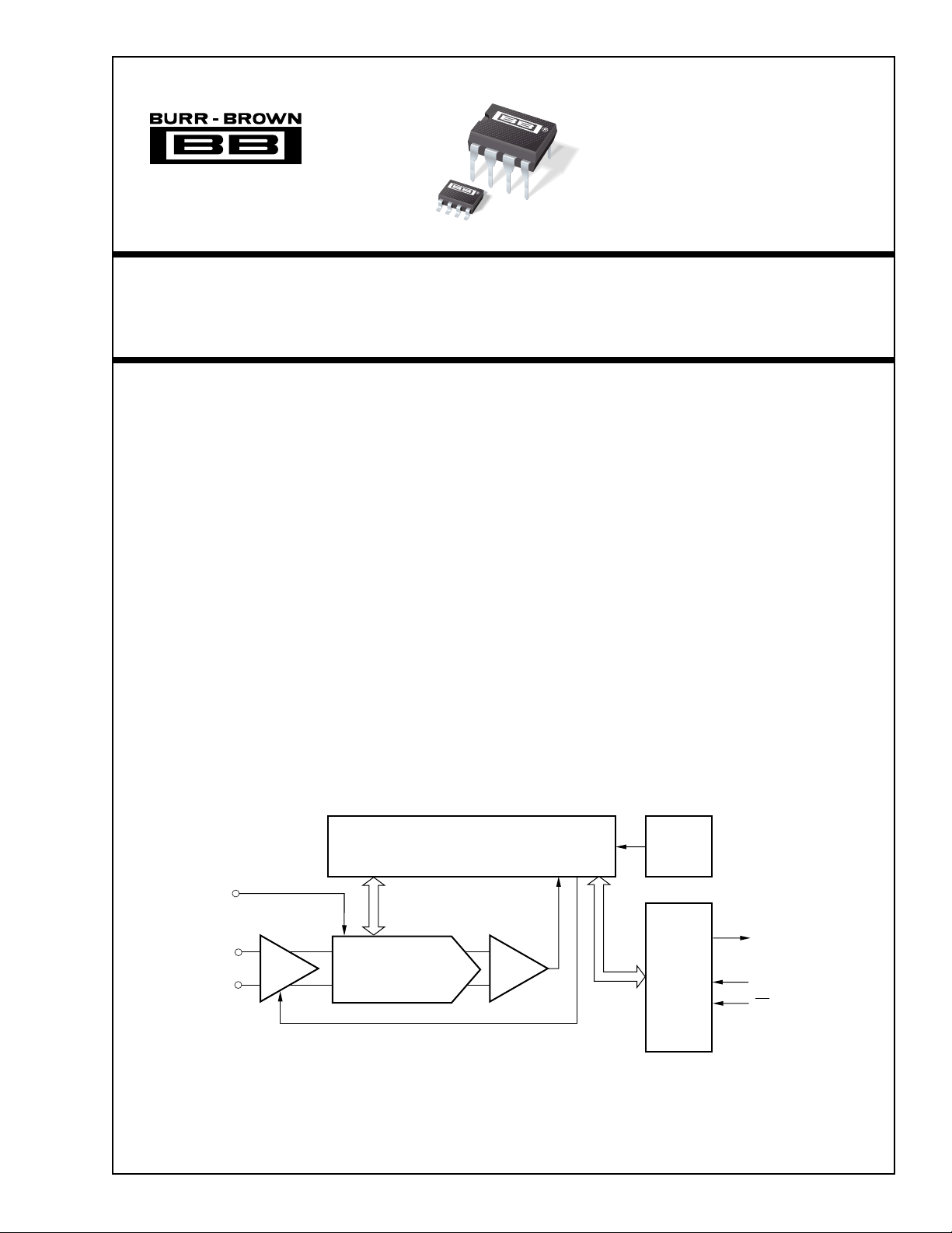
SAR
DESCRIPTION
The ADS1286 is a 12-bit, 20kHz analog-to-digital
converter with a differential input and sample and hold
amplifier and consumes only 250µA of supply current. The ADS1286 offers an SPI and SSI compatible
serial interface for communications over a two or three
wire interface. The combination of a serial two wire
interface and micropower consumption makes the
ADS1286 ideal for remote applications and for those
requiring isolation.
The ADS1286 is available in a 8-pin plastic mini DIP
and a 8-lead SOIC.
Control
SBAS053
V
REF
D
+In
–In
S/H Amp
International Airport Industrial Park • Mailing Address: PO Box 11400, Tucson, AZ 85734 • Street Address: 6730 S. Tucson Blvd., Tucson, AZ 85706 • Tel: (520) 746-1111
Twx: 910-952-1111 • Internet: http://www.burr-brown.com/ • Cable: BBRCORP • Telex: 066-6491 • FAX: (520) 889-1510 • Immediate Product Info: (800) 548-6132
©
1996 Burr-Brown Corporation PDS-1335B Printed in U.S.A. October, 1998
CDAC
Comparator
Serial
Interface
OUT
DCLOCK
CS/SHDN
Page 2
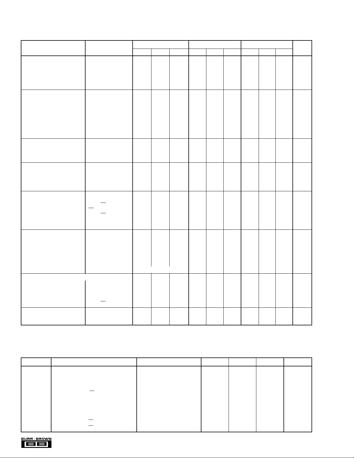
SPECIFICATIONS
At TA = T
PARAMETER CONDITIONS MIN TYP MAX MIN TYP MAX MIN TYP MAX UNITS
ANALOG INPUT
Full-Scale Input Range +In – (–In) 0 V
Absolute Input Voltage +In –0.2 V
Capacitance 25 ✻✻pF
Leakage Current ±1 ✻✻µA
SYSTEM PERFORMANCE
Resolution 12 ✻✻Bits
No Missing Codes 12 ✻✻Bits
Integral Linearity ±1 ±2 ✻✻ ±0.5 ±1 LSB
Differential Linearity ±0.5 ±1.0 ✻ ±0.75 ±0.25 ±0.75 LSB
Offset Error 0.75 ±3 ✻✻ ✻✻LSB
Gain Error ±2 ±8 ✻✻ ✻✻LSB
Noise 50 ✻✻µVrms
Power Supply Rejection 82 ✻✻dB
SAMPLING DYNAMICS
Conversion Time 12 ✻✻
Acquisition Time 1.5 ✻✻
Small Signal Bandwidth 500 ✻✻kHz
DYNAMIC CHARACTERISTICS
Total Harmonic Distortion V
SINAD V
Spurious Free Dynamic Range V
REFERENCE INPUT
REF Input Range 1.25 2.5
Input Resistance CS = V
Current Drain CS = V
DIGITAL INPUT/OUTPUT
Logic Family CMOS ✻✻
Logic Levels:
V
V
V
V
Data Format Straight Binary ✻✻
POWER SUPPLY REQUIREMENTS
Power Supply Voltage
V
CC
Quiescent Current, V
Power Down CS = V
TEMPERATURE RANGE
Specified Performance ADS1286, K, L 0 +70 ✻✻✻✻°C
✻ Specifications same as grade to the left.
to T
MIN
, +VCC = +5V, V
MAX
= +5V, f
REF
SAMPLE
= 12.5kHz, , f
CLK
= 16 • f
, unless otherwise specified.
SAMPLE
ADS1286, ADS1286A ADS1286K, ADS1286B ADS1286C, ADS1286L
REF
+0.2 ✻✻✻✻V
–In –0.2 +0.2 ✻✻✻✻V
CC
✻✻✻✻V
Clk Cycles
Clk Cycles
= 5.0Vp-p at 1kHz –85 ✻✻dB
IN
V
= 5.0Vp-p at 5kHz –83 ✻✻dB
IN
= 5.0Vp-p at 1kHz 72 ✻✻dB
IN
= 5.0Vp-p at 1kHz 90 ✻✻dB
IN
VCC+0.05V
CS = GND, f
t
≥ 640 µs, f
CYC
t
= 80µs, f
CYC
IH
IL
OH
OL
CC
= 0Hz 5000 ✻✻MΩ
CLK
CC
≤ 25kHz
CLK
= 200kHz
CLK
IIH = +5µA3 +VCC✻✻✻✻V
IIL = +5µA 0.0 0.8 ✻✻✻✻V
IOH = 250µA3 +VCC✻✻✻✻V
IOL = 250µA 0.0 0.4 ✻✻✻✻V
5000 ✻✻MΩ
0.01
2.4
2.4
2.5
20
20
✻✻✻✻✻✻V
✻✻ ✻✻µA
✻✻ ✻✻µA
✻✻ ✻✻µA
+4.50 5 5.25 ✻✻✻✻✻✻V
ANA
≥ 640µS, f
CYC
t
= 90µS, f
CYC
≤ 25kHz
CLK
= 200kHz
CLK
CC
200 400 ✻✻ ✻✻µA
250 500 ✻✻ ✻✻µA
3 ✻✻µA
t
ADS1286A, B, C –40 +85 ✻✻✻✻°C
TIMING CHARACTERISTICS
f
= 200kHz, TA = T
CLK
SYMBOL PARAMETER CONDITIONS MIN TYP MAX UNITS
t
SMPL
t
SMPL (MAX)
t
CONV
t
dDO
t
dis
t
en
t
hDO
t
f
t
r
t
CSD
t
SUCS
to T
MAX
.
MIN
Analog Input Sample Time See Operating Sequence 1.5 2.0 Clk Cycles
Maximum Sampling Frequency ADS1286 20 kHz
Conversion Time See Operating Sequence 12 Clk Cycles
Delay TIme, DCLOCK↓ to D
Delay TIme, CS↑ to D
Delay TIme, DCLOCK↓ to D
Output Data Remains Valid After DCLOCK↓ C
D
Fall Time See Test Circuits 70 100 ns
OUT
D
Rise Time See Test Circuits 60 100 ns
OUT
Data Valid See Test Circuits 85 150 ns
OUT
Hi-Z See Test Circuits 25 50 ns
OUT
Enable See Test Circuits 50 100 ns
OUT
= 100pF 15 30 ns
LOAD
Delay Time, CS↓ to DCLOCK↓ See Operating Sequence 0 ns
Delay Time, CS↓ to DCLOCK↑ See Operating Sequence 30 ns
®
ADS1286
2
Page 3
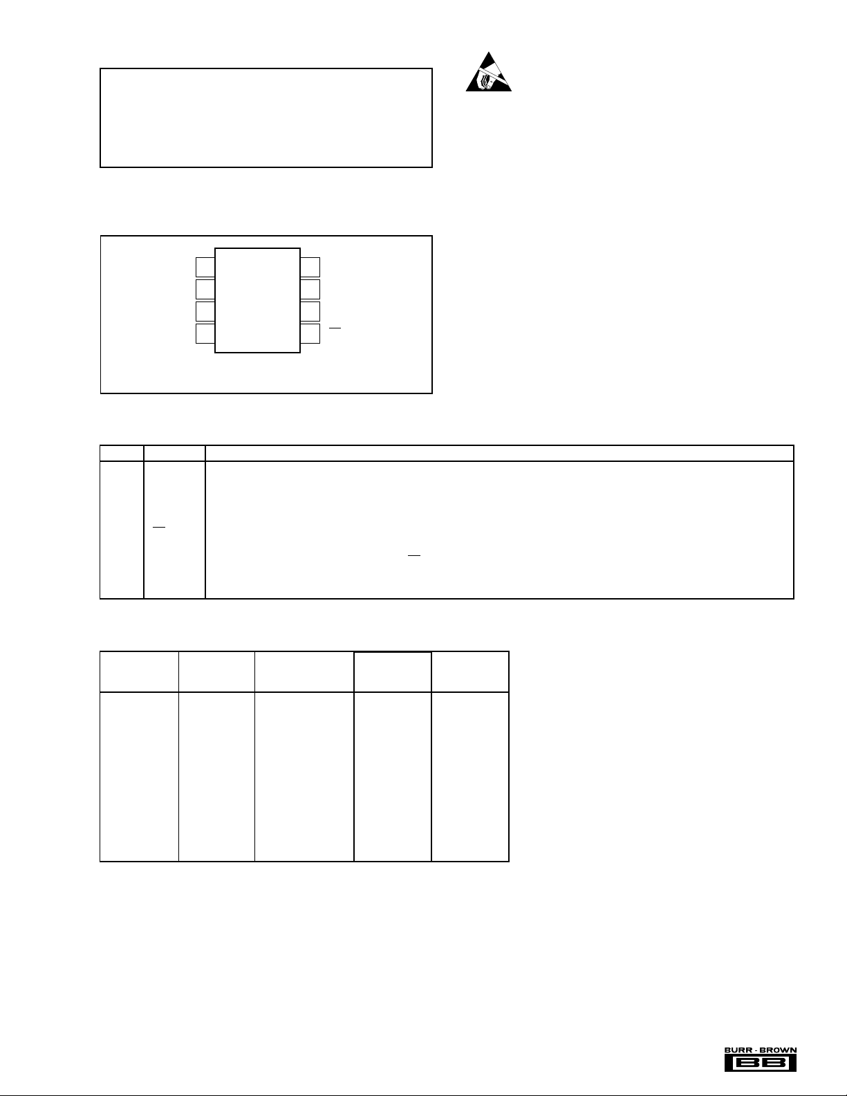
ABSOLUTE MAXIMUM RATINGS
+VCC.....................................................................................................+6V
Analog Input....................................................... –0.3V to (+V
Logic Input .........................................................–0.3V to (+V
Case Temperature ......................................................................... +100°C
Junction Temperature .................................................................... +150°C
Storage Temperature..................................................................... +125°C
External Reference Voltage .............................................................. +5.5V
NOTE: (1) Stresses above these ratings may permanently damage the device.
(1)
+ 300mV)
CC
+ 300mV)
CC
ELECTROSTATIC
DISCHARGE SENSITIVITY
Electrostatic discharge can cause damage ranging from performance degradation to complete device failure. BurrBrown Corporation recommends that all integrated circuits
be handled and stored using appropriate ESD protection
methods.
ESD damage can range from subtle performance degrada-
PIN CONFIGURATION
tion to complete device failure. Precision integrated circuits
may be more susceptible to damage because very small
parametric changes could cause the device not to meet
V
REF
+In
–In
GND
1
2
3
4
8-Pin Mini PDIP
8-Lead SOIC
ADS1286
8
7
6
5
+V
CC
DCLOCK
D
OUT
CS/SHDN
published specifications.
PIN ASSIGNMENTS
PIN NAME DESCRIPTION
1V
2 +In Non Inverting Input.
3 –In Inverting Input. Connect to ground or remote ground sense point.
4 GND Ground.
5 CS/SHDN Chip Select when low, Shutdown Mode when high.
6D
7 DCLOCK Data Clock synchronizes the serial data transfer and determines conversion speed.
8+V
REF
OUT
Reference Input.
The serial output data word is comprised of 12 bits of data. In operation the data is valid on the falling edge of DCLOCK. The
second clock pulse after the falling edge of CS enables the serial output. After one null bit the data is valid for the next 12 edges.
Power Supply.
CC
PACKAGE/ORDERING INFORMATION
PRODUCT LINEARITY RANGE PACKAGE NUMBER
INTEGRAL TEMPERATURE DRAWING
ADS1286P ±20°C to +70°C Plastic DIP 006
ADS1286PK ±20°C to +70°C Plastic DIP 006
ADS1286PL ±10°C to +70°C Plastic DIP 006
ADS1286U ±20°C to +70°C SOIC 182
ADS1286UK ±20°C to +70°C SOIC 182
ADS1286UL ±10°C to +70°C SOIC 182
ADS1286PA ±2 –40°C to +85°C Plastic DIP 006
ADS1286PB ±2 –40°C to +85°C Plastic DIP 006
ADS1286PC ±1 –40°C to +85°C Plastic DIP 006
ADS1286UA ±2 –40°C to +85°C SOIC 182
ADS1286UB ±2 –40°C to +85°C SOIC 182
ADS1286UC ±1 –40°C to +85°C SOIC 182
NOTE: (1) For detailed drawing and dimension table, please see end of data sheet, or Appendix
C of Burr-Brown IC Data Book.
The information provided herein is believed to be reliable; however, BURR-BROWN assumes no responsibility for inaccuracies or omissions. BURR-BROWN
assumes no responsibility for the use of this information, and all use of such information shall be entirely at the user’s own risk. Prices and specifications are subject
to change without notice. No patent rights or licenses to any of the circuits described herein are implied or granted to any third party. BURR-BROWN does not
authorize or warrant any BURR-BROWN product for use in life support devices and/or systems.
PACKAGE
(1)
®
3
ADS1286
Page 4
TYPICAL PERFORMANCE CURVES
At TA = +25, VCC = +5V, V
= +5V, f
REF
SAMPLE
= 12.5kHz, f
CLK
= 16 • f
, unless otherwise specified.
SAMPLE
2.5
2.0
1.5
1.0
Reference Current (µA)
0.5
0
5
4.5
4
3.5
3
2.5
2
1.5
Change in Offset (LSB)
1
0.5
0
REFERENCE CURRENT vs SAMPLE RATE
024681012
Sample Rate (kHz)
CHANGE IN OFFSET vs REFERENCE VOLTAGE
12345
Reference Voltage (V)
4.0
3.5
3.0
2.5
2.0
Reference Current (µA)
1.5
1.0
0.6
0.4
0.2
0
–0.2
Delta from 25°C (LSB)
–0.4
–0.6
REFERENCE CURRENT vs TEMPERATURE
–55 –40 –25 0 25 70 85
Temperature (°C)
CHANGE IN OFFSET vs TEMPERATURE
–55 –40 –25 0 25 70 85
Temperature (°C)
CHANGE IN INTEGRAL LINEARITY AND DIFFERENTIAL
0.10
0.05
0.00
–0.05
–0.10
–0.15
Delta from +5V Reference (LSB)
–0.20
12345
LINEARITY vs REFERENCE VOLTAGE
Change in Differential
Linearity (LSB)
Change in Integral
Linearity (LSB)
Reference Voltage (V)
®
ADS1286
CHANGE IN GAIN vs REFERENCE VOLTAGE
4
3.5
3
2.5
2
1.5
1
Change in Gain (LSB)
0.5
0
12345
Reference Voltage (V)
4
Page 5
DIFFERENTIAL LINEARITY ERROR vs CODE
3.0
2.0
1.0
0
–1.0
–2.0
–3.0
Differential Linearity Error (LSB)
0 2048 4095
Code
TYPICAL PERFORMANCE CURVES (CONT)
TOTAL HARMONIC DISTORTION vs FREQUENCY
0
–10
–20
–30
–40
–50
–60
–70
–80
–90
–100
Total Harmonic Distortion (dB)
0.1 1 10
Frequency (kHz)
At TA = +25, VCC = +5V, V
12
11.75
11.5
11.25
11
10.75
10.5
Effective Number of Bits (rms)
10.25
10
0.1 1 10
= +5V, f
REF
EFFECTIVE NUMBER OF BITS
vs REFERENCE VOLTAGE
Reference Voltage (V)
SAMPLE
= 12.5kHz, f
CLK
= 16 • f
, unless otherwise specified.
SAMPLE
SIGNAL-TO-(NOISE + DISTORTION)
100
90
80
70
60
50
40
30
20
Signal-to-(Noise + Distortion) (dB)
10
0
0.1 1 10
SIGNAL-TO-(NOISE + DISTORTION) vs INPUT LEVEL
80
70
60
50
40
30
20
10
Signal-to-(Noise + Distortion) (dB)
0
–40 –35 –30 –25 –20 –15 –10 –5 0
vs FREQUENCY
Frequency (kHz)
Input Level (dB)
SPURIOUS FREE DYNAMIC RANGE
100
and Signal-to-Noise Ratio (dB)
Spurious Free Dynamic Range
5
AND SIGNAL-TO-NOISE RATIO vs FREQUENCY
90
80
70
60
50
40
30
20
10
0
0.1 1 10
Spurious Free Dynamic Range
Signal-to-Noise Ratio
Frequency (kHz)
ADS1286
®
Page 6

TYPICAL PERFORMANCE CURVES (CONT)
At TA = +25, VCC = +5V, V
= +5V, f
REF
SAMPLE
= 12.5kHz, f
CLK
= 16 • f
, unless otherwise specified.
SAMPLE
0
–25
–50
–75
Magnitude (dB)
–100
–125
0246
POWER SUPPLY REJECTION vs RIPPLE FREQUENCY
0
–10
V
= 20mV
–20
–30
–40
–50
–60
–70
Power Supply Rejection (dB)
–80
–90
RIPPLE
1 10 100 1000 10000
4096 POINT FFT
Frequency (kHz)
Ripple Frequency (kHz)
PEAK-TO-PEAK NOISE vs REFERENCE VOLTAGE
10
9
8
7
6
5
4
3
2
Peak-to-Peak Noise (LSB)
1
0
0.1 1 10
Reference Voltage (V)
0.15
0.1
0.05
0
–0.05
Delta from 25°C (LSB)
–0.1
–0.15
–55 –40 –25 0 25 70 85
CHANGE GAIN vs TEMPERATURE
Temperature (°C)
POWER DOWN SUPPLY CURRENT
vs TEMPERATURE
3
2.5
2
1.5
1
Supply Current (µA)
0.5
0
–55 –40 –25 0 25 70 85
Temperature (°C)
®
ADS1286
400
350
300
250
200
Supply Current (µA)
150
100
–55 –40 –25 0 25 70 85
SUPPLY CURRENT vs TEMPERATURE
f
= 12.5kHz
SAMPLE
f
= 1.6kHz
SAMPLE
Temperature (°C)
6
Page 7

TYPICAL PERFORMANCE CURVES (CONT)
At TA = +25, VCC = +5V, V
= +5V, f
REF
SAMPLE
= 12.5kHz, f
CLK
= 16 • f
, unless otherwise specified.
SAMPLE
3.0
2.0
1.0
0
–1.0
–2.0
Integral Linearity Error (LSB)
–3.0
INTEGRAL LINEARITY ERROR vs CODE
0 2048 4095
Code
DIGITAL INPUT LINE THRESHOLD
vs SUPPLY VOLTAGE
3
2.5
2
1.5
1
0.5
Digital Input Threshold Voltage (V)
0
3 3.25 3.5 3.75 4 4.25 4.5 4.75 5 5.25 5.5
Supply Voltage (V)
INPUT LEAKAGE CURRENT vs TEMPERATURE
10
1
0.1
Leakage Current (nA)
0.01
–55 –40 –25 0 25 70 85
Temperature (°C)
®
7
ADS1286
Page 8

TIMING DIAGRAMS AND TEST CIRCUITS
1.4V
DCLOCK
D
OUT
Voltage Waveforms for D
CS/SHDN
D
OUT
Load Circuit for t
V
IL
t
hDO
t
dDO
3kΩ
100pF
C
LOAD
, tr, and t
dDO
Delay Times, t
OUT
Test Point
f
V
IH
dDO
V
D
OUT
t
r
Voltage Waveforms for D
Rise and Fall Times tr, and t
OUT
OH
V
OL
t
f
f
Test Point
V
CC
t
den
dis
t
dis
Waveform 2, t
Waveform 1
en
D
V
OH
V
OL
OUT
3kΩ
100pF
C
LOAD
Load Circuit for t
dis
and t
CS/SHDN
D
Waveform 1
D
Waveform 2
OUT
(1)
OUT
(2)
Voltage Waveforms for t
t
dis
dis
90%
10%
NOTES: (1) Waveform 1 is for an output with internal conditions such that
the output is HIGH unless disabled by the output control. (2) Waveform 2
is for an output with internal conditions such that the output is LOW unless
disabled by the output control.
DCLOCK
D
OUT
1
2
Voltage Waveforms for t
V
OL
B11
t
en
en
®
ADS1286
8
Page 9

CS/SHDN
1000
100
10
1
Supply Current (µA)
0.1k 1k 10k 100k
Sample Rate (kHz)
TA = 25°C
V
CC
= 5V
V
REF
= 5V
f
CLK
= 16 • f
SAMPLE
DCLOCK
D
OUT
CS/SHDN
DCLOCK
D
OUT
t
CYC
t
SUCS
t
CSD
NULL
BIT
B11
B10 B9 B8 B7 B6 B5 B4 B3 B2 B1 B0
t
SMPL
Note: (1) After completing the data transfer, if further clocks are applied with CS
LOW, the ADC will output LSB-First data then followed with zeroes indefinitely.
HI-Z HI-Z
t
SMPL
Note: (2) After completing the data transfer, if further clocks are applied with CS
LOW, the ADC will output zeroes indefinitely.
t
DATA
becomes a high impedance node, leaving the CLK running to clock out LSB-First data or zeroes.
(MSB)
t
SUCS
t
CSD
NULL
BIT
B11
B10 B9 B8 B7 B6 B5 B4 B4B3 B3B2 B2B1 B1B0
(MSB)
: During this time, the bias current and the comparator power down and the reference input
t
CONV
t
t
CONV
CYC
POWER
DOWN
NULL
HI-ZHI-Z
(1)
t
DATA
BIT
B11 B10 B9 B8
POWER DOWN
B5 B6 B7 B8 B9 B10 B11
t
DATA
(2)
FIGURE 1. ADS1286 Operating Sequence.
SERIAL INTERF ACE
The ADS1286 communicates with microprocessors and other
external digital systems via a synchronous 3-wire serial interface. DCLOCK synchronizes the data transfer with each bit
being transmitted on the falling DCLOCK edge and captured
leaving the DCLOCK running to clock out the LSB first
data or zeroes. If the CS input is not running rail-to-rail, the
input logic buffer will draw current. This current may be
large compared to the typical supply current. To obtain the
lowest supply current, bring the CS pin to ground when it is
low and to supply voltage when it is high.
on the rising DCLOCK edge in the receiving system. A falling
CS initiates data transfer as shown in Figure 1. After CS falls,
the second DCLOCK pulse enables D
the A/D conversion result is output on the D
. After one null bit,
OUT
line. Bringing
OUT
CS high resets the ADS1286 for the next data exchange.
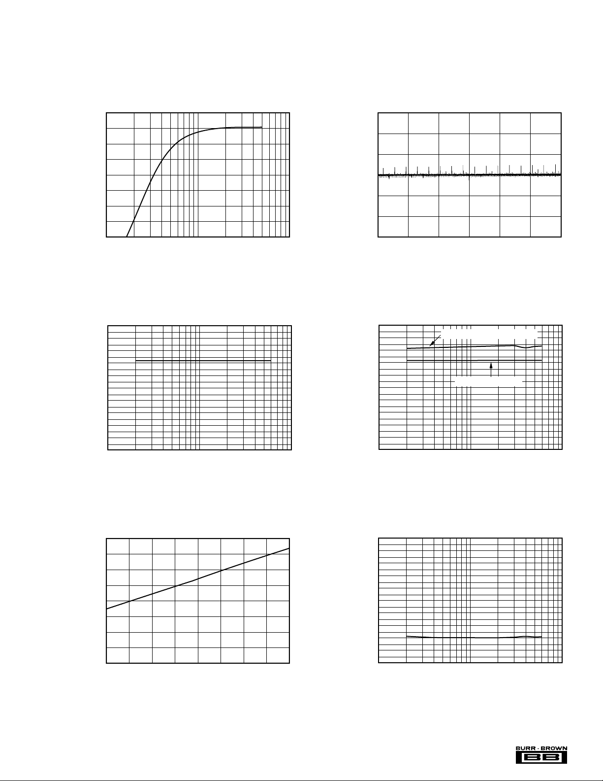
MICROPOWER OPERA TION
With typical operating currents of 250µA and automatic
shutdown between conversions, the ADS1286 achieves extremely low power consumption over a wide range of
sample rates (see Figure 2). The auto-shutdown allows the
supply current to drop with sample rate.
SHUTDOWN
The ADS1286 is equipped with automatic shutdown features. The device draws power when the CS pin is LOW and
shuts down completely when the pin is HIGH. The bias
circuit and comparator powers down and the reference input
becomes high impedance at the end of each conversion
FIGURE 2. Automatic Power Shutdown Between Conver-
sions Allows Power Consumption to Drop with
Sample Rate.
®
9
ADS1286
Page 10

MINIMIZING POWER DISSIPATION
In systems that have significant time between conversions,
the lowest power drain will occur with the minimum CS
LOW time. Bringing CS LOW, transferring data as quickly
as possible, and then bringing it back HIGH will result in the
lowest current drain. This minimizes the amount of time the
device draws power. After a conversion the A/D automatically shuts down even if CS is held LOW. If the clock is left
running to clock out LSB-data or zero, the logic will draw a
small amount of current (see Figure 3).
6.00
TA = 25°C
= +5V
V
CC
5.00
V
= +5V
REF
f
= 16 • f
CLK
4.00
3.00
2.00
Supply Current (µA)
1.00
0.00
0.1 1 10 100
SAMPLE
Sample Rate (kHz)
CS = LOW
(GND)
CS HIGH
(V
CC
)
FIGURE 3. Shutdown Current with CS HIGH is Lower than
with CS LOW.
RC INPUT FILTERING
REDUCED REFERENCE
OPERATION
The effective resolution of the ADS1286 can be increased
by reducing the input span of the converter. The ADS1286
exhibits good linearity and gain over a wide range of
reference voltages (see Typical Performance Curves “ Change
in Linearity vs Reference Voltage” and “Change in Gain vs
Reference Voltage”). However, care must be taken when
operating at low values of V
size and the resulting higher accuracy requirement placed on
the converter. The following factors must be considered
when operating at low V
1. Offset
2. Noise
OFFSET WITH REDUCED V
The offset of the ADS1286 has a larger effect on the output
code. When the ADC is operated with reduced reference
voltage. The offset (which is typically a fixed voltage)
becomes a larger fraction of an LSB as the size of the LSB
is reduced. The Typical Performance Curve “Change in
Offset vs Reference Voltage” shows how offset in LSBs is
related to reference voltage for a typical value of VOS. For
example, a VOS of 122µV which is 0.1 LSB with a 5V
reference becomes 0.5LSB with a 1V reference and 2.5LSBs
with a 0.2V reference. If this offset is unacceptable, it can be
corrected digitally by the receiving system or by offsetting
the negative input of the ADS1286.
because of the reduced LSB
REF
values:
REF
REF
It is possible to filter the inputs with an RC network as
shown in Figure 4. For large values of C
FILTER
(e.g., 1µF),
the capacitive input switching currents are averaged into a
net DC current. Therefore, a filter should be chosen with a
small resistor and large capacitor to prevent DC drops across
the resistor. The magnitude of the DC current is approximately IDC = 20pF x VIN/t
and is roughly proportional to
CYC
VIN. When running at the minimum cycle time of 64µs, the
input current equals 1.56µA at VIN = 5V. In this case, a filter
resistor of 75Ω will cause 0.1LSB of full-scale error. If a
larger filter resistor must be used, errors can be eliminated
by increasing the cycle time.
R
V
IN
FILTER
I
DC
C
FILTER
ADS1286
FIGURE 4. RC Input Filtering.
NOISE WITH REDUCED V
REF
The total input referred noise of the ADS1286 can be
reduced to approximately 200µV peak-to-peak using a ground
plane, good bypassing, good layout techniques and minimizing noise on the reference inputs. This noise is insignificant
with a 5V reference but will become a larger fraction of an
LSB as the size of the LSB is reduced.
For operation with a 5V reference, the 200µV noise is only
0.15LSB peak-to-peak. In this case, the ADS1286 noise will
contribute virtually no uncertainty to the output code. However, for reduced references, the noise may become a significant fraction of an LSB and cause undesirable jitter in the
output code. For example, with a 2.5V reference this same
200µV noise is 0.3LSB peak-to-peak. If the reference is
further reduced to 1V, the 200µV noise becomes equal to
0.8LSBs and a stable code may be difficult to achieve. In
this case averaging multiple readings may be necessary.
®
ADS1286
10
Page 11

+5V
TC
1
Thermocouple
D
1
TC
2
TC
3
ISO Thermal Block
R
1
150kΩ
R
2
59kΩ
R
4
1kΩ
1MΩ
C
10µF
+5V
R
7
10Ω
C
R
3
500kΩ
R
6
0.1µF
4
R
500Ω
5
V
REF
C
3
ADS1286
U
1
C
5
0.1µF
0.1µF
DCLOCK
D
OUT
CS/SHDN
2
OPA237
U
2
+5V
µP
3-Wire
Interface
U
4
FIGURE 5. Thermocouple Application Using a MUX to Scale the Input Range of the ADS1286.
+V
CC
C
10µF
R
8
46kΩ
0.4V
R
9
1kΩ
0.3V
R
1
MUX
1kΩ
10
0.2V
R
11
A
0
A
1
U
3
1kΩ
R
1kΩ
0.1V
12
REF200
(100µA)
RTD
FIGURE 6. ADS1286 with RTD Sensor.
2
3
V
REF
ADS1286
81
4
0.1µF
DCLOCK
D
OUT
CS/SHDN
µP
11
®
ADS1286
Page 12

PACKAGE OPTION ADDENDUM
www.ti.com
PACKAGING INFORMATION
Orderable Device Status
ADS1286P ACTIVE PDIP P 8 50 Green (RoHS &
ADS1286PA ACTIVE PDIP P 8 50 Green (RoHS &
ADS1286PB ACTIVE PDIP P 8 50 Green (RoHS &
ADS1286PBG4 ACTIVE PDIP P 8 50 Green (RoHS &
ADS1286PC ACTIVE PDIP P 8 50 Green (RoHS &
ADS1286PG4 ACTIVE PDIP P 8 50 Green (RoHS &
ADS1286PK ACTIVE PDIP P 8 50 Green (RoHS &
ADS1286PL ACTIVE PDIP P 8 50 Green (RoHS &
ADS1286U ACTIVE SOIC D 8 100 Green (RoHS &
ADS1286U/2K5 ACTIVE SOIC D 8 2500 Green (RoHS &
ADS1286U/2K5G4 ACTIVE SOIC D 8 2500 Green (RoHS &
ADS1286UA ACTIVE SOIC D 8 100 Green (RoHS &
ADS1286UA/2K5 ACTIVE SOIC D 8 2500 Green (RoHS &
ADS1286UA/2K5G4 ACTIVE SOIC D 8 2500 Green (RoHS &
ADS1286UAG4 ACTIVE SOIC D 8 100 Green (RoHS &
ADS1286UB ACTIVE SOIC D 8 100 Green (RoHS &
ADS1286UBG4 ACTIVE SOIC D 8 100 Green (RoHS &
ADS1286UC ACTIVE SOIC D 8 100 Green (RoHS &
ADS1286UCG4 ACTIVE SOIC D 8 100 Green (RoHS &
ADS1286UG4 ACTIVE SOIC D 8 100 TBD Call TI Call TI
ADS1286UK ACTIVE SOIC D 8 100 Green (RoHS &
ADS1286UKG4 ACTIVE SOIC D 8 100 Green (RoHS &
ADS1286UL ACTIVE SOIC D 8 100 Green (RoHS &
ADS1286UL/2K5 ACTIVE SOIC D 8 2500 Green (RoHS &
ADS1286ULG4 ACTIVE SOIC D 8 100 Green (RoHS &
(1)
Package
Type
Package
Drawing
Pins Package
Qty
Eco Plan
no Sb/Br)
no Sb/Br)
no Sb/Br)
no Sb/Br)
no Sb/Br)
no Sb/Br)
no Sb/Br)
no Sb/Br)
no Sb/Br)
no Sb/Br)
no Sb/Br)
no Sb/Br)
no Sb/Br)
no Sb/Br)
no Sb/Br)
no Sb/Br)
no Sb/Br)
no Sb/Br)
no Sb/Br)
no Sb/Br)
no Sb/Br)
no Sb/Br)
no Sb/Br)
no Sb/Br)
(2)
Lead/Ball Finish MSL Peak Temp
CU NIPDAU N / A for Pkg Type
CU NIPDAU N / A for Pkg Type
CU NIPDAU N / A for Pkg Type
CU NIPDAU N / A for Pkg Type
CU NIPDAU N / A for Pkg Type
CU NIPDAU N / A for Pkg Type
CU NIPDAU N / A for Pkg Type
CU NIPDAU N / A for Pkg Type
CU NIPDAU Level-2-260C-1 YEAR
CU NIPDAU Level-2-260C-1 YEAR
CU NIPDAU Level-2-260C-1 YEAR
CU NIPDAU Level-2-260C-1 YEAR
CU NIPDAU Level-2-260C-1 YEAR
CU NIPDAU Level-2-260C-1 YEAR
CU NIPDAU Level-2-260C-1 YEAR
CU NIPDAU Level-2-260C-1 YEAR
CU NIPDAU Level-2-260C-1 YEAR
CU NIPDAU Level-3-260C-168 HR
CU NIPDAU Level-3-260C-168 HR
CU NIPDAU Level-2-260C-1 YEAR
CU NIPDAU Level-2-260C-1 YEAR
CU NIPDAU Level-2-260C-1 YEAR
CU NIPDAU Level-2-260C-1 YEAR
CU NIPDAU Level-2-260C-1 YEAR
8-Aug-2006
(3)
Addendum-Page 1
Page 13

PACKAGE OPTION ADDENDUM
www.ti.com
(1)
The marketing status values are defined as follows:
8-Aug-2006
ACTIVE: Product device recommended for new designs.
LIFEBUY: TI has announced that the device will be discontinued, and a lifetime-buy period is in effect.
NRND: Not recommended for new designs. Device is in production to support existing customers, but TI does not recommend using this part in
a new design.
PREVIEW: Device has been announced but is not in production. Samples may or may not be available.
OBSOLETE: TI has discontinued the production of the device.
(2)
Eco Plan - The planned eco-friendly classification: Pb-Free (RoHS), Pb-Free (RoHS Exempt), or Green (RoHS & no Sb/Br) - please check
http://www.ti.com/productcontent for the latest availability information and additional product content details.
TBD: The Pb-Free/Green conversion plan has not been defined.
Pb-Free (RoHS): TI's terms "Lead-Free" or "Pb-Free" mean semiconductor products that are compatible with the current RoHS requirements
for all 6 substances, including the requirement that lead not exceed 0.1% by weight in homogeneous materials. Where designed to be soldered
at high temperatures, TI Pb-Free products are suitable for use in specified lead-free processes.
Pb-Free (RoHS Exempt): This component has a RoHS exemption for either 1) lead-based flip-chip solder bumps used between the die and
package, or 2) lead-based die adhesive used between the die and leadframe. The component is otherwise considered Pb-Free (RoHS
compatible) as defined above.
Green (RoHS & no Sb/Br): TI defines "Green" to mean Pb-Free (RoHS compatible), and free of Bromine (Br) and Antimony (Sb) based flame
retardants (Br or Sb do not exceed 0.1% by weight in homogeneous material)
(3)
MSL, Peak Temp. -- The Moisture Sensitivity Level rating according to the JEDEC industry standard classifications, and peak solder
temperature.
Important Information and Disclaimer:The information provided on this page represents TI's knowledge and belief as of the date that it is
provided. TI bases its knowledge and belief on information provided by third parties, and makes no representation or warranty as to the
accuracy of such information. Efforts are underway to better integrate information from third parties. TI has taken and continues to take
reasonable steps to provide representative and accurate information but may not have conducted destructive testing or chemical analysis on
incoming materials and chemicals. TI and TI suppliers consider certain information to be proprietary, and thus CAS numbers and other limited
information may not be available for release.
In no event shall TI's liability arising out of such information exceed the total purchase price of the TI part(s) at issue in this document sold by TI
to Customer on an annual basis.
Addendum-Page 2
Page 14

IMPORTANT NOTICE
Texas Instruments Incorporated and its subsidiaries (TI) reserve the right to make corrections, modifications,
enhancements, improvements, and other changes to its products and services at any time and to discontinue
any product or service without notice. Customers should obtain the latest relevant information before placing
orders and should verify that such information is current and complete. All products are sold subject to TI’s terms
and conditions of sale supplied at the time of order acknowledgment.
TI warrants performance of its hardware products to the specifications applicable at the time of sale in
accordance with TI’s standard warranty. Testing and other quality control techniques are used to the extent TI
deems necessary to support this warranty . Except where mandated by government requirements, testing of all
parameters of each product is not necessarily performed.
TI assumes no liability for applications assistance or customer product design. Customers are responsible for
their products and applications using TI components. To minimize the risks associated with customer products
and applications, customers should provide adequate design and operating safeguards.
TI does not warrant or represent that any license, either express or implied, is granted under any TI patent right,
copyright, mask work right, or other TI intellectual property right relating to any combination, machine, or process
in which TI products or services are used. Information published by TI regarding third-party products or services
does not constitute a license from TI to use such products or services or a warranty or endorsement thereof.
Use of such information may require a license from a third party under the patents or other intellectual property
of the third party, or a license from TI under the patents or other intellectual property of TI.
Reproduction of information in TI data books or data sheets is permissible only if reproduction is without
alteration and is accompanied by all associated warranties, conditions, limitations, and notices. Reproduction
of this information with alteration is an unfair and deceptive business practice. TI is not responsible or liable for
such altered documentation.
Resale of TI products or services with statements different from or beyond the parameters stated by TI for that
product or service voids all express and any implied warranties for the associated TI product or service and
is an unfair and deceptive business practice. TI is not responsible or liable for any such statements.
Following are URLs where you can obtain information on other Texas Instruments products and application
solutions:
Products Applications
Amplifiers amplifier.ti.com Audio www.ti.com/audio
Data Converters dataconverter.ti.com Automotive www.ti.com/automotive
DSP dsp.ti.com Broadband www.ti.com/broadband
Interface interface.ti.com Digital Control www.ti.com/digitalcontrol
Logic logic.ti.com Military www.ti.com/military
Power Mgmt power.ti.com Optical Networking www.ti.com/opticalnetwork
Microcontrollers microcontroller.ti.com Security www.ti.com/security
Low Power Wireless www.ti.com/lpw Telephony www.ti.com/telephony
Video & Imaging www.ti.com/video
Wireless www.ti.com/wireless
Mailing Address: Texas Instruments
Post Office Box 655303 Dallas, Texas 75265
Copyright 2006, Texas Instruments Incorporated
 Loading...