
ADS1274
ADS1278
1
FEATURES
DESCRIPTION
APPLICATIONS
VREFP VREFN AVDD DVDD
TEST[1:0]
FORMAT[2:0]
CLK
SYNC
PWDN[8:1]
CLKDIV
Control
Logic
SPI
and
Frame-
Sync
Interface
IOVDD
DGNDAGND
DRDY/FSYNC
SCLK
DOUT[8:1]
DIN
Input2
Input1
Input4
Input3
Input6
Input5
Input8
Input7
DS
DS
DS
DS
DS
DS
DS
DS
PWDN[4:1]
ADS1278
Four
Digital
Filters
AVDD DVDD
TEST[1:0]
FORMAT[2:0]
CLK
SYNC
CLKDIV
Control
Logic
SPI
and
Frame-
Sync
Interface
IOVDD
DGNDAGND
DRDY/FSYNC
SCLK
DOUT[4:1]
DIN
ADS1274
MODE[1:0]
MODE[1:0]
Eight
Digital
Filters
VREFP VREFN
Input2
Input1
Input4
Input3
DS
DS
DS
DS
ADS1274
ADS1278
www.ti.com
SBAS367 – JUNE 2007
Quad/Octal, Simultaneous Sampling, 24-Bit Analog-to-Digital Converters
234
• Simultaneously Measure Four/Eight Channels
• Up to 128kSPS Data Rate
Based on the single-channel ADS1271 , the ADS1274
(quad) and ADS1278 (octal) are 24-bit, delta-sigma
• AC Performance:
( Δ Σ ) analog-to-digital converters (ADCs) with data
62kHz Bandwidth
rates up to 128k samples per second (SPS), allowing
111dB SNR (High-Resolution Mode)
simultaneous sampling of four or eight channels. The
– 108dB THD
devices are offered in identical packages, permitting
• DC Accuracy:
drop-in expandability.
0.8 μ V/ ° C Offset Drift
Traditionally, industrial delta-sigma ADCs offering
1.3ppm/ ° C Gain Drift
good drift performance use digital filters with large
• Selectable Operating Modes:
passband droop. As a result, they have limited signal
High-Speed: 128kSPS, 106dB SNR
bandwidth and are mostly suited for dc
High-Resolution: 52kSPS, 111dB SNR measurements. High-resolution ADCs in audio
applications offer larger usable bandwidths, but the
Low-Power: 52kSPS, 31mW/ch
offset and drift specifications are significantly weaker
Low-Speed: 10kSPS, 7mW/ch
than respective industrial counterparts. The ADS1274
• Linear Phase Digital Filter
and ADS1278 combine these types of converters,
• SPI™ or Frame-Sync Serial Interface
allowing high-precision industrial measurement with
excellent dc and ac specifications.
• Low Sampling Aperture Error
• Modulator Output Option (digital filter bypass)
The high-order, chopper-stabilized modulator
achieves very low drift with low in-band noise. The
• Analog Supply: 5V
onboard decimation filter suppresses modulator and
• Digital Core: 1.8V
signal out-of-band noise. These ADCs provide a
• I/O Supply: 1.8V to 3.3V
usable signal bandwidth up to 90% of the Nyquist
rate with less than 0.005dB of ripple.
Four operating modes allow for optimization of speed,
• Vibration/Modal Analysis
resolution, and power. All operations are controlled
• Multi-Channel Data Acquisition
directly by pins; there are no registers to program.
The devices are fully specified over the extended
• Acoustics/Dynamic Strain Gauges
industrial range ( – 40 ° C to +105 ° C) and are available
• Pressure Sensors
in an HTQFP-64 PowerPAD™ package.
1
Please be aware that an important notice concerning availability, standard warranty, and use in critical applications of
Texas Instruments semiconductor products and disclaimers thereto appears at the end of this data sheet.
2 PowerPAD is a trademark of Texas Instruments, Inc.
3 SPI is a trademark of Motorola, Inc.
4 All other trademarks are the property of their respective owners.
PRODUCTION DATA information is current as of publication date.
Copyright © 2007, Texas Instruments Incorporated
Products conform to specifications per the terms of the Texas
Instruments standard warranty. Production processing does not
necessarily include testing of all parameters.
www.ti.com
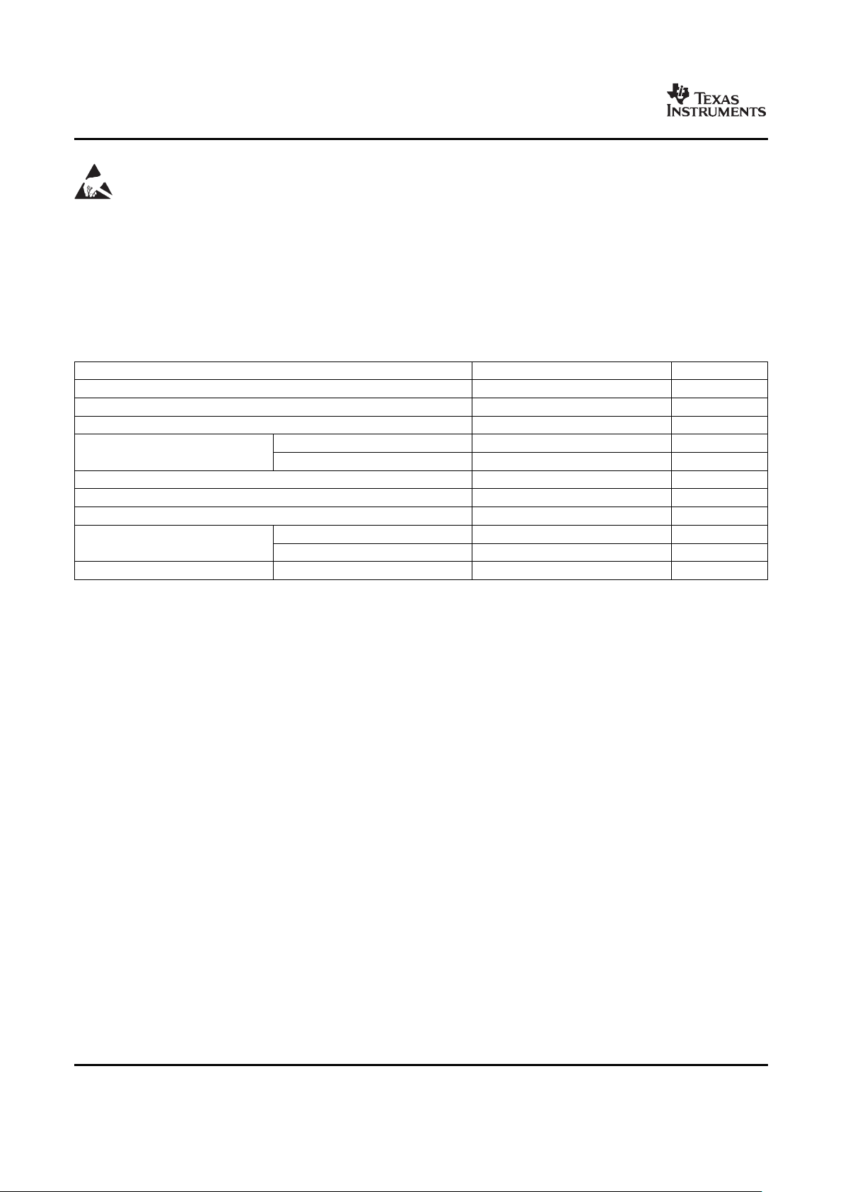
ABSOLUTE MAXIMUM RATINGS
ADS1274
ADS1278
SBAS367 – JUNE 2007
This integrated circuit can be damaged by ESD. Texas Instruments recommends that all integrated circuits be handled with
appropriate precautions. Failure to observe proper handling and installation procedures can cause damage.
ESD damage can range from subtle performance degradation to complete device failure. Precision integrated circuits may be more
susceptible to damage because very small parametric changes could cause the device not to meet its published specifications.
ORDERING INFORMATION
For the most current package and ordering information, see the Package Option Addendum at the end of this
document, or see the TI web site at www.ti.com .
Over operating free-air temperature range unless otherwise noted
(1)
ADS1274, ADS1278 UNIT
AVDD to AGND – 0.3 to +6.0 V
DVDD, IOVDD to DGND – 0.3 to +3.6 V
AGND to DGND – 0.3 to +0.3 V
Momentary 100 mA
Input current
Continuous 10 mA
Analog input to AGND – 0.3 to AVDD + 0.3 V
Digital input or output to DGND – 0.3 to DVDD + 0.3 V
Maximum junction temperature +150 ° C
ADS1274 – 40 to +125 ° C
Operating temperature range
ADS1278 – 40 to +105 ° C
Storage temperature range – 60 to +150 ° C
(1) Stresses above these ratings may cause permanent damage. Exposure to absolute maximum conditions for extended periods may
degrade device reliability. These are stress ratings only, and functional operation of the device at these or any other conditions beyond
those specified is not implied.
2
Copyright © 2007, Texas Instruments Incorporated
Submit Documentation Feedback
Product Folder Link(s): ADS1274 ADS1278
www.ti.com
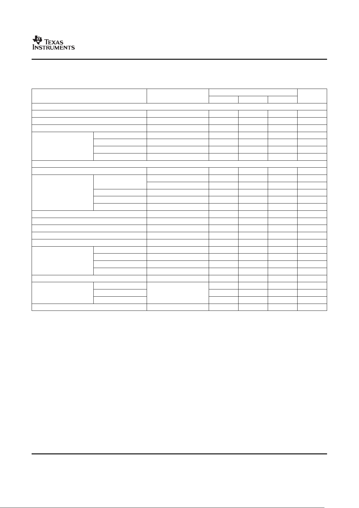
ELECTRICAL CHARACTERISTICS
ADS1274
ADS1278
SBAS367 – JUNE 2007
All specifications at TA= – 40 ° C to +105 ° C, AVDD = +5V, DVDD = +1.8V, IOVDD = +3.3V, f
CLK
= 27MHz, VREFP = 2.5V,
VREFN = 0V, and all channels active, unless otherwise noted.
ADS1274, ADS1278
PARAMETER TEST CONDITIONS MIN TYP MAX UNIT
Analog Inputs
Full-scale input voltage (FSR
(1)
) VIN= (AINP – AINN) ± V
REF
V
Absolute input voltage AINP or AINN to AGND AGND – 0.1 AVDD + 0.1 V
Common-mode input voltage (V
CM
) VCM= (AINP + AINN)/2 2.5 V
High-Speed mode 14 k Ω
High-Resolution mode 14 k Ω
Differential input impedance
Low-Power mode 28 k Ω
Low-Speed mode 140 k Ω
DC Performance
Resolution No missing codes 24 Bits
f
CLK
= 32.768MHz
(2)
128,000 SPS
High-Speed mode
f
CLK
= 27MHz 105,469 SPS
(3)
Data rate (f
DATA
) High-Resolution mode 52,734 SPS
Low-Power mode 52,734 SPS
Low-Speed mode 10,547 SPS
Integral nonlinearity (INL)
(4)
Differential input, VCM= 2.5V ± 0.0003 ± 0.0012 % FSR
(1)
Offset error 0.25 2 mV
Offset drift 0.8 μ V/ ° C
Gain error 0.1 0.5 % FSR
Gain drift 1.3 ppm/ ° C
High-Speed mode Shorted input 8.5 16 μ V, rms
High-Resolution mode Shorted input 5.5 12 μ V, rms
Noise
Low-Power mode Shorted input 8.5 16 μ V, rms
Low-Speed mode Shorted input 8.0 16 μ V, rms
Common-mode rejection fCM= 60Hz 90 108 dB
AVDD 80 dB
Power-supply rejection DVDD fPS= 60Hz 85 dB
IOVDD 105 dB
V
COM
output voltage No load AVDD/2 V
(1) FSR = full-scale range = 2V
REF
.
(2) f
CLK
= 32.768MHz max for High-Speed mode, and 27MHz max for all other modes. When f
CLK
> 27MHz, operation is limited to
Frame-Sync mode and V
REF
≤ 2.6V.
(3) SPS = samples per second.
(4) Best fit method.
3
Copyright © 2007, Texas Instruments Incorporated
Submit Documentation Feedback
Product Folder Link(s): ADS1274 ADS1278
www.ti.com
ADS1274
ADS1278
SBAS367 – JUNE 2007
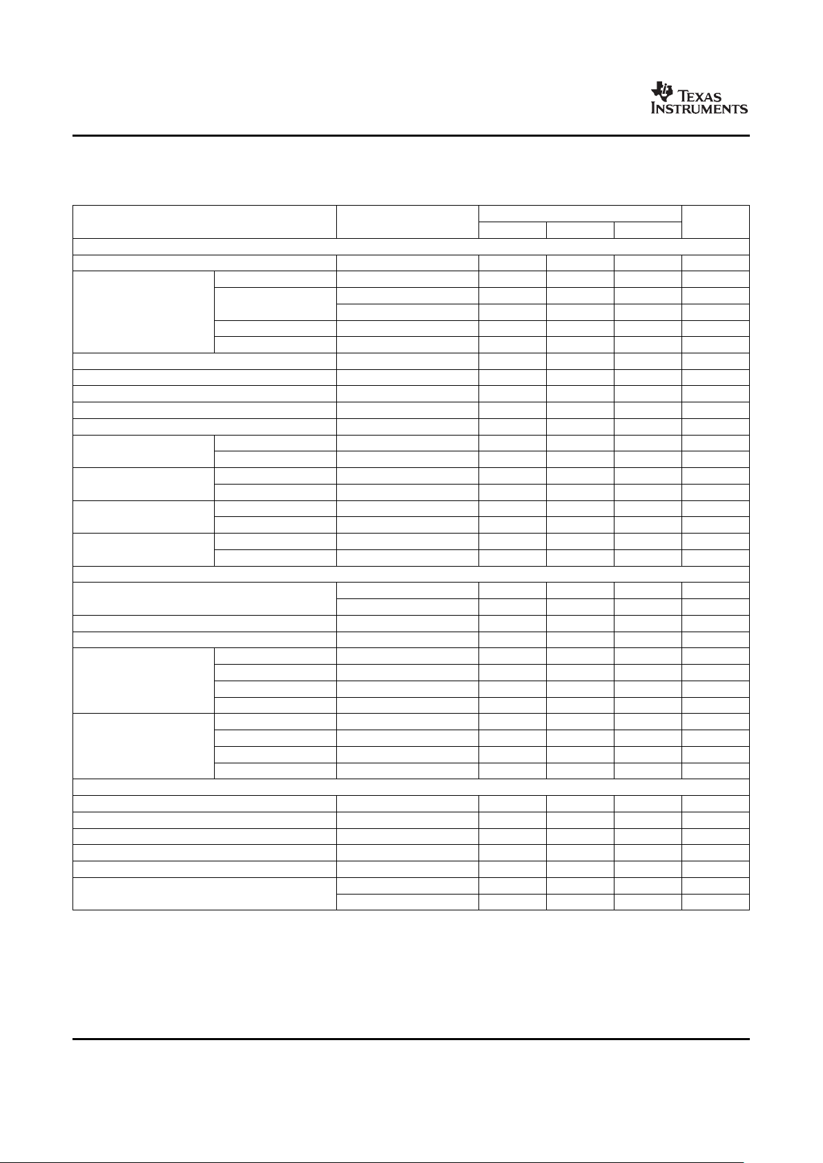
ELECTRICAL CHARACTERISTICS (continued)
All specifications at TA= – 40 ° C to +105 ° C, AVDD = +5V, DVDD = +1.8V, IOVDD = +3.3V, f
CLK
= 27MHz, VREFP = 2.5V,
VREFN = 0V, and all channels active, unless otherwise noted.
ADS1274, ADS1278
PARAMETER TEST CONDITIONS MIN TYP MAX UNIT
AC Performance
Crosstalk f = 1kHz, – 0.5dBFS
(5)
– 107 dB
High-Speed mode 101 106 dB
V
REF
= 2.5V 103 110 dB
High-Resolution mode
Signal-to-noise ratio (SNR)
(6)
V
REF
= 3V 111 dB
(unweighted)
Low-Power mode 101 106 dB
Low-Speed mode 101 107 dB
Total harmonic distortion (THD)
(7)
VIN= 1kHz, – 0.5dBFS – 108 – 96 dB
Spurious-free dynamic range 109 dB
Passband ripple ± 0.005 dB
Passband 0.453 f
DATA
Hz
– 3dB Bandwidth 0.49 f
DATA
Hz
High-Resolution mode 95 dB
Stop band attenuation
All other modes 100
High-Resolution mode 0.547 f
DATA
127.453 f
DATA
Hz
Stop band
All other modes 0.547 f
DATA
63.453 f
DATA
Hz
High-Resolution mode 39/f
DATA
s
Group delay
All other modes 38/f
DATA
s
High-Resolution mode Complete settling 78/f
DATA
s
Settling time (latency)
All other modes Complete settling 76/f
DATA
s
Voltage Reference Inputs
f
CLK
= 27MHz 0.5 2.5 3.1 V
Reference input voltage (V
REF
)
(V
REF
= VREFP – VREFN)
f
CLK
= 32.768MHz
(8)
0.5 2.5 2.6 V
Negative reference input (VREFN) AGND – 0.1 AGND + 0.1 V
Positive reference input (VREFP) VREFN + 0.5 AVDD + 0.1 V
High-Speed mode 1.3 k Ω
High-Resolution mode 1.3 k Ω
ADS1274
Reference Input impedance
Low-Power mode 2.6 k Ω
Low-Speed mode 13 k Ω
High-Speed mode 0.65 k Ω
High-Resolution mode 0.65 k Ω
ADS1278
Reference Input impedance
Low-Power mode 1.3 k Ω
Low-Speed mode 6.5 k Ω
Digital Input/Output (IOVDD = 1.8V to 3.6V)
V
IH
0.7 IOVDD IOVDD V
V
IL
DGND 0.3 IOVDD V
V
OH
IOH= 4mA 0.8 IOVDD IOVDD V
V
OL
IOL= 4mA DGND 0.2 IOVDD V
Input leakage 0 < V
IN DIGITAL
< IOVDD ± 10 μ A
High-Speed mode
(8)
0.1 32.768 MHz
Master clock rate (f
CLK
)
Other modes 0.1 27 MHz
(5) Worst-case channel crosstalk between one or more channels.
(6) Minimum SNR is ensured by the limit of the DC noise specification.
(7) THD includes the first nine harmonics of the input signal; Low-Speed mode includes the first five harmonics.
(8) f
CLK
= 32.768MHz max for High-Speed mode, and 27MHz max for all other modes. When f
CLK
> 27MHz, operation is limited to
Frame-Sync mode and V
REF
≤ 2.6V.
4
Copyright © 2007, Texas Instruments Incorporated
Submit Documentation Feedback
Product Folder Link(s): ADS1274 ADS1278
www.ti.com
ADS1274
ADS1278
SBAS367 – JUNE 2007
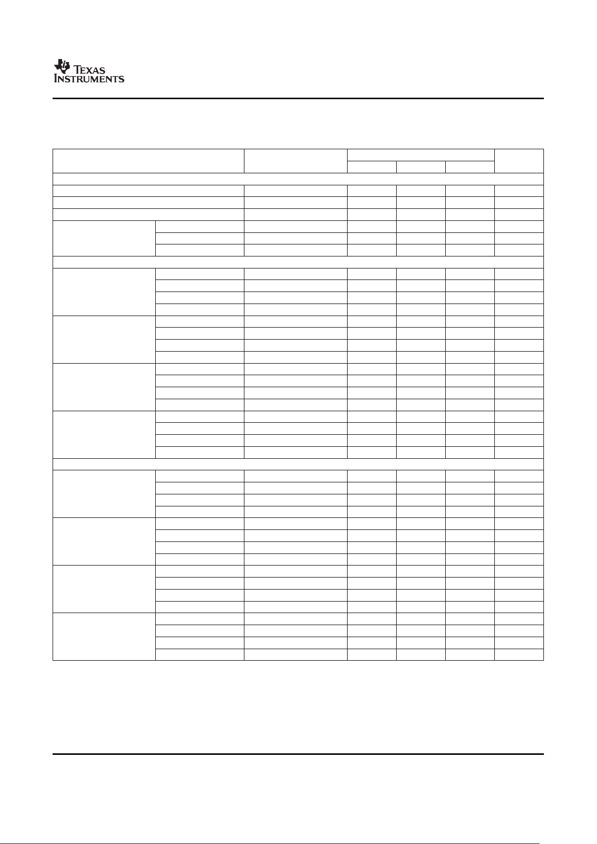
ELECTRICAL CHARACTERISTICS (continued)
All specifications at TA= – 40 ° C to +105 ° C, AVDD = +5V, DVDD = +1.8V, IOVDD = +3.3V, f
CLK
= 27MHz, VREFP = 2.5V,
VREFN = 0V, and all channels active, unless otherwise noted.
ADS1274, ADS1278
PARAMETER TEST CONDITIONS MIN TYP MAX UNIT
Power Supply
AVDD 4.75 5 5.25 V
DVDD 1.65 1.8 1.95 V
IOVDD 1.65 3.6 V
AVDD 1 10 μ A
Power-down current DVDD 1 15 μ A
IOVDD 1 10 μ A
ADS1274
High-Speed mode 50 75 mA
High-Resolution mode 50 75 mA
ADS1274
AVDD current
Low-Power mode 23 35 mA
Low-Speed mode 5 9 mA
High-Speed mode 18 24 mA
High-Resolution mode 12 17 mA
ADS1274
DVDD current
Low-Power mode 10 15 mA
Low-Speed mode 2.5 4.5 mA
High-Speed mode 0.15 0.5 mA
High-Resolution mode 0.075 0.3 mA
ADS1274
IOVDD current
Low-Power mode 0.075 0.3 mA
Low-Speed mode 0.02 0.15 mA
High-Speed mode 285 420 mW
High-Resolution mode 275 410 mW
ADS1274
Power dissipation
Low-Power mode 135 210 mW
Low-Speed mode 30 55 mW
ADS1278
High-Speed mode 97 145 mA
High-Resolution mode 97 145 mA
ADS1278
AVDD current
Low-Power mode 44 64 mA
Low-Speed mode 9 14 mA
High-Speed mode 23 30 mA
High-Resolution mode 16 20 mA
ADS1278
DVDD current
Low-Power mode 12 17 mA
Low-Speed mode 2.5 4.5 mA
High-Speed mode 0.25 1 mA
High-Resolution mode 0.125 0.5 mA
ADS1278
IOVDD current
Low-Power mode 0.125 0.5 mA
Low-Speed mode 0.035 0.2 mA
High-Speed mode 530 785 mW
High-Resolution mode 515 765 mW
ADS1278
Power dissipation
Low-Power mode 245 355 mW
Low-Speed mode 50 80 mW
5
Copyright © 2007, Texas Instruments Incorporated
Submit Documentation Feedback
Product Folder Link(s): ADS1274 ADS1278
www.ti.com
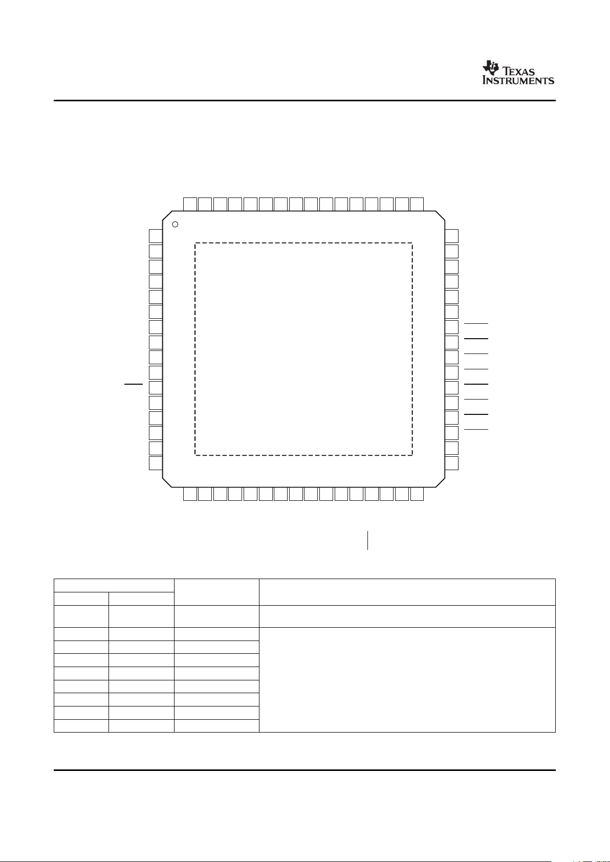
ADS1274/ADS1278 PIN ASSIGNMENTS
AINN7
(1)
AINP7
(1)
AINN8
(1)
AINP8
(1)
AVDD
AGND
PWDN1
PWDN2
PWDN3
PWDN4
PWDN5
(1)
PWDN6
(1)
PWDN7
(1)
PWDN8
(1)
MODE0
MODE1
AINP2
AINN2
AINP1
AINN1
AVDD
AGND
DGND
TEST0
TEST1
CLKDIV
SYNC
DIN
DOUT8
(1)
DOUT7
(1)
DOUT6
(1)
DOUT5
(1)
AINN3
AINP3
AINN4
AINP4
AVDD
AGND
VREFN
VREFP
VCOM
AGND
AVDD
AINP5
(1)
AINN6
(1)
AINP6
(1)
AINN5
(1)
DOUT4
DOUT3
DOUT2
DOUT1
DGND
IOVDD
IOVDD
DGND
DGND
DVDD
CLK
SCLK
DRDY
/FSYNC
FORMAT2
FORMAT1
FORMAT0
ADS1274/ADS1278
AGND
1
2
3
4
5
6
7
8
9
10
11
12
13
14
15
16
48
47
46
45
44
43
42
41
40
39
38
37
36
35
34
33
17
18
19
20
21
22
23
24
25
26
27
28
29
30
31
32
64
63
62
61
60
59
58
57
56
55
54
53
52
51
50
49
(PowerPADOutline)
NOTE:(1) pinnamesindicateadditionalpinsforBoldface
theADS1278;seepindescriptions.
ADS1274
ADS1278
SBAS367 – JUNE 2007
PAP PACKAGE
HTQFP-64
(TOP VIEW)
ADS1274/ADS1278 PIN DESCRIPTIONS
PIN
NAME NO. FUNCTION DESCRIPTION
6, 43, 54,
AGND Analog ground Analog ground; connect to DGND using a single plane.
58, 59
AINP1 3 Analog input
AINP2 1 Analog input
AINP3 63 Analog input ADS1278: AINP[8:1] Positive analog input, channels 8 through 1.
AINP4 61 Analog input
AINP5 51 Analog input ADS1274: AINP[8:5] Connected to internal ESD rails. The inputs may float.
AINP[4:1] Positive analog input, channels 4 through 1.
AINP6 49 Analog input
AINP7 47 Analog input
AINP8 45 Analog input
6
Copyright © 2007, Texas Instruments Incorporated
Submit Documentation Feedback
Product Folder Link(s): ADS1274 ADS1278
www.ti.com
ADS1274
ADS1278
SBAS367 – JUNE 2007
ADS1274/ADS1278 PIN DESCRIPTIONS (continued)
PIN
NAME NO. FUNCTION DESCRIPTION
AINN1 4 Analog input
AINN2 2 Analog input
AINN3 64 Analog input ADS1278: AINN[8:1] Negative analog input, channels 8 through 1.
AINN4 62 Analog input
AINN5 52 Analog input ADS1274: AINN[8:5] Connected to internal ESD rails. The inputs may float.
AINN[4:1] Negative analog input, channels 4 through 1.
AINN6 50 Analog input
AINN7 48 Analog input
AINN8 46 Analog input
AVDD 5, 44, 53, 60 Analog power supply Analog power supply (4.75V to 5.25V).
VCOM 55 Analog output AVDD/2 Unbuffered voltage output.
VREFN 57 Analog input Negative reference input.
VREFP 56 Analog input Positive reference input.
CLK 27 Digital input Master clock input.
CLK input divider control: 1 = 32.768MHz (High-Speed mode only) / 27MHz
CLKDIV 10 Digital input
0 = 13.5MHz (low-power) / 5.4MHz (low-speed)
DGND 7, 21, 24, 25 Digital ground Digital ground power supply.
DIN 12 Digital input Daisy-chain data input.
DOUT1 20 Digital output DOUT1 is TDM data output (TDM mode).
DOUT2 19 Digital output
DOUT3 18 Digital output ADS1278: DOUT[8:1] Data output for channels 8 through 1.
DOUT4 17 Digital output
DOUT5 16 Digital output ADS1274: DOUT[8:5] Internally connected to active circuitry; outputs are
driven.
DOUT6 15 Digital output
DOUT[4:1] Data output for channels 4 through 1.
DOUT7 14 Digital output
DOUT8 13 Digital output
DRDY/
29 Digital input/output Frame-Sync protocol: frame clock input; SPI protocol: data ready output.
FSYNC
DVDD 26 Digital power supply Digital core power supply (+1.65V to +1.95V).
FORMAT0 32 Digital input
FORMAT[2:0] Selects Frame-Sync/SPI protocol, TDM/discrete data outputs,
FORMAT1 31 Digital input
fixed/dynamic position TDM data, and modulator mode/normal operating mode.
FORMAT2 30 Digital input
IOVDD 22, 23 Digital power supply I/O power supply (+1.65V to +3.6V).
MODE0 34 Digital input
MODE[1:0] Selects High-Speed, High-Resolution, Low-Power, or Low-Speed
mode operation.
MODE1 33 Digital input
PWDN1 42 Digital input
PWDN2 41 Digital input
PWDN3 40 Digital input ADS1278: PWDN[8:1] Power-down control for channels 8 through 1.
PWDN4 39 Digital input
PWDN5 38 Digital input ADS1274: PWDN[8:5] must = 0V.
PWDN[4:1] Power-down control for channels 4 through 1.
PWDN6 37 Digital input
PWDN7 36 Digital input
PWDN8 35 Digital input
SCLK 28 Digital input/output Serial clock input, Modulator clock output.
SYNC 11 Digital input Synchronize input (all channels).
TEST0 8 Digital input TEST[1:0] Test mode select: 00 = Normal operation 01 = Do not use
11 = Boundary scan test 10 = Do not use
TEST1 9 Digital input
mode
7
Copyright © 2007, Texas Instruments Incorporated
Submit Documentation Feedback
Product Folder Link(s): ADS1274 ADS1278
www.ti.com
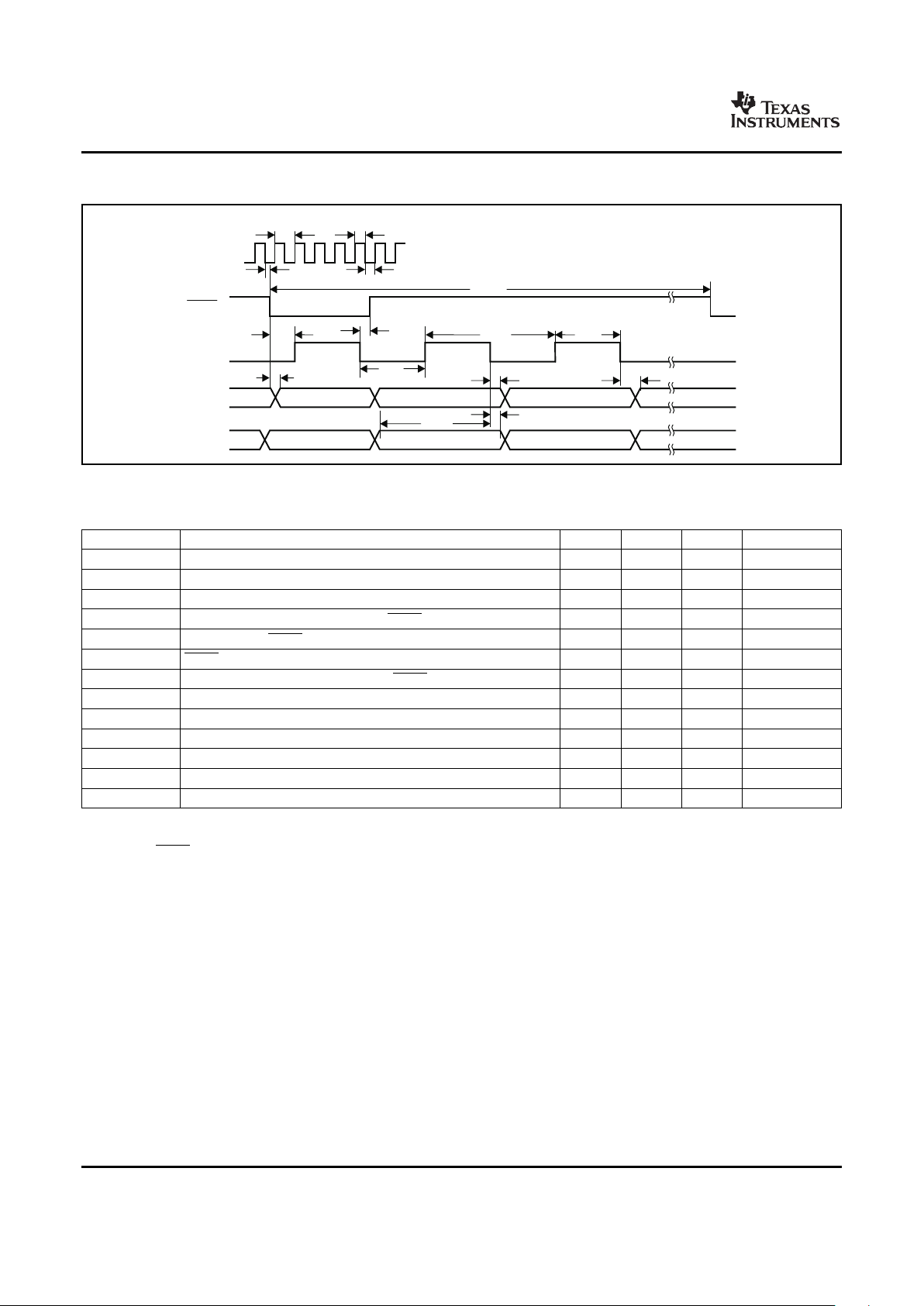
CLK
t
CPW
t
CLK
t
CPW
t
SD
t
SCLK
t
DIST
t
DOHD
t
SPW
Bit23(MSB) Bit22 Bit21
t
SPW
t
DOPD
t
CD
t
DS
t
MSBPD
t
DIHD
· · ·
t
CONV
DRDY
SCLK
DOUT
DIN
TIMING REQUIREMENTS: SPI FORMAT
ADS1274
ADS1278
SBAS367 – JUNE 2007
TIMING CHARACTERISTICS: SPI FORMAT
For TA= – 40 ° C to +105 ° C, IOVDD = 1.65V to 3.6V, and DVDD = 1.65V to 1.95V.
SYMBOL PARAMETER MIN TYP MAX UNIT
t
CLK
CLK period (1/f
CLK
)
(1)
37 10,000 ns
t
CPW
CLK positive or negative pulse width 15 ns
t
CONV
Conversion period (1/f
DATA
)
(2)
256 2560 t
CLK
t
CD
(3)
Falling edge of CLK to falling edge of DRDY 22 ns
t
DS
(3)
Falling edge of DRDY to rising edge of first SCLK to retrieve data 1 t
CLK
t
MSBPD
DRDY falling edge to DOUT MSB valid (propagation delay) 16 ns
t
SD
(3)
Falling edge of SCLK to rising edge of DRDY 18 ns
t
SCLK
(4)
SCLK period 1 t
CLK
t
SPW
SCLK positive or negative pulse width 0.4 t
CLK
t
DOHD
(3) (5)
SCLK falling edge to new DOUT invalid (hold time) 10 ns
t
DOPD
(3)
SCLK falling edge to new DOUT valid (propagation delay) 32 ns
t
DIST
New DIN valid to falling edge of SCLK (setup time) 6 ns
t
DIHD
(5)
Old DIN valid to falling edge of SCLK (hold time) 6 ns
(1) f
CLK
= 27MHz maximum.
(2) Depends on MODE[1:0] and CLKDIV selection. See Table 6 (f
CLK
/f
DATA
).
(3) Load on DRDY and DOUT = 20pF.
(4) For best performance, limit f
SCLK
/f
CLK
to ratios of 1, 1/2, 1/4, 1/8, etc.
(5) t
DOHD
(DOUT hold time) and t
DIHD
(DIN hold time) are specified under opposite worst-case conditions (digital supply voltage and
ambient temperature). Under equal conditions, with DOUT connected directly to DIN, the timing margin is >4ns.
8
Copyright © 2007, Texas Instruments Incorporated
Submit Documentation Feedback
Product Folder Link(s): ADS1274 ADS1278
www.ti.com
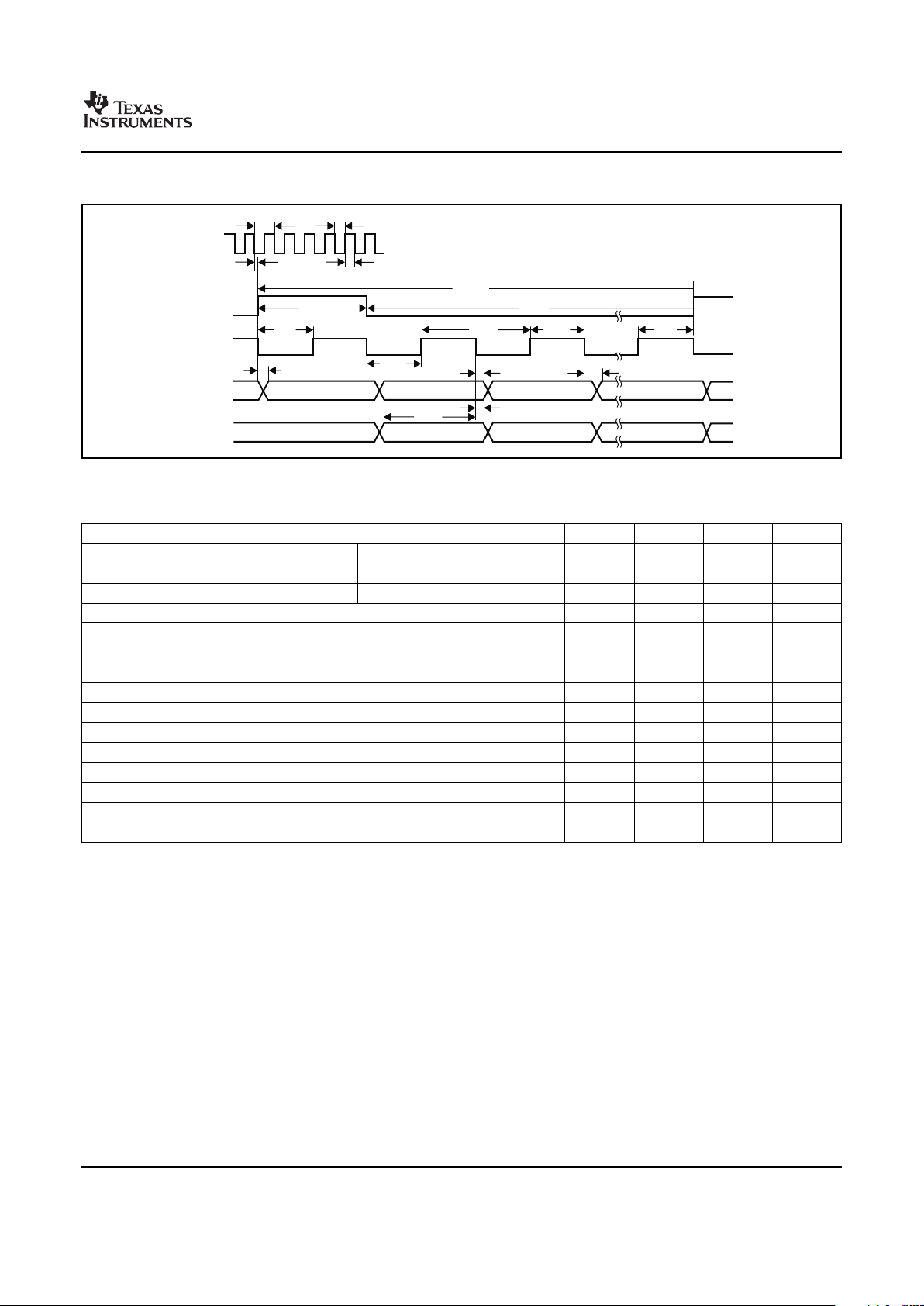
SCLK
FSYNC
DOUT
DIN
t
DOHD
t
FPW
t
SCLK
t
SF
t
SPW
t
SPW
t
FRAME
t
FPW
t
FS
t
DIHD
t
MSBPD
t
DIST
Bit23(MSB) Bit22 Bit21
t
DOPD
CLK
t
CPW
t
CPW
t
CS
t
CLK
TIMING REQUIREMENTS: FRAME-SYNC FORMAT
ADS1274
ADS1278
SBAS367 – JUNE 2007
TIMING CHARACTERISTICS: FRAME-SYNC FORMAT
For TA= – 40 ° C to +105 ° C, IOVDD = 1.65V to 3.6V, and DVDD = 1.65V to 1.95V.
SYMBOL PARAMETER MIN TYP MAX UNIT
All modes 37 10,000 ns
t
CLK
CLK period (1/f
CLK
)
High-Speed mode only 30.5 ns
t
CPW
CLK positive or negative pulse width 12 ns
t
CS
Falling edge of CLK to falling edge of SCLK – 0.25 0.25 t
CLK
t
FRAME
Frame period (1/f
DATA
)
(1)
256 2560 t
CLK
t
FPW
FSYNC positive or negative pulse width 1 t
SCLK
t
FS
Rising edge of FSYNC to rising edge of SCLK 5 ns
t
SF
Rising edge of SCLK to rising edge of FSYNC 5 ns
t
SCLK
SCLK period
(2)
1 t
CLK
t
SPW
SCLK positive or negative pulse width 0.4 t
CLK
t
DOHD
(3) (4)
SCLK falling edge to old DOUT invalid (hold time) 10 ns
t
DOPD
(4)
SCLK falling edge to new DOUT valid (propagation delay) 31 ns
t
MSBPD
FSYNC rising edge to DOUT MSB valid (propagation delay) 31 ns
t
DIST
New DIN valid to falling edge of SCLK (setup time) 6 ns
t
DIHD
(3)
Old DIN valid to falling edge of SCLK (hold time) 6 ns
(1) Depends on MODE[1:0] and CLKDIV selection. See Table 6 (f
CLK
/f
DATA
).
(2) SCLK must be continuously running and limited to ratios of 1, 1/2, 1/4, and 1/8 of f
CLK
.
(3) t
DOHD
(DOUT hold time) and t
DIHD
(DIN hold time) are specified under opposite worst-case conditions (digital supply voltage and
ambient temperature). Under equal conditions, with DOUT connected directly to DIN, the timing margin is >4ns.
(4) Load on DOUT = 20pF.
9
Copyright © 2007, Texas Instruments Incorporated
Submit Documentation Feedback
Product Folder Link(s): ADS1274 ADS1278
www.ti.com
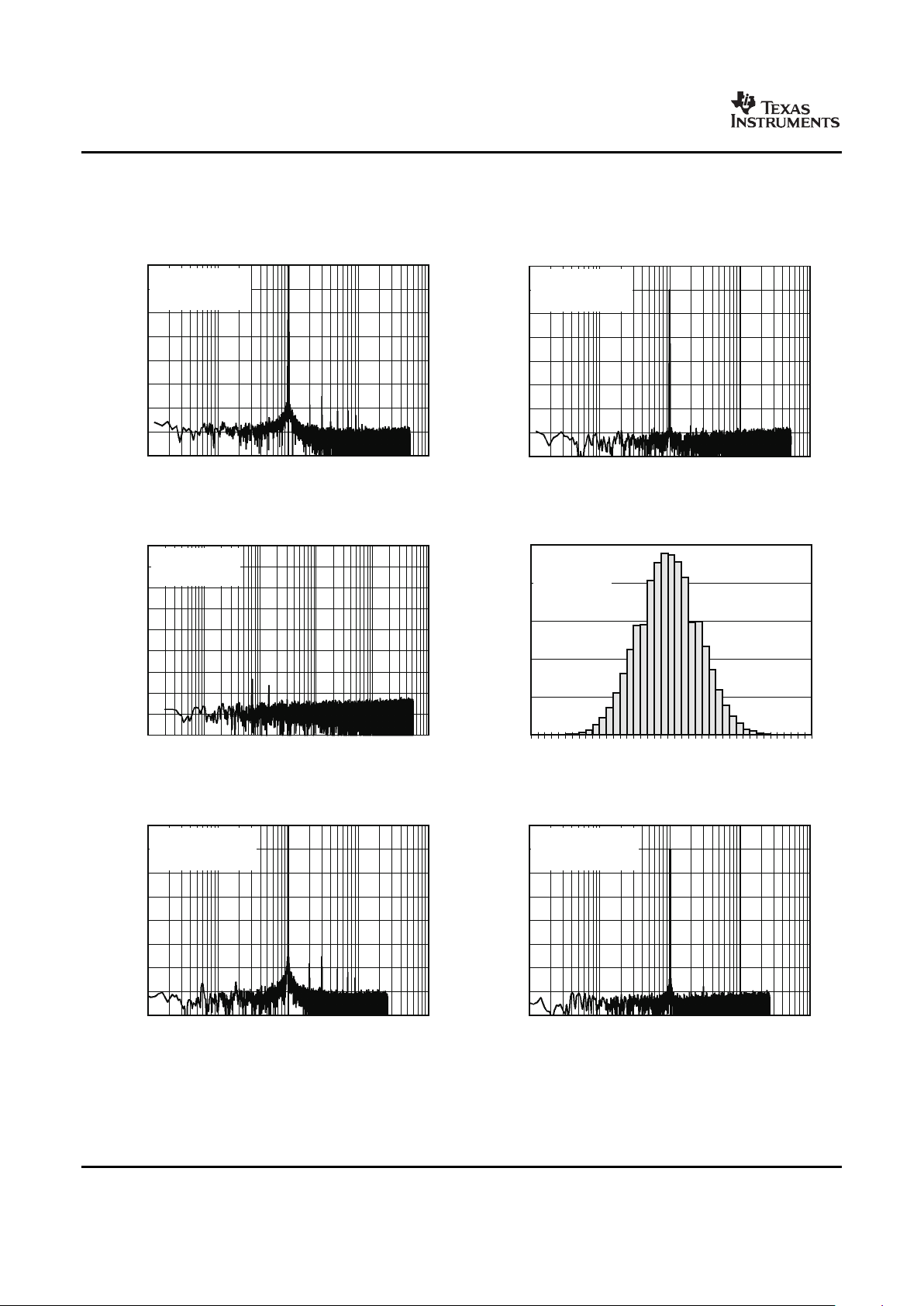
TYPICAL CHARACTERISTICS
10 100 1k
Frequency(Hz)
0
-20
-40
-60
-80
-100
-120
-140
-160
Amplitude(dB)
10k 100k
High-SpeedMode
f =1kHz, 0.5dBFS-
IN
32,768Points
10 100 1k
Frequency(Hz)
0
-20
-40
-60
-80
-100
-120
-140
-160
Amplitude(dB)
10k 100k
High-SpeedMode
f =1kHz, 20dBFS-
IN
32,768Points
1 10 100 1k
Frequency(Hz)
0
-20
-40
-60
-80
-100
-120
-140
-160
-180
Amplitude(dB)
10k 100k
High-SpeedMode
ShortedInput
262,144Points
-
35
-28
-21
-14
-7
0
7
14
21
28
35
Output( V)m
25k
20k
15k
10k
5k
0
NumberofOccurrences
High-SpeedMode
ShortedInput
262,144Points
10 100 1k
Frequency(Hz)
0
-20
-40
-60
-80
-100
-120
-140
-160
Amplitude(dB)
10k 100k
High-ResolutionMode
f =1kHz, 0.5dBFS-
IN
32,768Points
10 100 1k
Frequency(Hz)
0
-20
-40
-60
-80
-100
-120
-140
-160
Amplitude(dB)
10k 100k
High-ResolutionMode
f =1kHz, 20dBFS-
IN
32,768Points
ADS1274
ADS1278
SBAS367 – JUNE 2007
At TA= +25 ° C, High-Speed mode, AVDD = +5V, DVDD = +1.8V, IOVDD = +3.3V, f
CLK
= 27MHz, VREFP = 2.5V, and
VREFN = 0V, unless otherwise noted.
OUTPUT SPECTRUM OUTPUT SPECTRUM
Figure 1. Figure 2.
OUTPUT SPECTRUM NOISE HISTOGRAM
Figure 3. Figure 4.
OUTPUT SPECTRUM OUTPUT SPECTRUM
Figure 5. Figure 6.
10
Copyright © 2007, Texas Instruments Incorporated
Submit Documentation Feedback
Product Folder Link(s): ADS1274 ADS1278
www.ti.com
1 10 100 1k
Frequency(Hz)
0
-20
-40
-60
-80
-100
-120
-140
-160
-180
Amplitude(dB)
10k 100k
High-ResolutionMode
ShortedInput
262,144Points
-24.5
-
21.0
-
17.5
-14.0
-10.5
-7.0
-3.5
0
3.5
7.0
10.5
14.0
17.5
21.0
24.5
Output( V)m
25k
20k
15k
10k
5k
0
NumberofOccurrences
High-ResolutionMode
ShortedInput
262,144Points
10 100 1k
Frequency(Hz)
0
-20
-40
-60
-80
-100
-120
-140
-160
Amplitude(dB)
10k 100k
Low-PowerMode
f =1kHz, 0.5dBFS-
IN
32,768Points
10 100 1k
Frequency(Hz)
0
-20
-40
-60
-80
-100
-120
-140
-160
Amplitude(dB)
10k 100k
Low-PowerMode
f =1kHz, 20dBFS-
IN
32,768Points
1 10 100 1k
Frequency(Hz)
0
-20
-40
-60
-80
-100
-120
-140
-160
-180
Amplitude(dB)
10k 100k
Low-PowerMode
ShortedInput
262,144Points
-37
-32
-
26
-
21
-16
-11
-5
0
5
11
16
21
26
32
37
Output( V)m
25k
20k
15k
10k
5k
0
NumberofOccurrences
Low-PowerMode
ShortedInput
262,144Points
ADS1274
ADS1278
SBAS367 – JUNE 2007
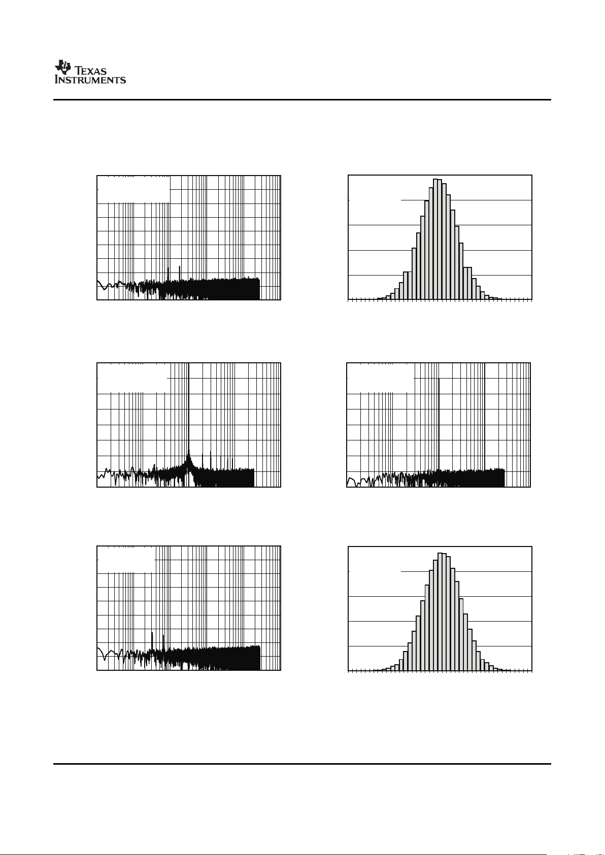
TYPICAL CHARACTERISTICS (continued)
At TA= +25 ° C, High-Speed mode, AVDD = +5V, DVDD = +1.8V, IOVDD = +3.3V, f
CLK
= 27MHz, VREFP = 2.5V, and
VREFN = 0V, unless otherwise noted.
OUTPUT SPECTRUM NOISE HISTOGRAM
Figure 7. Figure 8.
OUTPUT SPECTRUM OUTPUT SPECTRUM
Figure 9. Figure 10.
OUTPUT SPECTRUM NOISE HISTOGRAM
Figure 11. Figure 12.
11
Copyright © 2007, Texas Instruments Incorporated
Submit Documentation Feedback
Product Folder Link(s): ADS1274 ADS1278
www.ti.com
1 10 100
Frequency(Hz)
0
-20
-40
-60
-80
-100
-120
-140
-160
Amplitude(dB)
1k 10k
Low-SpeedMode
f =100Hz, 0.5dBFS-
IN
32,768Points
1 10 100
Frequency(Hz)
0
-20
-40
-60
-80
-100
-120
-140
-160
Amplitude(dB)
1k 10k
Low-SpeedMode
f =100Hz, 20dBFS-
IN
32,768Points
0.1 1 10 100
Frequency(Hz)
0
-20
-40
-60
-80
-100
-120
-140
-160
-180
Amplitude(dB)
1k 10k
Low-SpeedMode
ShortedInput
262,144Points
-35
-
28
-21
-14
-7
0
7
14
21
28
35
Output( V)m
25k
20k
15k
10k
5k
0
NumberofOccurrences
Low-SpeedMode
ShortedInput
262,144Points
10 100 1k
Frequency(Hz)
0
-20
-40
-60
-80
-100
-120
-140
THD,THD+N(dB)
10k 100k
High-SpeedMode
V = 0.5dBFS-
IN
THD+N
THD
-120 -100 -80 -60 -40
InputAmplitude(dBFS)
0
-20
-40
-60
-80
-100
-120
-140
THD,THD+N(dB)
-20 0
High-SpeedMode
f =1kHz
IN
THD+N
THD
ADS1274
ADS1278
SBAS367 – JUNE 2007
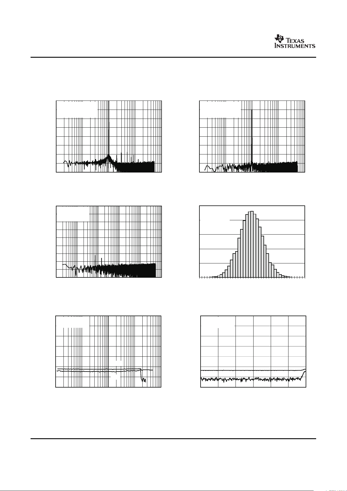
TYPICAL CHARACTERISTICS (continued)
At TA= +25 ° C, High-Speed mode, AVDD = +5V, DVDD = +1.8V, IOVDD = +3.3V, f
CLK
= 27MHz, VREFP = 2.5V, and
VREFN = 0V, unless otherwise noted.
OUTPUT SPECTRUM OUTPUT SPECTRUM
Figure 13. Figure 14.
OUTPUT SPECTRUM NOISE HISTOGRAM
Figure 15. Figure 16.
TOTAL HARMONIC DISTORTION TOTAL HARMONIC DISTORTION
vs FREQUENCY vs INPUT AMPLITUDE
Figure 17. Figure 18.
12
Copyright © 2007, Texas Instruments Incorporated
Submit Documentation Feedback
Product Folder Link(s): ADS1274 ADS1278
www.ti.com
10 100 1k
Frequency(Hz)
0
-20
-40
-60
-80
-100
-120
-140
THD,THD+N(dB)
10k 100k
High-ResolutionMode
V = 0.5dBFS-
IN
THD+N
THD
-120 -100 -80 -60 -40
InputAmplitude(dBFS)
0
-20
-40
-60
-80
-100
-120
-140
THD,THD+N(dB)
-20 0
High-ResolutionMode
f =1kHz
IN
THD+N
THD
10 100 1k
Frequency(Hz)
0
-20
-40
-60
-80
-100
-120
-140
THD,THD+N(dB)
10k 100k
Low-PowerMode
V = 0.5dBFS-
IN
THD+N
THD
-120 -100 -80 -60 -40
InputAmplitude(dBFS)
0
-20
-40
-60
-80
-100
-120
-140
THD,THD+N(dB)
-20 0
Low-PowerMode
f =1kHz
IN
THD+N
THD
10 100 1k
Frequency(Hz)
0
-20
-40
-60
-80
-100
-120
-140
THD,THD+N(dB)
10k
Low-SpeedMode
V = 0.5dBFS-
IN
THD+N
THD
-120 -100 -80 -60 -40
InputAmplitude(dBFS)
0
-20
-40
-60
-80
-100
-120
-140
THD,THD+N(dB)
-20 0
Low-SpeedMode
THD+N
THD
ADS1274
ADS1278
SBAS367 – JUNE 2007
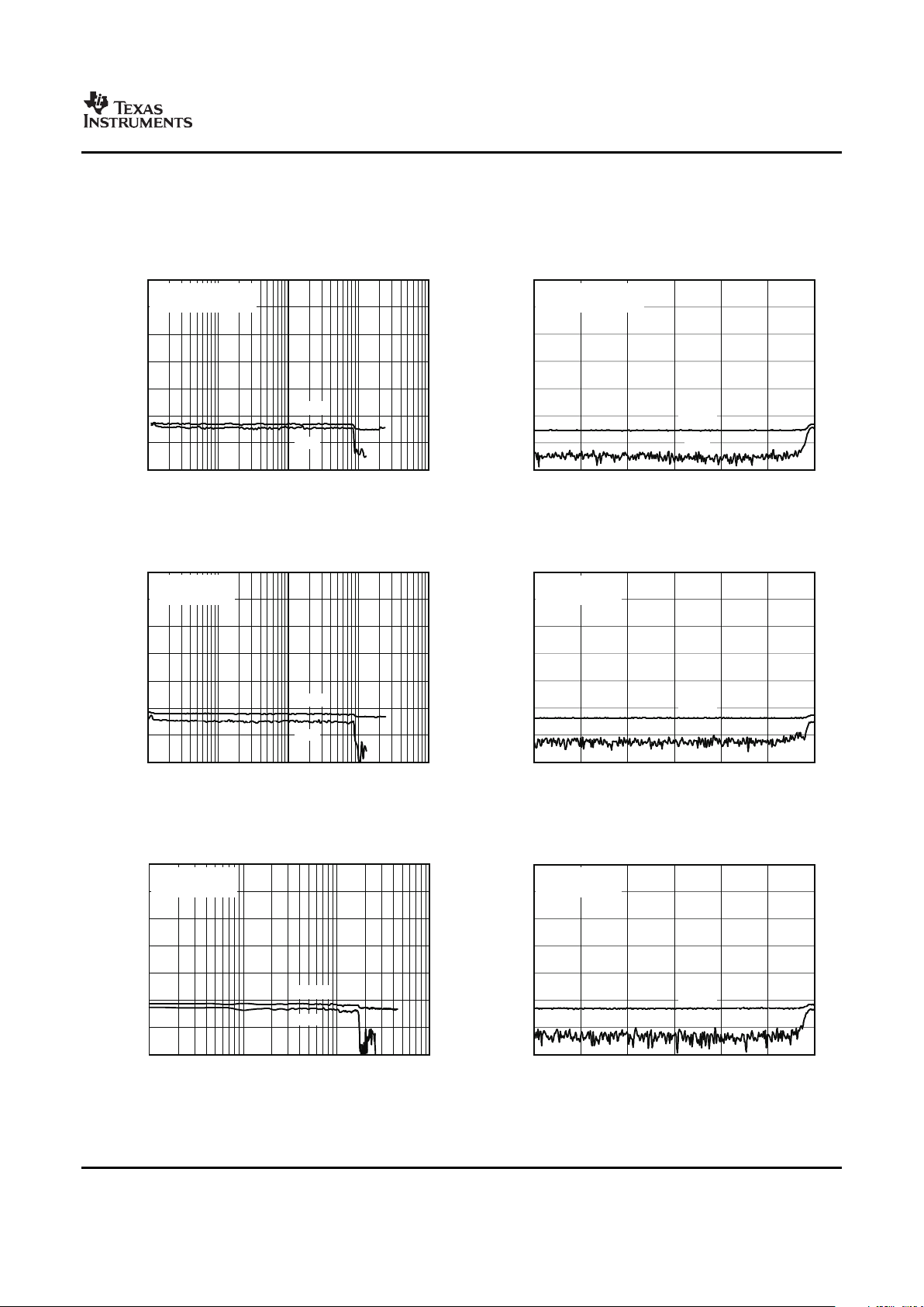
TYPICAL CHARACTERISTICS (continued)
At TA= +25 ° C, High-Speed mode, AVDD = +5V, DVDD = +1.8V, IOVDD = +3.3V, f
CLK
= 27MHz, VREFP = 2.5V, and
VREFN = 0V, unless otherwise noted.
TOTAL HARMONIC DISTORTION TOTAL HARMONIC DISTORTION
vs FREQUENCY vs INPUT AMPLITUDE
Figure 19. Figure 20.
TOTAL HARMONIC DISTORTION TOTAL HARMONIC DISTORTION
vs FREQUENCY vs INPUT AMPLITUDE
Figure 21. Figure 22.
TOTAL HARMONIC DISTORTION TOTAL HARMONIC DISTORTION
vs FREQUENCY vs INPUT AMPLITUDE
Figure 23. Figure 24.
13
Copyright © 2007, Texas Instruments Incorporated
Submit Documentation Feedback
Product Folder Link(s): ADS1274 ADS1278
www.ti.com
-10
-9
-8
-7
-
6
-5
-4
-3
-2
-1
0
1
2
3
4
5
6
7
8
9
10
OffsetDrift(mV/°C)
400
350
300
250
200
150
100
50
0
NumberofOccurrences
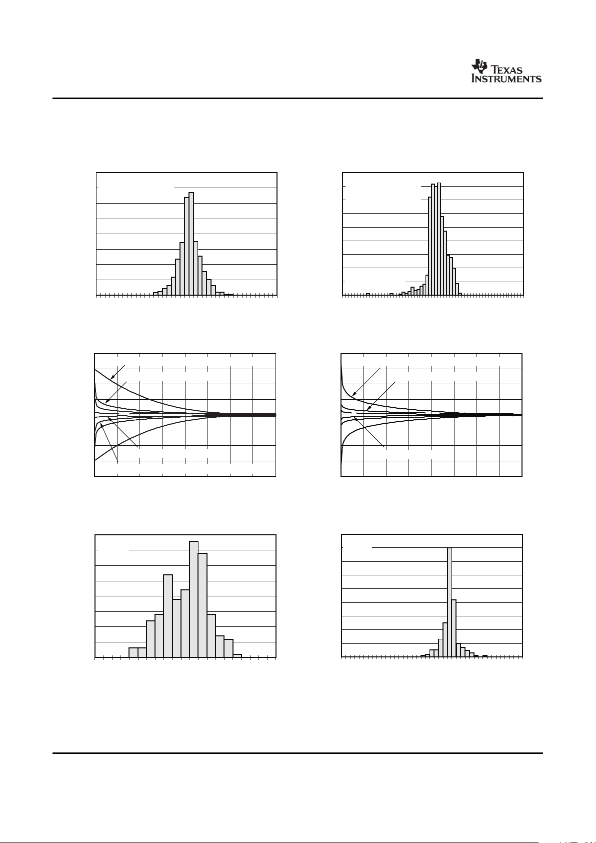
Multi-lotdatabasedon
20 Cintervalsoverthe°
range 40 Cto+105- ° °C.
-15
-14
-13
-12
-11
-10
-9
-8
-7
-6
-5
-4
-3
-2
-1
0
1
2
3
4
5
6
7
8
9
10
11
12
13
14
15
GainDrift(ppm/ C)°
900
800
700
600
500
400
300
200
100
0
NumberofOccurrences
25unitsbasedon
20 Cintervalsoverthe°
range 40 Cto+105- ° °C.
Outliers:T< 20 C°-
0 50 100 150 200 250 300 350
Time(s)
40
30
20
10
0
-10
-20
-30
-40
NormalizedOffset(
V)
m
400
ADS1278Low-SpeedMode
ADS1278High-SpeedandHigh-ResolutionModes
ADS1278Low-PowerMode
ADS1274High-SpeedandHigh-ResolutionModes
0 50 100 150 200 250 300 350
Time(s)
40
30
20
10
0
-10
-20
-30
-40
NormalizedGainError(ppm)
400
ADS1274/78High-SpeedandHigh-ResolutionModes
ADS1278Low-SpeedMode
ADS1278Low-PowerMode
-
1000
-900
-800
-
700
-600
-500
-400
-300
-200
-100
0
100
200
300
400
500
600
700
800
900
1000
Offset( V)m
40
35
30
25
20
15
10
5
0
NumberofOccurrences
High-SpeedMode
25Units
-4000
-3600
-3200
-
2800-2400
-2000
-1600
-1200
-800
-400
0
400
800
1200
1600
2000
2400
2800
3200
3600
4000
GainError(ppm)
90
80
70
60
50
40
30
20
10
0
NumberofOccurrences
High-SpeedMode
25Units
ADS1274
ADS1278
SBAS367 – JUNE 2007
TYPICAL CHARACTERISTICS (continued)
At TA= +25 ° C, High-Speed mode, AVDD = +5V, DVDD = +1.8V, IOVDD = +3.3V, f
CLK
= 27MHz, VREFP = 2.5V, and
VREFN = 0V, unless otherwise noted.
OFFSET DRIFT HISTOGRAM GAIN DRIFT HISTOGRAM
Figure 25. Figure 26.
OFFSET WARMUP DRIFT RESPONSE BAND GAIN WARMUP DRIFT RESPONSE BAND
Figure 27. Figure 28.
OFFSET ERROR HISTOGRAM GAIN ERROR HISTOGRAM
Figure 29. Figure 30.
14
Copyright © 2007, Texas Instruments Incorporated
Submit Documentation Feedback
Product Folder Link(s): ADS1274 ADS1278
www.ti.com
-1500
-1400
-1300
-1200
-1100
-1000
-
900
-
800
-
700
-
600
-
500
-
400
-
300
-
200
-
100
0
100
200
300
400
500
600
700
800
900
1000
1100
1200
1300
1400
1500
ChannelGainMatch(ppm)
100
90
80
70
60
50
40
30
20
10
0
NumberofOccurrences
High-SpeedMode
10Units
- 1500
- 1400
- 1300
- 1200
- 1100
- 1000
- 900
- 800
- 700
- 600
- 500
- 400
- 300
- 200
- 100
0
100
200
300
400
500
600
700
800
900
1000
1100
1200
1300
1400
1500
ChannelOffsetMatch( V)m
70
60
50
40
30
20
10
0
NumberofOccurrences
High-SpeedMode
10Units
-40 -20 0 20 40 60 80 100
Temperature( C)°
100
50
0
-50
-100
-150
-200
-250
-300
NormalizedOffset( V)m
300
250
200
150
100
50
0
-50
-100
NormalizedGainError(ppm)
120 125
Offset
Gain
2.40
2.41
2.42
2.43
2.44
2.45
2.46
2.47
2.48
2.49
2.50
2.51
2.52
2.53
2.54
2.55
2.56
2.57
2.58
2.59
2.60
VCOMVoltageOutput(V)
20
18
16
14
12
10
8
6
4
2
0
NumberofOccurrences
AVDD=5V
25Units,NoLoad
-40 -20 0 20 40 60 80 100
Temperature(°C)
1.36
1.34
1.32
1.30
1.28
1.26
1.24
1.22
ReferenceInputImpedance(k )W
13.6
13.4
13.2
13.0
12.8
12.6
12.4
12.2
ReferenceInputImpedance(k )W
120 125
High-Speedand
High-ResolutionModes
Low-SpeedMode
50
100
150
200
250
300
350
400
450
500
550
600
650
700
SamplingMatchError(ps)
40
35
30
25
20
15
10
5
0
NumberofOccurrences
30unitsover3productionlots,
inter-channelcombinations.
ADS1278
ADS1274
ADS1278
ADS1274
ADS1278
SBAS367 – JUNE 2007
TYPICAL CHARACTERISTICS (continued)
At TA= +25 ° C, High-Speed mode, AVDD = +5V, DVDD = +1.8V, IOVDD = +3.3V, f
CLK
= 27MHz, VREFP = 2.5V, and
VREFN = 0V, unless otherwise noted.
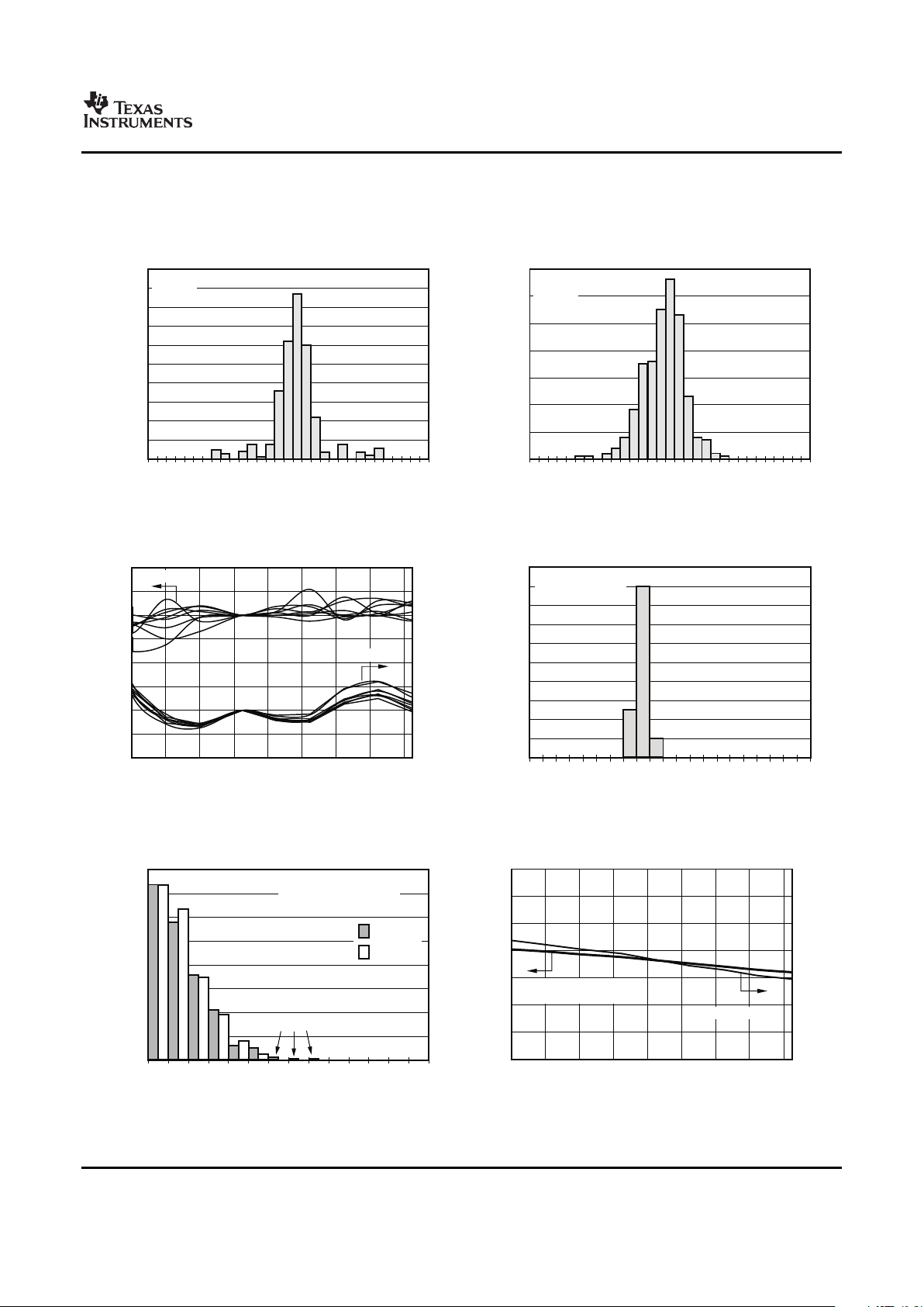
CHANNEL GAIN MATCH HISTOGRAM CHANNEL OFFSET MATCH HISTOGRAM
Figure 31. Figure 32.
OFFSET AND GAIN
vs TEMPERATURE VCOM VOLTAGE OUTPUT HISTOGRAM
Figure 33. Figure 34.
ADS1274/ADS1278 ADS1274 REFERENCE INPUT DIFFERENTIAL
SAMPLING MATCH ERROR HISTOGRAM IMPEDANCE vs TEMPERATURE
Figure 35. Figure 36.
15
Copyright © 2007, Texas Instruments Incorporated
Submit Documentation Feedback
Product Folder Link(s): ADS1274 ADS1278
 Loading...