


ADS1274
ADS1278
1
FEATURES
DESCRIPTION
APPLICATIONS
VREFP VREFN AVDD DVDD
TEST[1:0]
FORMAT[2:0]
CLK
SYNC
PWDN[8:1]
CLKDIV
Control
Logic
SPI
and
Frame-
Sync
Interface
IOVDD
DGNDAGND
DRDY/FSYNC
SCLK
DOUT[8:1]
DIN
Input2
Input1
Input4
Input3
Input6
Input5
Input8
Input7
DS
DS
DS
DS
DS
DS
DS
DS
PWDN[4:1]
ADS1278
Four
Digital
Filters
AVDD DVDD
TEST[1:0]
FORMAT[2:0]
CLK
SYNC
CLKDIV
Control
Logic
SPI
and
Frame-
Sync
Interface
IOVDD
DGNDAGND
DRDY/FSYNC
SCLK
DOUT[4:1]
DIN
ADS1274
MODE[1:0]
MODE[1:0]
Eight
Digital
Filters
VREFP VREFN
Input2
Input1
Input4
Input3
DS
DS
DS
DS
ADS1274
ADS1278
www.ti.com
SBAS367 – JUNE 2007
Quad/Octal, Simultaneous Sampling, 24-Bit Analog-to-Digital Converters
234
• Simultaneously Measure Four/Eight Channels
• Up to 128kSPS Data Rate
Based on the single-channel ADS1271 , the ADS1274
(quad) and ADS1278 (octal) are 24-bit, delta-sigma
• AC Performance:
( Δ Σ ) analog-to-digital converters (ADCs) with data
62kHz Bandwidth
rates up to 128k samples per second (SPS), allowing
111dB SNR (High-Resolution Mode)
simultaneous sampling of four or eight channels. The
– 108dB THD
devices are offered in identical packages, permitting
• DC Accuracy:
drop-in expandability.
0.8 μ V/ ° C Offset Drift
Traditionally, industrial delta-sigma ADCs offering
1.3ppm/ ° C Gain Drift
good drift performance use digital filters with large
• Selectable Operating Modes:
passband droop. As a result, they have limited signal
High-Speed: 128kSPS, 106dB SNR
bandwidth and are mostly suited for dc
High-Resolution: 52kSPS, 111dB SNR measurements. High-resolution ADCs in audio
applications offer larger usable bandwidths, but the
Low-Power: 52kSPS, 31mW/ch
offset and drift specifications are significantly weaker
Low-Speed: 10kSPS, 7mW/ch
than respective industrial counterparts. The ADS1274
• Linear Phase Digital Filter
and ADS1278 combine these types of converters,
• SPI™ or Frame-Sync Serial Interface
allowing high-precision industrial measurement with
excellent dc and ac specifications.
• Low Sampling Aperture Error
• Modulator Output Option (digital filter bypass)
The high-order, chopper-stabilized modulator
achieves very low drift with low in-band noise. The
• Analog Supply: 5V
onboard decimation filter suppresses modulator and
• Digital Core: 1.8V
signal out-of-band noise. These ADCs provide a
• I/O Supply: 1.8V to 3.3V
usable signal bandwidth up to 90% of the Nyquist
rate with less than 0.005dB of ripple.
Four operating modes allow for optimization of speed,
• Vibration/Modal Analysis
resolution, and power. All operations are controlled
• Multi-Channel Data Acquisition
directly by pins; there are no registers to program.
The devices are fully specified over the extended
• Acoustics/Dynamic Strain Gauges
industrial range ( – 40 ° C to +105 ° C) and are available
• Pressure Sensors
in an HTQFP-64 PowerPAD™ package.
1
Please be aware that an important notice concerning availability, standard warranty, and use in critical applications of
Texas Instruments semiconductor products and disclaimers thereto appears at the end of this data sheet.
2 PowerPAD is a trademark of Texas Instruments, Inc.
3 SPI is a trademark of Motorola, Inc.
4 All other trademarks are the property of their respective owners.
PRODUCTION DATA information is current as of publication date.
Copyright © 2007, Texas Instruments Incorporated
Products conform to specifications per the terms of the Texas
Instruments standard warranty. Production processing does not
necessarily include testing of all parameters.
www.ti.com
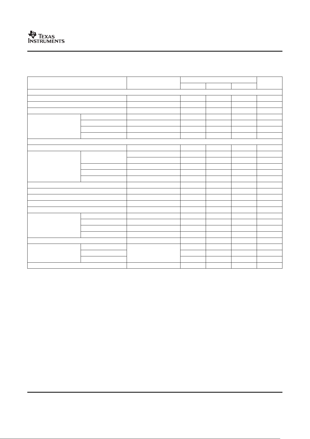
ABSOLUTE MAXIMUM RATINGS
ADS1274
ADS1278
SBAS367 – JUNE 2007
This integrated circuit can be damaged by ESD. Texas Instruments recommends that all integrated circuits be handled with
appropriate precautions. Failure to observe proper handling and installation procedures can cause damage.
ESD damage can range from subtle performance degradation to complete device failure. Precision integrated circuits may be more
susceptible to damage because very small parametric changes could cause the device not to meet its published specifications.
ORDERING INFORMATION
For the most current package and ordering information, see the Package Option Addendum at the end of this
document, or see the TI web site at www.ti.com .
Over operating free-air temperature range unless otherwise noted
(1)
ADS1274, ADS1278 UNIT
AVDD to AGND – 0.3 to +6.0 V
DVDD, IOVDD to DGND – 0.3 to +3.6 V
AGND to DGND – 0.3 to +0.3 V
Momentary 100 mA
Input current
Continuous 10 mA
Analog input to AGND – 0.3 to AVDD + 0.3 V
Digital input or output to DGND – 0.3 to DVDD + 0.3 V
Maximum junction temperature +150 ° C
ADS1274 – 40 to +125 ° C
Operating temperature range
ADS1278 – 40 to +105 ° C
Storage temperature range – 60 to +150 ° C
(1) Stresses above these ratings may cause permanent damage. Exposure to absolute maximum conditions for extended periods may
degrade device reliability. These are stress ratings only, and functional operation of the device at these or any other conditions beyond
those specified is not implied.
2
Copyright © 2007, Texas Instruments Incorporated
Submit Documentation Feedback
Product Folder Link(s): ADS1274 ADS1278
www.ti.com
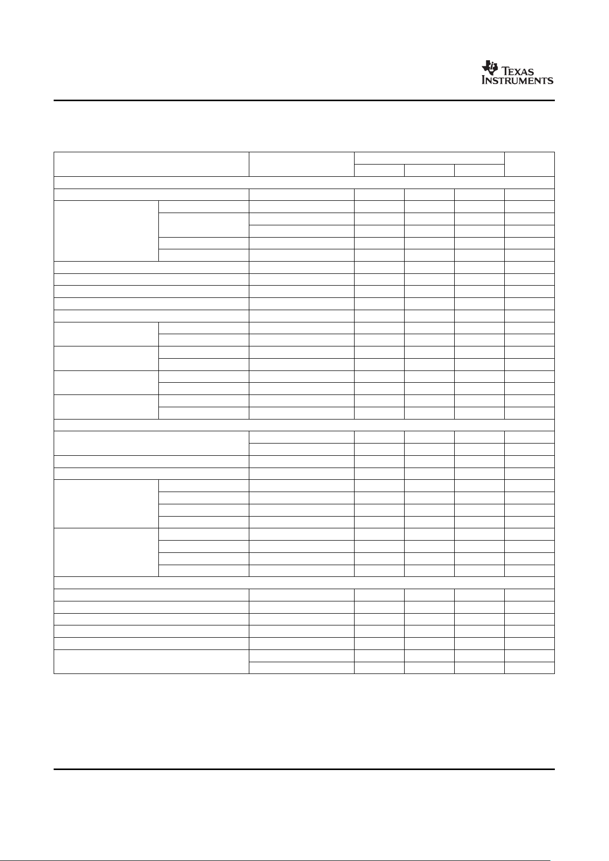
ELECTRICAL CHARACTERISTICS
ADS1274
ADS1278
SBAS367 – JUNE 2007
All specifications at TA= – 40 ° C to +105 ° C, AVDD = +5V, DVDD = +1.8V, IOVDD = +3.3V, f
CLK
= 27MHz, VREFP = 2.5V,
VREFN = 0V, and all channels active, unless otherwise noted.
ADS1274, ADS1278
PARAMETER TEST CONDITIONS MIN TYP MAX UNIT
Analog Inputs
Full-scale input voltage (FSR
(1)
) VIN= (AINP – AINN) ± V
REF
V
Absolute input voltage AINP or AINN to AGND AGND – 0.1 AVDD + 0.1 V
Common-mode input voltage (V
CM
) VCM= (AINP + AINN)/2 2.5 V
High-Speed mode 14 k Ω
High-Resolution mode 14 k Ω
Differential input impedance
Low-Power mode 28 k Ω
Low-Speed mode 140 k Ω
DC Performance
Resolution No missing codes 24 Bits
f
CLK
= 32.768MHz
(2)
128,000 SPS
High-Speed mode
f
CLK
= 27MHz 105,469 SPS
(3)
Data rate (f
DATA
) High-Resolution mode 52,734 SPS
Low-Power mode 52,734 SPS
Low-Speed mode 10,547 SPS
Integral nonlinearity (INL)
(4)
Differential input, VCM= 2.5V ± 0.0003 ± 0.0012 % FSR
(1)
Offset error 0.25 2 mV
Offset drift 0.8 μ V/ ° C
Gain error 0.1 0.5 % FSR
Gain drift 1.3 ppm/ ° C
High-Speed mode Shorted input 8.5 16 μ V, rms
High-Resolution mode Shorted input 5.5 12 μ V, rms
Noise
Low-Power mode Shorted input 8.5 16 μ V, rms
Low-Speed mode Shorted input 8.0 16 μ V, rms
Common-mode rejection fCM= 60Hz 90 108 dB
AVDD 80 dB
Power-supply rejection DVDD fPS= 60Hz 85 dB
IOVDD 105 dB
V
COM
output voltage No load AVDD/2 V
(1) FSR = full-scale range = 2V
REF
.
(2) f
CLK
= 32.768MHz max for High-Speed mode, and 27MHz max for all other modes. When f
CLK
> 27MHz, operation is limited to
Frame-Sync mode and V
REF
≤ 2.6V.
(3) SPS = samples per second.
(4) Best fit method.
3
Copyright © 2007, Texas Instruments Incorporated
Submit Documentation Feedback
Product Folder Link(s): ADS1274 ADS1278
www.ti.com
ADS1274
ADS1278
SBAS367 – JUNE 2007
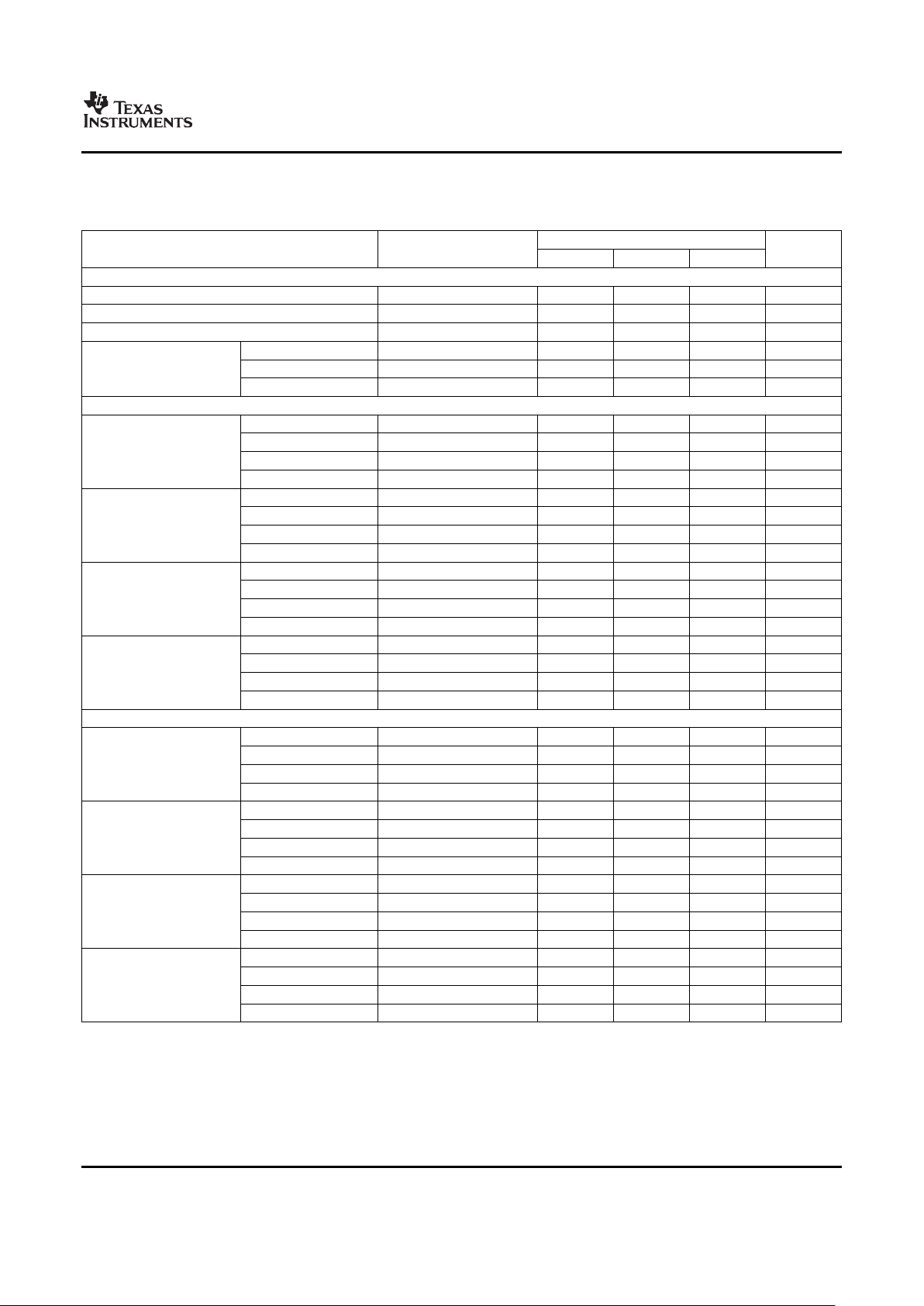
ELECTRICAL CHARACTERISTICS (continued)
All specifications at TA= – 40 ° C to +105 ° C, AVDD = +5V, DVDD = +1.8V, IOVDD = +3.3V, f
CLK
= 27MHz, VREFP = 2.5V,
VREFN = 0V, and all channels active, unless otherwise noted.
ADS1274, ADS1278
PARAMETER TEST CONDITIONS MIN TYP MAX UNIT
AC Performance
Crosstalk f = 1kHz, – 0.5dBFS
(5)
– 107 dB
High-Speed mode 101 106 dB
V
REF
= 2.5V 103 110 dB
High-Resolution mode
Signal-to-noise ratio (SNR)
(6)
V
REF
= 3V 111 dB
(unweighted)
Low-Power mode 101 106 dB
Low-Speed mode 101 107 dB
Total harmonic distortion (THD)
(7)
VIN= 1kHz, – 0.5dBFS – 108 – 96 dB
Spurious-free dynamic range 109 dB
Passband ripple ± 0.005 dB
Passband 0.453 f
DATA
Hz
– 3dB Bandwidth 0.49 f
DATA
Hz
High-Resolution mode 95 dB
Stop band attenuation
All other modes 100
High-Resolution mode 0.547 f
DATA
127.453 f
DATA
Hz
Stop band
All other modes 0.547 f
DATA
63.453 f
DATA
Hz
High-Resolution mode 39/f
DATA
s
Group delay
All other modes 38/f
DATA
s
High-Resolution mode Complete settling 78/f
DATA
s
Settling time (latency)
All other modes Complete settling 76/f
DATA
s
Voltage Reference Inputs
f
CLK
= 27MHz 0.5 2.5 3.1 V
Reference input voltage (V
REF
)
(V
REF
= VREFP – VREFN)
f
CLK
= 32.768MHz
(8)
0.5 2.5 2.6 V
Negative reference input (VREFN) AGND – 0.1 AGND + 0.1 V
Positive reference input (VREFP) VREFN + 0.5 AVDD + 0.1 V
High-Speed mode 1.3 k Ω
High-Resolution mode 1.3 k Ω
ADS1274
Reference Input impedance
Low-Power mode 2.6 k Ω
Low-Speed mode 13 k Ω
High-Speed mode 0.65 k Ω
High-Resolution mode 0.65 k Ω
ADS1278
Reference Input impedance
Low-Power mode 1.3 k Ω
Low-Speed mode 6.5 k Ω
Digital Input/Output (IOVDD = 1.8V to 3.6V)
V
IH
0.7 IOVDD IOVDD V
V
IL
DGND 0.3 IOVDD V
V
OH
IOH= 4mA 0.8 IOVDD IOVDD V
V
OL
IOL= 4mA DGND 0.2 IOVDD V
Input leakage 0 < V
IN DIGITAL
< IOVDD ± 10 μ A
High-Speed mode
(8)
0.1 32.768 MHz
Master clock rate (f
CLK
)
Other modes 0.1 27 MHz
(5) Worst-case channel crosstalk between one or more channels.
(6) Minimum SNR is ensured by the limit of the DC noise specification.
(7) THD includes the first nine harmonics of the input signal; Low-Speed mode includes the first five harmonics.
(8) f
CLK
= 32.768MHz max for High-Speed mode, and 27MHz max for all other modes. When f
CLK
> 27MHz, operation is limited to
Frame-Sync mode and V
REF
≤ 2.6V.
4
Copyright © 2007, Texas Instruments Incorporated
Submit Documentation Feedback
Product Folder Link(s): ADS1274 ADS1278
www.ti.com
ADS1274
ADS1278
SBAS367 – JUNE 2007
ELECTRICAL CHARACTERISTICS (continued)
All specifications at TA= – 40 ° C to +105 ° C, AVDD = +5V, DVDD = +1.8V, IOVDD = +3.3V, f
CLK
= 27MHz, VREFP = 2.5V,
VREFN = 0V, and all channels active, unless otherwise noted.
ADS1274, ADS1278
PARAMETER TEST CONDITIONS MIN TYP MAX UNIT
Power Supply
AVDD 4.75 5 5.25 V
DVDD 1.65 1.8 1.95 V
IOVDD 1.65 3.6 V
AVDD 1 10 μ A
Power-down current DVDD 1 15 μ A
IOVDD 1 10 μ A
ADS1274
High-Speed mode 50 75 mA
High-Resolution mode 50 75 mA
ADS1274
AVDD current
Low-Power mode 23 35 mA
Low-Speed mode 5 9 mA
High-Speed mode 18 24 mA
High-Resolution mode 12 17 mA
ADS1274
DVDD current
Low-Power mode 10 15 mA
Low-Speed mode 2.5 4.5 mA
High-Speed mode 0.15 0.5 mA
High-Resolution mode 0.075 0.3 mA
ADS1274
IOVDD current
Low-Power mode 0.075 0.3 mA
Low-Speed mode 0.02 0.15 mA
High-Speed mode 285 420 mW
High-Resolution mode 275 410 mW
ADS1274
Power dissipation
Low-Power mode 135 210 mW
Low-Speed mode 30 55 mW
ADS1278
High-Speed mode 97 145 mA
High-Resolution mode 97 145 mA
ADS1278
AVDD current
Low-Power mode 44 64 mA
Low-Speed mode 9 14 mA
High-Speed mode 23 30 mA
High-Resolution mode 16 20 mA
ADS1278
DVDD current
Low-Power mode 12 17 mA
Low-Speed mode 2.5 4.5 mA
High-Speed mode 0.25 1 mA
High-Resolution mode 0.125 0.5 mA
ADS1278
IOVDD current
Low-Power mode 0.125 0.5 mA
Low-Speed mode 0.035 0.2 mA
High-Speed mode 530 785 mW
High-Resolution mode 515 765 mW
ADS1278
Power dissipation
Low-Power mode 245 355 mW
Low-Speed mode 50 80 mW
5
Copyright © 2007, Texas Instruments Incorporated
Submit Documentation Feedback
Product Folder Link(s): ADS1274 ADS1278
www.ti.com
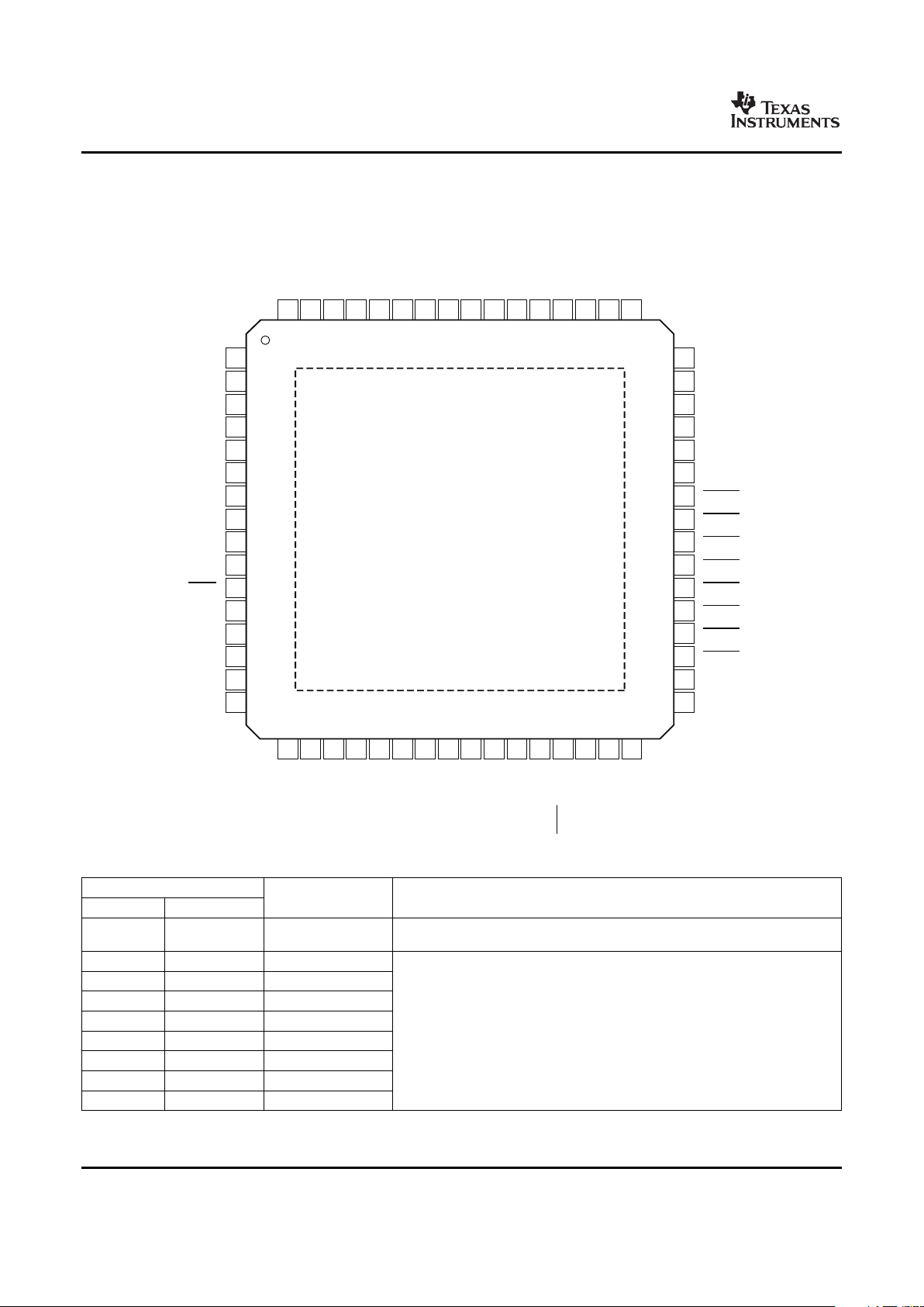
ADS1274/ADS1278 PIN ASSIGNMENTS
AINN7
(1)
AINP7
(1)
AINN8
(1)
AINP8
(1)
AVDD
AGND
PWDN1
PWDN2
PWDN3
PWDN4
PWDN5
(1)
PWDN6
(1)
PWDN7
(1)
PWDN8
(1)
MODE0
MODE1
AINP2
AINN2
AINP1
AINN1
AVDD
AGND
DGND
TEST0
TEST1
CLKDIV
SYNC
DIN
DOUT8
(1)
DOUT7
(1)
DOUT6
(1)
DOUT5
(1)
AINN3
AINP3
AINN4
AINP4
AVDD
AGND
VREFN
VREFP
VCOM
AGND
AVDD
AINP5
(1)
AINN6
(1)
AINP6
(1)
AINN5
(1)
DOUT4
DOUT3
DOUT2
DOUT1
DGND
IOVDD
IOVDD
DGND
DGND
DVDD
CLK
SCLK
DRDY
/FSYNC
FORMAT2
FORMAT1
FORMAT0
ADS1274/ADS1278
AGND
1
2
3
4
5
6
7
8
9
10
11
12
13
14
15
16
48
47
46
45
44
43
42
41
40
39
38
37
36
35
34
33
17
18
19
20
21
22
23
24
25
26
27
28
29
30
31
32
64
63
62
61
60
59
58
57
56
55
54
53
52
51
50
49
(PowerPADOutline)
NOTE:(1) pinnamesindicateadditionalpinsforBoldface
theADS1278;seepindescriptions.
ADS1274
ADS1278
SBAS367 – JUNE 2007
PAP PACKAGE
HTQFP-64
(TOP VIEW)
ADS1274/ADS1278 PIN DESCRIPTIONS
PIN
NAME NO. FUNCTION DESCRIPTION
6, 43, 54,
AGND Analog ground Analog ground; connect to DGND using a single plane.
58, 59
AINP1 3 Analog input
AINP2 1 Analog input
AINP3 63 Analog input ADS1278: AINP[8:1] Positive analog input, channels 8 through 1.
AINP4 61 Analog input
AINP5 51 Analog input ADS1274: AINP[8:5] Connected to internal ESD rails. The inputs may float.
AINP[4:1] Positive analog input, channels 4 through 1.
AINP6 49 Analog input
AINP7 47 Analog input
AINP8 45 Analog input
6
Copyright © 2007, Texas Instruments Incorporated
Submit Documentation Feedback
Product Folder Link(s): ADS1274 ADS1278
www.ti.com
ADS1274
ADS1278
SBAS367 – JUNE 2007
ADS1274/ADS1278 PIN DESCRIPTIONS (continued)
PIN
NAME NO. FUNCTION DESCRIPTION
AINN1 4 Analog input
AINN2 2 Analog input
AINN3 64 Analog input ADS1278: AINN[8:1] Negative analog input, channels 8 through 1.
AINN4 62 Analog input
AINN5 52 Analog input ADS1274: AINN[8:5] Connected to internal ESD rails. The inputs may float.
AINN[4:1] Negative analog input, channels 4 through 1.
AINN6 50 Analog input
AINN7 48 Analog input
AINN8 46 Analog input
AVDD 5, 44, 53, 60 Analog power supply Analog power supply (4.75V to 5.25V).
VCOM 55 Analog output AVDD/2 Unbuffered voltage output.
VREFN 57 Analog input Negative reference input.
VREFP 56 Analog input Positive reference input.
CLK 27 Digital input Master clock input.
CLK input divider control: 1 = 32.768MHz (High-Speed mode only) / 27MHz
CLKDIV 10 Digital input
0 = 13.5MHz (low-power) / 5.4MHz (low-speed)
DGND 7, 21, 24, 25 Digital ground Digital ground power supply.
DIN 12 Digital input Daisy-chain data input.
DOUT1 20 Digital output DOUT1 is TDM data output (TDM mode).
DOUT2 19 Digital output
DOUT3 18 Digital output ADS1278: DOUT[8:1] Data output for channels 8 through 1.
DOUT4 17 Digital output
DOUT5 16 Digital output ADS1274: DOUT[8:5] Internally connected to active circuitry; outputs are
driven.
DOUT6 15 Digital output
DOUT[4:1] Data output for channels 4 through 1.
DOUT7 14 Digital output
DOUT8 13 Digital output
DRDY/
29 Digital input/output Frame-Sync protocol: frame clock input; SPI protocol: data ready output.
FSYNC
DVDD 26 Digital power supply Digital core power supply (+1.65V to +1.95V).
FORMAT0 32 Digital input
FORMAT[2:0] Selects Frame-Sync/SPI protocol, TDM/discrete data outputs,
FORMAT1 31 Digital input
fixed/dynamic position TDM data, and modulator mode/normal operating mode.
FORMAT2 30 Digital input
IOVDD 22, 23 Digital power supply I/O power supply (+1.65V to +3.6V).
MODE0 34 Digital input
MODE[1:0] Selects High-Speed, High-Resolution, Low-Power, or Low-Speed
mode operation.
MODE1 33 Digital input
PWDN1 42 Digital input
PWDN2 41 Digital input
PWDN3 40 Digital input ADS1278: PWDN[8:1] Power-down control for channels 8 through 1.
PWDN4 39 Digital input
PWDN5 38 Digital input ADS1274: PWDN[8:5] must = 0V.
PWDN[4:1] Power-down control for channels 4 through 1.
PWDN6 37 Digital input
PWDN7 36 Digital input
PWDN8 35 Digital input
SCLK 28 Digital input/output Serial clock input, Modulator clock output.
SYNC 11 Digital input Synchronize input (all channels).
TEST0 8 Digital input TEST[1:0] Test mode select: 00 = Normal operation 01 = Do not use
11 = Boundary scan test 10 = Do not use
TEST1 9 Digital input
mode
7
Copyright © 2007, Texas Instruments Incorporated
Submit Documentation Feedback
Product Folder Link(s): ADS1274 ADS1278
www.ti.com
CLK
t
CPW
t
CLK
t
CPW
t
SD
t
SCLK
t
DIST
t
DOHD
t
SPW
Bit23(MSB) Bit22 Bit21
t
SPW
t
DOPD
t
CD
t
DS
t
MSBPD
t
DIHD
· · ·
t
CONV
DRDY
SCLK
DOUT
DIN
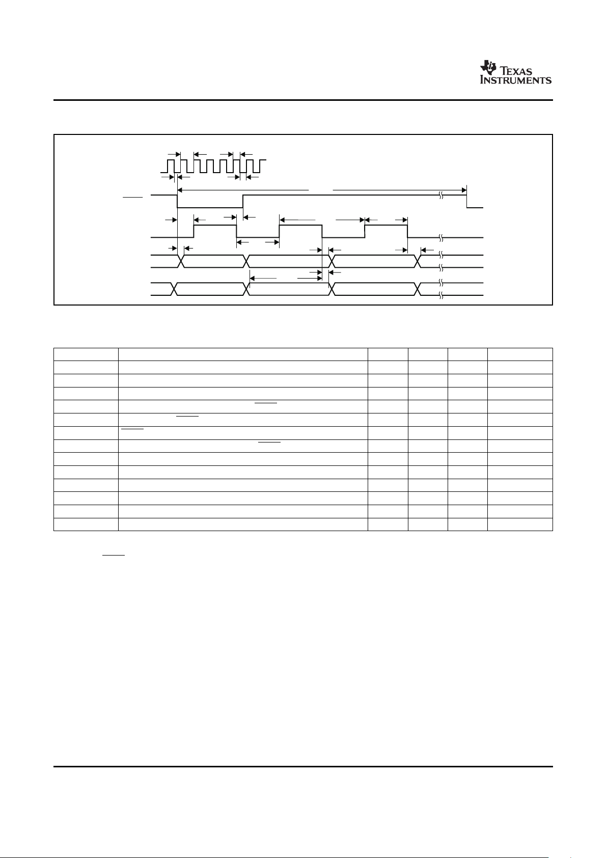
TIMING REQUIREMENTS: SPI FORMAT
ADS1274
ADS1278
SBAS367 – JUNE 2007
TIMING CHARACTERISTICS: SPI FORMAT
For TA= – 40 ° C to +105 ° C, IOVDD = 1.65V to 3.6V, and DVDD = 1.65V to 1.95V.
SYMBOL PARAMETER MIN TYP MAX UNIT
t
CLK
CLK period (1/f
CLK
)
(1)
37 10,000 ns
t
CPW
CLK positive or negative pulse width 15 ns
t
CONV
Conversion period (1/f
DATA
)
(2)
256 2560 t
CLK
t
CD
(3)
Falling edge of CLK to falling edge of DRDY 22 ns
t
DS
(3)
Falling edge of DRDY to rising edge of first SCLK to retrieve data 1 t
CLK
t
MSBPD
DRDY falling edge to DOUT MSB valid (propagation delay) 16 ns
t
SD
(3)
Falling edge of SCLK to rising edge of DRDY 18 ns
t
SCLK
(4)
SCLK period 1 t
CLK
t
SPW
SCLK positive or negative pulse width 0.4 t
CLK
t
DOHD
(3) (5)
SCLK falling edge to new DOUT invalid (hold time) 10 ns
t
DOPD
(3)
SCLK falling edge to new DOUT valid (propagation delay) 32 ns
t
DIST
New DIN valid to falling edge of SCLK (setup time) 6 ns
t
DIHD
(5)
Old DIN valid to falling edge of SCLK (hold time) 6 ns
(1) f
CLK
= 27MHz maximum.
(2) Depends on MODE[1:0] and CLKDIV selection. See Table 6 (f
CLK
/f
DATA
).
(3) Load on DRDY and DOUT = 20pF.
(4) For best performance, limit f
SCLK
/f
CLK
to ratios of 1, 1/2, 1/4, 1/8, etc.
(5) t
DOHD
(DOUT hold time) and t
DIHD
(DIN hold time) are specified under opposite worst-case conditions (digital supply voltage and
ambient temperature). Under equal conditions, with DOUT connected directly to DIN, the timing margin is >4ns.
8
Copyright © 2007, Texas Instruments Incorporated
Submit Documentation Feedback
Product Folder Link(s): ADS1274 ADS1278
www.ti.com
SCLK
FSYNC
DOUT
DIN
t
DOHD
t
FPW
t
SCLK
t
SF
t
SPW
t
SPW
t
FRAME
t
FPW
t
FS
t
DIHD
t
MSBPD
t
DIST
Bit23(MSB) Bit22 Bit21
t
DOPD
CLK
t
CPW
t
CPW
t
CS
t
CLK
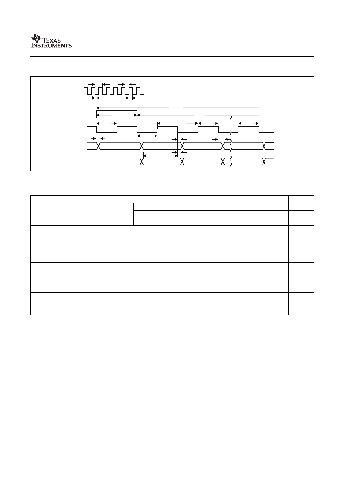
TIMING REQUIREMENTS: FRAME-SYNC FORMAT
ADS1274
ADS1278
SBAS367 – JUNE 2007
TIMING CHARACTERISTICS: FRAME-SYNC FORMAT
For TA= – 40 ° C to +105 ° C, IOVDD = 1.65V to 3.6V, and DVDD = 1.65V to 1.95V.
SYMBOL PARAMETER MIN TYP MAX UNIT
All modes 37 10,000 ns
t
CLK
CLK period (1/f
CLK
)
High-Speed mode only 30.5 ns
t
CPW
CLK positive or negative pulse width 12 ns
t
CS
Falling edge of CLK to falling edge of SCLK – 0.25 0.25 t
CLK
t
FRAME
Frame period (1/f
DATA
)
(1)
256 2560 t
CLK
t
FPW
FSYNC positive or negative pulse width 1 t
SCLK
t
FS
Rising edge of FSYNC to rising edge of SCLK 5 ns
t
SF
Rising edge of SCLK to rising edge of FSYNC 5 ns
t
SCLK
SCLK period
(2)
1 t
CLK
t
SPW
SCLK positive or negative pulse width 0.4 t
CLK
t
DOHD
(3) (4)
SCLK falling edge to old DOUT invalid (hold time) 10 ns
t
DOPD
(4)
SCLK falling edge to new DOUT valid (propagation delay) 31 ns
t
MSBPD
FSYNC rising edge to DOUT MSB valid (propagation delay) 31 ns
t
DIST
New DIN valid to falling edge of SCLK (setup time) 6 ns
t
DIHD
(3)
Old DIN valid to falling edge of SCLK (hold time) 6 ns
(1) Depends on MODE[1:0] and CLKDIV selection. See Table 6 (f
CLK
/f
DATA
).
(2) SCLK must be continuously running and limited to ratios of 1, 1/2, 1/4, and 1/8 of f
CLK
.
(3) t
DOHD
(DOUT hold time) and t
DIHD
(DIN hold time) are specified under opposite worst-case conditions (digital supply voltage and
ambient temperature). Under equal conditions, with DOUT connected directly to DIN, the timing margin is >4ns.
(4) Load on DOUT = 20pF.
9
Copyright © 2007, Texas Instruments Incorporated
Submit Documentation Feedback
Product Folder Link(s): ADS1274 ADS1278
www.ti.com
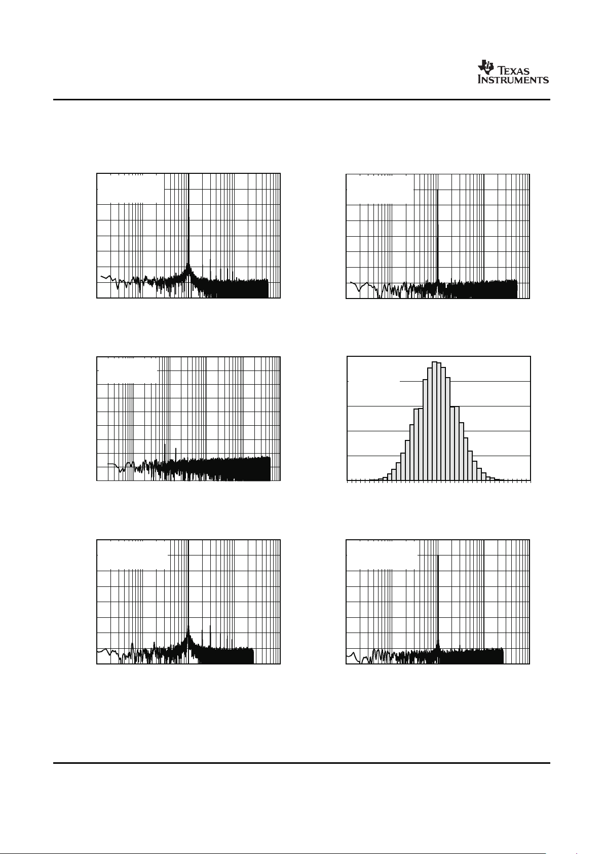
TYPICAL CHARACTERISTICS
10 100 1k
Frequency(Hz)
0
-20
-40
-60
-80
-100
-120
-140
-160
Amplitude(dB)
10k 100k
High-SpeedMode
f =1kHz, 0.5dBFS-
IN
32,768Points
10 100 1k
Frequency(Hz)
0
-20
-40
-60
-80
-100
-120
-140
-160
Amplitude(dB)
10k 100k
High-SpeedMode
f =1kHz, 20dBFS-
IN
32,768Points
1 10 100 1k
Frequency(Hz)
0
-20
-40
-60
-80
-100
-120
-140
-160
-180
Amplitude(dB)
10k 100k
High-SpeedMode
ShortedInput
262,144Points
-
35
-28
-21
-14
-7
0
7
14
21
28
35
Output( V)m
25k
20k
15k
10k
5k
0
NumberofOccurrences
High-SpeedMode
ShortedInput
262,144Points
10 100 1k
Frequency(Hz)
0
-20
-40
-60
-80
-100
-120
-140
-160
Amplitude(dB)
10k 100k
High-ResolutionMode
f =1kHz, 0.5dBFS-
IN
32,768Points
10 100 1k
Frequency(Hz)
0
-20
-40
-60
-80
-100
-120
-140
-160
Amplitude(dB)
10k 100k
High-ResolutionMode
f =1kHz, 20dBFS-
IN
32,768Points
ADS1274
ADS1278
SBAS367 – JUNE 2007
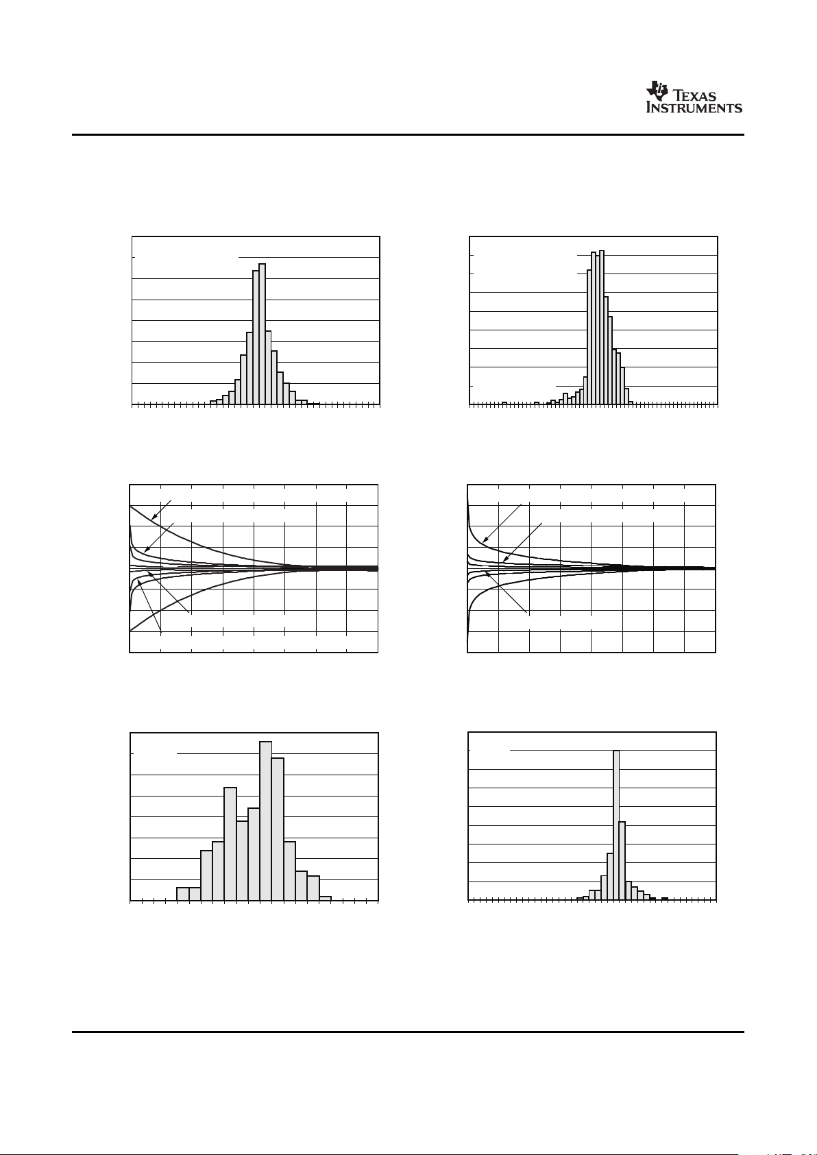
At TA= +25 ° C, High-Speed mode, AVDD = +5V, DVDD = +1.8V, IOVDD = +3.3V, f
CLK
= 27MHz, VREFP = 2.5V, and
VREFN = 0V, unless otherwise noted.
OUTPUT SPECTRUM OUTPUT SPECTRUM
Figure 1. Figure 2.
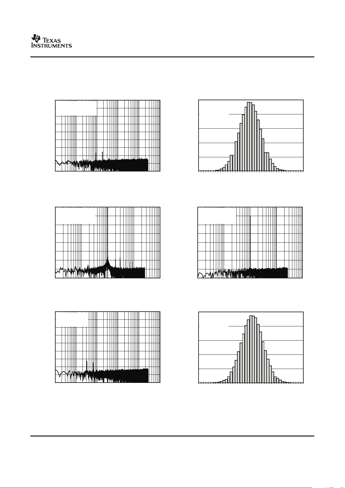
OUTPUT SPECTRUM NOISE HISTOGRAM
Figure 3. Figure 4.
OUTPUT SPECTRUM OUTPUT SPECTRUM
Figure 5. Figure 6.
10
Copyright © 2007, Texas Instruments Incorporated
Submit Documentation Feedback
Product Folder Link(s): ADS1274 ADS1278
www.ti.com
1 10 100 1k
Frequency(Hz)
0
-20
-40
-60
-80
-100
-120
-140
-160
-180
Amplitude(dB)
10k 100k
High-ResolutionMode
ShortedInput
262,144Points
-24.5
-
21.0
-
17.5
-14.0
-10.5
-7.0
-3.5
0
3.5
7.0
10.5
14.0
17.5
21.0
24.5
Output( V)m
25k
20k
15k
10k
5k
0
NumberofOccurrences
High-ResolutionMode
ShortedInput
262,144Points
10 100 1k
Frequency(Hz)
0
-20
-40
-60
-80
-100
-120
-140
-160
Amplitude(dB)
10k 100k
Low-PowerMode
f =1kHz, 0.5dBFS-
IN
32,768Points
10 100 1k
Frequency(Hz)
0
-20
-40
-60
-80
-100
-120
-140
-160
Amplitude(dB)
10k 100k
Low-PowerMode
f =1kHz, 20dBFS-
IN
32,768Points
1 10 100 1k
Frequency(Hz)
0
-20
-40
-60
-80
-100
-120
-140
-160
-180
Amplitude(dB)
10k 100k
Low-PowerMode
ShortedInput
262,144Points
-37
-32
-
26
-
21
-16
-11
-5
0
5
11
16
21
26
32
37
Output( V)m
25k
20k
15k
10k
5k
0
NumberofOccurrences
Low-PowerMode
ShortedInput
262,144Points
ADS1274
ADS1278
SBAS367 – JUNE 2007
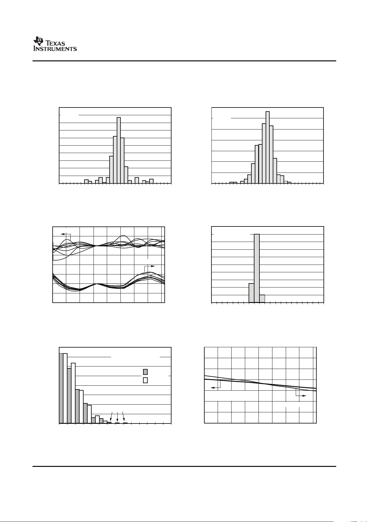
TYPICAL CHARACTERISTICS (continued)
At TA= +25 ° C, High-Speed mode, AVDD = +5V, DVDD = +1.8V, IOVDD = +3.3V, f
CLK
= 27MHz, VREFP = 2.5V, and
VREFN = 0V, unless otherwise noted.
OUTPUT SPECTRUM NOISE HISTOGRAM
Figure 7. Figure 8.
OUTPUT SPECTRUM OUTPUT SPECTRUM
Figure 9. Figure 10.
OUTPUT SPECTRUM NOISE HISTOGRAM
Figure 11. Figure 12.
11
Copyright © 2007, Texas Instruments Incorporated
Submit Documentation Feedback
Product Folder Link(s): ADS1274 ADS1278
www.ti.com
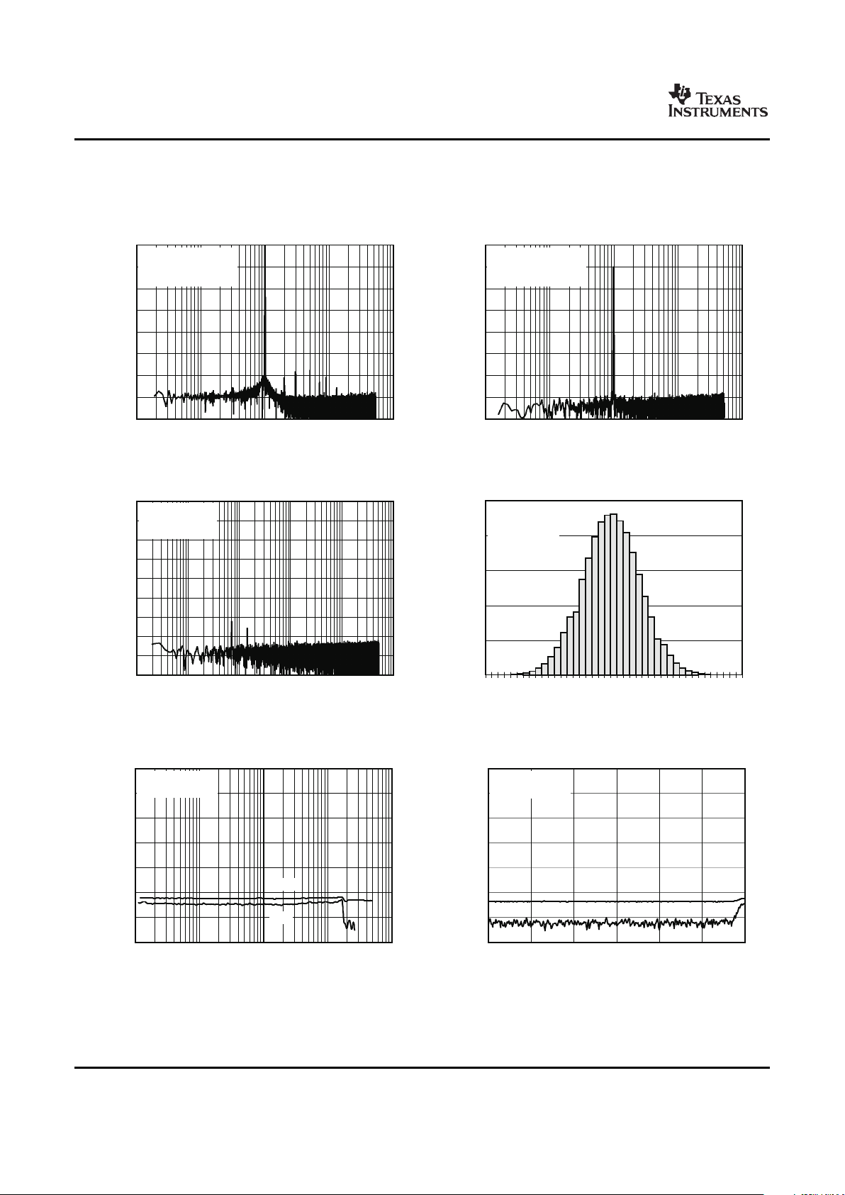
1 10 100
Frequency(Hz)
0
-20
-40
-60
-80
-100
-120
-140
-160
Amplitude(dB)
1k 10k
Low-SpeedMode
f =100Hz, 0.5dBFS-
IN
32,768Points
1 10 100
Frequency(Hz)
0
-20
-40
-60
-80
-100
-120
-140
-160
Amplitude(dB)
1k 10k
Low-SpeedMode
f =100Hz, 20dBFS-
IN
32,768Points
0.1 1 10 100
Frequency(Hz)
0
-20
-40
-60
-80
-100
-120
-140
-160
-180
Amplitude(dB)
1k 10k
Low-SpeedMode
ShortedInput
262,144Points
-35
-
28
-21
-14
-7
0
7
14
21
28
35
Output( V)m
25k
20k
15k
10k
5k
0
NumberofOccurrences
Low-SpeedMode
ShortedInput
262,144Points
10 100 1k
Frequency(Hz)
0
-20
-40
-60
-80
-100
-120
-140
THD,THD+N(dB)
10k 100k
High-SpeedMode
V = 0.5dBFS-
IN
THD+N
THD
-120 -100 -80 -60 -40
InputAmplitude(dBFS)
0
-20
-40
-60
-80
-100
-120
-140
THD,THD+N(dB)
-20 0
High-SpeedMode
f =1kHz
IN
THD+N
THD
ADS1274
ADS1278
SBAS367 – JUNE 2007
TYPICAL CHARACTERISTICS (continued)
At TA= +25 ° C, High-Speed mode, AVDD = +5V, DVDD = +1.8V, IOVDD = +3.3V, f
CLK
= 27MHz, VREFP = 2.5V, and
VREFN = 0V, unless otherwise noted.
OUTPUT SPECTRUM OUTPUT SPECTRUM
Figure 13. Figure 14.
OUTPUT SPECTRUM NOISE HISTOGRAM
Figure 15. Figure 16.
TOTAL HARMONIC DISTORTION TOTAL HARMONIC DISTORTION
vs FREQUENCY vs INPUT AMPLITUDE
Figure 17. Figure 18.
12
Copyright © 2007, Texas Instruments Incorporated
Submit Documentation Feedback
Product Folder Link(s): ADS1274 ADS1278
www.ti.com
10 100 1k
Frequency(Hz)
0
-20
-40
-60
-80
-100
-120
-140
THD,THD+N(dB)
10k 100k
High-ResolutionMode
V = 0.5dBFS-
IN
THD+N
THD
-120 -100 -80 -60 -40
InputAmplitude(dBFS)
0
-20
-40
-60
-80
-100
-120
-140
THD,THD+N(dB)
-20 0
High-ResolutionMode
f =1kHz
IN
THD+N
THD
10 100 1k
Frequency(Hz)
0
-20
-40
-60
-80
-100
-120
-140
THD,THD+N(dB)
10k 100k
Low-PowerMode
V = 0.5dBFS-
IN
THD+N
THD
-120 -100 -80 -60 -40
InputAmplitude(dBFS)
0
-20
-40
-60
-80
-100
-120
-140
THD,THD+N(dB)
-20 0
Low-PowerMode
f =1kHz
IN
THD+N
THD
10 100 1k
Frequency(Hz)
0
-20
-40
-60
-80
-100
-120
-140
THD,THD+N(dB)
10k
Low-SpeedMode
V = 0.5dBFS-
IN
THD+N
THD
-120 -100 -80 -60 -40
InputAmplitude(dBFS)
0
-20
-40
-60
-80
-100
-120
-140
THD,THD+N(dB)
-20 0
Low-SpeedMode
THD+N
THD
ADS1274
ADS1278
SBAS367 – JUNE 2007
TYPICAL CHARACTERISTICS (continued)
At TA= +25 ° C, High-Speed mode, AVDD = +5V, DVDD = +1.8V, IOVDD = +3.3V, f
CLK
= 27MHz, VREFP = 2.5V, and
VREFN = 0V, unless otherwise noted.
TOTAL HARMONIC DISTORTION TOTAL HARMONIC DISTORTION
vs FREQUENCY vs INPUT AMPLITUDE
Figure 19. Figure 20.
TOTAL HARMONIC DISTORTION TOTAL HARMONIC DISTORTION
vs FREQUENCY vs INPUT AMPLITUDE
Figure 21. Figure 22.
TOTAL HARMONIC DISTORTION TOTAL HARMONIC DISTORTION
vs FREQUENCY vs INPUT AMPLITUDE
Figure 23. Figure 24.
13
Copyright © 2007, Texas Instruments Incorporated
Submit Documentation Feedback
Product Folder Link(s): ADS1274 ADS1278
www.ti.com
-10
-9
-8
-7
-
6
-5
-4
-3
-2
-1
0
1
2
3
4
5
6
7
8
9
10
OffsetDrift(mV/°C)
400
350
300
250
200
150
100
50
0
NumberofOccurrences
Multi-lotdatabasedon
20 Cintervalsoverthe°
range 40 Cto+105- ° °C.
-15
-14
-13
-12
-11
-10
-9
-8
-7
-6
-5
-4
-3
-2
-1
0
1
2
3
4
5
6
7
8
9
10
11
12
13
14
15
GainDrift(ppm/ C)°
900
800
700
600
500
400
300
200
100
0
NumberofOccurrences
25unitsbasedon
20 Cintervalsoverthe°
range 40 Cto+105- ° °C.
Outliers:T< 20 C°-
0 50 100 150 200 250 300 350
Time(s)
40
30
20
10
0
-10
-20
-30
-40
NormalizedOffset(
V)
m
400
ADS1278Low-SpeedMode
ADS1278High-SpeedandHigh-ResolutionModes
ADS1278Low-PowerMode
ADS1274High-SpeedandHigh-ResolutionModes
0 50 100 150 200 250 300 350
Time(s)
40
30
20
10
0
-10
-20
-30
-40
NormalizedGainError(ppm)
400
ADS1274/78High-SpeedandHigh-ResolutionModes
ADS1278Low-SpeedMode
ADS1278Low-PowerMode
-
1000
-900
-800
-
700
-600
-500
-400
-300
-200
-100
0
100
200
300
400
500
600
700
800
900
1000
Offset( V)m
40
35
30
25
20
15
10
5
0
NumberofOccurrences
High-SpeedMode
25Units
-4000
-3600
-3200
-
2800-2400
-2000
-1600
-1200
-800
-400
0
400
800
1200
1600
2000
2400
2800
3200
3600
4000
GainError(ppm)
90
80
70
60
50
40
30
20
10
0
NumberofOccurrences
High-SpeedMode
25Units
ADS1274
ADS1278
SBAS367 – JUNE 2007
TYPICAL CHARACTERISTICS (continued)
At TA= +25 ° C, High-Speed mode, AVDD = +5V, DVDD = +1.8V, IOVDD = +3.3V, f
CLK
= 27MHz, VREFP = 2.5V, and
VREFN = 0V, unless otherwise noted.
OFFSET DRIFT HISTOGRAM GAIN DRIFT HISTOGRAM
Figure 25. Figure 26.
OFFSET WARMUP DRIFT RESPONSE BAND GAIN WARMUP DRIFT RESPONSE BAND
Figure 27. Figure 28.
OFFSET ERROR HISTOGRAM GAIN ERROR HISTOGRAM
Figure 29. Figure 30.
14
Copyright © 2007, Texas Instruments Incorporated
Submit Documentation Feedback
Product Folder Link(s): ADS1274 ADS1278
www.ti.com
-1500
-1400
-1300
-1200
-1100
-1000
-
900
-
800
-
700
-
600
-
500
-
400
-
300
-
200
-
100
0
100
200
300
400
500
600
700
800
900
1000
1100
1200
1300
1400
1500
ChannelGainMatch(ppm)
100
90
80
70
60
50
40
30
20
10
0
NumberofOccurrences
High-SpeedMode
10Units
- 1500
- 1400
- 1300
- 1200
- 1100
- 1000
- 900
- 800
- 700
- 600
- 500
- 400
- 300
- 200
- 100
0
100
200
300
400
500
600
700
800
900
1000
1100
1200
1300
1400
1500
ChannelOffsetMatch( V)m
70
60
50
40
30
20
10
0
NumberofOccurrences
High-SpeedMode
10Units
-40 -20 0 20 40 60 80 100
Temperature( C)°
100
50
0
-50
-100
-150
-200
-250
-300
NormalizedOffset( V)m
300
250
200
150
100
50
0
-50
-100
NormalizedGainError(ppm)
120 125
Offset
Gain
2.40
2.41
2.42
2.43
2.44
2.45
2.46
2.47
2.48
2.49
2.50
2.51
2.52
2.53
2.54
2.55
2.56
2.57
2.58
2.59
2.60
VCOMVoltageOutput(V)
20
18
16
14
12
10
8
6
4
2
0
NumberofOccurrences
AVDD=5V
25Units,NoLoad
-40 -20 0 20 40 60 80 100
Temperature(°C)
1.36
1.34
1.32
1.30
1.28
1.26
1.24
1.22
ReferenceInputImpedance(k )W
13.6
13.4
13.2
13.0
12.8
12.6
12.4
12.2
ReferenceInputImpedance(k )W
120 125
High-Speedand
High-ResolutionModes
Low-SpeedMode
50
100
150
200
250
300
350
400
450
500
550
600
650
700
SamplingMatchError(ps)
40
35
30
25
20
15
10
5
0
NumberofOccurrences
30unitsover3productionlots,
inter-channelcombinations.
ADS1278
ADS1274
ADS1278
ADS1274
ADS1278
SBAS367 – JUNE 2007
TYPICAL CHARACTERISTICS (continued)
At TA= +25 ° C, High-Speed mode, AVDD = +5V, DVDD = +1.8V, IOVDD = +3.3V, f
CLK
= 27MHz, VREFP = 2.5V, and
VREFN = 0V, unless otherwise noted.
CHANNEL GAIN MATCH HISTOGRAM CHANNEL OFFSET MATCH HISTOGRAM
Figure 31. Figure 32.
OFFSET AND GAIN
vs TEMPERATURE VCOM VOLTAGE OUTPUT HISTOGRAM
Figure 33. Figure 34.
ADS1274/ADS1278 ADS1274 REFERENCE INPUT DIFFERENTIAL
SAMPLING MATCH ERROR HISTOGRAM IMPEDANCE vs TEMPERATURE
Figure 35. Figure 36.
15
Copyright © 2007, Texas Instruments Incorporated
Submit Documentation Feedback
Product Folder Link(s): ADS1274 ADS1278

www.ti.com
-40 -20 0 20 40 60 80 100
Temperature(°C)
0.68
0.67
0.66
0.65
0.64
0.63
0.62
ReferenceInputImpedance(k )W
6.8
6.7
6.6
6.5
6.4
6.3
6.2
ReferenceInputImpedance(k )W
120 125
High-Speedand
High-ResolutionModes
Low-SpeedMode
-40 -20 0 20 40 60 80 100
Temperature(°C)
14.4
14.3
14.2
14.1
14.0
13.9
13.8
13.7
13.6
13.5
13.4
AnalogInputImpedance(k )W
28.8
28.6
28.4
28.2
28.0
27.8
27.6
27.4
27.2
27.0
26.8
AnalogInputImpedance(k )W
120 125
Low-PowerMode
High-Speedand
High-ResolutionModes
-40 -20 0 20 40 60 80 100
Temperature(°C)
155
150
145
140
135
130
125
120
115
AnalogInputImpedance(k )W
120 125
Low-SpeedMode
-40 -20 0 20 40 60 80 100
Temperature( C)°
10
8
6
4
2
0
INL(ppmofFSR)
120 125
-2.0-2.5
V (V)
IN
10
8
6
4
2
0
-2
-4
-6
-8
-10
LinearityError(ppm)
2.5-1.5 -1.0 -0.5 0 0.5 1.0 1.5 2.0
T= 40 C- °
T=+25 C°
T=+125 C°
T=+105 C°
0
V (V)
REF
14
12
10
8
6
4
2
0
Linearity(ppm)
-100
-104
-108
-112
-116
-120
-124
-128
THD(dB)
3.5
THD
0.5 1.0 1.5 2.0 2.5 3.0
Linearity
THD:f =1kHz,V = 0.5dBFS
IN IN
-
See forElectricalCharacteristics V OperatingRange.
REF
ADS1274
ADS1278
SBAS367 – JUNE 2007
TYPICAL CHARACTERISTICS (continued)
At TA= +25 ° C, High-Speed mode, AVDD = +5V, DVDD = +1.8V, IOVDD = +3.3V, f
CLK
= 27MHz, VREFP = 2.5V, and
VREFN = 0V, unless otherwise noted.
ADS1278 REFERENCE INPUT DIFFERENTIAL ANALOG INPUT DIFFERENTIAL IMPEDANCE
IMPEDANCE vs TEMPERATURE vs TEMPERATURE
Figure 37. Figure 38.
ANALOG INPUT DIFFERENTIAL IMPEDANCE INTEGRAL NONLINEARITY
vs TEMPERATURE vs TEMPERATURE
Figure 39. Figure 40.
LINEARITY ERROR LINEARITY AND TOTAL HARMONIC DISTORTION
vs INPUT LEVEL vs REFERENCE VOLTAGE
Figure 41. Figure 42.
16
Copyright © 2007, Texas Instruments Incorporated
Submit Documentation Feedback
Product Folder Link(s): ADS1274 ADS1278

www.ti.com
-0.5
InputCommon-ModeVoltage(V)
14
12
10
8
6
4
2
0
RMSNoise( V)m
14
12
10
8
6
4
2
0
INL(ppmofFSR)
5.50 0.5 1.0 1.5 2.0 2.5 3.0 3.5 4.0 4.5 5.0
Linearity
Noise
-40 -20 0 20 40 60 80 100
T °emperature( C)
12
10
8
6
4
2
0
RMSNoise(
V)m
120 125
High-SpeedMode
High-ResolutionMode
Low-SpeedMode
Low-PowerMode
0 0.5
V (V)
REF
12
10
8
6
4
2
0
Noise( V)m
3.51.0 1.5 2.0 2.5 3.0
See forElectricalCharacteristics V OperatingRange.
REF
Low-Power
High-Speed
Low-Speed
High-Resolution
10k 100k
CLK(Hz)
0
-20
-40
-60
-80
-100
-120
-140
THD(dB)
14
12
10
8
6
4
2
0
NoiseRMS( V)m
100M1M 10M
THD:f =f /5120, 0.5dBFS-
IN CLK
Noise:ShortedInput
AllChannelsPlotted
V =
IN
Noise
THD
10 100 1k
InputFrequency(Hz)
0
-20
-40
-60
-80
-100
-120
Common-ModeRejection(dB)
10k 100k 1M
10 100 1k
Power-SupplyModulationFrequency(Hz)
0
-20
-40
-60
-80
-100
-120
Power-SupplyRejection(dB)
10k 100k 1M
AVDD
IOVDD
DVDD
ADS1274
ADS1278
SBAS367 – JUNE 2007
TYPICAL CHARACTERISTICS (continued)
At TA= +25 ° C, High-Speed mode, AVDD = +5V, DVDD = +1.8V, IOVDD = +3.3V, f
CLK
= 27MHz, VREFP = 2.5V, and
VREFN = 0V, unless otherwise noted.
NOISE AND LINEARITY
vs INPUT COMMON-MODE VOLTAGE NOISE vs TEMPERATURE
Figure 43. Figure 44.
TOTAL HARMONIC DISTORTION AND NOISE
NOISE vs REFERENCE VOLTAGE vs CLK
Figure 45. Figure 46.
COMMON-MODE REJECTION POWER-SUPPLY REJECTION
vs INPUT FREQUENCY vs POWER-SUPPLY FREQUENCY
Figure 47. Figure 48.
17
Copyright © 2007, Texas Instruments Incorporated
Submit Documentation Feedback
Product Folder Link(s): ADS1274 ADS1278

www.ti.com
-40 -20 0 20 40 60 80 100
Temperature(°C)
70
60
50
40
30
20
10
0
AVDDCurrent(mA)
120 125
High-Speedand
High-ResolutionModes
Low-PowerMode
Low-SpeedMode
-40 -20 0 20 40 60 80 100
Temperature( C)°
25
20
15
10
5
0
DVDDCurrent(mA)
120 125
High-ResolutionMode
High-SpeedMode
Low-PowerMode
Low-SpeedMode
-40 -20 0 20 40 60 80 100
Temperature(°C)
0.25
0.20
0.15
0.10
0.05
0
IOVDDCurrent(mA)
120 125
High-ResolutionMode
Low-PowerMode
Low-SpeedMode
High-SpeedMode
-40 -20 0 20 40 60 80 100
Temperature(°C)
400
350
300
250
200
150
100
50
0
PowerDissipation(mW)
120 125
High-ResolutionMode
High-SpeedMode
Low-PowerMode
Low-SpeedMode
-40 -20 0 20 40 60 80 100
Temperature(°C)
140
120
100
80
60
40
20
0
AVDDCurrent(mA)
120 125
High-Speedand
High-ResolutionModes
Low-PowerMode
Low-SpeedMode
-40 -20 0 20 40 60 80 100
Temperature(°C)
30
25
20
15
10
5
0
DVDDCurrent(mA)
120 125
High-ResolutionMode
High-SpeedMode
Low-PowerMode
Low-SpeedMode
ADS1274
ADS1278
SBAS367 – JUNE 2007
TYPICAL CHARACTERISTICS (continued)
At TA= +25 ° C, High-Speed mode, AVDD = +5V, DVDD = +1.8V, IOVDD = +3.3V, f
CLK
= 27MHz, VREFP = 2.5V, and
VREFN = 0V, unless otherwise noted.
ADS1274 AVDD CURRENT ADS1274 DVDD CURRENT
vs TEMPERATURE vs TEMPERATURE
Figure 49. Figure 50.
ADS1274 IOVDD CURRENT ADS1274 POWER DISSIPATION
vs TEMPERATURE vs TEMPERATURE
Figure 51. Figure 52.
ADS1278 AVDD CURRENT ADS1278 DVDD CURRENT
vs TEMPERATURE vs TEMPERATURE
Figure 53. Figure 54.
18
Copyright © 2007, Texas Instruments Incorporated
Submit Documentation Feedback
Product Folder Link(s): ADS1274 ADS1278

www.ti.com
-40 -20 0 20 40 60 80 100
Temperature(°C)
0.5
0.4
0.3
0.2
0.1
0
IOVDDCurrent(mA)
120 125
Low-PowerMode
High-SpeedMode
High-ResolutionMode
Low-SpeedMode
-40 -20 0 20 40 60 80 100
Temperature( C)°
800
700
600
500
400
300
200
100
0
PowerDissipation(mW)
120 125
High-ResolutionMode
High-SpeedMode
Low-PowerMode
Low-SpeedMode
ADS1274
ADS1278
SBAS367 – JUNE 2007
TYPICAL CHARACTERISTICS (continued)
At TA= +25 ° C, High-Speed mode, AVDD = +5V, DVDD = +1.8V, IOVDD = +3.3V, f
CLK
= 27MHz, VREFP = 2.5V, and
VREFN = 0V, unless otherwise noted.
ADS1278 IOVDD CURRENT ADS1278 POWER DISSIPATION
vs TEMPERATURE vs TEMPERATURE
Figure 55. Figure 56.
19
Copyright © 2007, Texas Instruments Incorporated
Submit Documentation Feedback
Product Folder Link(s): ADS1274 ADS1278

www.ti.com
OVERVIEW
DS
Modulator1
Digital
Filter1
VREFP
V
IN1
VREFN
V
REF
S
TEST[1:0]
FORMAT[2:0]
CLK
SYNC
PWDN
(1)
[4:1]/[8:1]
CLKDIV
MODE[1:0]
DRDY/FSYNC
SCLK
DOUT[4:1]/[8:1]
(1)
DIN
SPI
and
Frame-Sync
Interface
Control
Logic
AINP1
AINN1
VCOM
S
DS
Modulator2
Digital
Filter2
V
IN2
S
AINP2
AINN2
DS
Modulator4/8
(1)
Digital
Filter4/8
(1)
V
IN4/8
S
AINP4/8
(1)
AINN4/8
(1)
DVDDAVDD
AGND DGND
IOVDD
R
R
NOTE:(1)TheADS1274hasfourchannels;theADS1278haseightchannels.
Modulator
Output
Mod1
Mod2
Mod8
ADS1274
ADS1278
SBAS367 – JUNE 2007
High-Speed, High-Resolution, Low-Power, and
The ADS1274 (quad) and ADS1278 (octal) are 24-bit,
Low-Speed. Table 1 summarizes the performance of
delta-sigma ADCs based on the single-channel
each mode.
ADS1271 . They offer the combination of outstanding
dc accuracy and superior ac performance. Figure 57 In High-Speed mode, the maximum data rate is
shows the block diagram. Note that both devices are 128kSPS (when operating at 128kSPS, Frame-Sync
functionally the same, except that the ADS1274 has format must be used). In High-Resolution mode, the
four ADCs and the ADS1278 has eight ADCs. The SNR = 111dB (V
REF
= 3.0V); in Low-Power mode, the
packages are identical, and the ADS1274 pinout is power dissipation is 31mW/channel; and in
compatible with the ADS1278, permitting true drop-in Low-Speed mode, the power dissipation is only
expandability. The converters are comprised of four 7mW/channel at 10.5kSPS. The digital filters can be
(ADS1274) or eight (ADS1278) advanced, 6th-order, bypassed, enabling direct access to the modulator
chopper-stabilized, delta-sigma modulators followed output.
by low-ripple, linear phase FIR filters. The modulators
The ADS1274/78 is configured by simply setting the
measure the differential input signal, V
IN
= (AINP –
appropriate I/O pins — there are no registers to
AINN), against the differential reference, V
REF
=
program. Data are retrieved over a serial interface
(VREFP – VREFN). The digital filters receive the
that supports both SPI and Frame-Sync formats. The
modulator signal and provide a low-noise digital
ADS1274/78 has a daisy-chainable output and the
output. To allow tradeoffs among speed, resolution,
ability to synchronize externally, so it can be used
and power, four operating modes are supported:
conveniently in systems requiring more than eight
channels.
Figure 57. ADS1274/ADS1278 Block Diagram
Table 1. Operating Mode Performance Summary
MODE MAX DATA RATE (SPS) PASSBAND (kHz) SNR (dB) NOISE( μ V
RMS
) POWER/CHANNEL (mW)
High-Speed 128,000 57,984 106 8.5 70
High-Resolution 52,734 23,889 110 5.5 64
Low-Power 52,734 23,889 106 8.5 31
Low-Speed 10,547 4,798 107 8.0 7
20
Copyright © 2007, Texas Instruments Incorporated
Submit Documentation Feedback
Product Folder Link(s): ADS1274 ADS1278

www.ti.com
FUNCTIONAL DESCRIPTION
FREQUENCY RESPONSE
SAMPLING APERTURE MATCHING
ADS1274
ADS1278
SBAS367 – JUNE 2007
controlled. Furthermore, the digital filters are
synchronized to start the convolution phase at the
The ADS1274/78 is a delta-sigma ADC consisting of
same modulator clock cycle. This design results in
four/eight independent converters that digitize
excellent phase match among the ADS1274/78
four/eight input signals in parallel.
channels.
The converter is composed of two main functional
Figure 35 shows the inter-device channel sample
blocks to perform the ADC conversions: the
matching for the ADS1274 and ADS1278.
modulator and the digital filter. The modulator
samples the input signal together with sampling the The phase match of one 4-channel ADS1274 to that
reference voltage to produce a 1's density output of another ADS1274 (eight or more channels total)
stream. The density of the output stream is may not have the same degree of sampling match.
proportional to the analog input level relative to the As a result of manufacturing variations, differences in
reference voltage. The pulse stream is filtered by the internal propagation delay of the internal CLK signal
internal digital filter where the output conversion coupled with differences of the arrival of the external
result is produced. CLK signal to each device may cause larger sampling
match errors. Equal length CLK traces or external
In operation, the input signal is sampled by the
clock distribution devices can be used to reduce the
modulator at a high rate (typically 64x higher than the
sampling match error between devices.
final output data rate). The quantization noise of the
modulator is moved to a higher frequency range
where the internal digital filter removes it.
Oversampling results in very low levels of noise
The digital filter sets the overall frequency response.
within the signal passband.
The filter uses a multi-stage FIR topology to provide
linear phase with minimal passband ripple and high
Since the input signal is sampled at a very high rate,
stop band attenuation. The filter coefficients are
input signal aliasing does not occur until the input
identical to the coefficients used in the ADS1271 . The
signal frequency is at the modulator sampling rate.
oversampling ratio of the digital filter (that is, the ratio
This architecture greatly relaxes the requirement of
of the modulator sampling to the output data rate, or
external antialiasing filters because of the high
f
MOD
/f
DATA
) is a function of the selected mode, as
modulator sampling rate.
shown in Table 2 .
Table 2. Oversampling Ratio versus Mode
The ADS1274/78 converters operate from the same
MODE SELECTION OVERSAMPLING RATIO (f
MOD
/f
DATA
)
CLK input. The CLK input controls the timing of the
High-Speed 64
modulator sampling instant. The converter is
High-Resolution 128
designed such that the sampling skew, or modulator
Low-Power 64
sampling aperture match between channels, is
Low-Speed 64
21
Copyright © 2007, Texas Instruments Incorporated
Submit Documentation Feedback
Product Folder Link(s): ADS1274 ADS1278

www.ti.com
High-Speed, Low-Power, and Low-Speed Modes
0
-1
-2
-3
-4
-5
-6
-7
-8
-9
-10
NormalizedInputFrequency(f /f
IN TDA A
)
Amplitude(dB)
0.45 0.47 0.49 0.51 0.53 0.55
0
-20
-40
-60
-80
-100
-120
-140
0.4
NormalizedInputFrequency(fIN/f
DATA
)
Amplitude(dB)
0 0.2 0.6 0.8 1.0
20
0
-20
-40
-60
-80
-100
-120
-140
-160
InputFrequency(f /f
IN DATA
)
Gain(dB)
0 16 32 48 64
0.02
0
-0.02
-0.04
-0.06
-0.08
-0.10
0.2
NormalizedInputFrequency(f /f
IN DATA
)
Amplitude(dB)
0 0.1 0.3 0.4 0.5 0.6
ADS1274
ADS1278
SBAS367 – JUNE 2007
The digital filter configuration is the same in
High-Speed, Low-Power, and Low-Speed modes with
the oversampling ratio set to 64. Figure 58 shows the
frequency response in High-Speed, Low-Power, and
Low-Speed modes normalized to f
DATA
. Figure 59
shows the passband ripple. The transition from
passband to stop band is shown in Figure 60 . The
overall frequency response repeats at 64x multiples
of the modulator frequency f
MOD
, as shown in
Figure 61 .
Figure 60. Transition Band Response for
High-Speed, Low-Power, and Low-Speed Modes
Figure 58. Frequency Response for High-Speed,
Low-Power, and Low-Speed Modes
Figure 61. Frequency Response Out to f
MOD
for
High-Speed, Low-Power, and Low-Speed Modes
These image frequencies, if present in the signal and
not externally filtered, will fold back (or alias) into the
passband, causing errors. The stop band of the
ADS1274/78 provides 100dB attenuation of
frequencies that begin just beyond the passband and
continue out to f
MOD
. Placing an antialiasing, low-pass
filter in front of the ADS1274/78 inputs is
recommended to limit possible high-amplitude,
out-of-band signals and noise. Often, a simple RC
filter is sufficient. Table 3 lists the image rejection
Figure 59. Passband Response for High-Speed,
versus external filter order.
Low-Power, and Low-Speed Modes
Table 3. Antialiasing Filter Order Image Rejection
IMAGE REJECTION (dB)
(f
– 3dB
at f
DATA
)
ANTIALIASING
FILTER ORDER HS, LP, LS HR
1 39 45
2 75 87
3 111 129
22
Copyright © 2007, Texas Instruments Incorporated
Submit Documentation Feedback
Product Folder Link(s): ADS1274 ADS1278

www.ti.com
High-Resolution Mode
0
-1
-2
-3
-4
-5
-6
-7
-8
-9
-10
NormalizedInputFrequency(f /f
IN TDA A
)
Amplitude(dB)
0.45 0.47 0.49 0.51 0.53 0.55
0
-20
-40
-60
-80
-100
-120
-140
0.50
NormalizedInputFrequency(fIN/f
DATA
)
Amplitude(dB)
0 0.25 0.75 1
20
0
-20
-40
-60
-80
-100
-120
-140
-160
Gain(dB)
NormalizedInputFrequency(f /f
IN DATA
)
0 32 64 96 128
0.02
0
-0.02
-0.04
-0.06
-0.08
-0.10
0.2
NormalizedInputFrequency(f /f
IN DATA
)
Amplitude(dB)
0 0.1 0.3 0.4 0.5 0.6
ADS1274
ADS1278
SBAS367 – JUNE 2007
The oversampling ratio is 128 in High-Resolution
mode. Figure 62 shows the frequency response in
High-Resolution mode normalized to f
DATA
. Figure 63
shows the passband ripple, and the transition from
passband to stop band is shown in Figure 64 . The
overall frequency response repeats at multiples of the
modulator frequency f
MOD
(128 × f
DATA
), as shown in
Figure 65 . The stop band of the ADS1274/78
provides 100dB attenuation of frequencies that begin
just beyond the passband and continue out to f
MOD
.
Placing an antialiasing, low-pass filter in front of the
ADS1274/78 inputs is recommended to limit possible
high-amplitude out-of-band signals and noise. Often,
a simple RC filter is sufficient. Table 3 lists the image
rejection versus external filter order.
Figure 64. Transition Band Response for
High-Resolution mode
Figure 62. Frequency Response for
High-Resolution Mode
Figure 65. Frequency Response Out to f
MOD
for
High-Resolution Mode
Figure 63. Passband Response for
High-Resolution Mode
23
Copyright © 2007, Texas Instruments Incorporated
Submit Documentation Feedback
Product Folder Link(s): ADS1274 ADS1278

www.ti.com
PHASE RESPONSE
) V
REF
223* 1
* V
REF
223* 1
SETTLING TIME
v −V
REF
ǒ
2
23
223* 1
Ǔ
ANALOG INPUTS (AINP, AINN)
100
0
Settling(%)
Conversions(1/f
DATA
)
0 2010 4030 6050 8070
FullySettledData
at76Conversions
(78Conversionsfor
High-Resolutionmode)
InitialValue
FinalValue
DATA FORMAT
ADS1274
ADS1278
SBAS367 – JUNE 2007
Table 4. Ideal Output Code versus Input Signal
INPUT SIGNAL V
IN
The ADS1274/78 incorporates a multiple stage, linear
(AINP – AINN) IDEAL OUTPUT CODE
(1)
phase digital filter. Linear phase filters exhibit
≥ +V
REF
7FFFFFh
constant delay time versus input frequency (constant
group delay). This characteristic means the time
000001h
delay from any instant of the input signal to the same
instant of the output data is constant and is
0 000000h
independent of input signal frequency. This behavior
results in essentially zero phase errors when
FFFFFFh
analyzing multi-tone signals.
800000h
As with frequency and phase response, the digital
(1) Excludes effects of noise, INL, offset, and gain errors.
filter also determines settling time. Figure 66 shows
the output settling behavior after a step change on
the analog inputs normalized to conversion periods.
The X-axis is given in units of conversion. Note that
The ADS1274/78 measures each differential input
after the step change on the input occurs, the output
signal V
IN
= (AINP – AINN) against the common
data change very little prior to 30 conversion periods.
differential reference V
REF
= (VREFP – VREFN). The
The output data are fully settled after 76 conversion
most positive measurable differential input is +V
REF
,
periods for High-Speed and Low-Power modes, and
which produces the most positive digital output code
78 conversion periods for High-Resolution mode.
of 7FFFFFh. Likewise, the most negative measurable
differential input is – V
REF
, which produces the most
negative digital output code of 800000h.
For optimum performance, the inputs of the
ADS1274/78 are intended to be driven differentially.
For single-ended applications, one of the inputs
(AINP or AINN) can be driven while the other input is
fixed (typically to AGND or +2.5V). Fixing the input to
2.5V permits bipolar operation, thereby allowing full
use of the entire converter range.
While the ADS1274/78 measures the differential input
signal, the absolute input voltage is also important.
This value is the voltage on either input (AINP or
AINN) with respect to AGND. The range for this
voltage is:
– 0.1V < (AINN or AINP) < AVDD + 0.1V
Figure 66. Step Response
If either input is taken below – 0.4V or above (AVDD +
0.4), ESD protection diodes on the inputs may turn
on. If these conditions are possible, external Schottky
clamp diodes or series resistors may be required to
The ADS1274/78 outputs 24 bits of data in two ’ s
limit the input current to safe values (see the Absolute
complement format.
Maximum Ratings table).
A positive full-scale input produces an ideal output
The ADS1274/78 is a very high-performance ADC.
code of 7FFFFFh, and the negative full-scale input
For optimum performance, it is critical that the
produces an ideal output code of 800000h. The
appropriate circuitry be used to drive the ADS1274/78
output clips at these codes for signals exceeding
inputs. See the Application Information section for
full-scale. Table 4 summarizes the ideal output codes
several recommended circuits.
for different input signals.
24
Copyright © 2007, Texas Instruments Incorporated
Submit Documentation Feedback
Product Folder Link(s): ADS1274 ADS1278

www.ti.com
AINP
AINN
Z =14k
eff MO
W ´ (6.75MHz/fD)
VOLTAGE REFERENCE INPUTS
ESDProtection
AVDDAGND
AVDD
AINP
9pF
AINN
AGND
S
1
S
1
S
2
ON
OFF
S
1
ON
OFF
S
2
t
SAMPLE MOD
=1/f
ESD
Protection
AVDDAVDD
VREFN
VREFP
AGND
AGND
VREFP VREFN
Z =
eff
´ (6.75MHz/f )
MOD
5.2kW
N
N=numberofactivechannels.
ADS1274
ADS1278
SBAS367 – JUNE 2007
The ADS1274/78 uses switched-capacitor circuitry to
measure the input voltage. Internal capacitors are
charged by the inputs and then discharged. Figure 67
shows a conceptual diagram of these circuits. Switch
S2represents the net effect of the modulator circuitry
in discharging the sampling capacitor; the actual
implementation is different. The timing for switches S
1
and S
2
is shown in Figure 68 . The sampling time
(t
SAMPLE
) is the inverse of modulator sampling
frequency (f
MOD
) and is a function of the mode, the
Figure 69. Effective Input Impedances
CLKDIV input, and CLK frequency, as shown in
Table 5 .
(VREFP, VREFN)
The voltage reference for the ADS1274/78 ADC is
the differential voltage between VREFP and VREFN:
V
REF
= (VREFP – VREFN). The voltage reference is
common to all channels. The reference inputs use a
structure similar to that of the analog inputs with the
equivalent circuitry on the reference inputs shown in
Figure 70 . As with the analog inputs, the load
presented by the switched capacitor can be modeled
with an effective impedance, as shown in Figure 71 .
However, the reference input impedance depends on
the number of active (enabled) channels in addition to
f
MOD
. As a result of the change of reference input
impedance caused by enabling and disabling
channels, the regulation and setting time of the
Figure 67. Equivalent Analog Input Circuitry
external reference should be noted, so as not to
affect the readings.
Figure 68. S1and S2Switch Timing for Figure 67
Table 5. Modulator Frequency (f
MOD
) Mode
Selection
MODE SELECTION CLKDIV f
MOD
High-Speed 1 f
CLK
/4
High-Resolution 1 f
CLK
/4
Figure 70. Equivalent Reference Input Circuitry
1 f
CLK
/8
Low-Power
0 f
CLK
/4
1 f
CLK
/40
Low-Speed
0 f
CLK
/8
The average load presented by the switched
capacitor input can be modeled with an effective
differential impedance, as shown in Figure 69 . Note
that the effective impedance is a function of f
MOD
.
Figure 71. Effective Reference Impedance
25
Copyright © 2007, Texas Instruments Incorporated
Submit Documentation Feedback
Product Folder Link(s): ADS1274 ADS1278

www.ti.com
MODE SELECTION (MODE)
CLOCK INPUT (CLK)
ADS1274
ADS1278
SBAS367 – JUNE 2007
Table 6. Clock Input Options
ESD diodes protect the reference inputs. To keep
these diodes from turning on, make sure the voltages
MODE MAX f
CLK
DATA RATE
SELECTION (MHz) CLKDIV f
CLK
/f
DATA
(SPS)
on the reference pins do not go below AGND by
more than 0.4V, and likewise do not exceed AVDD by
High-Speed 32.768 1 256 128,000
0.4V. If these conditions are possible, external
High-Resolution 27 1 512 52,734
Schottky clamp diodes or series resistors may be
27 1 512
Low-Power 52,734
required to limit the input current to safe values (see
13.5 0 256
the Absolute Maximum Ratings table).
27 1 2,560
Low-Speed 10,547
Note that the valid operating range of the reference
5.4 0 512
inputs is limited to the following parameters:
– 0.1V ≤ VREFN ≤ +0.1V
The ADS1274/78 supports four modes of operation:
VREFN + 0.5V ≤ VREFP ≤ AVDD + 0.1V
High-Speed, High-Resolution, Low-Power, and
A high-quality reference voltage with the appropriate
Low-Speed. The modes offer optimization of speed,
drive strength is essential for achieving the best
resolution, and power. Mode selection is determined
performance from the ADS1274. Noise and drift on
by the status of the digital input MODE[1:0] pins, as
the reference degrade overall system performance.
shown in Table 7 . The ADS1274/78 continually
See the Application Information section for example
monitors the status of the MODE pin during
reference circuits.
operation.
Table 7. Mode Selection
The ADS1274/78 requires a clock input for operation.
MODE[1:0] MODE SELECTION MAX f
DATA
(1)
The individual converters of the ADS1274/78 operate
00 High-Speed 128,000
from the same clock input. At the maximum data rate,
01 High-Resolution 52,734
the clock input can be either 27MHz or 13.5MHz for
10 Low-Power 52,734
Low-Power mode, or 27MHz or 5.4MHz for
11 Low-Speed 10,547
Low-Speed mode, determined by the setting of the
CLKDIV input. For High-Speed mode, the maximum
(1) f
CLK
= 27MHz max (32.768MHz max in High-Speed mode).
CLK input frequency is 32.768MHz. For
High-Resolution mode, the maximum CLK input
When using the SPI protocol, DRDY is held high after
frequency is 27MHz. The selection of the external
a mode change occurs until settled (or valid) data are
clock frequency (f
CLK
) does not affect the resolution of
ready; see Figure 72 and Table 8 .
the ADS1274/78. Use of a slower f
CLK
can reduce the
In Frame-Sync protocol, the DOUT pins are held low
power consumption of an external clock buffer. The
after a mode change occurs until settled data are
output data rate scales with clock frequency, down to
ready; see Figure 72 and Table 8 . Data can be read
a minimum clock frequency of f
CLK
= 100kHz. Table 6
from the device to detect when DOUT changes to
summarizes the ratio of the clock input frequency
logic 1, indicating that the data are valid.
(f
CLK
) to data rate (f
DATA
), maximum data rate and
corresponding maximum clock input for the four
operating modes.
As with any high-speed data converter, a high-quality,
low-jitter clock is essential for optimum performance.
Crystal clock oscillators are the recommended clock
source. Make sure to avoid excess ringing on the
clock input; keeping the clock trace as short as
possible, and using a 50 Ω series resistor placed
close to the source end, often helps.
26
Copyright © 2007, Texas Instruments Incorporated
Submit Documentation Feedback
Product Folder Link(s): ADS1274 ADS1278

www.ti.com
MODE[1:0]
Pins
ADS1274/78
Mode
NewMode
NewMode
ValidDataReady
DRDY
SPI
Protocol
Frame-Sync
Protocol
t
NDR-SPI
DOUT
NewMode
ValidDataonDOUT
t
NDR-FS
Previous
Mode
SYNCHRONIZATION ( SYNC)
ADS1274
ADS1278
SBAS367 – JUNE 2007
Figure 72. Mode Change Timing
Table 8. New Data After Mode Change
SYMBOL DESCRIPTION MIN TYP MAX UNITS
t
NDR-SPI
Time for new data to be ready (SPI) 129 Conversions (1/f
DATA
)
t
NDR-FS
Time for new data to be ready (Frame-Sync) 127 128 Conversions (1/f
DATA
)
See Figure 74 for the Frame-Sync format timing
requirement.
The ADS1274/78 can be synchronized by pulsing the
SYNC pin low and then returning the pin high. When
After synchronization, indication of valid data
the pin goes low, the conversion process stops, and
depends on whether SPI or Frame-Sync format was
the internal counters used by the digital filter are
used.
reset. When the SYNC pin returns high, the
conversion process restarts. Synchronization allows In the SPI format, DRDY goes high as soon as SYNC
the conversion to be aligned with an external event, is taken low; see Figure 73 . After SYNC is returned
such as the changing of an external multiplexer on high, DRDY stays high while the digital filter is
the analog inputs, or by a reference timing pulse. settling. Once valid data are ready for retrieval,
DRDY goes low.
Because the ADS1274/78 converters operate in
parallel from the same master clock and use the In the Frame-Sync format, DOUT goes low as soon
same SYNC input control, they are always in as SYNC is taken low; see Figure 74 . After SYNC is
synchronization with each other. The aperture match returned high, DOUT stays low while the digital filter
among internal channels is typically less than 500ps. is settling. Once valid data are ready for retrieval,
However, the synchronization of multiple devices is DOUT begins to output valid data. For proper
somewhat different. At device power-on, variations in synchronization, FSYNC, SCLK, and CLK must be
internal reset thresholds from device to device may established before taking SYNC high, and must then
result in uncertainty in conversion timing. remain running. If the clock inputs (CLK, FSYNC or
SCLK) are subsequently interrupted or reset,
The SYNC pin can be used to synchronize multiple
re-assert the SYNC pin.
devices to within the same CLK cycle. Figure 73
illustrates the timing requirement of SYNC and CLK For consistent performance, re-assert SYNC after
in SPI format. device power-on when data first appear.
27
Copyright © 2007, Texas Instruments Incorporated
Submit Documentation Feedback
Product Folder Link(s): ADS1274 ADS1278

www.ti.com
CLK
DRDY
SYNC
t
NDR
t
SYN
t
SCSU
t
CSHD
FSYNC
ValidData
DOUT
SYNC
t
NDR
t
SYN
CLK
t
CSHD
t
SCSU
ADS1274
ADS1278
SBAS367 – JUNE 2007
Figure 73. Synchronization Timing (SPI Protocol)
Table 9. SPI Protocol
SYMBOL DESCRIPTION MIN TYP MAX UNITS
t
CSHD
CLK to SYNC hold time 10 ns
t
SCSU
SYNC to CLK setup time 5 ns
t
SYN
Synchronize pulse width 1 CLK periods
t
NDR
Time for new data to be ready 129 Conversions (1/f
DATA
)
Figure 74. Synchronization Timing (Frame-Sync Protocol)
Table 10. Frame-Sync Protocol
SYMBOL DESCRIPTION MIN TYP MAX UNITS
t
CSHD
CLK to SYNC hold time 10 ns
t
SCSU
SYNC to CLK setup time 5 ns
t
SYN
Synchronize pulse width 1 CLK periods
t
NDR
Time for new data to be ready 127 128 Conversions (1/f
DATA
)
28
Copyright © 2007, Texas Instruments Incorporated
Submit Documentation Feedback
Product Folder Link(s): ADS1274 ADS1278

www.ti.com
POWER-DOWN ( PWDN)
NOTE:(1)InSPIprotocol,thetimingoccursonthefallingedgeof /FSYNC.PDRDY oweringdownallchannelsforces /FSYNChigh.DRDY
CLK
DRDY/FSYNC
(1)
DOUT
(DiscreteDataOutputMode)
· · ·· · ·
PWDN
t
NDR
t
PWDN
P -UpDataostPower
DOUT1
(TDMMode,DynamicPosition)
NormalPosition
NormalPositionDataShiftsPosition
NormalPosition
NormalPositionDataRemainsinPosition
DOUT1
(TDMMode,FixedPosition)
ADS1274
ADS1278
SBAS367 – JUNE 2007
2. Delay 129/f
DATA
or 130/f
DATA
after taking the
PWDN pins high, then read data.
The channels of the ADS1274/78 can be
3. Detect for non-zero data in the powered-up
independently powered down by use of the PWDN
channel.
inputs. To enter the power-down mode, hold the
respective PWDN pin low for at least two CLK cycles.
After powering up one or more channels, the
To exit power-down, return the corresponding PWDN
channels are synchronized to each other. It is not
pin high. Note that when all channels are powered
necessary to use the SYNC pin to synchronize them.
down, the ADS1274/78 enters a microwatt ( μ W)
When a channel is powered down in TDM data
power state where all internal biasing is disabled. In
format, the data for that channel are either forced to
this state, the TEST[1:0] input pins must be driven; all
zero (fixed-position TDM data mode) or replaced by
other input pins can float. The ADS1274/78 outputs
shifting the data from the next channel into the
remain driven.
vacated data position (dynamic-position TDM data
As shown in Figure 75 and Table 11 , a maximum of
mode).
130 conversion cycles must elapse for SPI interface,
In Discrete data format, the data are always forced to
and 129 conversion cycles must elapse for
zero. When powering-up a channel in
Frame-Sync, before reading data after exiting
dynamic-position TDM data format mode, the channel
power-down. Data from channels already running are
data remain packed until the data are ready, at which
not affected. The user software can perform the
time the data frame is expanded to include the
required delay time in any of the following ways:
just-powered channel data. See the Data Format
1. Count the number of data conversions after
section for details.
taking the PWDN pin high.
Figure 75. Power-Down Timing
Table 11. Power-Down Timing
SYMBOL DESCRIPTION MIN TYP MAX UNITS
t
PWDN
PWDN pulse width to enter Power-Down mode 2 CLK periods
t
NDR
Time for new data ready (SPI) 129 130 Conversions (1/f
DATA
)
t
NDR
Time for new data ready (Frame-Sync) 128 129 Conversions (1/f
DATA
)
29
Copyright © 2007, Texas Instruments Incorporated
Submit Documentation Feedback
Product Folder Link(s): ADS1274 ADS1278

www.ti.com
FORMAT[2:0]
DRDY/FSYNC (SPI Format)
SERIAL INTERFACE PROTOCOLS
DRDY
SCLK
1/f
DATA
1/f
CLK
SPI SERIAL INTERFACE
DOUT
DIN
SCLK
ADS1274
ADS1278
SBAS367 – JUNE 2007
Even though the SCLK input has hysteresis, it is
recommended to keep SCLK as clean as possible to
Data can be read from the ADS1274/78 with two
prevent glitches from accidentally shifting the data.
interface protocols (SPI or Frame-Sync) and several
options of data formats (TDM/Discrete and SCLK may be run as fast as the CLK frequency.
Fixed/Dynamic data positions). The FORMAT[2:0] SCLK may be either in free-running or stop-clock
inputs are used to select among the options. Table 12 operation between conversions. Note that one f
CLK
is
lists the available options. See the DOUT Modes required after the falling edge of DRDY until the first
section for details of the DOUT Mode and Data rising edge of SCLK. For best performance, limit
Position. f
SCLK
/f
CLK
to ratios of 1, 1/2, 1/4, 1/8, etc. When the
device is configured for modulator output, SCLK
Table 12. Data Output Format becomes the modulator clock output (see the
Modulator Output section).
INTERFACE DOUT DATA
FORMAT[2:0] PROTOCOL MODE POSITION
000 SPI TDM Dynamic
In the SPI format, this pin functions as the DRDY
001 SPI TDM Fixed
output. It goes low when data are ready for retrieval
010 SPI Discrete —
and then returns high on the falling edge of the first
011 Frame-Sync TDM Dynamic
subsequent SCLK. If data are not retrieved (that is,
100 Frame-Sync TDM Fixed
SCLK is held low), DRDY pulses high just before the
101 Frame-Sync Discrete —
next conversion data are ready, as shown in
Figure 76 . The new data are loaded within one CLK
110 Modulator Mode — —
cycle before DRDY goes low. All data must be shifted
out before this time to avoid being overwritten.
Data are retrieved from the ADS1274/78 using the
serial interface. Two protocols are available: SPI and
Frame-Sync. The same pins are used for both
interfaces: SCLK, DRDY/FSYNC, DOUT[4:1]
(DOUT[8:1] for ADS1278), and DIN. The
FORMAT[2:0] pins select the desired interface
Figure 76. DRDY Timing with No Readback
protocol.
The SPI-compatible format is a read-only interface.
The conversion data are output on DOUT[4:1]/[8:1].
Data ready for retrieval are indicated by the falling
The MSB data are valid on DOUT[4:1]/[8:1] after
DRDY output and are shifted out on the falling edge
DRDY goes low. Subsequent bits are shifted out with
of SCLK, MSB first. The interface can be
each falling edge of SCLK. If daisy-chaining, the data
daisy-chained using the DIN input when using
shifted in using DIN appear on DOUT after all
multiple devices. See the Daisy-Chaining section for
channel data have been shifted out. When the device
more information.
is configured for modulator output, DOUT[4:1]/[8:1]
becomes the modulator data output for each channel
NOTE: The SPI format is limited to a CLK input
(see the Modulator Output section).
frequency of 27MHz, maximum. For CLK input
operation above 27MHz (High-Speed mode only),
use Frame-Sync format.
This input is used when multiple ADS1274/78s are to
be daisy-chained together. The DOUT1 pin of the first
device connects to the DIN pin of the next, etc. It can
The serial clock (SCLK) features a Schmitt-triggered
be used with either the SPI or Frame-Sync formats.
input and shifts out data on DOUT on the falling
Data are shifted in on the falling edge of SCLK. When
edge. It also shifts in data on the falling edge on DIN
using only one ADS1274/78, tie DIN low. See the
when this pin is being used for daisy-chaining. The
Daisy-Chaining section for more information.
device shifts data out on the falling edge and the user
normally shifts this data in on the rising edge.
30
Copyright © 2007, Texas Instruments Incorporated
Submit Documentation Feedback
Product Folder Link(s): ADS1274 ADS1278

www.ti.com
DOUT
FRAME-SYNC SERIAL INTERFACE
DIN
SCLK
DOUT MODES
TDM Mode
DRDY/FSYNC (Frame-Sync Format)
CH1
DOUT1
( )ADS1274
SCLK
DRDY
(SPI)
FSYNC
(Frame-Sync)
1 2
24 2523 48 4947
72
73
71
96 9795
CH1
DOUT1
( )ADS1278
169
CH2
CH2
CH3
CH3
CH4
CH4 CH5
191
CH8 DIN
192 193 194 195
CH7
DIN
168167
ADS1274
ADS1278
SBAS367 – JUNE 2007
The conversion data are shifted out on
Frame-Sync format is similar to the interface often
DOUT[4:1]/[8:1]. The MSB data become valid on
used on audio ADCs. It operates in slave
DOUT[4:1]/[8:1] after FSYNC goes high. The
fashion — the user must supply framing signal FSYNC
subsequent bits are shifted out with each falling edge
(similar to the left/right clock on stereo audio ADCs)
of SCLK. If daisy-chaining, the data shifted in using
and the serial clock SCLK (similar to the bit clock on
DIN appear on DOUT[4:1]/[8:1] after all channel data
audio ADCs). The data are output MSB first or
have been shifted out. When the device is configured
left-justified on the rising edge of FSYNC. When
for modulator output, DOUT becomes the modulator
using Frame-Sync format, the FSYNC and SCLK
data output (see the Modulator Output section).
inputs must be continuously running with the
relationships shown in the Frame-Sync Timing
Requirements .
This input is used when multiple ADS1274/78s are to
be daisy-chained together. It can be used with either
SPI or Frame-Sync formats. Data are shifted in on
The serial clock (SCLK) features a Schmitt-triggered
the falling edge of SCLK. When using only one
input and shifts out data on DOUT on the falling
ADS1274/78, tie DIN low. See the Daisy-Chaining
edge. It also shifts in data on the falling edge on DIN
section for more information.
when this pin is being used for daisy-chaining. Even
though SCLK has hysteresis, it is recommended to
keep SCLK as clean as possible to prevent glitches
from accidentally shifting the data. When using
For both SPI and Frame-Sync interface protocols, the
Frame-Sync format, SCLK must run continuously. If it
data are shifted out either through individual channel
is shut down, the data readback will be corrupted.
DOUT pins, in a parallel data format (Discrete mode),
The number of SCLKs within a frame period (FSYNC
or the data for all channels are shifted out, in a serial
clock) can be any power-of-2 ratio of CLK cycles (1,
format, through a common pin, DOUT1 (TDM mode).
1/2, 1/4, etc), as long as the number of cycles is
sufficient to shift the data output from all channels
within one frame. When the device is configured for
modulator output, SCLK becomes the modulator
In TDM (time-division multiplexed) data output mode,
clock output (see the Modulator Output section).
the data for all channels are shifted out, in sequence,
on a single pin (DOUT1). As shown in Figure 77 , the
data from channel 1 are shifted out first, followed by
channel 2 data, etc. After the data from the last
In Frame-Sync format, this pin is used as the FSYNC
channel are shifted out, the data from the DIN input
input. The frame-sync input (FSYNC) sets the frame
follow. The DIN is used to daisy-chain the data output
period, which must be the same as the data rate. The
from an additional ADS1274/78 or other compatible
required number of f
CLK
cycles to each FSYNC period
device. Note that when all channels of the
depends on the mode selection and the CLKDIV
ADS1274/78 are disabled, the interface is disabled,
input. Table 6 indicates the number of CLK cycles to
rendering the DIN input disabled as well. When one
each frame (f
CLK
/f
DATA
). If the FSYNC period is not
or more channels of the device are powered down,
the proper value, data readback will be corrupted.
the data format of the TDM mode can be fixed or
dynamic.
Figure 77. TDM Mode (All Channels Enabled)
31
Copyright © 2007, Texas Instruments Incorporated
Submit Documentation Feedback
Product Folder Link(s): ADS1274 ADS1278

www.ti.com
TDM Mode, Fixed-Position Data Discrete Data Output Mode
TDM Mode, Dynamic Position Data
CH1
DOUT1
( )ADS1274
CH2 CH3 DINCH4
SCLK
DRDY
(SPI)
FSYNC
(Frame-Sync)
1 2
24
2523 48 4947 72 7371 96
97
95
CH1
DOUT1
( )ADS1278
CH2 CH3 CH5CH4 CH8 DINCH7
169 191 192 193 194 195168167
CH2
DOUT1
( )ADS1274
CH4 DIN
SCLK
DRDY
(SPI)
FSYNC
(Frame-Sync)
1 2
24 2523 48 4947
50
CH2
DOUT1
( )ADS1278
CH4 CH5
CH8 DIN
143 144 145 145 146121120
CH7
119
ADS1274
ADS1278
SBAS367 – JUNE 2007
In this TDM data output mode, the data position of In Discrete data output mode, the channel data are
the channels remain fixed, regardless of whether the shifted out in parallel using individual channel data
channels are powered down. If a channel is powered output pins DOUT[4:1]/[8:1]. After the 24th SCLK, the
down, the data are forced to zero but occupy the channel data are forced to zero. The data are also
same position within the data stream. Figure 78 forced to zero for powered down channels. Figure 80
shows the data stream with channel 1 and channel 3 shows the discrete data output format.
powered down.
In this TDM data output mode, when a channel is
powered down, the data from higher channels shift
one position in the data stream to fill the vacated data
slot. Figure 79 shows the data stream with channel 1
and channel 3 powered down.
Figure 78. TDM Mode, Fixed-Position Data (Channels 1 and 3 Shown Powered Down)
Figure 79. TDM Mode, Dynamic Position Data (Channels 1 and 3 Shown Powered Down)
32
Copyright © 2007, Texas Instruments Incorporated
Submit Documentation Feedback
Product Folder Link(s): ADS1274 ADS1278

www.ti.com
CH1DOUT1
CH2DOUT2
CH3DOUT3
CH4DOUT4
SCLK
DRDY
(SPI)
FSYNC
(Frame-Sync)
1 2 22 23
24
CH5DOUT5
CH6DOUT6
CH7DOUT7
CH8DOUT8
ADS1278 Only
25 26
DAISY-CHAINING
ADS1274
ADS1278
SBAS367 – JUNE 2007
Figure 80. Discrete Data Output Mode
Table 13. Maximum Channels in a Daisy-Chain
(f
SCLK
= f
CLK
)
Multiple ADS1274/78s can be daisy-chained together
MAXIMUM NUMBER
to output data on a single pin. The DOUT1 data
MODE SELECTION CLKDIV OF CHANNELS
output pin of one device is connected to the DIN of
High-Speed 1 10
the next device. As shown in Figure 81 , the DOUT1
High-Resolution 1 21
pin of device 1 provides the output data to a
controller, and the DIN of device 2 is grounded.
1 21
Low-Power
Figure 82 shows the data format when reading back
0 10
data.
1 106
Low-Speed
The maximum number of channels that may be
0 21
daisy-chained in this way is limited by the frequency
of f
SCLK
, the mode selection, and the CLKDIV input.
Whether the interface protocol is SPI or Frame-Sync,
The frequency of f
SCLK
must be high enough to
it is recommended to synchronize all devices by tying
completely shift the data out from all channels within
the SYNC inputs together. When synchronized in SPI
one f
DATA
period. Table 13 lists the maximum number
protocol, it is only necessary to monitor the DRDY
of daisy-chained channels when f
SCLK
= f
CLK
.
output of one ADS1274/78.
To increase the number of data channels possible in
In Frame-Sync interface protocol, the data from all
a chain, a segmented DOUT scheme may be used,
devices are ready after the rising edge of FSYNC.
producing two data streams. Figure 83 illustrates four
Since DOUT1 and DIN are both shifted on the falling
ADS1274/78s, with pairs of ADS1274/78s
edge of SCLK, the propagation delay on DOUT1
daisy-chained together. The channel data of each
creates a setup time on DIN. Minimize the skew in
daisy-chained pair are shifted out in parallel and
SCLK to avoid timing violations.
received by the processor through independent data
channels.
33
Copyright © 2007, Texas Instruments Incorporated
Submit Documentation Feedback
Product Folder Link(s): ADS1274 ADS1278

www.ti.com
SYNC
CLK
SYNC
DIN DOUT1
SCLK SCLK
ADS1274/78
SYNC
DIN
CLK CLK
DOUT1
DRDY
DOUTfromDevices1and2
DRDY OutputfromDevice1
SCLK
ADS1274/78
U2
U1
CH1,U1DOUT1 CH2,U1 CH3,U1 CH4,U1 CH5,U1 CH1,U2 CH2,U2 DIN2
SCLK
DRDY
(SPI)
FSYNC
(Frame-Sync)
1 2
25 4926 50 73 74 97 98
193 194 217 218 385 386
SYNC
FSYNC
DOUT1
SYNC
SCLK
FSYNC
SCLK
ADS1274/78
SYNC
DIN
CLK
CLK
FSYNC
DOUT1
SCLK
ADS1274/78
SYNC
FSYNC
DOUT1
SCLK
ADS1274/78
SYNC
DIN
FSYNC
DOUT1
SerialData
Devices1and2
SerialData
Devices3and4
SCLK
ADS1274/78
CLK CLK CLK
DIN DIN
U4 U3 U2 U1
ADS1274
ADS1278
SBAS367 – JUNE 2007
Note: The number of chained devices is limited by the SCLK rate and device mode.
Figure 81. Daisy-Chaining of Two Devices, SPI Protocol (FORMAT[2:0] = 011 or 100)
Figure 82. Daisy-Chain Data Format of Figure 81 (ADS1278 shown)
Note: The number of chained devices is limited by the SCLK rate and device mode.
Figure 83. Segmented DOUT Daisy-Chain, Frame-Sync Protocol (FORMAT[2:0] = 000 or 001)
34
Copyright © 2007, Texas Instruments Incorporated
Submit Documentation Feedback
Product Folder Link(s): ADS1274 ADS1278

www.ti.com
POWER-UP SEQUENCE
FORMAT0
DIN
ModulatorClockOutput
IOVDD
SCLK
FORMAT1
FORMAT2
ModulatorDataChannel2
DOUT2
ModulatorDataChannel1
DOUT1
ModulatorDataChannel4/8
(1)
DOUT4/8
(1)
NOTE:(1)ADS1274hasfourchannels;ADS1278haseightchannels.
DRDY
(SPIProtocol)
DOUT
(Frame-SyncProtocol)
InternalReset
CLK
1Vnom
(1)
IODVDD
1Vnom
(1)
DVDD
3.0Vnom
(1)
AVDD
ValidData
2
18
f
CLK
129(max)
t
DATA
(1)Thepower-supplyresetthresholdsareapproximate.
MODULATOR OUTPUT
SCLK
DOUT
Modulator
ClockOutput
Modulator
DataOutput
(13nsmax)
ADS1274
ADS1278
SBAS367 – JUNE 2007
output, tie FORMAT[2:0], as shown in Figure 85 .
DOUT[4:1]/[8:1] then becomes the modulator data
The ADS1274/78 has three power supplies: AVDD,
stream outputs for each channel and SCLK becomes
DVDD, and IOVDD. AVDD is the analog supply that
the modulator clock output. The DRDY/FSYNC pin
powers the modulator, DVDD is the digital supply that
becomes an unused output and can be ignored. The
powers the digital core, and IOVDD is the digital I/O
normal operation of the Frame-Sync and SPI
power supply. The IOVDD and DVDD power supplies
interfaces is disabled, and the functionality of SCLK
can be tied together if desired (+1.8V). To achieve
changes from an input to an output, as shown in
rated performance, it is critical that the power
Figure 85 .
supplies are bypassed with 0.1 μ F and 10 μ F
capacitors placed as close as possible to the supply
Table 14. Modulator Output Clock Frequencies
pins. A single 10 μ F ceramic capacitor may be
MODULATOR
substituted in place of the two capacitors.
CLOCK ADS1274 ADS1278
MODE OUTPUT DVDD DVDD
Figure 84 shows the power-up sequence of the
[1:0] CLKDIV (SCLK) (mA) (mA)
ADS1274/78. The power supplies can be sequenced
00 1 f
CLK
/4 4.5 8
in any order. Each supply has an internal reset circuit
whose outputs are summed together to generate a
01 1 f
CLK
/4 4.0 7
global power-on reset. After the supplies have
1 f
CLK
/8 2.5 4
10
exceeded the reset thresholds, 2
18
f
CLK
cycles are
0 f
CLK
/4 2.5 4
counted before the converter initiates the conversion
1 f
CLK
/40 1.0 1
process. Following the CLK cycles, the data for 129
11
0 f
CLK
/8 0.5 1
conversions are suppressed by the ADS1274/78 to
allow output of fully-settled data. In SPI protocol,
DRDY is held high during this interval. In frame-sync
protocol, DOUT is forced to zero. The power supplies
should be applied before any analog or digital pin is
driven. For consistent performance, assert SYNC
after device power-on when data first appear.
Figure 85. Modulator Output
In modulator output mode, the frequency of the
modulator clock output (SCLK) depends on the mode
selection of the ADS1274/78. Table 14 lists the
modulator clock output frequency and DVDD current
versus device mode.
Figure 86 shows the timing relationship of the
modulator clock and data outputs.
The data output is a modulated 1's density data
Figure 84. Power-Up Sequence
stream. When V
IN
= +V
REF
, the 1's density is
approximately 80% and when V
IN
= – V
REF
, the 1's
density is approximately 20%.
The ADS1274/78 incorporates a 6th-order, single-bit,
chopper-stabilized modulator followed by a
multi-stage digital filter that yields the conversion
results. The data stream output of the modulator is
available directly, bypassing the internal digital filter.
The digital filter is disabled, reducing the DVDD
current, as shown in Table 14 . In this mode, an
external digital filter implemented in an ASIC, FPGA,
Figure 86. Modulator Output Timing
or similar device is required. To invoke the modulator
35
Copyright © 2007, Texas Instruments Incorporated
Submit Documentation Feedback
Product Folder Link(s): ADS1274 ADS1278

www.ti.com
BOUNDARY SCAN TEST[1:0] INPUTS VCOM OUTPUT
OPA350
0.1 Fm
VCOM VDD/2)(A»
ADS1274/78
ADS1274
ADS1278
SBAS367 – JUNE 2007
The Boundary Scan test mode feature of the The VCOM pin provides a voltage output equal to
ADS1274/78 allows continuity testing of the digital I/O AVDD/2. The intended use of this output is to set the
pins. In this mode, the normal functions of the digital output common-mode level of the analog input
pins are disabled and routed to each other as pairs drivers. The drive capability of the output is limited;
through internal logic, as shown in Table 15 . Note therefore, the output should only be used to drive
that some of the digital input pins become outputs. high-impedance nodes (> 1M Ω ). In some cases, an
Therefore, if using boundary scan tests, the external buffer may be necessary. A 0.1 μ F bypass
ADS1274/78 digital I/O should connect to a capacitor is recommended to reduce noise pickup.
JTAG-compatible device. The analog input, power
supply, and ground pins remain connected as normal.
The test mode is engaged by the setting the pins
TEST[1:0] = 11. For normal converter operation, set
TEST[1:0] = 00. Do not use '01' or '10'.
Table 15. Test Mode Pin Map (TEST[1:0] = 11)
TEST MODE PIN MAP
Figure 87. VCOM Output
INPUT PINS OUTPUT PINS
PWDN1 DOUT1
PWDN2 DOUT2
PWDN3 DOUT3
PWDN4 DOUT4
PWDN5 DOUT5
PWDN6 DOUT6
PWDN7 DOUT7
PWDN8 DOUT8
MODE0 DIN
MODE1 SYNC
FORMAT0 CLKDIV
FORMAT1 FSYNC/ DRDY
FORMAT2 SCLK
36
Copyright © 2007, Texas Instruments Incorporated
Submit Documentation Feedback
Product Folder Link(s): ADS1274 ADS1278

www.ti.com
APPLICATION INFORMATION
ADS1274
ADS1278
SBAS367 – JUNE 2007
noise coupling and crosstalk.
To obtain the specified performance from the
5. Reference Inputs: It is recommended to use a
ADS1274, the following layout and component
minimum 10 μ F tantalum with a 0.1 μ F ceramic
guidelines should be considered.
capacitor directly across the reference inputs,
1. Power Supplies: The device requires three
VREFP and VREFN. The reference input should
power supplies for operation: DVDD, IOVDD, and
be driven by a low-impedance source. For best
AVDD. The allowed range for DVDD is 1.65V to
performance, the reference should have less than
1.95V; the range of IOVDD is 1.65V to 3.6V;
3 μ V
RMS
in-band noise. For references with noise
AVDD is restricted to 4.75V to 5.25V. For all
higher than this level, external reference filtering
supplies, use a 10 μ F tantalum capacitor,
may be necessary.
bypassed with a 0.1 μ F ceramic capacitor, placed
6. Analog Inputs: The analog input pins must be
close to the device pins. Alternatively, a single
driven differentially to achieve specified
10 μ F ceramic capacitor can be used. The
performance. A true differential driver or
supplies should be relatively free of noise and
transformer (ac applications) can be used for this
should not be shared with devices that produce
purpose. Route the analog inputs tracks (AINP,
voltage spikes (such as relays, LED display
AINN) as a pair from the buffer to the converter
drivers, etc.). If a switching power-supply source
using short, direct tracks and away from digital
is used, the voltage ripple should be low (< 2mV)
tracks. A 1nF to 10nF capacitor should be used
and the switching frequency outside the
directly across the analog input pins, AINP and
passband of the converter. The power supplies
AINN. A low-k dielectric (such as COG or film
may be sequenced in any order.
type) should be used to maintain low THD.
2. Ground Plane: A single ground plane connecting
Capacitors from each analog input to ground can
both AGND and DGND pins can be used. If
be used. They should be no larger than 1/10 the
separate digital and analog grounds are used,
size of the difference capacitor (typically 100pF)
connect the grounds together at the converter.
to preserve the ac common-mode performance.
3. Digital Inputs: It is recommended to
7. Component Placement: Place the power supply,
source-terminate the digital inputs to the device
analog input, and reference input bypass
with 50 Ω series resistors. The resistors should be
capacitors as close as possible to the device
placed close to the driving end of digital source
pins. This layout is particularly important for
(oscillator, logic gates, DSP, etc.) This placement
small-value ceramic capacitors. Larger (bulk)
helps to reduce ringing on the digital lines (ringing
decoupling capacitors can be located farther from
may lead to degraded ADC performance).
the device than the smaller ceramic capacitors.
4. Analog/Digital Circuits: Place analog circuitry
(input buffer, reference) and associated tracks
together, keeping them away from digital circuitry
Figure 88 to Figure 90 illustrate basic connections
(DSP, microcontroller, logic). Avoid crossing
and interfaces that can be used with the ADS1274.
digital tracks across analog tracks to reduce
37
Copyright © 2007, Texas Instruments Incorporated
Submit Documentation Feedback
Product Folder Link(s): ADS1274 ADS1278

www.ti.com
IN1
AINP1
AINN1
IN2
AINP2
AINN2
IN3
AINP3
AINN3
IN4
+3.3V
+1.8V
AINP4
AINN4
AVDD
DVDD
VREFP
VREFN
VCOM
TEST0
TEST1
DIN
AGND
DGND
IOVDD
CLK
DRDY/FSYNC
DVDD(I/O)
CLKOUT(27MHz)
McBSP
PORT
SCLK
DOUT1
CVDD
(CORE)
DOUT2
DOUT3
DOUT4
SYNC
PWDN1 I/O
PWDN2
PWDN3
PWDN4
CLKDIV
MODE0
FORMAT2
MODE1
FORMAT1
FORMAT0
10 Fm
(2)
+
10 Fm
(2)
10 Fm
OPA350
+
0.1 Fm
(2)
0.1 Fm
(2)
100 Fm
+
0.1 Fm
(2)
100W1kW
REF1004
+5V
10 Fm
(2)
50W
50W
50W
50W
+3.3V
(27MHzclockinputselected)
(High-Speed,Frame-Sync,TDM,
andFixed-Positiondataselected.)
+3.3V
ADS1274
TMS320VC5509
200MHz
+1.6V
OPA1632
(1)
2.2nF
(3)
2.2nF
(3)
2.2nF
(3)
2.2nF
(3)
JTAG
Device
(4)
(1)ExternalSchottkyclampdiodesorseriesresistorsmaybeneededtopreventovervoltageontheinputs.See section.
(2)Indicatesceramiccapacitors.
(3)IndicatesCOGceramiccapacitors.
(4)Optional.Forboundaryscantest,theADS1274digitalI/OshouldconnecttoaJTAG-compatibledevice
(5)TheopampandinputRCcomponentsfiltertheREF1004noise.
AnalogInputs
OPA350
Buffered
VCOM
Output
100W
1kW
NOTES:
100W
20kW
0.1 Fm
See
Note(5)
NOTES:
(1)Bypasswith10 Fand0.1 Fcapacitors.m m
(2)2.7nFforLow-Powermode;15nFforLow-Speedmode.
+12V
(1)
-12V
(1)
Buffered
VCOM
Output
V
IN
49.9W
AINP
OPA1632
AINN
V
OCM
0.1 Fm
1kW1kW
1kW1kW
49.9W
1.5nF
(2)
1.5nF
(2)
NOTES:
(1)Bypasswith10 Fand0.1 Fcapacitors.m m
(2)10nFforLow-Powermode;56nFforLow-Speedmode.
+12V
(1)
-12V
(1)
Buffered
VCOM
Output
V
IN
OPA1632
49.9W
AINP
AINN
V =0.25 V´
INO DIFF
V =V
O COMM REF
V
OCM
0.1 Fm
249W1kW
249W1kW
49.9W
5.6nF
(2)
5.6nF
(2)
ADS1274
ADS1278
SBAS367 – JUNE 2007
Figure 88. ADS1274 Basic Connection Drawing
Figure 89. Basic Differential Input Signal Interface
Figure 90. Basic Single-Ended Input Signal
Interface
38
Copyright © 2007, Texas Instruments Incorporated
Submit Documentation Feedback
Product Folder Link(s): ADS1274 ADS1278

www.ti.com
PowerPAD THERMALLY-ENHANCED
ICDie
WireBond WireBond
LeadframeDiePad
ExposedatBaseofPackage
DieAttachEpoxy
(thermallyconductive)
Leadframe
MoldCompound
(Epoxy)
ADS1274
ADS1278
SBAS367 – JUNE 2007
die pad to be attached to the PCB using standard
PACKAGING flow soldering techniques. This configuration allows
efficient attachment to the PCB and permits the board
The PowerPAD concept is implemented in standard
structure to be used as a heatsink for the package.
epoxy resin package material. The integrated circuit
Using a thermal pad identical in size to the die pad
is attached to the leadframe die pad using thermally
and vias connected to the PCB ground plane, the
conductive epoxy. The package is molded so that the
board designer can now implement power packaging
leadframe die pad is exposed at a surface of the
without additional thermal hardware (for example,
package. This design provides an extremely low
external heatsinks) or the need for specialized
thermal resistance to the path between the IC
assembly instructions.
junction and the exterior case. The external surface
of the leadframe die pad is located on the printed Figure 91 illustrates a cross-section view of a
circuit board (PCB) side of the package, allowing the PowerPAD package.
Figure 91. Cross-Section View of a PowerPAD Thermally-Enhanced Package
39
Copyright © 2007, Texas Instruments Incorporated
Submit Documentation Feedback
Product Folder Link(s): ADS1274 ADS1278

www.ti.com
PowerPAD PCB Layout Considerations
Additional PowerPAD Package Information
13mils(0.33mm)
Package
ThermalPad
Component
Traces
ThermalVia
Component(top)Side
GroundPlane
PowerPlane
Solder(bottom)Side
ThermalIsolation
(powerplaneonly)
Package
ThermalPad
(bottomtrace)
ADS1274
ADS1278
SBAS367 – JUNE 2007
The via connections to the thermal pad and internal
ground plane should be plated completely around the
Figure 92 shows the recommended layer structure for
hole, as opposed to the typical web or spoke thermal
thermal management when using a PowerPad
relief connection. Plating entirely around the thermal
package on a 4-layer PCB design. Note that the
via provides the most efficient thermal connection to
thermal pad is placed on both the top and bottom
the ground plane.
sides of the board. The ground plane is used as the
heatsink, while the power plane is thermally isolated
from the thermal vias.
Texas Instruments publishes the PowerPAD
Figure 93 shows the required thermal pad etch
Thermally Enhanced Package Application Report (TI
pattern for the HTQFP-64 package used for the
literature number SLMA002 ), available for download
ADS1274. Nine 13mil (0.33mm) thermal vias plated
at www.ti.com , that provides a more detailed
with 1 ounce of copper are placed within the thermal
discussion of PowerPAD design and layout
pad area for the purpose of connecting the pad to the
considerations. Before attempting a board layout with
ground plane layer. The ground plane is used as a
the ADS1274, it is recommended that the hardware
heatsink in this application. It is very important that
engineer and/or layout designer be familiar with the
the thermal via diameter be no larger than 13mils in
information contained in this document.
order to avoid solder wicking during the reflow
process. Solder wicking results in thermal voids that
reduce heat dissipation efficiency and hampers heat
flow away from the IC die.
Figure 92. Recommended PCB Structure for a 4-Layer Board
40
Copyright © 2007, Texas Instruments Incorporated
Submit Documentation Feedback
Product Folder Link(s): ADS1274 ADS1278

www.ti.com
40mils(1mm)
40mils(1mm)
40mils(1mm)
118mils(3mm)
40mils(1mm)
118mils(3mm)
ThermalVia
13mils(0.33mm)
316mils(8mm)
316mils(8mm)
ThermalPad
PackageOutline
ADS1274
ADS1278
SBAS367 – JUNE 2007
Figure 93. Thermal Pad Etch and Via Pattern for the HTQFP-64 Package
41
Copyright © 2007, Texas Instruments Incorporated
Submit Documentation Feedback
Product Folder Link(s): ADS1274 ADS1278

PACKAGING INFORMATION
Orderable Device Status
(1)
Package
Type
Package
Drawing
Pins Package
Qty
Eco Plan
(2)
Lead/Ball Finish MSL Peak Temp
(3)
ADS1274IPAPR ACTIVE HTQFP PAP 64 1000 Green (RoHS &
no Sb/Br)
CU NIPDAU Level-3-260C-168 HR
ADS1274IPAPRG4 ACTIVE HTQFP PAP 64 1000 Green (RoHS &
no Sb/Br)
CU NIPDAU Level-3-260C-168 HR
ADS1274IPAPT ACTIVE HTQFP PAP 64 250 Green (RoHS &
no Sb/Br)
CU NIPDAU Level-3-260C-168 HR
ADS1274IPAPTG4 ACTIVE HTQFP PAP 64 250 Green (RoHS &
no Sb/Br)
CU NIPDAU Level-3-260C-168 HR
ADS1278IPAPR ACTIVE HTQFP PAP 64 1000 Green (RoHS &
no Sb/Br)
CU NIPDAU Level-3-260C-168 HR
ADS1278IPAPRG4 ACTIVE HTQFP PAP 64 1000 Green (RoHS &
no Sb/Br)
CU NIPDAU Level-3-260C-168 HR
ADS1278IPAPT ACTIVE HTQFP PAP 64 250 Green (RoHS &
no Sb/Br)
CU NIPDAU Level-3-260C-168 HR
ADS1278IPAPTG4 ACTIVE HTQFP PAP 64 250 Green (RoHS &
no Sb/Br)
CU NIPDAU Level-3-260C-168 HR
(1)
The marketing statusvalues are defined as follows:
ACTIVE: Product devicerecommended for new designs.
LIFEBUY: TI hasannounced that the device will be discontinued, and alifetime-buy period is in effect.
NRND: Not recommended for new designs. Device is in production to support existing customers, but TI does not recommend using this part in
a new design.
PREVIEW: Device hasbeen announced but is not in production. Samples mayor may not be available.
OBSOLETE: TI hasdiscontinued the production of the device.
(2)
Eco Plan - The planned eco-friendly classification: Pb-Free (RoHS), Pb-Free (RoHS Exempt), or Green (RoHS & no Sb/Br) - please check
http://www.ti.com/productcontent for thelatest availability information and additional product content details.
TBD: The Pb-Free/Greenconversion plan has not been defined.
Pb-Free (RoHS): TI's terms "Lead-Free" or "Pb-Free" mean semiconductor products that are compatible with the current RoHS requirements
for all 6 substances, including the requirement that lead not exceed 0.1% by weight in homogeneous materials. Where designed to be soldered
at high temperatures,TI Pb-Free products are suitable for use in specifiedlead-free processes.
Pb-Free (RoHS Exempt): This component has a RoHS exemption for either 1) lead-based flip-chip solder bumps used between the die and
package, or 2) lead-based die adhesive used between the die and leadframe. The component is otherwise considered Pb-Free (RoHS
compatible) as definedabove.
Green (RoHS & no Sb/Br): TI defines "Green" to mean Pb-Free (RoHS compatible), and free of Bromine (Br) and Antimony (Sb) based flame
retardants (Br orSb do not exceed 0.1% by weight in homogeneousmaterial)
(3)
MSL, Peak Temp. -- The Moisture Sensitivity Level rating according to the JEDEC industry standard classifications, and peak solder
temperature.
Important Information and Disclaimer:The information provided on this page represents TI's knowledge and belief as of the date that it is
provided. TI bases its knowledge and belief on information provided by third parties, and makes no representation or warranty as to the
accuracy of such information. Efforts are underway to better integrate information from third parties. TI has taken and continues to take
reasonable steps to provide representative and accurate information but may not have conducted destructive testing or chemical analysis on
incoming materials and chemicals. TI and TI suppliers consider certain information to be proprietary, and thus CAS numbers and other limited
information may notbe available for release.
In no event shall TI's liability arising out of such information exceed the total purchase price of the TI part(s) at issue in this document sold by TI
to Customer onan annual basis.
PACKAGE OPTION ADDENDUM
www.ti.com
23-Jul-2007
Addendum-Page 1

TAPE AND REEL INFORMATION
PACKAGE MATERIALS INFORMATION
www.ti.com
28-Jun-2007
Pack Materials-Page 1

Device Package Pins Site Reel
Diameter
(mm)
Reel
Width
(mm)
A0 (mm) B0 (mm) K0 (mm) P1
(mm)W(mm)
Pin1
Quadrant
ADS1274IPAPR PAP 64 TAI 330 24 13.0 13.0 1.4 16 24 NONE
ADS1274IPAPT PAP 64 TAI 330 24 13.0 13.0 1.4 16 24 NONE
ADS1278IPAPR PAP 64 TAI 330 24 13.0 13.0 1.4 16 24 NONE
ADS1278IPAPT PAP 64 TAI 330 24 13.0 13.0 1.4 16 24 NONE
TAPE AND REEL BOX INFORMATION
Device Package Pins Site Length (mm) Width (mm) Height (mm)
ADS1274IPAPR PAP 64 TAI 0.0 0.0 0.0
ADS1274IPAPT PAP 64 TAI 0.0 0.0 0.0
ADS1278IPAPR PAP 64 TAI 346.0 346.0 41.0
ADS1278IPAPT PAP 64 TAI 0.0 0.0 0.0
PACKAGE MATERIALS INFORMATION
www.ti.com
28-Jun-2007
Pack Materials-Page 2

PACKAGE MATERIALS INFORMATION
www.ti.com
28-Jun-2007
Pack Materials-Page 3


IMPORTANT NOTICE
Texas Instruments Incorporated and its subsidiaries (TI) reserve the right to make corrections, modifications, enhancements,
improvements, and other changes to its products and services at any time and to discontinue any product or service without notice.
Customers should obtain the latest relevant information before placing orders and should verify that such information is current and
complete. All products are sold subject to TI’s terms and conditions of sale supplied at the time of order acknowledgment.
TI warrants performance of its hardware products to the specifications applicable at the time of sale in accordance with TI’s
standard warranty. Testing and other quality control techniques are used to the extent TI deems necessary to support this
warranty. Except where mandated by government requirements, testing of all parameters of each product is not necessarily
performed.
TI assumes no liability for applications assistance or customer product design. Customers are responsible for their products and
applications using TI components. To minimize the risks associated with customer products and applications, customers should
provide adequate design and operating safeguards.
TI does not warrant or represent that any license, either express or implied, is granted under any TI patent right, copyright, mask
work right, or other TI intellectual property right relating to any combination, machine, or process in which TI products or services
are used. Information published by TI regarding third-party products or services does not constitute a license from TI to use such
products or services or a warranty or endorsement thereof. Use of such information may require a license from a third party under
the patents or other intellectual property of the third party, or a license from TI under the patents or other intellectual property of TI.
Reproduction of TI information in TI data books or data sheets is permissible only if reproduction is without alteration and is
accompanied by all associated warranties, conditions, limitations, and notices. Reproduction of this information with alteration is an
unfair and deceptive business practice. TI is not responsible or liable for such altered documentation. Information of third parties
may be subject to additional restrictions.
Resale of TI products or services with statements different from or beyond the parameters stated by TI for that product or service
voids all express and any implied warranties for the associated TI product or service and is an unfair and deceptive business
practice. TI is not responsible or liable for any such statements.
TI products are not authorized for use in safety-critical applications (such as life support) where a failure of the TI product would
reasonably be expected to cause severe personal injury or death, unless officers of the parties have executed an agreement
specifically governing such use. Buyers represent that they have all necessary expertise in the safety and regulatory ramifications
of their applications, and acknowledge and agree that they are solely responsible for all legal, regulatory and safety-related
requirements concerning their products and any use of TI products in such safety-critical applications, notwithstanding any
applications-related information or support that may be provided by TI. Further, Buyers must fully indemnify TI and its
representatives against any damages arising out of the use of TI products in such safety-critical applications.
TI products are neither designed nor intended for use in military/aerospace applications or environments unless the TI products are
specifically designated by TI as military-grade or "enhanced plastic." Only products designated by TI as military-grade meet military
specifications. Buyers acknowledge and agree that any such use of TI products which TI has not designated as military-grade is
solely at the Buyer's risk, and that they are solely responsible for compliance with all legal and regulatory requirements in
connection with such use.
TI products are neither designed nor intended for use in automotive applications or environments unless the specific TI products
are designated by TI as compliant with ISO/TS 16949 requirements. Buyers acknowledge and agree that, if they use any
non-designated products in automotive applications, TI will not be responsible for any failure to meet such requirements.
Following are URLs where you can obtain information on other Texas Instruments products and application solutions:
Products Applications
Amplifiers amplifier.ti.com Audio www.ti.com/audio
Data Converters dataconverter.ti.com Automotive www.ti.com/automotive
DSP dsp.ti.com Broadband www.ti.com/broadband
Interface interface.ti.com Digital Control www.ti.com/digitalcontrol
Logic logic.ti.com Military www.ti.com/military
Power Mgmt power.ti.com Optical Networking www.ti.com/opticalnetwork
Microcontrollers microcontroller.ti.com Security www.ti.com/security
RFID www.ti-rfid.com Telephony www.ti.com/telephony
Low Power www.ti.com/lpw Video & Imaging www.ti.com/video
Wireless
Wireless www.ti.com/wireless
Mailing Address: Texas Instruments, Post Office Box 655303, Dallas, Texas 75265
Copyright © 2007, Texas Instruments Incorporated
 Loading...