

www.ti.com
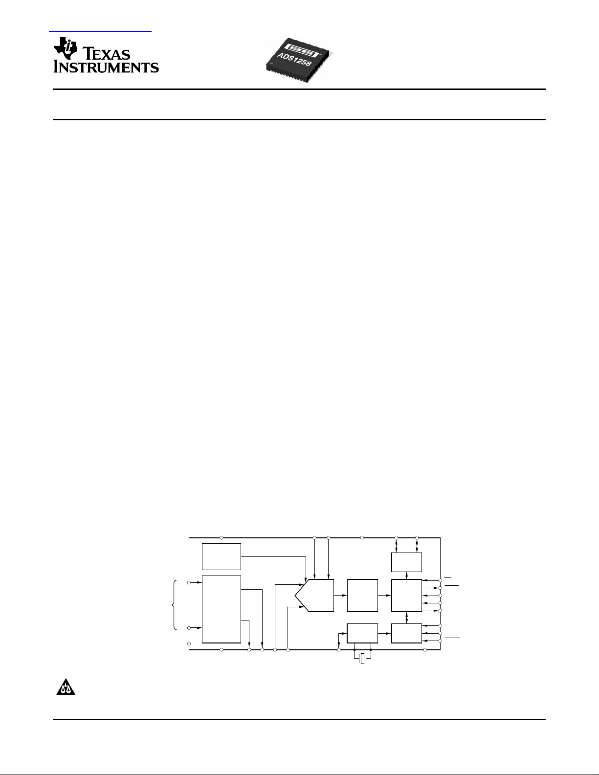
24−Bit
ADC
Digital
Filter
Internal
Monitoring
16:1
Analog
Input
MUX
1
16
AINCOM
…
ADC
In
Extclk
In/Out
AVSS DGND
AVDD DVDD
MUX
Out
SPI
Interface
CS
DRDY
SCLK
DIN
DOU T
ControlOscillator
GPIO
START
RESET
PWDN
GPIO[7:0]V
REF
ADS1258
Analog Inputs
查询ADS1258供应商查询ADS1258供应商
SBAS297A – JUNE 2005 – REVISED SEPTEMBER 2005
16-Channel, 24-Bit Analog-to-Digital Converter
FEATURES DESCRIPTION
• 24 Bits, No Missing Codes
• Fixed-Channel or Automatic Channel Scan
• Fixed-Channel Data Rate: 125kSPS
• Auto-Scan Data Rate: 23.7kSPS
• Single-Conversion Settled Data multiplexer accepts combinations of eight differential
• 16 Single-Ended or 8 Differential Inputs
• Unipolar (+5V) or Bipolar ( ± 2.5V) Operation
• Low Noise: 2.8µV
at 1.8kSPS
RMS
• 0.0003% Integral Nonlinearity
• DC Stability (typical): The differential output of the multiplexer is accessible
0.02µV/ ° C Offset Drift, 0.4ppm/ ° C Gain Drift
• Open-Sensor Detection
• Conversion Control (Pin and Commands)
• Multiplexer Output for External Signal
Conditioning
• On-Chip Temperature, Reference, Offset,
Gain, and Supply Voltage Readback
• 42mW Power Dissipation
• Standby, Sleep, and Power-Down Modes
• 8 General-Purpose Inputs/Outputs (GPIO)
• 32.768kHz Crystal Oscillator or External Clock
The ADS1258 is a 16-channel (multiplexed),
low-noise, 24-bit, delta-sigma ( ∆ Σ ) analog-to-digital
converter (ADC) that provides single-cycle settled
data at channel scan rates from 1.8k to 23.7k
samples per second (SPS). A flexible input
or 16 single-ended inputs with a full-scale differential
range of 5V or true bipolar range of ± 2.5V when
operating with a 5V reference. The fourth-order
delta-sigma modulator is followed by a fifth-order sinc
digital filter optimized for low-noise performance.
to allow signal conditioning prior to the input of the
ADC. Internal system monitor registers provide
supply voltage, temperature, reference voltage, gain,
and offset data.
An onboard PLL generates the system clock from a
32.768kHz crystal, or can be overridden by an
external clock source. A buffered system clock output
(15.7MHz) is provided to drive a microcontroller or
additional converters.
Serial digital communication is handled via an
SPI™-compatible interface. A simple command word
structure controls channel configuration, data rates,
digital I/O, monitor functions, etc.
ADS1258
APPLICATIONS
• Medical, Avionics, and Process Control
• Machine and System Monitoring
• Fast Scan Multi-Channel Instrumentation
• Industrial Process Controls
• Test and Measurement Systems
SPI is a trademark of Motorola, Inc.
All trademarks are the property of their respective owners.
PRODUCTION DATA information is current as of publication date.
Products conform to specifications per the terms of the Texas
Instruments standard warranty. Production processing does not
necessarily include testing of all parameters.
Please be aware that an important notice concerning availability, standard warranty, and use in critical applications of Texas
Instruments semiconductor products and disclaimers thereto appears at the end of this data sheet.
Programmable sensor bias current sources can be
used to bias sensors or verify sensor integrity.
The ADS1258 operates from a unipolar +5V or
bipolar ± 2.5V analog supply and a digital supply
compatible with interfaces ranging from 2.7V to
5.25V. The ADS1258 is available in a QFN-48
package.
Copyright © 2005, Texas Instruments Incorporated
www.ti.com
ADS1258
SBAS297A – JUNE 2005 – REVISED SEPTEMBER 2005
This integrated circuit can be damaged by ESD. Texas Instruments recommends that all integrated
circuits be handled with appropriate precautions. Failure to observe proper handling and installation
procedures can cause damage.
ESD damage can range from subtle performance degradation to complete device failure. Precision
integrated circuits may be more susceptible to damage because very small parametric changes could
cause the device not to meet its published specifications.
ORDERING INFORMATION
For the most current package and ordering information see the Package Option Addendum at the end of this
document, or see the TI web site at www.ti.com .
ABSOLUTE MAXIMUM RATINGS
Over operating free-air temperature range (unless otherwise noted).
AVDD to AVSS –0.3 to +5.5 V
AVSS to DGND –2.8 to +0.3 V
DVDD to DGND –0.3 to +5.5 V
Input Current 100, Momentary mA
Input Current 10, Continuous mA
Analog Input Voltage AVSS – 0.3 to AVDD + 0.3 V
Digital Input Voltage to DGND –0.3 to DVDD + 0.3 V
Maximum Junction Temperature +150 ° C
Operating Temperature Range –40 to +105 ° C
Storage Temperature Range –60 to +150 ° C
Lead Temperature (soldering, 10s) +300 ° C
(1) Stresses above these ratings may cause permanent damage. Exposure to absolute maximum conditions for extended periods may
degrade device reliability. These are stress ratings only, and functional operation of the device at these or any other conditions beyond
those specified is not implied.
(1)
ADS1258 UNIT
2
www.ti.com
SBAS297A – JUNE 2005 – REVISED SEPTEMBER 2005
ELECTRICAL CHARACTERISTICS
All specifications at TA= –40 ° C to +105 ° C, AVDD = +2.5V, AVSS = –2.5V, DVDD = +3.3V, f
OPA227 buffer between MUX outputs and ADC inputs, V
PARAMETER CONDITIONS MIN TYP MAX UNIT
Analog Multiplexer Inputs
Absolute Input Voltage AVSS – 100mV AVDD + 100mV V
AINCOM with respect to DGND
On-Channel Resistance 80 Ω
Crosstalk fIN= 1kHz –110 dB
Sensor Bias (Current Source) µA
1.5 µ A:24 µ A Ratio Error 1 %
ADC Input
Full-Scale Input Voltage (V
IN
Absolute Input Voltage (ADCINP, ADCINN) AVSS – 100mV AVDD + 100mV V
Differential Input Impedance 65 k Ω
System Performance
Resolution No Missing Codes 24 Bits
Data Rate, Fixed-Channel Mode 1.953 125 kSPS
Data Rate, Auto-Scan Mode 1.805 23.739 kSPS
Integral Nonlinearity (INL)
(1)
Offset Error Shorted Inputs µ V
Offset Drift
(3)
Gain Error 0.1 0.5 %
Gain Drift
(3)
Noise (see Table 4 )
Common-Mode Rejection fCM= 60Hz 90 100 dB
Power-Supply Rejection fPS= 60Hz dB
Voltage Reference Input
Reference Input Voltage (V
REF
Negative Reference Input (VREFN) AVSS – 0.1V VREFP – 0.5 V
Positive Reference Input (VREFP) VREFN + 0.5 AVDD + 0.1V V
Reference Input Impedance 40 k Ω
System Parameters
External Reference Reading Error 1 3 %
Analog Supply Reading Error 1 3 %
Temperature Sensor Voltage TA= +25 ° C 168 mV
Reading
Digital Input/Output
Logic Levels: V
Input Leakage VIN= DVDD, GND 10 µA
Master Clock Input (CLKIO)
AIN0–AIN15,
= ADCINP – ADCINN) ± 1.0 6V
Chopping Off 20
Chopping On 1 10
Chopping Off 0.5
Chopping On 0.02 0.1
AVDD, AVSS 70 85
DVDD 80 95
= VREFP – VREFN) 0.5 4.096 AVDD – AVSS V
Coefficient 394 µ V/ ° C
IH
V
IL
V
OH
V
OL
Frequency 0.1 16 MHz
Duty Cycle 40 60 %
= +4.096V, and VREFN = –2.5V, unless otherwise noted.
REF
ADS1258
SBCS[1:0] = 01 1.5
SBCS[1:0] = 11 24
Differential Input 0.0003 0.0010 % of FSR
Shorted Inputs µ V/ ° C
0.7DVDD DVDD V
DGND 0.3DVDD V
IOH= 2mA 0.8DVDD DVDD V
IOL= 2mA DGND 0.2DVDD V
= 16MHz (external clock),
CLK
REF
0.4 2 ppm/ ° C
ADS1258
V
(2)
(1) Best straight line fit method.
(2) FSR = Full-scale range = 2.1 3V
(3) Ensured by characterization.
.
REF
3
www.ti.com
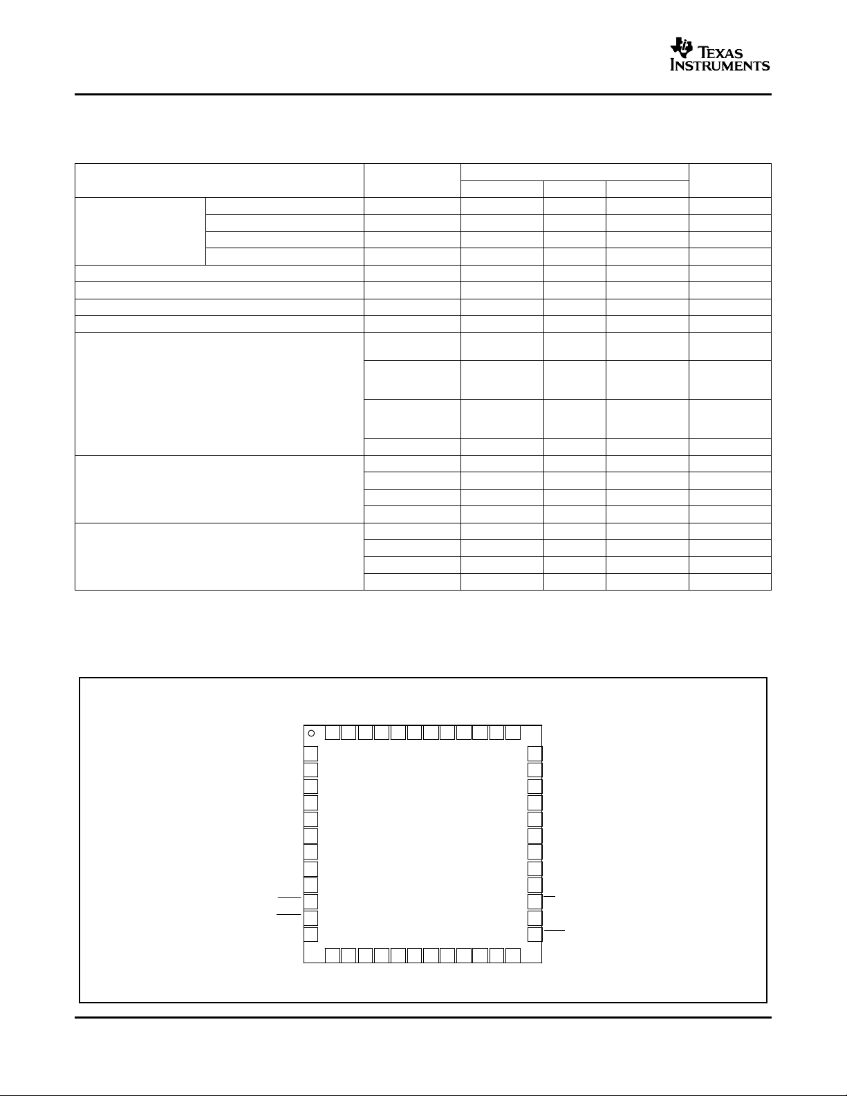
Top View QFN
36
35
34
33
32
31
30
29
28
27
26
25
AIN12
AIN13
AIN14
AIN15
AINCOM
VREFP
VREFN
DGND
DVDD
CS
START
DRDY
AIN4
AIN5
AIN6
AIN7
MUXOUTP
MUXOUTN
ADCINP
ADCINN
AIN8
AIN9
AIN10
AIN11
CLKIO
GPIO0
GPIO1
GPIO2
GPIO3
GPIO4
GPIO5
GPIO6
GPIO7
SCLK
DIN
DOUT
1
2
3
4
5
6
7
8
9
10
11
12
AIN3
AIN2
AIN1
AIN0
AVSS
AVDD
PLLCAP
XTAL1
XTAL2
PWDN
RESET
CLKSEL
48 47 46 45 44 43 42 41 40 39 38
13 14 15 16 17 18 19 20 21 22 233724
ADS1258
ADS1258
SBAS297A – JUNE 2005 – REVISED SEPTEMBER 2005
ELECTRICAL CHARACTERISTICS (continued)
All specifications at TA= –40 ° C to +105 ° C, AVDD = +2.5V, AVSS = –2.5V, DVDD = +3.3V, f
OPA227 buffer between MUX outputs and ADC inputs, V
PARAMETER CONDITIONS MIN TYP MAX UNIT
Crystal Frequency 32.768 kHz
Crystal Oscillator
(see Crystal Oscillator
section)
Start-Up Time (Clock Output Valid) 150 mS
Power Supply
DVDD 2.7 5.25 V
AVSS –2.6 0 V
AVDD AVSS + 4.75 AVSS + 5.25 V
DVDD Supply Current
AVDD, AVSS Supply Current
Power Dissipation
Clock Output Frequency 15.729 MHz
Clock Output Duty Cycle 40 60 %
= +4.096V, and VREFN = –2.5V, unless otherwise noted.
REF
ADS1258
External Clock
Operation
Internal Oscillator
Operation, Clock 0.04 mA
Output Disabled
Internal Oscillator
Operation, Clock 1.4 mA
Output Enabled
Power-Down
(4)
(5)
Converting 8.2 12 mA
Standby 5.6 mA
Sleep 2.1 mA
Power-Down 2 85 µA
Converting 42 62 mW
Standby 29 mW
Sleep 11 mW
Power-Down 14 µ W
= 16MHz (external clock),
CLK
0.25 0.6 mA
1 25 µA
(4) CLKIO load = 20pF.
(5) No clock applied to CLKIO.
PIN CONFIGURATION
4
www.ti.com
SBAS297A – JUNE 2005 – REVISED SEPTEMBER 2005
PIN ASSIGNMENTS
PIN # NAME INPUT/OUTPUT DESCRIPTION
1 AIN3 Analog Input Analog Input 3: Single-Ended Channel 3, Differential Channel 1 (–)
2 AIN2 Analog Input Analog Input 2: Single-Ended Channel 2, Differential Channel 1 (+)
3 AIN1 Analog Input Analog Input 1: Single-Ended Channel 1, Differential Channel 0 (–)
4 AIN0 Analog Input Analog Input 0: Single-Ended Channel 0, Differential Channel 0 (+)
5 AVSS Analog
6 AVDD Analog Positive Analog Power Supply: +5V for unipolar operation, +2.5V for bipolar operation.
7 PLLCAP Analog PLL Bypass Capacitor: Connect 22nF capacitor to AVSS when using crystal oscillator.
8 XTAL1 Analog 32.768kHz Crystal Oscillator Input 1; see Crystal Oscillator section.
9 XTAL2 Analog 32.768kHz Crystal Oscillator Input 2; see Crystal Oscillator section.
10 PWDN Digital Input Power-Down Input: Hold low for minimum of two f
11 RESET Digital Input Reset Input: Hold low for minimum of two f
12 CLKSEL Digital Input
13 CLKIO Digital I/O System Clock Input/Output (See CLKSEL pin.)
14 GPIO0 Digital I/O General-Purpose Digital Input/Output 0
15 GPIO1 Digital I/O General-Purpose Digital Input/Output 1
16 GPIO2 Digital I/O General-Purpose Digital Input/Output 2
17 GPIO3 Digital I/O General-Purpose Digital Input/Output 3
18 GPIO4 Digital I/O General-Purpose Digital Input/Output 4
19 GPIO5 Digital I/O General-Purpose Digital Input/Output 5
20 GPIO6 Digital I/O General-Purpose Digital Input/Output 6
21 GPIO7 Digital I/O General-Purpose Digital Input/Output 7
22 SCLK Digital Input SPI Interface Clock Input: Data clocked in on rising edge, clocked out on falling edge.
23 DIN Digital Input SPI Interface Data Input: Data is input to the device.
24 DOUT Digital Output SPI Interface Data Output: Data is output from the device.
25 DRDY Digital Output Data Ready Output: Active low.
26 START Digital Input Start Conversion Input: Active high.
27 CS Digital Input SPI Interface Chip Select Input: Active low.
28 DVDD Digital Digital Power Supply: 2.7V to 5.25V
29 DGND Digital Digital Ground
30 VREFN Analog Input Reference Input Negative
31 VREFP Analog Input Reference Input Positive
32 AINCOM Analog Input Analog Input Common: Common input pin to all single-ended inputs.
33 AIN15 Analog Input Analog Input 15: Single-Ended Channel 15, Differential Channel 7 (–)
34 AIN14 Analog Input Analog Input 14: Single-Ended Channel 14, Differential Channel 7 (+)
35 AIN13 Analog Input Analog Input 13: Single-Ended Channel 13, Differential Channel 6 (–)
36 AIN12 Analog Input Analog Input 12: Single-Ended Channel 12, Differential Channel 6 (+)
37 AIN11 Analog Input Analog Input 11: Single-Ended Channel 11, Differential Channel 5 (–)
38 AIN10 Analog Input Analog Input 10: Single-Ended Channel 10, Differential Channel 5 (+)
39 AIN9 Analog Input Analog Input 9: Single-Ended Channel 9, Differential Channel 4 (–)
40 AIN8 Analog Input Analog Input 8: Single-Ended Channel 8, Differential Channel 4 (+)
41 ADCINN Analog Input ADC Differential Input (–)
42 ADCINP Analog Input ADC Differential Input (+)
43 MUXOUTN Analog Output Multiplexer Differential Output (–)
44 MUXOUTP Analog Output Multiplexer Differential Output (+)
45 AIN7 Analog Input Analog Input 7: Single-Ended Channel 7, Differential Channel 3 (–)
46 AIN6 Analog Input Analog Input 6 : Single-Ended Channel 6, Differential Channel 3 (+)
47 AIN5 Analog Input Analog Input 5: Single-Ended Channel 5, Differential Channel 2 (–)
48 AIN4 Analog Input Analog Input 4: Single-Ended Channel 4, Differential Channel 2 (+)
ANALOG/DIGITAL
Negative Analog Power Supply: 0V for unipolar operation, –2.5V for bipolar operation.
(Internally connected to exposed thermal pad of QFN package.)
cycles to engage low-power mode.
CLK
cycles to reset the device.
CLK
Clock Select Input: Low = Activates Crystal Oscillator, f
High = Disables Crystal Oscillator, apply f
to CLKIO.
CLK
output on CLKIO.
CLK
ADS1258
5
www.ti.com
SCLK
CS
(1)
DIN
DOUT
t
SCLK
t
CSSC
t
SPW
t
DIST
t
DIHD
t
SPW
t
CSDO
t
DOPD
t
DOHD
NOTE: (1) CS can be tied low.
DRDY
DOUT
t
DRDY
t
DDO
ADS1258
SBAS297A – JUNE 2005 – REVISED SEPTEMBER 2005
PARAMETER MEASUREMENT INFORMATION
Figure 1. Serial Interface Timing
SERIAL INTERFACE TIMING CHARACTERISTICS
SYMBOL DESCRIPTION MIN MAX UNITS
t
SCLK
t
SPW
t
CSSC
t
DIST
t
DIHD
t
DOPD
t
DOHD
t
CSDO
(1) τ
CLK
(2) Programmable to 256 τ
(3) CS can be tied low.
(4) DOUT load = 20 pF || 100k Ω to DGND.
SCLK Period 2 τ
SCLK High or Low Pulse Width (exceeding max resets SPI interface) 0.8 4096
CS Low to First SCLK: Setup Time
(3)
0.5 τ
Valid DIN to SCLK Rising Edge: Setup Time 10 ns
Valid DIN to SCLK Rising Edge: Hold Time 5 ns
SCLK Falling Edge to Valid New DOUT: Propagation Delay
(4)
SCLK Falling Edge to Old DOUT Invalid: Hold Time 0 ns
CS High to DOUT Invalid (tri-state) 5 τ
= master clock period = 1/f
CLK
.
CLK
.
(2)
5 ns
(1)
CLK
τ
CLK
CLK
CLK
Figure 2. DRDY Update Timing
DRDY UPDATE TIMING CHARACTERISTICS
SYMBOL DESCRIPTION TYP UNITS
t
DRDY
t
DDO
6
DRDY High Pulse Width Without Data Read 1 τ
Valid DOUT to DRDY Falling Edge ( CS = 0) 0.5 τ
CLK
CLK
www.ti.com
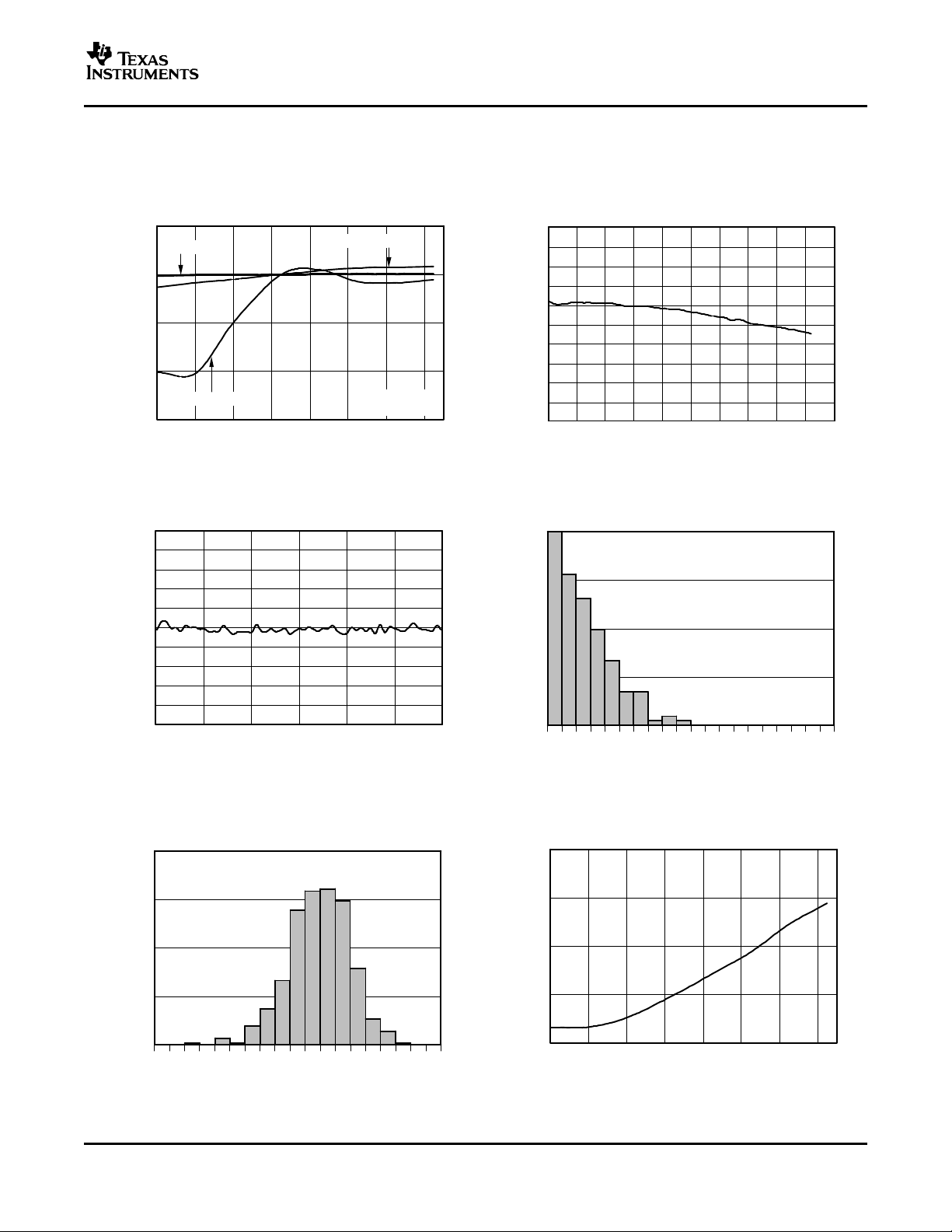
TYPICAL CHARACTERISTICS
Number of Occurences
Offset (µV)
3000
2500
2000
1500
1000
500
0
−
50
−
45
−
40
−
35
−
30
−
25
−
20
−
15
−
10
505
10
15
20
25
30
35
40
45
50
DRATE[1:0] = 11
16384 Points
Number of Occurences
Offset (µV)
4500
4000
3500
3000
2500
2000
1500
1000
500
0
−
35
−
30
−
25
−
20
−
15
−
10
−
5
0
5
10
15
20
25
30
35
DRATE[1:0] = 10
16384 Points
Number of Occurences
Offset (µV)
3500
3000
2500
2000
1500
1000
500
0
−
20
−
16
−
12
−
8
−
4
0
4
8
12
16
20
DRATE[1:0] = 01
16384 Points
Number of Occurences
Offset (µV)
2500
2000
1500
1000
500
0
−
12
−
10
−
8
−
6
−
4
−
2
0
2
4
6
8
10
12
DRATE[1:0] = 00
16384 Points
RMS Noise (
µ
V)
Input Voltage (%FS)
20
15
10
5
0
−
100−75 10075
−50−
25 50250
DRATE[1:0] = 11
DRATE[1:0] = 10
DRATE[1:0] = 01
DRATE[1:0] = 00
Number of Occurences
RMS Noise (µV)
20
15
10
5
0
10.0
10.5
11.0
11.5
12.0
12.5
13.0
13.5
14.0
14.5
15.0
50 units from twoproduction lots.
DRATE[1:0] = 11
At TA= +25 ° C, AVDD = +2.5V, AVSS = –2.5V, DVDD = +3.3V, f
outputs and ADC inputs, VREFP = +2.048V, and VREFN = –2.048V, unless otherwise noted.
READING HISTOGRAM READING HISTOGRAM
Figure 3. Figure 4.
SBAS297A – JUNE 2005 – REVISED SEPTEMBER 2005
= 16MHz (external), OPA227 buffer between MUX
CLK
ADS1258
READING HISTOGRAM READING HISTOGRAM
Figure 5. Figure 6.
NOISE HISTOGRAM NOISE vs INPUT VOLTAGE
Figure 7. Figure 8.
7
www.ti.com
RMS Noise (
µ
V)
V
REF
(V)
16
14
12
10
8
6
4
2
0
0.5 1.5 5.52.5 3.5 4.5
DRATE[1:0] = 11
DRATE[1:0] = 10
DRATE[1:0] = 01
DRATE[1:0] = 00
RMS Noise (
µ
V)
DVDD, AVDD−AVSS (V)
20
18
16
14
12
10
8
6
4
2.5 3.0 5.53.5 4.0 4.5 5.0
DRATE[1:0] = 11
from DVDD
from AVDD−AVSS
RMS Noise (
µ
V)
Temperature (C)
20
18
16
14
12
10
8
6
4
−40−
20 0
20 40 60 80 100
DRATE[1:0] = 11
RMS Noise (
µ
V)
Common−Mode Input Voltage(V)
20
15
10
5
0
Offset (
µ
V)
5
0
−
5
−
10
−
15
−
3
−
2 3
−
1 0 1 2
OFFSET
CHOP = 1
OFFSET
CHOP = 0
NOISE
Number of Occurences
Offset (µV)
200
180
160
140
120
100
80
60
40
20
0
−
10
−
8
−
6
−
4
−
2
0
2
4
6
8
10
311 units fromone production lot.
CHOP = 1
Number of Occurences
Offset Drift (µV/C)
80
60
40
20
0
−
0.10
−
0.09
−
0.08
−
0.07
−
0.06
−
0.05
−
0.04
−
0.03
−
0.02
−
0.01
0
0.01
0.02
0.03
0.04
0.05
0.06
0.07
0.08
0.09
0.10
50 units from two
production lots.
Based on 20C intervals
over the range of
−
40C to +105C.
CHOP = 1
ADS1258
SBAS297A – JUNE 2005 – REVISED SEPTEMBER 2005
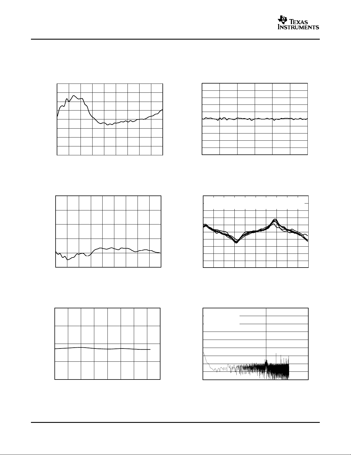
TYPICAL CHARACTERISTICS (continued)
At TA= +25 ° C, AVDD = +2.5V, AVSS = –2.5V, DVDD = +3.3V, f
outputs and ADC inputs, VREFP = +2.048V, and VREFN = –2.048V, unless otherwise noted.
= 16MHz (external), OPA227 buffer between MUX
CLK
NOISE vs V
REF
NOISE vs SUPPLY VOLTAGE
Figure 9. Figure 10.
NOISE AND OFFSET vs
NOISE vs TEMPERATURE COMMON-MODE INPUT VOLTAGE
8
Figure 11. Figure 12.
OFFSET HISTOGRAM OFFSET DRIFT HISTOGRAM
Figure 13. Figure 14.
www.ti.com
Normalized Offset (
µ
V)
Temperature (C)
20
0
−
20
−
40
−
60
−
40−20 100
0 20 806040
CHOP = 1
CHOP = 1, NoBuffer
CHOP = 0, No Buffer
50 Units from
2 Production Lots
Normalized Offset (
µ
V)
V
REF
(V)
0.5 1.0
10
8
6
4
2
0
−
2
−
4
−
6
−
8
−
10
5.51.5 2.0 2.5 3.0 3.5 4.0 4.5 5.0
Normalized Offset (
µ
V)
Time After Power−On (s)
10
8
6
4
2
0
−
2
−
4
−
6
−
8
−
10
0 10 6020 30 40 50
Free−Air
Number of Occurences
Absolute Gain Error (ppm)
80
60
40
20
0
100
300
500
700
900
1100
1300
1500
1700
1900
320 units from one production lot.
Normalized Gain Error (ppm)
Temperature (C)
30
20
10
0
−
10
−
40−20 100
0 20 806040
Number of Occurences
Gain Drift (ppm/C)
80
60
40
20
0
−
1.8
−
1.6
−
1.4
−
1.2
−
1.0
−
0.8
−
0.6
−
0.4
−
0.2
0
0.2
0.4
0.6
0.8
1.0
1.2
1.4
1.6
1.8
50 units from two production lots.
Based on 20C intervals over the
range of−40C to +105C.
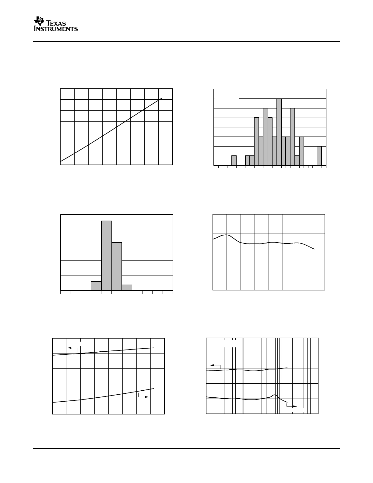
TYPICAL CHARACTERISTICS (continued)
At TA= +25 ° C, AVDD = +2.5V, AVSS = –2.5V, DVDD = +3.3V, f
outputs and ADC inputs, VREFP = +2.048V, and VREFN = –2.048V, unless otherwise noted.
= 16MHz (external), OPA227 buffer between MUX
CLK
ADS1258
SBAS297A – JUNE 2005 – REVISED SEPTEMBER 2005
OFFSET vs TEMPERATURE OFFSET vs V
Figure 15. Figure 16.
OFFSET POWER-ON WARMUP GAIN ERROR HISTOGRAM
REF
GAIN DRIFT HISTOGRAM GAIN ERROR vs TEMPERATURE
Figure 17. Figure 18.
Figure 19. Figure 20.
9
www.ti.com
Normalized Gain Error (ppm)
V
REF
(V)
20
15
10
5
0
−
5
−
10
−
15
−
20
0.5 1.0 5.01.5 2.0 2.5 3.0 3.5 4.0 4.5
Normalized Gain Error (ppm)
Time After Power−On (s)
10
8
6
4
2
0
−
2
−
4
−
6
−
8
−
10
0 10 6020 30 40 50
Free−Air
Linearity Error (ppm)
V
REF
(V)
10
8
6
4
2
0
0.5 1.0 5.01.5 2.0 2.5 3.0 3.5 4.0 4.5
Linearity Error (ppm)
VIN(V)
−5−
4
10
8
6
4
2
0
−
2
−
4
−
6
−
8
−
10
5
−3−2−
1 0 1 2 3 4
V
REF
= 5V
TA=−40C,−10C, +25C, +55C, +85C, +105C
INL (ppm)
Temperature (C)
8
6
4
2
0
−40−
20 120100
0 20 806040
Level (dBFS)
Frequency (Hz)
0
−
20
−
40
−
60
−
80
−
100
−
120
−
140
−
160
−
180
1 10 100k100 1k 10k
f = 1kHz,−0.5dBFs
DRATE[1:0] = 11
65536 Points
ADS1258
SBAS297A – JUNE 2005 – REVISED SEPTEMBER 2005
TYPICAL CHARACTERISTICS (continued)
At TA= +25 ° C, AVDD = +2.5V, AVSS = –2.5V, DVDD = +3.3V, f
outputs and ADC inputs, VREFP = +2.048V, and VREFN = –2.048V, unless otherwise noted.
= 16MHz (external), OPA227 buffer between MUX
CLK
GAIN ERROR vs V
REF
Figure 21. Figure 22.
INTEGRAL NONLINEARITY vs V
GAIN ERROR POWER-ON WARMUP
REF
INTEGRAL NONLINEARITY vs INPUT LEVEL
INTEGRAL NONLINEARITY vs TEMPERATURE OUTPUT SPECTRUM
10
Figure 23. Figure 24.
Figure 25. Figure 26.
www.ti.com
Temperature Sensor Voltage (mV)
Temperature (C)
210
200
190
180
170
160
150
140
−40−
20 12040
0 20 60 80 100
Number of Occurences
Temperature Reading (C)
8
7
6
5
4
3
2
1
0
12
13
14
15
16
17
18
19
20
21
22
23
24
25
26
27
28
29
30
31
32
33
34
35
36
50 units from two production lots.
TA= +25C
Ratio (
µ
A/
µ
A)
Temperature (C)
18
17
16
15
14
−40−
20 120100
0 20 806040
Number of Occurences
Ratio (µA/µA)
25
20
15
10
5
0
14.0
14.5
15.0
15.5
16.0
16.5
17.0
17.5
18.0
18.5
19.0
50 units from two production lots.
AVDD, AVSS Current (mA)
Temperature (C)
10
8
6
4
2
0
DVDD Current (mA)
1.0
0.8
0.6
0.4
0.2
0
−40−
20 1200 20 40 60 80 100
AVDD, AVSS
DVDD
RMS Noise (
µ
V)
Master Clock (MHz)
20
16
12
8
4
0
Linearity Error (ppm)
20
16
12
8
4
0
0.1 1 10010
DRATE[1:0] = 11
Noise
Linearity
TYPICAL CHARACTERISTICS (continued)
At TA= +25 ° C, AVDD = +2.5V, AVSS = –2.5V, DVDD = +3.3V, f
outputs and ADC inputs, VREFP = +2.048V, and VREFN = –2.048V, unless otherwise noted.
TEMPERATURE SENSOR VOLTAGE vs TEMPERATURE TEMPERATURE SENSOR READING HISTOGRAM
Figure 27. Figure 28.
= 16MHz (external), OPA227 buffer between MUX
CLK
ADS1258
SBAS297A – JUNE 2005 – REVISED SEPTEMBER 2005
SENSOR BIAS CURRENT SOURCE RATIO SENSOR BIAS CURRENT SOURCE RATIO
HISTOGRAM vs TEMPERATURE
Figure 29. Figure 30.
SUPPLY CURRENT vs TEMPERATURE NOISE AND INL vs MASTER CLOCK
Figure 31. Figure 32.
11
www.ti.com
AIN0
AIN1
AIN2
AIN3
AIN4
AIN5
AIN6
AIN7
AIN8
AIN9
AIN10
AIN11
AIN12
AIN13
AIN14
AIN15
AINCOM
Control
Logic
VREFPVREFN
AVSS
PLLCAP XTAL1XTAL2
DRDY
PWDN
RESET
START
SPI
Interface
CS
SCLK
DIN
DOUT
Digital Filter
Clock Control
16−Channel
MUX
AVDD
Sensor
Bias
M
UXOUTP
MUX
OUTN
ADCINP GND
AD
CINN
ADC Channel Control
Supply Monitor
GPIO
G
PIO[7:0]
DVDD
Temperature
Ext Ref Monitor
Internal Ref
ADC
CLKSELCLKIO
ADS1258
SBAS297A – JUNE 2005 – REVISED SEPTEMBER 2005
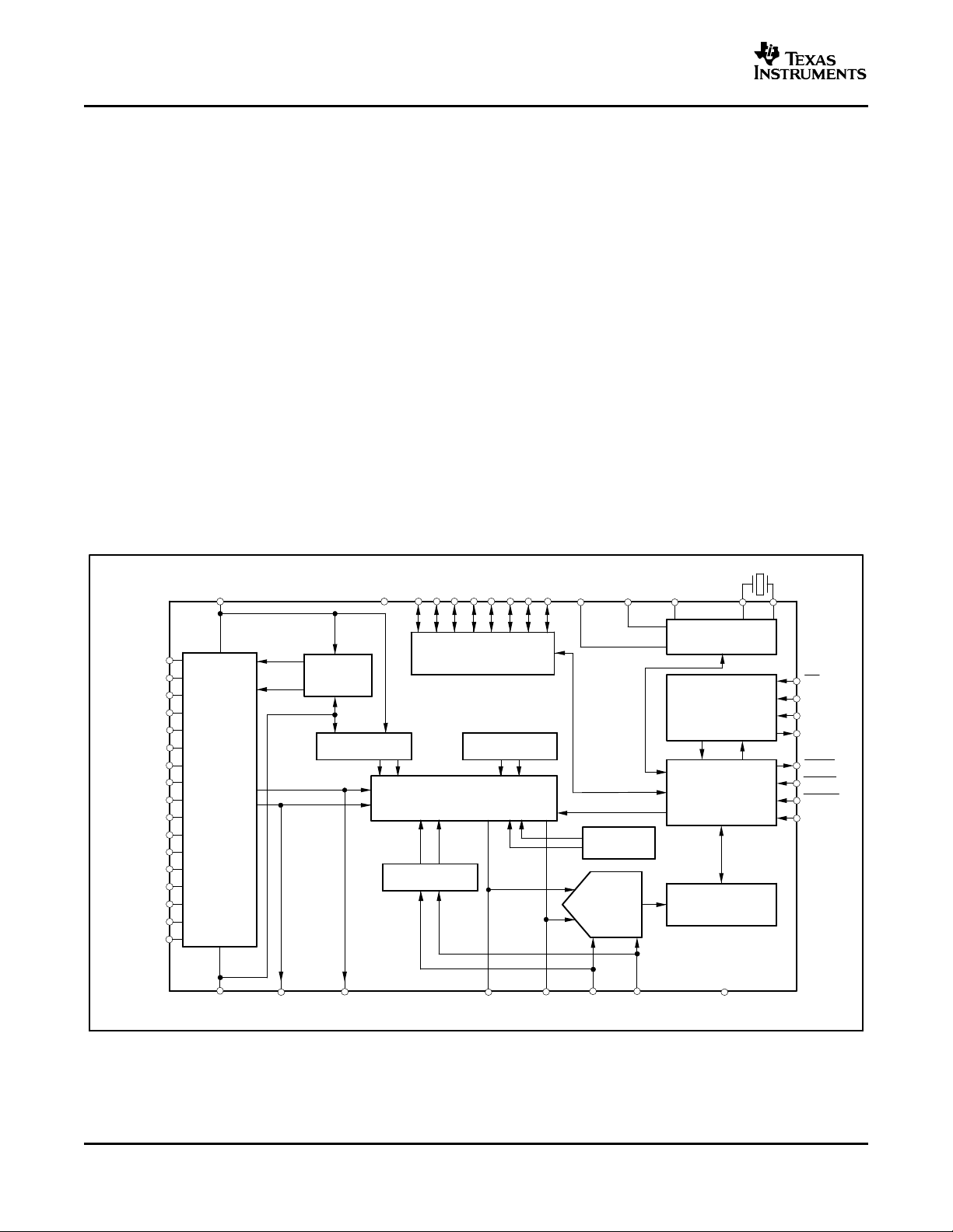
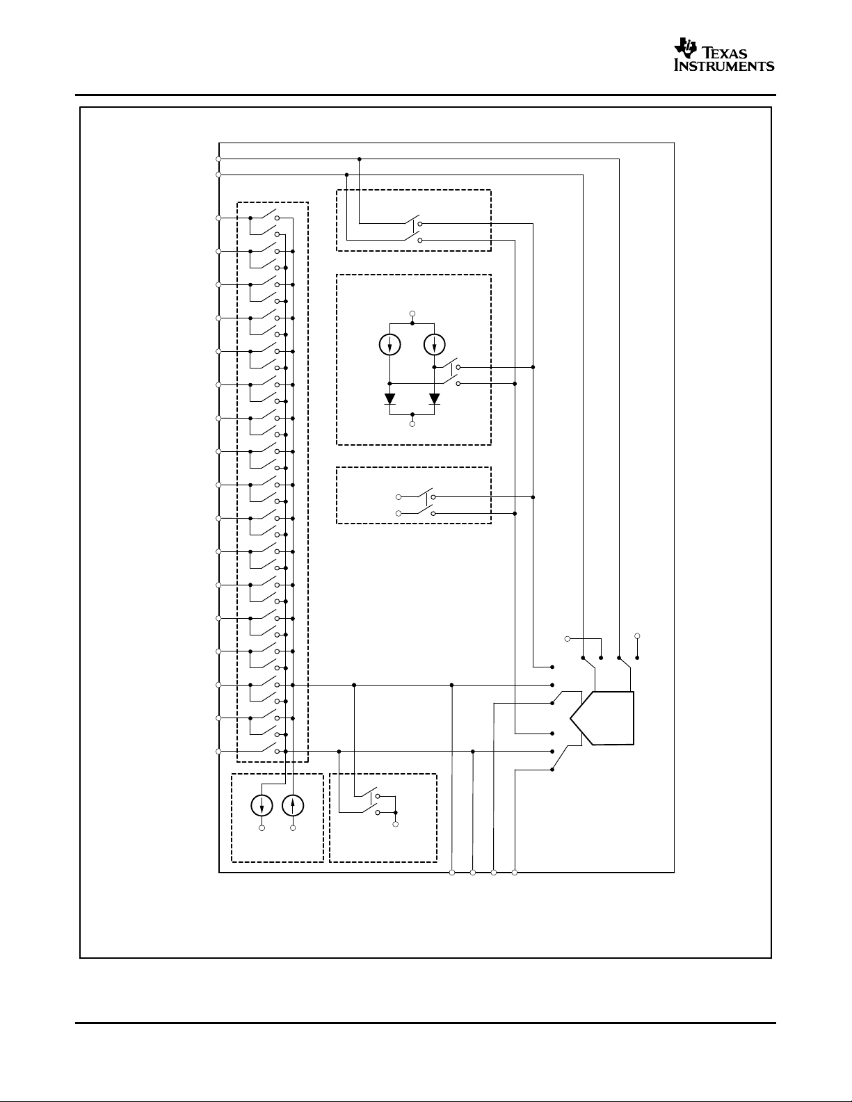
The ADS1258 is a flexible, 24-bit, low-noise ADC
optimized for fast multi-channel, high-resolution
measurement systems. The converter provides a
maximum channel scan rate of 23.7kSPS, providing a
complete 16-channel scan in less than 700µs.
Figure 33 shows the block diagram of the ADS1258.
The input multiplexer selects the analog input pins
connected to the multiplexer output pins
(MUXOUTP/MUXOUTN). External signal conditioning
can be used between the multiplexer output pins and
the ADC input pins (ADCINP/ADCINN) or the
multiplexer output can be routed internally to the ADC
inputs without external circuitry. Selectable current
sources within the input multiplexer can be used to
bias sensors or detect for a failed sensor. On-chip
system function readings provide readback of
temperature, supply voltage, gain, offset, and external
reference. The ADS1258 converter is comprised of a
fourth-order, delta-sigma modulator followed by a
programmable digital filter. The modulator measures
the differential input signal V
against the differential reference input V
IN
= (ADCINP – ADCINN)
REF
OVERVIEW
(VREFP – VREFN). The digital filter receives the
modulator signal and provides a low-noise digital
output. The ADC channel block controls the
multiplexer Auto-Scan feature. Channel Auto-Scan
occurs at a maximum rate of 23.7kSPS. Slower scan
rates can be used with corresponding increases in
resolution.
Communication is handled over an SPI-compatible
serial interface with a set of simple commands
providing control of the ADS1258. Onboard registers
store the various settings for the input multiplexer,
sensor detect bias, data rate selection, etc. Either an
external 32.768kHz crystal, connected to pins XTAL1
and XTAL2, or an external clock applied to pin CLKIO
can be used as the clock source. When using the
external crystal oscillator, the system clock is
available as an output for driving other devices or
controllers. General-purpose digital I/Os (GPIO)
provide input and output control of eight pins.
=
12
Figure 33. ADS1258 Block Diagram
www.ti.com
AVSS 100mV VREFP or VREFN AVDD 100mV
ESD
Diodes
ESD
Diodes
3pF
R
eff
= 40k
Ω
(f
CLK
= 16MHz)
AVDD
AVSS
VREFP
VREFN
ADS1258
SBAS297A – JUNE 2005 – REVISED SEPTEMBER 2005
MULTIPLEXER INPUTS
A simplified diagram of the input multiplexer is
illustrated in Figure 35 . The multiplexer connects one
of 16 single-ended external inputs, one of eight
differential external inputs, or one of the on-chip
internal variables to the ADC inputs. The output of the
channel multiplexer can be routed to external pins
and then to the input of the ADC. This flexibility
allows for use of external signal conditioning. See the
External Multiplexer Loop section.
ESD diodes protect the analog inputs. To keep these
diodes from turning on, make sure the voltages on
the input pins do not go below AVSS by more than
100mV, and likewise do not exceed AVDD by more
than 100mV:
AVSS – 100mV < (Analog Inputs) < AVDD + 100mV.
The converter supports two modes of channel access
through the multiplexer: the Auto-Scan mode and the
Fixed-Channel mode. These modes are selected by
the MUXMOD bit of register CONFIG0. The
Auto-Scan mode scans through the selected
channels automatically, with break-before-make
switching. The Fixed-Channel mode requires the user
to set the channel address for each channel
measured.
ESD diodes protect the reference inputs. To keep
these diodes from turning on, make sure the voltages
on the reference pins do not go below AVSS by more
than 100mV, and likewise do not exceed AVDD by
100mV, as described in Equation 1 :
(1)
A high-quality reference voltage is essential for
achieving the best performance from the ADS1258.
Noise and drift on the reference degrade overall
system performance. It is especially critical that
special care be given to the circuitry that generates
the reference voltages and the layout when operating
in the low-noise settings (that is, with low data rates)
to prevent the voltage reference from limiting
performance. See the Reference Inputs description in
the Hardware Considerations segment of the
Applications section.
VOLTAGE REFERENCE INPUTS
(VREFP, VREFN)
The voltage reference for the ADS1258 ADC is the
differential voltage between VREFP and VREFN:
V
= VREFP – VREFN. The reference inputs use a
REF
structure similar to that of the analog inputs with the
circuitry on the reference inputs shown in Figure 34 .
The load presented by the switched capacitor can be
modeled with an effective resistance (R
f
= 16MHz. Note that the effective impedance of
CLK
the reference inputs will load an external reference
with a non-zero source impedance.
) of 40k Ω for
eff
Figure 34. Simplified Reference Input Circuit
13
www.ti.com
ADC
AIN0
VREFN
VREFP
AIN1
AIN2
AIN3
AIN4
AIN5
AIN6
AIN7
AIN8
AIN9
AIN10
AIN11
AIN12
AIN13
AIN14
AIN15
AINCOM
Multiplexer
Reference/Gain Monitor
NOTE: ESD diodes not shown.
Supply Monitor
AVDD
AVSS
AVDD
AVSS
Temperature Sensor Monitor
1x 2x
8x 1x
AVDD
(AVDD−AVSS)/2
AVSS
Sensor Bias Offset Monitor
MUXOUTP
MUXOUTN
ADCINP
ADCINN
Internal
Reference
AVSS
ADS1258
SBAS297A – JUNE 2005 – REVISED SEPTEMBER 2005
Figure 35. Input Multiplexer
14
www.ti.com
t
SAMPLE
ON
OFF
S
1
S
2
OFF
ON
S
1
S
1
AVSS + 1.3V
R
AIN
= R
effB
|| 2R
effA
AVSS + 1.3V
R
effA
= 190k
Ω
R
effB
= 78kΩ(f
CLK
= 16MHz)
R
effA
= 190k
Ω
ADCINN
ADCINP
CA1= 0.65pF
CB= 1.6pF
C
A2
= 0.65pF
ADCINN
S
2
AVSS + 1.3V
S
2
AVSS + 1.3V
ADCINP
Equivalent
Circuit
R
eff
= t
SAMPLE/CX
NOTE: ESD input diodes not shown.
ADS1258
SBAS297A – JUNE 2005 – REVISED SEPTEMBER 2005
ADC INPUTS
The ADS1258 ADC inputs (ADCINP, ADCINN)
measure the input signal using internal capacitors
R
= V
eff
with f
IN/IAVERAGE
. For example, if f
CLK
two, the impedances will double.
. These impedances scale inversely
is reduced by a factor of
CLK
that are continuously charged and discharged. The As with the multiplexer and reference inputs, ESD
left side of Figure 37 shows a simplified schematic of diodes protect the ADC inputs. To keep these diodes
the ADC input circuitry; the right side of Figure 37 from turning on, make sure the voltages on the input
shows the input circuitry with the capacitors and pins do not go below AVSS by more than 100mV,
switches replaced by an equivalent circuit. Figure 36 and likewise do not exceed AVDD by more than
shows the ON/OFF timings of the switches shown in 100mV.
Figure 37 . S
sampling phase. With S
ADCINP, C
(ADCINP – ADCINN). For the discharge phase, S
opens first and then S
to approximately AVSS + 1.3V and C
switches close during the input
1
charges to ADCINN, and C
A2
2
1
closes. C
closed, C
charges to
A1
charges to
B
and C
A1
discharge
A2
discharges to
B
1
0V. This two-phase sample/discharge cycle repeats
with a period of t
SAMPLE
= 2/f
.
CLK
The charging of the input capacitors draws a transient
current from the source driving the ADS1258 ADC
inputs. The average value of this current can be used
to calculate an effective impedance (R
) where
eff
Figure 36. S1and S
Switch Timing for Figure 37
2
Figure 37. Simplified ADC Input Structure
15

www.ti.com
50
Ω
32.768kHz
(1)
4.7pF 4.7pF
22nF
CLKSEL XTAL1 XTAL2 PLLCAP
AVSS
CLKIO
ClockOutput
(15.729MHz)
0Vto−2.5V
NOTE:(1)Parallelresonant type, C
L
=12.5pF, ESR = 35kΩ(max).
Placethe crystalandloadcapacitorsas closeas possibleto thedevicepins.
32.768kHz
Crystal Oscillator
and PLL
MUX
CLKENB Bit
Internal Master Clock (f
CLK
)
CLKSEL
CLKIO
XTAL1 XTAL2 PLL
50
Ω
CLKSEL XTAL1 XTAL2 PLLCAP
DVDD
CLKIO
Clock Input
(16MHz)
2.7V
to 5V
No Connection
ADS1258
SBAS297A – JUNE 2005 – REVISED SEPTEMBER 2005
MASTER CLOCK (f
)
CLK
The ADS1258 oversamples the analog input at a high
rate. This requires a high-frequency master clock to
be supplied to the converter. As shown in Figure 38 ,
the clock comes from either a crystal oscillator or an
external clock source.
Figure 38. Clock Generation Block Diagram
Figure 39. Crystal Oscillator Connection
Table 1. System Clock Source
CLKSEL CLKENB
PIN CLOCK SOURCE BIT CLKIO FUNCTION
0 0
0 1 Output (15.729MHz)
1 External Clock Input X Input (16MHz)
32.768kHz Disabled
Crystal Oscillator (internally grounded)
32.768kHz
Crystal Oscillator
The CLKSEL pin determines the source of the
system clock, as shown in Table 1 . The CLKIO pin
functions as an input or as an output. When the
CLKSEL pin is set to '1', CLKIO is configured as an
input to receive the master clock. When the CLKSEL
pin is set to '0', the crystal oscillator generates the
clock. The CLKIO pin can then be configured to
output the master clock. When the clock output is not
needed, it can be disabled to reduce device power
consumption.
Crystal Oscillator
An on-chip oscillator and Phase-Locked Loop (PLL)
can be used to generate the system clock. For this
mode, tie the CLKSEL pin low. A 22nF PLL filter
capacitor, connected from the PLLCAP pin to the
AVSS pin, is required. The internal clock of the PLL
can be output to the CLKIO to drive other converters
or controllers. If not used, disable the clock output to
reduce device power consumption; see Table 1 for
settings. The clock output is enabled by a register bit
setting (default is ON). Figure 39 shows the oscillator
connections. Place these components as close to the
pins as possible to avoid interference and coupling.
Do not connect XTAL1 or XTAL2 to any other logic.
The oscillator start-up time may vary depending on
the crystal and ambient temperature. The user should
verify the oscillator start-up time.
16
Table 2. Approved Crystal Vendors
VENDOR CRYSTAL PRODUCT
Epson C-001R
External Clock Input
When using an external clock to operate the device,
apply the master clock to the CLKIO pin. For this
mode, the CLKSEL pin is tied high. CLKIO then
becomes an input, as shown in Figure 40 .
Make sure to use a clock source clean from jitter or
interference. Ringing or under/overshoot should be
avoided. A 50 Ω resistor in series with the CLKIO pin
(placed close to the source) can often help.
Figure 40. External Clock Connection

www.ti.com
f
CLK
128(4
11bDR
4.265625 TD) 2
CHOP
f
CLK
128(4
11bDR
CHOP(4.265625 TD)) 2
CHOP
Analog
Modulator
sinc
5
Filter
Programmable
Averager
Data Rate = f
CLK
/128Modulator Rate = f
CLK
/2
Num_Ave
Data Rate
(1)
= f
CLK
/(128×Num_Ave)
NOTE: (1) Data rate for Fixed−Channel Mode, Chop = 0, Delay = 0.
ADS1258
SBAS297A – JUNE 2005 – REVISED SEPTEMBER 2005
ADC
The ADC block of the ADS1258 is composed of two
blocks: a modulator and a digital filter.
Modulator
The modulator converts the analog input voltage into
a Pulse Code Modulated (PCM) data stream. When
the level of differential analog input (ADCINP –
ADCINN) is near the level of the reference voltage,
the '1' density of the PCM data stream is at its
highest. When the level of the differential analog input
is near zero, the PCM '0' and '1' densities are nearly Data Rate (Auto-Scan):
equal. The fourth-order modulator shifts the
quantization noise to a high frequency (out of the
passband) where the digital filter can easily remove it.
The modulator continuously chops the input, resulting
in excellent offset and offset drift performance. It is
important to note that offset or offset drift originating
from the external circuitry is not removed by the
modulator chopping. These errors can be effectively
removed by using the external chopping feature of
the ADS1258 (see the External Chopping section).
Digital Filter
The programmable low-pass digital filter receives the
modulator output and produces a high-resolution
digital output. By adjusting the amount of filtering,
tradeoffs can be made between resolution and data
rate: filter more for higher resolution, filter less for
higher data rate. The filter is comprised of two
sections, a fixed filter followed by a programmable
filter. Figure 41 shows the block diagram of the filter.
Data is supplied to the filter from the analog
modulator at a rate of f
/2. The fixed filter is a
CLK
fifth-order sinc filter with a decimation value of 64 that
outputs data at a rate of f
/128. The second stage
CLK
of the filter is a programmable averager (first-order
sinc filter) with the number of averages set by the
DRATE[1:0] bits.
The data rate depends upon the system clock
frequency (f
) and the converter configuration. The
CLK
data rate can be computed by Equation 2 or
Equation 3 :
Data Rate (Fixed-Channel Mode):
where:
• DR = DRATE[1:0] register bits (binary);
• CHOP = Chop register bit;
• and TD = time delay value given in Table 5 from
the DLY[2:0] register bits (128/f
periods).
CLK
(2)
(3)
Figure 41. Block Diagram of Digital Filter
17

www.ti.com
Hf
H
sinc
5
f
H
Averager
f
sin
128f
f
CLK
64 sin
2f
f
CLK
5
sin
128Num_Avef
f
CLK
Num_Ave sin
128f
f
CLK
0
−
20
−
40
−
60
−
80
−
100
−
120
−
140
Frequency (kHz)
Gain (dB)
125 2500 375 500 625
Data Rate
Auto−Scan Mode
(23.739kSPS)
Data Rate
Fixed−Channel Mode
(125kSPS)
0
−
20
−
40
−
60
−
80
−
100
−
120
−
140
Frequency (kHz)
Gain (dB)
125 2500 375 500 625
Data Rate
Auto−Scan Mode
(15.123kSPS)
Data Rate
Fixed−Channel Mode
(31.25kSPS)
ADS1258
SBAS297A – JUNE 2005 – REVISED SEPTEMBER 2005
Table 3 shows a listing of the averaging and data Figure 43 shows the response with averaging set to 4
rates for each of the four DRATE[1:0] register (DRATE[1:0] = 10). 4-reading, post-averaging
settings for the Auto-Scan and Fixed-Channel modes, produces three equally-spaced notches between
with CHOP, DLY = 0. Note that the data rate scales each main notch of the sinc
directly with f
reduces the maximum data rate by 2x. pattern, but with 15 and 63 equally-spaced notches
. For example, reducing f
CLK
by 2x response of DRATE[1:0] = 01 and 00 follow a similar
CLK
between the main sinc
5
FREQUENCY RESPONSE
The low-pass digital filter sets the overall frequency
response for the ADS1258. The filter response is the
product of the responses of the fixed and
programmable filter sections and is given by
Equation 4 :
(4)
The digital filter attenuates noise on the modulator
output including noise from within the ADS1258 and
external noise present within the ADS1258 input
signal. Adjusting the filtering by changing the number
of averages used in the programmable filter changes
the filter bandwidth. With a higher number of
averages, the bandwidth is reduced and more noise
is attenuated.
The low-pass filter has notches (or zeros) at the data
output rate and multiples thereof. The sinc
the filter produces wide notches at f
5
part of
/128 and
CLK
multiples thereof. At these frequencies, the filter has
zero gain. Figure 42 shows the response with no post
averaging. Note that in Auto-Scan mode, the data
rate is reduced while retaining the same frequency
response as in Fixed-Channel mode.
With programmable averaging, the wide notches
produced by the sinc
5
filter remain, but a number of
narrow notches are superimposed in the response.
The number of the superimposed notches is
determined by the number of readings
averaged (minus one).
Figure 42. Frequency Response, DRATE[1:0] = 11
Figure 43. Frequency Response, DRATE[1:0] = 10
5
filter. The frequency
notches, respectively.
Table 3. Data Rates
DATA RATE AUTO-SCAN DATA RATE FIXED-CHANNEL –3dB BANDWIDTH
MODE (SPS)
(3)
(2)
DRATE[1:0] Num_Ave
(1) f
(2) Num_Ave is the number of averages performed by the digital filter second stage.
(3) In Auto-Scan mode, the data rate listed is for a single channel; the effective data rate for multiple channels (on a per-channel basis) is
18
11 1 23739 125000 25390
10 4 15123 31250 12402
01 16 6168 7813 3418
00 64 1831 1953 869
= 16MHz, Chop = 0, and Delay = 0.
CLK
the value shown in Figure 43 and Figure 46 divided by the number of active channels in a scan loop.
(1)
MODE (SPS) (Hz)

www.ti.com
ALIASING
DRDY 1 2
Step Input
Data Not Settled Settled Data
DRDY 1 2 6
Step Input
Data Not Settled Settled Data
0
−
20
−
40
−
60
−
80
−
100
−
120
−
140
Frequency (MHz)
Gain (dB)
4 80 12 16
DRATE[1:0] = 11
125kSPS
Fixed−Channel Mode
ENOB
Ln
FSR
RMS
Noise
Ln2
FSR 2.13V
REF
The digital filter low-pass characteristic repeats at
multiples of the modulator rate of f
shows the response plotted out to 16MHz at the data
rate of 125kSPS (Fixed-Channel mode). Notice how
the responses near DC, 8MHz, and 16MHz are the
same. The digital filter will attenuate high-frequency
noise on the ADS1258 inputs up to the frequency
where the response repeats. However, noise or
frequency components present on the analog input
where the response repeats will alias into the
passband. For most applications, an anti-alias filter is
recommended to remove the noise. A simple
first-order input filter with a pole at 200kHz provides
–34dB rejection at the first image frequency.
Referring to Figure 42 and Figure 43 , frequencies
present on the analog input above the Nyquist rate
(sample rate/2) are first attenuated by the digital filter
and then will alias into the passband.
/2. Figure 44
CLK
ADS1258
SBAS297A – JUNE 2005 – REVISED SEPTEMBER 2005
input. For most modes of operation, the analog input
must be stable for one complete conversion cycle to
provide settled data. In Fixed-Channel mode
(DRATE[1:0] = 11), the input must be stable for five
complete conversion cycles.
Figure 45. Asynchronous Step-Input Settling Time
(DRATE[1:0] = 10, 01, 00)
Figure 44. Frequency Response Out to 16MHz
SETTLING TIME
The design of the ADS1258 provides fully-settled
data when scanning through the input channels in
Auto-Scan mode. The DRDY flag asserts low when
the data for each channel is ready. It may be
necessary to use the automatic switch time delay
feature to provide time for settling of the external
buffer and associated components after channel
switching. When the converter is started (START pin
transitions high or Start Command) with stable inputs,
the first converter output is fully settled. When
applying asynchronous step inputs, the settling time
is somewhat different. The step-input settling time
diagrams (Figure 45 and Figure 46 ) show the
converter step response with an asynchronous step
Figure 46. Asynchronous Step-Input Settling Time
(Fixed-Channel Mode, DRATE[1:0] = 11)
NOISE PERFORMANCE
The ADS1258 offers outstanding noise performance
that can be optimized by adjusting the data rate. As
the averaging is increased by reducing the data rate,
noise drops correspondingly. See Table 4 for
Input-Referred Noise, Noise-Free Resolution, and
Effective Number of Bits (ENOB). The noise
performance of low-level signals can be improved
substantially by using external gain. Note that when
Chop = 1, the data rate is reduced by 2x and the
noise is reduced by 1.4x.
ENOB is defined in Equation 5 :
The data for the Noise-Free Resolution (bits) is
calculated in the same way as ENOB, except
peak-to-peak noise is used.
As seen in the illustration of Noise vs V
the converter noise is relatively constant versus the
reference voltage. Optimum signal-to-noise ratio of
the converter is achieved by using higher reference
voltages (V
REF MAX
= AVDD – AVSS).
REF
(Figure 9 ),
(5)
19

www.ti.com
ADS1258
SBAS297A – JUNE 2005 – REVISED SEPTEMBER 2005
Table 4. Noise Performance
DATA RATE DATA RATE NOISE-FREE NUMBER
AUTO-SCAN MODE FIXED-CHANNEL MODE INPUT-REFERRED NOISE RESOLUTION OF BITS
(1) V
(SPS) (SPS) (µV
23739 125000 12 16.8 19.5
15123 31250 7.9 17.4 20.1
6168 7813 4.5 18.2 20.9
1831 1953 2.8 18.9 21.6
REF
= 4.096V, f
= 16MHz, Chop = 0, Delay = 0, Inputs shorted, and 2048 sample size.
CLK
) (Bits) (ENOB)
RMS
Table 5. Effective Data Rates with Switch-Time Delay (Auto-Scan Mode)
TIME DELAY
(1/f
× 128 TIME DELAY
DLY[2:0] periods) (µS) DRATE[1:0] = 11 DRATE[1:0] = 10 DRATE[1:0] = 01 DRATE[1:0] = 00
000 0 0 23739 15123 6168 1831
001 1 8 19950 13491 5878 1805
010 2 16 17204 12177 5614 1779
011 4 32 13491 10191 5151 1730
100 8 64 9423 7685 4422 1639
101 16 128 5878 5151 3447 1483
110 32 256 3354 3104 2392 1247
111 48 384 2347 2222 1831 1075
(1) Time delay and data rates scale with f
EXTERNAL MULTIPLEXER LOOP
The external multiplexer loop consists of two
differential multiplexer output pins and two differential
ADC input pins. The user may use external
components (buffering/filtering, single-ended to
differential conversion, etc), forming a signal
conditioning loop. For best performance, the ADC
input should be buffered and driven differentially.
To bypass the external multiplexer loop, connect the
ADC input pins directly to the multiplexer output pins,
or select internal bypass connection (BYPASS = 0 of
CONFIG0). Note that the multiplexer output pins are
active regardless of the bypass setting.
CLK
. If Chop = 1, the data rates are half those shown. f
CLK
Use of the switch time delay register reduces the
effective channel data rate. Table 5 shows the actual
data rates derived from Equation 2 , when using the
switch time delay feature.
When pulse converting, where one channel is
converted with each start pin pulse or each pulse
command, the application software may provide the
required time delay between pulses. However, with
Chop = 1, the switch time delay feature may still be
necessary to allow for settling.
In estimating the time delay that may be required,
Table 6 lists the time delay-to-time constant ratio (t/ τ )
and the corresponding final settled data in % and
number of bits.
(1)
(1)
= 16MHz, Auto-Scan Mode.
CLK
EFFECTIVE
SWITCH TIME DELAY
When using the ADS1258 in the Auto-Scan mode,
where the converter automatically switches from one
channel to the next, the settling time of the external
signal conditioning circuit becomes important. If the
channel does not fully settle after the multiplexer
channel is switched, the data may not be correct. The
ADS1258 provides a switch time delay feature which
automatically provides a delay after channel switching
to allow the channel to settle before taking a reading.
The amount of time delay required depends primarily
on the settling time of the external signal conditioning.
Additional consideration may be needed to account
for the settling of the input source arising from the
transient generated from channel switching.
20
Table 6. Settling Time
(1)
t/ τ
1 63 2
3 95 5
5 99.3 7
7 99.9 10
10 99.995 14
15 99.9999 20
17 99.999994 24
FINAL SETTLING FINAL SETTLING
(%) (Bits)
(1) Multiple time constants can be approximated by:
2
( τ
2
+ τ
2
+ … )½.
1

www.ti.com
dV
dt
I
SDC
C
80
Ω
AVDD
R
L
R
S
ADCINP
80
Ω
AVSS
ADCINN
MUXOUTP
MUXOUTN
I
SDC
I
SDC
ADS1258
SBAS297A – JUNE 2005 – REVISED SEPTEMBER 2005
SENSOR BIAS
An integrated current source provides a means to
bias an external sensor (for example, a diode
junction); or it verifies the integrity of a sensor or
sensor connection. When the sensor fails to an open
condition, the current sources drive the inputs of the
converter to positive full-scale. The biasing is in the
form of differential currents (programmable 1.5µA or
24µA), connected to the output of the multiplexer.
Figure 47 shows a simplified diagram of ADS1258
input structure with the external sensor modeled as a
resistance R
series resistors, R
resistances. R
resistance of the ADC input or external buffer. When
the sensor bias is enabled, they source I
selected input pin (connected to the MUXOUTP) and
sink I
SDC
to the MUXOUTN channel. The signal measured with
the biasing enabled equals the total IR drop:
I
[(2R
SDC
a direct short (that is, R
small signal measured by the ADS1258 when the
biasing is enabled: I
The current source is connected to the output of the
multiplexer. For unselected channels, the current
source is not connected. This configuration means
that when a new channel is selected, the current
source charges stray sensor capacitance, which may
slow the rise of the sensor voltage. The automatic
switch time delay feature can be used to apply an
appropriate time delay before a conversion is started
to provide fully settled data (see the Switch Time
Delay section).
between two input pins. The two 80 Ω
S
, model the ADS1258 internal
MUX
represents the effective input
L
from the other selected input pin connected
+ RS) ׀ ׀ RL]. Note that when the sensor is
MUX
SDC
= 0), there will still be a
S
[2R
׀ ׀ RL].
MUX
to one
SDC
The time to charge the external capacitance is given
in Equation 6 :
(6)
It is also important to note that the low impedance
(65k Ω ) of the direct ADC inputs or the impedance of
the external signal conditioning loads the current
sources. This low impedance limits the ability of the
current source to pull the inputs to positive full-scale
for open-channel detection.
OPEN-SENSOR DETECTION
For open-sensor detection, set the biasing to either
1.5µA or 24µA. Then select the channel and read the
output code. When a sensor opens, the positive input
is pulled to AVDD and the negative input is pulled to
AVSS. Because of this configuration, the output code
will be positive full-scale. Note that the interaction of
the multiplexer resistance with the current source
may lead to degradation in converter linearity. It is
recommended to enable the current source only
periodically to check for open inputs and discard the
associated data.
EXTERNAL DIODE BIASING
The current source can be used to bias external
diodes for temperature sensing. Scan the appropriate
channels with the current source set to 24µA.
Re-scan the same channels with the current source
set to 1.5µA. The difference in diode voltage readings
resulting from the two bias currents is directly
proportional to temperature.
Note that errors in current ratio, diode and cable
resistance, or the non-ideality factor of the diode can
lead to errors in temperature readings. These effects
can be compensated by characterization or by
calibrating the diode at known temperatures.
Figure 47. Sensor Bias Structure
21

www.ti.com
GPIO Pin
GPIO Data (read)
GPIO Data (write)
GPIO Control
ADC
Multiplexer
(chopping)
AINn
AINn
MUXOUTP
MUXOUTN
ADCINP
ADCINN
ADS1258
SBAS297A – JUNE 2005 – REVISED SEPTEMBER 2005
EXTERNAL CHOPPING
The modulator of the ADS1258 incorporates a
chopping front-end which removes offset errors,
providing excellent offset and offset drift performance.
However, offset and offset drift originating from
external signal conditioning are not removed by the
modulator. The ADS1258 has an additional chopping
feature that removes external offset errors (CHOP =
1).
With external chopping enabled, the converter takes
two readings in succession on the same channel. The
first reading is taken with one polarity and the second
reading is taken with the opposite polarity. The
converter averages the two readings, canceling the
offset, as shown in Figure 48 . With chopping enabled,
the effective reading is reduced to half of the nominal
reading rate.
Note that since the inputs are reversed under control
of the ADS1258, a delay time may be necessary to
provide time for external signal conditioning to fully
settle before the second phase of the reading
sequence starts (see the Switch Time Delay section).
Figure 48. External Chopping
External chopping can be used to significantly reduce
total offset errors (to less than 10 µ V) and offset drift
over temperature (to less than 0.2 µ V/ ° C). Note that
chopping must be disabled (CHOP = 0) to take the
internal monitor readings.
GPIO DIGITAL PORT (GPIOx)
The ADS1258 has eight dedicated pins for
General-Purpose Digital I/O (GPIO). The digital I/O
pins are individually configurable as either inputs or
as outputs through the GPIOC (GPIO-Configure)
register. The GPIOD (GPIO-Data) register controls
the level of the pins. When reading the GPIOD
register, the data returned is the level of the pins,
whether they are programmed as inputs or outputs.
As inputs, a write to the GPIOD has no effect. As
outputs, a write to the GPIOD sets the output value.
During Standby and Power-Down modes, the GPIO
remains active. If configured as inputs, they must be
driven (do not float). If configured as outputs, they
continue to drive the pins. The GPIO pins are set as
inputs after power-on or after a reset. Figure 49
shows the GPIO port structure.
Figure 49. GPIO Port Pin
POWER-DOWN INPUT ( PWDN)
The PWDN pin is used to control the power-down
mode of the converter. In power-down mode, all
internal circuitry is deactivated including the oscillator
and the clock output. Hold PWDN low for at least two
f
cycles to engage power-down. The register
CLK
settings are retained during power-down. When the
pin is returned high, the converter requires a wake-up
time before readings can be taken, as shown in the
Power-Up Timing section. Note that in power-down
mode, the inputs of the ADS1258 must still be driven
and the device continues to drive the outputs.
POWER-UP TIMING
When powering up the device or taking the PWDN
pin high to wake the device, a wake-up time is
required before readings can be taken. When using
the internal oscillator, the wake-up time is composed
of the oscillator start-up time and the PLL lock time,
and if the supplies are also being powering, there is a
reset interval time of 2
is not valid during the wake-up period, as shown in
Figure 50 .
18
f
cycles. Note that CLKIO
CLK
22

www.ti.com
CLKIO
Device Ready
t
WAKE
3.2V, typical
CLKSEL
or
AVDD−AVSS
(1)
or
PWDN
NOTE: (1) Shown with DVDD stable.
CLKIO
DeviceReady
t
WAKE
3.2V,typical
or
AVDD−AVSS
(1)
PWDN,
CLKSEL
NOTE:(1)ShownwithDVDDstable.
ADS1258
SBAS297A – JUNE 2005 – REVISED SEPTEMBER 2005
POWER-UP SEQUENCE
The analog and digital supplies should be applied
before any analog or digital input is driven. The power
supplies may be sequenced in any order. The internal
master reset signal is generated from the analog
power supply (AVDD – AVSS), when the level
reaches approximately 3.2V. The power-up master
reset signal is functionally the same as the Reset
Command and the RESET input pin.
Reset Input ( RESET)
When RESET is held low for at least two f
all registers are reset to their default values and the
digital filter is cleared. When RESET is released high,
the device is ready to convert data.
CLK
cycles,
Figure 50. Device Wake Time with
Internal Oscillator
When using the device with an external clock, the
wake-up time is 2/f
the PWDN pin and 218/f
cycles when waking up with
CLK
cycles when powering the
CLK
supplies, all after a valid CLKIO is applied, as shown
in Figure 51 .
Figure 51. Device Wake Time with External Clock
Table 7 summarizes the wake-up times using the
internal oscillator and the external clock operations.
Clock Select Input (CLKSEL)
This pin selects the source of the system clock: the
crystal oscillator or an external clock. Tie CLKSEL
low to select the crystal oscillator. When using an
external clock (applied to the CLKIO pin), tie CLKSEL
high.
Clock Input/Output (CLKIO)
This pin serves either as a clock output or clock input,
depending on the state of the CLKSEL pin. When
using an external clock, apply the clock to this pin
and set the CLKSEL pin high. When using the
internal oscillator, this pin has the option of providing
a clock output. The CLKENB bit of register CONFIG0
enables the clock output (default is enabled).
Start Input (START)
The START pin is an input which controls the ADC
process. When the START pin is taken high, the
converter starts converting the selected input
channels. When the START pin is taken low, the
conversion in progress runs to completion and the
converter is stopped. The device then enters one of
the two idle modes (see the Idle Modes section). This
pin may be tied low and conversions can be
controlled via commands sent through the SPI
interface (see the Operating Modes section).
Table 7. Wake-Up Times
t
WAKE
CONDITION OSCILLATOR
PWDN or CLKSEL t
AVDD – AVSS t
(1) Wake-up times for the internal oscillator operation are typical and may
vary depending on crystal characteristics and layout capacitance. The user
should verify the oscillator start-up times (t
INTERNAL t
+ 218/f
OSC
OSC
(1)
EXTERNAL CLOCK
CLK
= oscillator start-up time).
OSC
Data Ready Output ( DRDY)
The DRDY pin is an output that asserts low to
WAKE
indicate when new channel data is available to read
(the previous conversion data is lost). DRDY returns
2/f
CLK
218/f
CLK
high after the first falling edge of SCLK during a data
read operation. If the data is not read (no SCLK
pulses), DRDY remains low until new channel data is
available once again. DRDY then pulses high, then
low to indicate new data is available; see Figure 52 .
23

www.ti.com
Total Analog Supply Voltage(V
)
Code
786432
DRDY
DRDY
SCLK
SCLK
DRDY with SCLK
DRDY without SCLK
t
DRDYPLS
t
DRDYPLS
=
1
f
CLK
ADS1258
SBAS297A – JUNE 2005 – REVISED SEPTEMBER 2005
DRDY is usually connected to an interrupt of a and the output clips when:
controller, DSP, or connected to a controller port pin
for polling in a software loop. Channel data can be
read without the use of DRDY. Read the data using
the register format read and check the Status Byte
when the NEW bit = 1, which indicates new channel
data.
|V
| ≥ 1.0 6× V
IN
Table 8 summarizes the ideal output codes versus
input signals.
INTERNAL SYSTEM READINGS
Analog Power-Supply Reading (VCC)
The analog power-supply voltage of the ADS1258
can be monitored by reading the VCC register. The
supply voltage is routed internal to the ADS1258 and
is measured and scaled using an internal reference.
The supply readback channel outputs the difference
between AVDD and AVSS (AVDD – AVSS), for both
single and dual configurations. Note that it is required
to disable chopping (CHOP = 0) prior to taking this
reading.
The following scale factor of Equation 7 converts the
code value to volts:
.
REF
Figure 52. DRDY Timing
(See Figure 2 for the DRDY Pulse)
Output Data Scaling and Over-Range
The ADS1258 is scaled such that the output data
code resulting from an input voltage equal to ± V
has a margin of 6. 6% before clipping. This
architecture allows operation of applied input signals
at or near full-scale without overloading the converter.
Specifically, the device is calibrated so that:
1LSB = V
/780000h,
REF
Table 8. Ideal Output Code vs Input Signal
INPUT SIGNAL V
(ADCINP – ADCINN) IDEAL OUTPUT CODE
≥ +1.0 6 V
+V
REF
+1.0 6 V
REF
–1.0 6 V
≤ – 1.0 6 V
(1) Excludes effects of noise, linearity, offset, and gain errors.
0 000000h Bipolar Zero
REF
–V
REF
REF
IN
REF
23
/(2
– 1) 000001h +1LSB
23
/(2
– 1) FFFFFFh –1LSB
23
23
× (2
/2
– 1) 800000h Maximum Negative Full-Scale Before Output Clipping
When the power supply falls below the minimum
specified operating voltage, the full operation of the
ADS1258 cannot be ensured. Note that when the
total analog supply voltage falls to below
approximately 4.3V the returned data is set to zero.
The SUPPLY bit in the status byte is then set. The bit
is cleared when the total supply voltage rises
approximately 50mV.
REF
The digital supply (DVDD) may be monitored by
looping-back the supply voltage to an input channel.
A resistor divider may be required for bipolar supply
operation to reduce the DVDD level to within the
range of the analog supply.
(1)
DESCRIPTION
7FFFFFh Maximum Positive Full-Scale Before Output Clipping
780000h VIN= +V
87FFFFh VIN= –V
REF
REF
(7)
24

www.ti.com
Device GainVV
Code
7864320
External Reference(V
)
Code
786432
ADS1258
SBAS297A – JUNE 2005 – REVISED SEPTEMBER 2005
Gain Reading (GAIN)
In this configuration, the external reference is
connected both to the analog input and to the
reference input of the ADC. The data from this
register indicates the gain of the device.
The following scale factor of Equation 8 converts the
code value to device gain:
To correct the device gain error, the user software
can divide each converter data value by the device
gain. Note that this corrects only for gain errors
originating within the ADC; system gain errors
because of an external gain stage error or because of
reference errors are not compensated. Note that it is
required to disable chopping (CHOP = 0) prior to
taking this reading.
Reference Reading (REF)
In this configuration, the external reference is
connected to the analog input and an internal
reference is connected to the reference of the ADC.
The data from this register indicates the magnitude of
the external reference voltage.
The following scale factor of Equation 9 converts the
code value to external reference voltage:
This readback function can be used to check for
missing or an out-of-range reference. If the reference
input pins are floating (not connected), internal
biasing pulls them to the AVSS supply. This causes
the output code to tend toward '0'. Bypass capacitors
connected to the external reference pins may slow
the response of the pins when open. When reading
this register immediately after power-on, verify that
the reference has settled to ensure an accurate
reading. Note that it is required to disable chopping
(CHOP = 0) prior to taking this reading.
Temperature Reading (TEMP)
The ADS1258 contains an on-chip temperature
sensor. This sensor uses two internal diodes with one
diode having a current density of 16x of the other.
The difference in current densities of the diodes
yields a difference voltage that is proportional to
absolute temperature.
As a result of the low thermal resistance of the
package to the printed circuit board (PCB), the
internal device temperature tracks the PCB
temperature closely. Note also that self-heating of the
ADS1258 causes a higher reading than the
temperature of the surrounding PCB. Note that it is
required to disable chopping (CHOP = 0) prior to
taking this reading.
Offset Reading (OFFSET)
The differential output of the multiplexer is shorted
(8)
together and set to a common-mode voltage of
(AVDD – AVSS)/2. Ideally, the code from this register
function is 0h, but varies because of the noise of the
ADC and offsets stemming from the ADC and
external signal conditioning. This register can be used
to calibrate or track the offset of the ADS1258 and
external signal conditioning. The chop feature of the
ADC can automatically remove offset and offset drift
from the external signal conditioning loop; see the
External Chopping section.
CONVERSION PROCESS
The ADS1258 conversion process is controlled by
use of either the START pin or by commands sent
through the SPI interface. The START pin and start
commands are OR’d together. Tie the START pin low
if only commands control the converter. To have the
device convert continuously, tie the START pin high.
The following definitions relate the functions of the
START input pin and control commands.
(9)
1. The Pulse Convert Condition occurs when a
Pulse Start/Stop command is issued, or when the
START pin is toggled high and then returned low
before the current conversion cycle is completed.
In this mode, one conversion of one channel is
performed.
2. The Continuous Convert Condition occurs when a
Continuous Convert command is issued, or when
the START pin is held high. In this mode, multiple
conversions are performed until a Stop Convert
condition is received.
3. A Stop Convert Condition occurs when a Pulse
Start/Stop command is issued after a Continuous
Convert command (with the START pin low), or
when the START pin is taken from high to low. In
this mode, the current channel data is completed
and the device enters one of the Idle Modes.
Pulse Convert Condition
When the Pulse Convert condition occurs, the device
converts the current channel, after which it enters the
standby or sleep modes waiting for a new start
condition. As shown in Figure 53 , the START pin is
taken high to start a conversion. The START pin must
be taken low prior to DRDY low to avoid starting a
second conversion. If more than one channel is
enabled (Auto-Scan mode), the converter indexes to
the next selected channel after completing the
reading. With each Pulse Conversion condition, the
25

www.ti.com
DRDY
START Pin
Continuous
Convert
Command
Pulse
Start/Stop
Command
Data Ready, Index to Next Channel
IdleIdle Mode Converting
or
(START pin low)
DRDY
START Pin
Pulse Start
Command
Converting ConvertingIdle
Data Ready, Index to Next Channel
or
Initial Delay
Fully−Settled Data
DRDY
Start
Condition
ADS1258
SBAS297A – JUNE 2005 – REVISED SEPTEMBER 2005
converter indexes to the next programmed channel. If the START pin is high after a Pulse Start/Stop
When the last selected channel in the program list command, the device continues to convert. A channel
has been converted, the device starts a new under conversion during a Stop Convert will
conversion beginning at the highest priority channel. complete. After the Stop Convert is received, the
If there is only one channel selected in Auto-Scan device enters one of the Pause Modes (Standby or
mode, the converter remains fixed on one channel. A Sleep); refer to Figure 54 .
write operation to any of the multiplexer channel
registers resets the channel pointer to the highest
priority channel (see Table 10 ).
Figure 53. Pulse Convert Mode, Auto-Scan
Continuous Convert Condition
When the Continuous Convert condition occurs, the
device converts all of the programmed channels in a
continuous loop, starting with the current channel.
The device continues to convert until a Stop
Condition occurs. The order in which the channel
data is converted is described in Table 10 . As in the
Pulse Convert mode, when the last selected channel
in the programmed list has been converted, the
device continues conversions starting with the highest
priority channel. If there is only one channel selected
in Auto-Scan mode, the converter remains fixed on
one channel. A write operation to any of the
multiplexer channel registers resets the current
channel to the one with the highest priority. Figure 54
shows the Continuous Convert operation.
Stop Convert Condition
A Stop Convert occurs under two conditions: 1) when
a Pulse Start/Stop command is issued after a Start
Convert command (with START pin low); or 2)
whenever the START pin transitions from high to low.
Figure 54. Continuous Convert, Auto-Scan Mode
Initial Delay
As seen in Figure 55 , when a start convert condition
occurs, the first reading from ADS1258 is delayed for
a number of clock cycles. This delay allows fully
settled data to occur at the first data read. Data reads
thereafter are available at the full data rate. The
number of clock cycles delayed before the first
reading is valid depends on the data rate setting, and
whether exiting the Standby or Sleep Mode. Table 9
lists the delayed clock cycles versus data rate.
Figure 55. Start Condition to First Data
Table 9. Start Condition to DRDY Delay, Chop = 0, DLY[2:0] = 000
INITIAL DELAY (Standby Mode) INITIAL DELAY (Sleep Mode)
DRATE[1:0] Fixed-Channel Auto-Scan Fixed-Channel Auto-Scan
11 802 708 866 772
26
10 1186 1092 1250 1156
01 2722 2628 2786 2692
00 8866 8772 8930 8836
(f
cycles) (f
CLK
cycles)
CLK

www.ti.com
OPERATING MODES
The operating modes of the ADS1258 are defined in
three basic states: Converting Mode, Idle Mode, and
Power-Down mode. In Converting mode, the device
is actively converting channel data. The device power
dissipation is the highest in this mode. This mode is
divided into two sub-modes: Auto-Scan and
Fixed-Channel.
The next mode is the Idle mode. In this mode, the
device is not converting channel data. The device
remains active, waiting for input to start conversions.
The power consumption is reduced from that of the
Converting mode. This mode also has two
sub-modes: Standby and Sleep.
The last mode is Power-Down mode. In this mode, all
functions of the converter are disabled to reduce
power consumption to a minimum.
CONVERTING MODES
The ADS1258 has two converting modes: Auto-Scan
and Fixed-Channel. In Auto-Scan mode, the channels
to be measured are pre-selected in the address
register settings. When a convert condition is present,
the converter automatically measures and sequences
through the channels either in a continuous loop or
pulse-step fashion, depending on the trigger
condition.
In Fixed-Channel mode, the channel address is
selected in the address register settings prior to
acquiring channel data. When a convert condition is
present, the device converts a single channel, either
continuously or in pulse-step fashion, depending on
the trigger condition. The data rate in this mode is
higher than in Auto-Scan Mode since the input
channels are not indexed for each reading.
The selection of converting modes is set with bit
MUXMOD of register CONFIG0.
Auto-Scan Mode
The ADS1258 provides 16 analog inputs, which can
be configured in combinations of eight differential
inputs or 16 single-ended inputs, and provides an
additional five internal system measurements. Taken
together, the device allows a total of 29 possible
channel combinations. The converter automatically
scans and measures the selected channels, either in
a continuous loop or pulse-step fashion, under the
control of the START pin or Start command software.
ADS1258
SBAS297A – JUNE 2005 – REVISED SEPTEMBER 2005
The channels are selected for measurement in
registers MUXDIF, MUXSG0, MUXSG1, and
SYSRED. When any of these registers are written,
the internal channel pointer is set to the channel
address with the highest priority (see Table 10 ).
DRDY asserts low when the channel data is ready;
see Figure 53 and Figure 54 . At the same time, the
converter indexes to the next selected channel and, if
continuously converting, starts a new channel
conversion. Otherwise, if pulse converting, the device
enters the Idle mode.
For example, if channels 3, 4, 7, and 8 are selected
for measurement in the list, the ADS1258 converts
the channels in that order, skipping all other
channels. After channel 8 is converted, the device
starts over, beginning at the top of the channel list,
channel 3.
The following guidelines can be used when selecting
input channels for Auto-Scan measurement:
1. For differential measurements, adjacent input
pins (AIN0/AIN1, AIN2/AIN3, AIN4/AIN5, etc.) are
pre-set as differential pairs. Even number
channels from each pair represent the positive
input to the ADC and odd number channels within
a pair represent the negative input (for example,
AIN0/AIN1: AIN0 is the positive channel, AIN1 is
the negative channel.)
2. For single-ended measurements use AIN0
through AIN15 as single-ended inputs and
AINCOM is the shared common input among
them. Note: AINCOM does not need to be at
ground potential. For example, AINCOM can be
tied to VREFP or VREFN; or any potential
between (AVSS – 100mV) and (AVDD + 100mV).
3. Combinations of differential, single-ended inputs,
and internal system registers can be used in a
scan.
Fixed-Channel Mode
In this mode, any of the 16 analog input channels
(AIN0–AIN15) can be selected for the positive ADC
input and any analog input channels can be selected
for the negative ADC input. New channel
configurations must be selected by the MUXSCH
register prior to converting a different channel. Note
that the AINCOM input and the internal system
registers cannot be referenced in this mode.
27

www.ti.com
ADS1258
SBAS297A – JUNE 2005 – REVISED SEPTEMBER 2005
IDLE MODES
After a Stop Convert condition is received, the device
completes the conversion of the current channel and
then enters one of the Idle modes, Standby or Sleep.
In the Standby mode, the internal biasing of the
converter is reduced. This state provides the fastest
wake-up response when re-entering the run state. In
Sleep mode, the internal biasing is reduced further to
provide lower power consumption than the Standby
mode. This mode has a slower wake-up response
when re-entering the Converting mode. Selection of
and data is shifted out of DOUT on the falling edge of
SCLK. If SCLK is held inactive for 4096 or 256 f
cycles (SPIRST bit of register CONFIG0), read or
write operations in progress will terminate and the
SPI interface resets. This timeout feature can be
used to recover lost communication when a serial
interface transmission is interrupted or inadvertently
glitched.
Data Input (DIN) and Data Output (DOUT)
Operation
these modes is set under bit IDLMOD of register The data input pin (DIN) is used to input data to the
CONFIG1. See Table 9 . ADS1258. The data output pin (DOUT) is used to
output data from the ADS1258. Data on DIN is shifted
POWER-DOWN MODE
In power-down mode, both the analog and digital
circuitry are completely disabled.
SERIAL INTERFACE
The ADS1258 is operated via an SPI-compatible
serial interface by writing data to the configuration
registers, using commands to control the converter
and finally reading back the channel data. The
interface consists of four signals: CS, SCLK, DIN,
and DOUT.
into the converter on the rising edge of SCLK while
data is shifted out on DOUT on the falling edge of
SCLK. DOUT is tri-stated when CS is high to allow
multiple devices to share the line.
COMMUNICATION PROTOCOL
Communicating to the ADS1258 involves shifting data
into the device (via the DIN pin) or shifting data out of
the device (via the DOUT pin) under control of the
SCLK input.
DRDY goes low to indicate that new conversion data
is ready. The data may be read via a direct data read
Chip Select ( CS)
CS is an input that is used to select the device for
serial communication. CS is active low. When CS is
high, read or write operations in progress are aborted
and the serial interface is reset. Additionally, DOUT
tri-states and inputs on DIN and SCLK are ignored.
DRDY indicates when data is ready, independent of
CS.
The converter may be operated using CS to actively
select and deselect the device, or with CS tied low
(always selected). CS must stay low for the entire
read or write operation. When operating with CS tied
low, the number of SCLK pulses must be carefully
controlled to avoid false command transmission.
Serial Clock (SCLK) Operation
The serial clock (SCLK) is an input which is used to
(Channel Data Read Direct) or the data may be read
in a register format (Channel Data Read Register). A
direct data read requires the data to be read before
the next occurrence of DRDY or the data will be
corrupted. This type of data read requires
synchronization with DRDY to avoid this conflict.
When reading data in the register format, the data
may be read at any time without concern to DRDY.
The NEW bit of the STATUS byte indicates that the
data register has been refreshed with new converter
data since the last read operation.
It should be noted that on system power-up, if the
ADS1258 interface signals are floating or undefined,
the interface could wake in an unknown state. This
condition is remedied by resetting the interface in
three ways: toggle the RESET pin low then high;
toggle the CS pin high then low; or hold SCLK
inactive for 2
18
+ 4096 f
cycles.
CLK
clock data into (DIN) and out of (DOUT) the
ADS1258. This input is a Schmitt-trigger input that
has a high degree of noise immunity. However, it is
recommended to keep SCLK as clean as possible to
prevent glitches from inadvertently shifting the data.
Data is shifted into DIN on the rising edge of SCLK
CLK
28

www.ti.com
1 2 3 4 5 6 7 8 1 2 3 4 5 6 7 8 1 2 3 4 5 6 7 8
DRDY
CS
SCLK
DOUT Status Byte
(1)
Data Byte 1 (MSB) Data Byte 3 (LSB)
DIN
(hold inactive)
NOTE: (1) Optional for Auto−Scan mode, disabled for Fixed−Channel mode.
CS
SCLK
DIN Command Byte 1 Don’t Care Don’t Care
(1)
DOUT
(1) After the prescribed number of registers are read, then one or more additional commands can be issued in succession.
(2) 3 or 4 bytes for channel data register read, depending on STAT bit. One or more bytes for register data read, depending on MUL bit.
In Fixed-Channel mode, the STATUS byte is disabled.
NOTE:
Don’t Care Data
(2)
Data
(2)
1 2 3 4 5 6 7 8 1 2 3 4 5 6 7 8 1 2 3 4 5 6 7 8
ADS1258
SBAS297A – JUNE 2005 – REVISED SEPTEMBER 2005
COMMAND DESCRIPTION
Channel Data Read Direct
Channel data can be accessed from the ADS1258 in
two ways: Direct data read or Data read with register
format. With Direct read, the DIN input pin is held
inactive (high or low) for at least the first three SCLK
transitions. When the first three bits are 000 or 111,
the device detects a direct data read and channel
data is output. Concurrent with the first SCLK
transition, channel data is output on the DOUT output
pin. A total of 24 or 32 SCLK transitions complete the
data read operation. The number of shifts depend on
whether the status byte is enabled. The data must be
completely shifted out before the next occurrence of
DRDY or the remaining data will be corrupted. It is
recommended to monitor DRDY to synchronize the
start of the read operation to avoid data corruption.
Before DRDY asserts low, the MSB of the Status byte
or the MSB of the data is output on DOUT ( CS = '0'),
as shown in Figure 56 . In this format, reading the
data a second time within the same DRDY frame
returns data = 0.
Channel Data Read Command
To read channel data in this mode (register format),
the first three bits of the command byte to be shifted
into the device are 001. The remaining bits are don’t
care but still must be clocked to the device. During
this time, invalid data may appear on DOUT until the
command is completed. This data should be ignored.
Beginning with the eighth SCLK falling edge
(command byte completed), the MSB of the channel
data is restarted on DOUT. The user clocks the data
on the following rising edge of SCLK. A total of 32 or
40 SCLK transitions complete the data read
operation. Unlike the Direct read mode, the channel
data can be read during a DRDY transition without
data corruption. This mode is recommended when
DRDY is not used and the data is polled to detect for
the occurrence of new data. This option avoids
conflicts with DRDY, as shown in Figure 57 .
Figure 56. Channel Data Read Direct (No Command)
Figure 57. Register and Channel Data (Register Format) Read
29

www.ti.com
1 2 3 4 5 6 7 8 1 2 3 4 5 6 7 8 1 2 3 4 5 6 7 8
CS
SCLK
DIN Command Byte Register Data
(1)
Register Data
(1)(2)
(1) One or more bytes depending on MUL bit.
(2) After the prescribed number of registers are read, then one or more additional commands can be issued in succession.
NOTE:
1 2 3 4 5 6 7 8 1 2 3 4 5 6 7 8 1 2 3 4 5 6 7 8
CS
SCLK
DIN Command 1 Command 2
(1)
Command 3
(1)
NOTE: (1) One or more commands can be issued in succession.
ADS1258
SBAS297A – JUNE 2005 – REVISED SEPTEMBER 2005
Register Read Command
To read register data, the first three bits of the
command byte to be shifted into the device are 010.
These bits are followed by the multiple register read
bit (MUL). If MUL = '1', then multiple registers can be
read in sequence beyond the desired register. If
MUL = '0', only data from the addressed register can
be read. The last four bits of the command word are
the register address bits. During this time, the invalid
data may appear on DOUT until the command is
completed. This data should be ignored. Beginning
with the eighth falling edge of SCLK (command byte
completed), the MSB of the register data is output on
DOUT. The remaining eight SCLK transitions
complete the read of a single register. If MUL = '1',
the data from the next register can be read in
sequence by supplying additional SCLKs. The
operation terminates when the last register is
accessed (address = 09h); see Figure 57 .
Register Write Command
To write register data, the first three bits of the
command byte to be shifted into the device are 011.
These bits are followed by the multiple register read
bit (MUL). If MUL = '1', then multiple registers can be
written in sequence beyond the desired register. If
MUL = '0', only data from the addressed register can
be written. The remaining four bits of the command
word are the register address bits. During this time,
the invalid data may appear on DOUT until the
command is completed. This data should be ignored.
Beginning with the eighth SCLK rising edge
(command byte completed), the MSB of the data is
shifted in. The remaining seven SCLK rising edges
complete the write to a single register. If MUL = '1',
the data from the next register can be written by
supplying additional SCLKs. The operation terminates
when the last register is accessed (address = 09h),
as shown in Figure 58 .
CONTROL COMMANDS
Pulse Start/Stop Command
Continuous Convert Command
The Pulse Start/Stop Convert and Continuous
Convert commands control the ADC conversion
process. For this command, only the command byte
is shifted into the device.
Reset Command
The Reset command resets the ADC. All registers
are reset to their default values and the digital filter is
cleared. Note that the SPI interface may require reset
for this command, or any command, to function. To
ensure device reset under a possible locked SPI
interface condition, do one of the following: 1) toggle
CS high then low and send the reset command; or 2)
hold SCLK inactive for 256/f
the reset command. The control commands are
illustrated in Figure 59 .
or 4096/f
CLK
and send
CLK
30
Figure 59. Control Command Operation
Figure 58. Register Write Operation

www.ti.com
DRDY
NEW Bit
Data Reads
(register format)
ADS1258
SBAS297A – JUNE 2005 – REVISED SEPTEMBER 2005
CHANNEL DATA
The data read operation outputs either four bytes (one byte for status and three bytes for data), or three bytes for
data only. The selection of 4-byte or 3-byte data read is set by the bit STAT in register CONFIG0. In the 4-byte
read, the first byte is the status byte and the following three bytes are the data bytes. The MSB (Data23) of the
data is shifted out first.
Table 9.1. CHANNEL DATA FORMAT
BYTE BIT 7 BIT 6 BIT 5 BIT 4 BIT 3 BIT 2 BIT 1 BIT 0
1 STATUS NEW OVF SUPPLY CHID4 CHID3 CHID2 CHID1 CHID0
2 MSB Data23 Data22 Data21 Data20 Data19 Data18 Data17 Data16
3 MSB-1 Data15 Data14 Data13 Data12 Data11 Data10 Data9 Data8
4 LSB Data7 Data6 Data5 Data4 Data3 Data2 Data1 Data0
STATUS BYTE
BIT STATUS.7, NEW
The NEW bit is set when the results of a Channel Data Read Command returns new channel data. The bit
remains set indefinitely until the channel data is read. When the channel data is read again before the converter
updates with new data, the previous data is output and the NEW bit is cleared. If the channel data is not read
before the next conversion update, the data from the previous conversion is lost. As shown in Figure 60 , the
NEW bit emulates the operation of the DRDY output pin. To emulate the function of the DRDY output pin in
software, the user reads data at a rate faster than the converter's data rate. The user then polls the NEW bit to
detect for new channel data.
0 = Channel data has not been updated since the last read operation.
1 = Channel data has been updated since the last read operation.
Figure 60. NEW Bit Operation
BIT STATUS.6 OVF
When this bit is set, this indicates the differential voltage applied to the ADC inputs have exceeded the range of
the converter |V
(V
≥ 1.0 6 × V
IN
| > 1.0 6V
IN
) or negative FS (V
REF
. During over-range, the output code of the converter clips to either positive FS
REF
≤ – 1.0 6× V
IN
). This bit, with the MSB of the data, can be used to detect
REF
positive or negative over-range conditions. Note that because of averaging incorporated within the digital filter,
the absence of this bit does not assure that the modulator of the ADC has not saturated due to possible transient
input overload conditions.
BIT STATUS.5 SUPPLY
This bit indicates that the analog power-supply voltage (AVDD – AVSS) is below a preset limit. The supply bit is
set when the value falls below 4.3V (typically) and is reset when the value rises 50mV higher (typically). The
output data of the ADC may not be valid under low power-supply conditions.
BITS CHID[4:0] CHANNEL ID BITS
The Channel ID bits indicate the measurement channel of the acquired data. Note that for Fixed-Channel mode,
the Channel ID bits are undefined. See Table 10 for the channel ID, the measurement priority, and the channel
description for Auto-Scan Mode.
31

www.ti.com
ADS1258
SBAS297A – JUNE 2005 – REVISED SEPTEMBER 2005
BITS DATA[23:0] OF DATA BYTES
The ADC output data is 24-bits wide (DATA[23:0]). DATA23 is the most significant bit (MSB) and DATA0 is the
least significant bit (LSB). The data is coded in binary two’s complement format.
Table 10. Channel ID and Measurement Order (Auto-Scan Mode)
BITS CHID[4:0] PRIORITY CHANNEL DESCRIPTION
00h 1 DIFF0 (AIN0–AIN1) Differential 0
01h 2 DIFF1 (AIN2–AIN3) Differential 1
02h 3 DIFF2 (AIN4–AIN5) Differential 2
03h 4 DIFF3 (AIN6–AIN7) Differential 3
04h 5 DIFF4 (AIN8– AIN9) Differential 4
05h 6 DIFF5 (AIN10–AIN11) Differential 5
06h 7 DIFF6 (AIN12–AIN13) Differential 6
07h 8 DIFF7 (AIN14–AIN15) Differential 7
08h 9 AIN0 Single-Ended 0
09h 10 AIN1 Single-Ended 1
0Ah 11 AIN2 Single-Ended 2
0Bh 12 AIN3 Single-Ended 3
0Ch 13 AIN4 Single-Ended 4
0Dh 14 AIN5 Single-Ended 5
0Eh 15 AIN6 Single-Ended 6
0Fh 16 AIN7 Single-Ended 7
10h 17 AIN8 Single-Ended 8
11h 18 AIN9 Single-Ended 9
12h 19 AIN10 Single-Ended 10
13h 20 AIN11 Single-Ended 11
14h 21 AIN12 Single-Ended 12
15h 22 AIN13 Single-Ended 13
16h 23 AIN14 Single-Ended 14
17h 24 AIN15 Single-Ended 15
18h 25 OFFSET Shorted Inputs
1Ah 26 VCC AVDD – AVSS Supplies
1Bh 27 TEMP Temperature
1Ch 28 GAIN Gain
1Dh 29 REF External Reference
32

www.ti.com
ADS1258
SBAS297A – JUNE 2005 – REVISED SEPTEMBER 2005
COMMAND AND REGISTER DEFINITIONS
Commands are used to read channel data, access the configuration registers, and control the conversion
process. If the command is a register read or write operation, one or more data bytes follow the command byte.
If bit MUL = 1 in the command byte, then multiple registers can be read or written in one command operation
(see the MUL bit). Commands can be sent back-to-back without toggling CS.
The command byte consists of three fields: the Command Bits(C[2:0]), multiple register access bit (MUL), and
the Register Address Bits (A[3:0]); see the Command Byte register.
Command Byte
7 6 5 4 3 2 1 0
C2 C1 C0 MUL A3 A2 A1 A0
Bits C[2:0] — Command Bits
These bits code the command within the command byte.
C[2:0] DESCRIPTION
000 Channel Data Read Direct (no command)
001 Channel Data Read Command (register format)
010 Register Read Command
011 Register Write Command
100 Pulse Convert or Stop Convert Command
101 Continuous Convert Command
110 Reset Command
111 Channel Data Read Direct (no command)
Bit 4 MUL: Multiple Register Access
0 = Disable Multiple Register Access
1 = Enable Multiple Register Access
This bit enables the multiple register access. This option allows writing or reading more than one register in a
single command operation. If only one register is to be read or written, set MUL = '0'. For multiple register
access, set MUL = '1'. The read or write operation begins at the addressed register. The ADS1258 automatically
increments the register address for each register data byte subsequently read or written. The multiple register
read or write operations complete after register address = 09h (device ID register) has been accessed.
The multiple register access is terminated in one of three ways:
1. The user takes CS high. This action resets the SPI interface.
2. The user holds SCLK inactive for 4096 MCLK cycles. This action resets the SPI interface.
3. Register address = 09h has been accessed. The ADS1258 is then ready for a new command.
A[3:0] Register Address Bits
These bits are the register addresses for a register read or write operation; see Table 11 .
33

www.ti.com
ADS1258
SBAS297A – JUNE 2005 – REVISED SEPTEMBER 2005
REGISTERS
Table 11. Register Map
ADDRESS REGISTER DEFAULT
Bits A[3:0] NAME VALUE BIT 7 BIT 6 BIT 5 BIT 4 BIT 3 BIT 2 BIT 1 BIT 0
00h CONFIG0 0Ah 0 SPIRST MUXMOD BYPAS CLKENB CHOP STAT 0
01h CONFIG1 83h IDLMOD DLY2 DLY1 DLY0 SBCS1 SBCS0 DRATE1 DRATE0
02h MUXSCH 00h AINH3 AINH2 AINH1 AINH0 AINL3 AINL2 AINL1 AINL0
03h MUXDIF 00h DIFF7 DIFF6 DIFF5 DIFF4 DIFF3 DIFF2 DIFF1 DIFF0
04h MUXSG0 FFh AIN7 AIN6 AIN5 AIN4 AIN3 AIN2 AIN1 AIN0
05h MUXSG1 FFh AIN15 AIN14 AIN13 AIN12 AIN11 AIN10 AIN9 AIN8
06h SYSRED 00h X X REF GAIN TEMP VCC 0 OFFSET
07h GPIOC FFh CIO7 CIO6 CIO5 CIO4 CIO3 CIO2 CIO1 CIO0
08h GPIOD 00h DIO7 DIO6 DIO5 DIO4 DIO3 DIO2 DIO1 DIO0
09h ID 8Bh ID7 ID6 ID5 ID4 ID3 ID2 ID1 ID0
Table 10.1. CONFIG0: CONFIGURATION REGISTER 0 (Add = 00h)
7 6 5 4 3 2 1 0
0 SPIRST MUXMOD BYPAS CLKENB CHOP STAT 0
Bit 7 Must be 0 (default)
Bit 6 SPIRST SPI Interface Timer
This bit sets the number of f
This places a lower limit on the frequency of SCLK. The SPI interface only is reset and not the device
itself. When the SPI interface is reset, it is ready for a new command.
0 = Reset when SCLK inactive for 4096f
1 = Reset when SCLK inactive for 256f
Bit 5 MUXMOD
This bit sets either the Auto-Scan or Fixed-Channel mode of operation.
0 = Auto-Scan Mode (default)
In Auto-Scan mode, the input channel selections are eight differential channels (DIFF0–DIFF7) and 16
single-ended channels (AIN0–AIN15). Additionally, five internal monitor readings can be selected.
These selections are made in registers MUXDIF, MUXSG0, MUXSG1, and SYSRED. In this mode,
settings in register MUXSCH have no effect. See the Auto-Scan section for more details.
1 = Fixed-Channel Mode
In Fixed-Channel mode, any of the analog input channels may be selected for the positive
measurement channel, and any of the analog input may be selected for the negative measurement
channel. The inputs are selected in register MUXSCH. In this mode, registers MUXDIF, MUXSG0,
MUXSG1, and SYSRED have no effect. Note that it is not possible to select the internal monitor
readings in this mode.
Bit 4 BYPAS
This bit selects either the internal or external connection from the multiplexer output to the ADC input.
0 = ADC inputs use internal multiplexer connection (default).
1 = ADC inputs use external ADC inputs (MUXOUTP, MUXOUTN to ADCINP, ADCINN).
Note that the Temperature, V
internal connection, regardless of the BYPAS setting. The Offset reading uses the setting of BYPAS.
cycles in which the SPI interface will recover when SCLK is inactive.
CLK
cycles (256µs, f
CLK
cycles (16µs, f
CLK
, Gain, and Reference internal monitor readings automatically use the
CC
= 16MHz) (default).
CLK
= 16MHz).
CLK
34

www.ti.com
Bit 3 CLKENB
This bit enables the clock output on pin CLKIO. The clock output originates from the device crystal
oscillator and PLL circuit.
0 = Clock output on CLKIO disabled.
1 = Clock output on CLKIO enabled (default).
Note: If the CLKSEL pin is set to '1', the CLKIO pin is a clock input only. In this case, setting this bit
has no effect.
Bit 2 CHOP
This bit enables the chopping feature on the external multiplexer loop.
0 = Chopping Disabled (default)
1 = Chopping Enabled
The chopping feature corrects for offset originating from components used in the external multiplexer
loop; see the External Chopping section.
Note that for Internal System readings (Temperature, VCC, Gain, and Reference), the CHOP bit must
be 0.
Bit 1 STAT Status Byte Enable
When reading data from the ADS1258, a status byte can be included with the conversion data. This
byte can be disabled by clearing this bit; see the Communication Protocol section. Note that in
Fixed-Channel mode, the STATUS byte is disabled regardless of the bit setting.
0 = Status Byte Disabled
1 = Status Byte Enabled (default)
Bit 0 Must be 0
ADS1258
SBAS297A – JUNE 2005 – REVISED SEPTEMBER 2005
35

www.ti.com
ADS1258
SBAS297A – JUNE 2005 – REVISED SEPTEMBER 2005
Table 10.2. CONFIG1: CONFIGURATION REGISTER 1 (Add = 01h)
7 6 5 4 3 2 1 0
IDLMOD DLY2 DLY1 DLY0 SBCS1 SBCS0 DRATE1 DRATE0
Bit 7 IDLMOD
This bit selects the Idle mode when the device is not converting, Standby or Sleep. The Sleep mode
offers lower power consumption but has a longer wake-up time to re-enter the run mode; see the Idle
Modes section.
0 = Select Standby Mode
1 = Select Sleep Mode (default)
Bits DLY[2:0]
6–4 These bits set the amount of time the converter will delay after indexing to a new channel but before
starting a new conversion. This value should be set large enough to allow for the full settling of
external filtering or buffering circuits used between the MUXOUTP, MUXOUTN, and ADCINP,
ADCINN pins; see the Switch Time Delay section. (default = 000)
Bits SBCS[1:0]
3–2 These bits set the sensor bias current source.
0 = Sensor Bias Current Source Off (default)
1 = 1.5µA Source
3 = 24µA Source
Bits DRATE[1:0]
1–0 These bits set the data rate of the converter. Slower reading rates yield increased resolution; see
Table 4 . The actual data rates shown in the table can be slower, dependent on the use of Switch Time
Delay or the Chop feature, see the Switch Time Delay section. The reading rate scales with the master
clock frequency.
DATA RATE DATA RATE
DRATE[1:0] (SPS) (SPS)
11 23739 125000
10 15123 31250
01 6168 7813
00 1831 1953
f
= 16MHz, Chop = 0, Delay = 0.
CLK
AUTO-SCAN MODE FIXED-CHANNEL MODE
36

www.ti.com
SBAS297A – JUNE 2005 – REVISED SEPTEMBER 2005
Table 10.3. MUXSCH: MULTIPLEXER FIXED-CHANNEL REGISTER (Add = 02h)
7 6 5 4 3 2 1 0
AINP3 AINP2 AINP1 AINP0 AINN3 AINN2 AINN1 AINN0
Default = 00h.
This register selects the input channels of the multiplexer to be used for the Fixed-Channel mode. The
MUXMOD bit in register CONFIG0 must be set to '1'. In this mode, bits AINN[3:0] select the analog input
channel for the negative ADC input, and bits AINP[3:0] select the analog input channel for the positive ADC
input. See the Fixed-Channel Mode section.
Table 10.4. MUXDIF: MULTIPLEXER DIFFERENTIAL INPUT SELECT REGISTER (Add = 03h)
7 6 5 4 3 2 1 0
DIFF7 DIFF6 DIFF5 DIFF4 DIFF3 DIFF2 DIFF1 DIFF0
Default = 00h.
Table 10.5. MUXSG0: MULTIPLEXER SINGLE-ENDED INPUT SELECT REGISTER 0 (Add = 04h)
7 6 5 4 3 2 1 0
ADS1258
AIN7 AIN6 AIN5 AIN4 AIN3 AIN2 AIN1 AIN0
Default = FFh.
Table 10.6. MUXSG1: MULTIPLEXER SINGLE-ENDED INPUT SELECT REGISTER 1 (Add = 05h)
7 6 5 4 3 2 1 0
AIN15 AIN14 AIN13 AIN12 AIN11 AIN10 AIN9 AIN8
Default = FFh.
Table 10.7. SYSRED: SYSTEM READING SELECT REGISTER (Add = 06h)
7 6 5 4 3 2 1 0
0 0 GAIN REF TEMP VCC 0 OFFSET
Default = 00h.
These four registers select the input channels and the internal readings for measurement in Auto-Scan mode.
For differential channel selections (DIFF0 … DIFF7), adjacent input pins (AIN0/AIN1, AIN2/AIN3, etc.) are pre-set
as differential inputs. All single-ended inputs are measured with respect to the AINCOM input. AINCOM may be
set to any level within ± 100mV of the analog supply range. Channels not selected are skipped in the
measurement sequence. Writing to any of these four registers resets the internal channel pointer to the channel
with the highest priority (see Table 10 ). Note that the bits indicated as '0' must be set to 0.
0 = Channel not selected within a reading sequence.
1 = Channel selected within a reading sequence.
37

www.ti.com
ADS1258
SBAS297A – JUNE 2005 – REVISED SEPTEMBER 2005
Table 10.8. GPIOC: GPIO CONFIGURATION REGISTER (Add = 07h)
7 6 5 4 3 2 1 0
CIO7 CIO6 CIO5 CIO4 CIO3 CIO2 CIO1 CIO0
This register configures the GPIO pins as inputs or as outputs. Note that the default configurations of the port
pins are inputs and as such they should not be left floating. See the GPIO Digital Port section.
0 = GPIO is an output; 1 = GPIO is an input (default).
CIO[7:0] GPIO Configuration
bit 7 CIO7, Digital I/O Configuration Bit for Pin GPIO7
bit 6 CIO6, Digital I/O Configuration Bit for Pin GPIO6
bit 5 CIO5, Digital I/O Configuration Bit for Pin GPIO5
bit 4 CIO4, Digital I/O Configuration Bit for Pin GPIO4
bit 3 CIO3, Digital I/O Configuration Bit for Pin GPIO3
bit 2 CIO2, Digital I/O Configuration Bit for Pin GPIO2
bit 1 CIO1, Digital I/O Configuration Bit for Pin GPIO1
bit 0 CIO0, Digital I/O Configuration Bit for Pin GPIO0
Table 10.9. GPIOD: GPIO DATA REGISTER (Add = 08h)
7 6 5 4 3 2 1 0
DIO7 DIO6 DIO5 DIO4 DIO3 DIO2 DIO1 DIO0
This register is used to read and write data to the GPIO port pins. When reading this register, the data returned
corresponds to the state of the GPIO external pins, whether they are programmed as inputs or as outputs. As
outputs, a write to the GPIOD sets the output value. As inputs, a write to the GPIOD has no effect. See the
GPIO Digital Port section.
0 = GPIO is logic low (default); 1 = GPIO is logic high.
DIO[7:0] GPIO Data
bit 7 DIO7, Digital I/O Data bit for Pin GPIO7
bit 6 DIO6, Digital I/O Data bit for Pin GPIO6
bit 5 DIO5, Digital I/O Data bit for Pin GPIO5
bit 4 DIO4, Digital I/O Data bit for Pin GPIO4
bit 3 DIO3, Digital I/O Data bit for Pin GPIO3
bit 2 DIO2, Digital I/O Data bit for Pin GPIO2
bit 1 DIO1, Digital I/O Data bit for Pin GPIO1
bit 0 DIO0, Digital I/O Data bit for Pin GPIO0
Table 10.10. ID: DEVICE ID REGISTER (Add = 09h)
7 6 5 4 3 2 1 0
ID7 ID6 ID5 ID4 ID3 ID2 ID1 ID0
ID[7:0] ID Bits
Factory-programmed ID bits. Read-only.
38

www.ti.com
HARDWARE CONSIDERATIONS
The following summarizes the design and layout
considerations when using the ADS1258:
a. Power Supplies: The converter accepts a single
+5V supply (AVDD = +5V and AVSS = AGND) or
dual, bipolar supplies (typically AVDD = +2.5V,
AVSS = –2.5V). Dual supply operation
accommodates true bipolar input signals, within a
± 2.5V range. Note that the maximum negative
input voltage to the multiplexer is limited to AVSS
– 100mV, and the maximum positive input
voltage is limited to AVDD + 100mV. The range
for the digital power supply (DVDD) is 2.7V to
5.25V. For all supplies, use a 10µF tantalum
capacitor, bypassed with a 0.1µF ceramic
capacitor, placed close to the device pins.
Alternatively, a single 10µF ceramic capacitor can
be used. The supplies should be relatively free
from noise and should not be shared with devices
that produce voltage spikes (such as relays, LED
display drivers, etc). If a switching power supply
is used, the voltage ripple should be low (< 2mV).
The analog and digital power supplies may be
sequenced in any order.
b. Analog (Multiplexer) Inputs: The 16-channel
analog input multiplexer can accommodate 16
single-ended inputs, eight differential input pairs,
or combinations of either. These options permit
freedom in choosing the input channels. The
channels do not have to be used consecutively.
Unassigned channels are skipped by the device.
In the Fixed-Channel mode, any of the analog
inputs (AIN0 to AIN15) can be addressed for the
positive input and for the negative input. In the
event of continuous or transient over-voltage
conditions (exceeding the analog supplies), a
current-limit resistor should be used on the
multiplexer inputs for protection. The protection
resistor should limit the continuous fault current to
10mA or less. The full-scale range of the device
is 2.1 3V
is limited to 100mV beyond the analog supply
rails. Input signals exceeding the analog supply
rails (for example, ± 10V) should be divided prior
to the multiplexer inputs.
c. ADC Inputs: The external multiplexer loop of the
ADS1258 allows for the inclusion of signal
conditioning between the output of the multiplexer
and the input of the ADC. Typically, an amplifier
is used to provide gain, buffering, and/or filtering
to the input signal. For best performance, the
ADC inputs should be driven differentially. A
differential in/differential out or a singleended-to-differential driver is recommended. If
, but the absolute analog input voltage
REF
ADS1258
SBAS297A – JUNE 2005 – REVISED SEPTEMBER 2005
APPLICATIONS
the driver uses higher supply voltages than the
device itself (for example, ± 15V), attention should
be paid to power-supply sequencing and potential
over-voltage fault conditions. Protection resistors
and/or external clamp diodes may be used to
protect the ADC inputs. A 1nF or higher capacitor
should be used directly across the ADC inputs.
d. Reference Inputs: It is recommended to use a
10µF tantalum with a 0.1µF ceramic capacitor
directly across the reference pins, VREFP and
VREFN. The reference inputs should be driven
by a low-impedance source. For rated
performance, the reference should have less than
3µV
higher noise, external filtering may be necessary.
Note that when exiting the sleep mode, the
device begins to draw a small current through the
reference pins. Under this condition, the transient
response of the reference driver should be fast
enough to settle completely before the first
reading is taken, or simply discard the first
several readings.
e. Clock Source: The ADS1258 requires a clock
signal for operation. The clock can originate from
either the crystal oscillator or from an external
clock source. The internal oscillator uses a PLL
circuit and an external 32.768kHz crystal to
generate a 15.7MHz master clock. The PLL
requires a 22nF capacitor from the PLLCAP pin
to AVSS. The crystal and load capacitors should
be placed close to the pins as possible and kept
away from other traces with AC components. A
buffered output of the 15.7MHz clock can be
used to drive other converters or controllers. An
external clock source can be used up to 16MHz.
For best performance, the clock of the SPI
interface controller and the converter itself should
be on the same domain. This configuration
requires that the ratio of the SCLK to device clock
should be limited to 1,1/2,1/4, 1/8, etc.
f. Digital Inputs: It is recommended to source
terminate the digital inputs and outputs of the
device with a 50 Ω (typical) series resistor. The
resistors should be placed close to the driving
end of the source (output pins, oscillator, logic
gates, DSP, etc). This placement helps to reduce
the ringing and overshoot on the digital lines.
g. Hardware Pins: START, DRDY, RESET, and
PWDN. These pins allow direct pin control of the
ADS1258. The equivalent of the START and
DRDY pins is provided via commands through
the SPI interface; these pins may be left unused.
The device also has a RESET command. The
PWDN pin places the ADC into very low-power
state where the device is inactive.
broadband noise. For references with
RMS
39

www.ti.com
ADS1258
SBAS297A – JUNE 2005 – REVISED SEPTEMBER 2005
h. SPI Interface: The ADS1258 has an 1. Stop the Converter: Set the START pin low
SPI-compatible interface. This interface consists and/or issue a Pulse Convert/Stop Convert
of four signal lines: SCLK, DIN, DOUT, and CS. command to stop the converter. Although not
When CS is high, and the SCLK and DIN inputs necessary for configuration, this command stops
are ignored, the DOUT output tri-states. The SPI the channel scanning sequence which then points
interface can be operated in a minimum to the first channel after configuration.
configuration without the use of CS (tie CS low;
see the Digital Interface Connections section).
i. GPIO: The ADS1258 has eight, user- Although not necessary for configuration, reset
programmable digital I/O pins. These pins are re-initializes the device into a known state.
controlled by register settings. The register
setting is default to inputs. If these pins are not
used, tie them high or low (do not float input pins)
or configure them as outputs.
a. QFN Package: See Application Note SLUA271 ,
QFN/SON PCB Attachment for PCB layout
recommendations. The exposed thermal pad of 4. Verify Register Data: The register data may be
the ADS1258 should be connected electrically to read back for verification of device
AVSS. communications.
CONFIGURATION GUIDE
Configuration of the ADS1258 involves setting the
configuration registers via the SPI interface. After the
device is configured for operation, channel data is
read from the device through the same SPI interface.
The following is a suggested procedure for
configuring the device:
2. Reset the Converter: The reset pin can be
pulsed low or a Reset command can be sent.
3. Configure the Registers: The registers are
configured by writing to them sequentially or as a
group. The user may configure the software in
either mode. Any write to the Auto-Scan
channel-select registers resets the channel
pointer to the channel of highest priority.
5. Start the Converter: The converter can be
started with the Start pin or with a Convert
command sent through the interface.
6. Read Channel Data: The DRDY asserts low
when data is ready. The channel data can be
read at that time. If DRDY is not used, the
updated channel data can be checked by reading
the NEW bit in the status byte. The status byte
also indicates the origin of the channel data. If
the data for a given channel is not read before
DRDY asserts low again, the data for that
channel is lost and replaced with new channel
data.
40

www.ti.com
DIGITAL INTERFACE CONNECTIONS
DIN
DOUT
DRDY
SCLK
CS
(1)
ADS1258
(1) CS may be tied low.
MOSI
MISO
INT
SCK
IO
MSC12xx or
68HC11
DIN
DOUT
DRDY
SCLK
CS
(1)
ADS1258
(1) CS may be tied low.
P1.3
P1.2
P1.0
P1.6
P1.4
MSP430
DIN
DOUT
DRDY
SCLK
CS
(1)
ADS1258
SPISIMO
SPISOMI
XINT1
SPICLK
SPISTA
TMS320R2811
(1) CS may be tied low.
The ADS1258 SPI-compatible interface easily
connects to a wide variety of microcontrollers and
DSPs. Figure 61 shows the basic connection to TI's
MSP430 family of low-power microcontrollers.
Figure 62 shows the connection to microcontrollers
with an SPI interface such as TI's MSC12xx family or
the 68HC11 family. Note that the MSC12xx includes
a high-resolution ADC; the ADS1258 can be used to
provide additional channels of measurement or add
higher-speed connections. Finally, Figure 63 shows
how to connect the ADS1258 to a TMS320x DSP.
ADS1258
SBAS297A – JUNE 2005 – REVISED SEPTEMBER 2005
Figure 62. Connection to Microcontrollers with an
SPI Interface
Figure 61. Connection to MSP430 Microcontroller
Figure 63. Connection to a TMS320R2811 DSP
41

www.ti.com
100
Ω
10k
Ω
9.09k
Ω
10k
Ω
OPA350
OPA365
OPA365
ADS1258
47
Ω
10k
Ω
2.2nF
+2.5V
+2.5V
MUXOUTN
MUXOUTP
ADCINP
ADCINN
−
2.5V
+2.5V
−
2.5V
+2.5V
−
2.5V
AIN15
AINCOM
REFP
REFN
AIN0
AVSS AVDD
±
10V
9.09k
Ω
±
10V
1k
Ω
1k
Ω
+2.5V
−
2.5V
0.1µF
100µF 0.1µF
0.47µF
+
10µF
+
REF3125
0.1µF
+
10µF
−
2.5V
0.1µF
+
10µF
…
…
NOTE: 0.1µF capacitors not shown.
47
Ω
ADS1258
SBAS297A – JUNE 2005 – REVISED SEPTEMBER 2005
Figure 64 shows the ADS1258 interfacing to high Figure 65 illustrates the ADS1258 interfacing to
level ± 10V inputs, commonly used in industrial multiple pressure sensors having a resistor bridge
environments. In this case, bipolar power supplies are output. Each sensor is excited by the +5V single
used, avoiding the need for input signal level shifting supply that also powers the ADS1258 and likewise is
otherwise required when a single supply is used. The used as the ADS1258 reference input. The
input resistors serve both to reduce the level of the ratiometric connection provides cancellation of
10V input signal to within the ADC range and also excitation voltage drift and noise. For best
protect the inputs from inadvertent signal over-voltage performance, the +5V supply should be free from
up to 30V. The external amplifiers convert the glitches or transients. The 5V supply input amplifiers
single-ended inputs to a fully differential output to (two OPA365s) form a differential input/differential
drive the ADC inputs. Driving the inputs differentially output buffer with the gain set to 10. With the chop
maintains good linearity performance. The 2.2nF feature enabled and the data rate set to maximum,
capacitor at the ADC inputs is required to bypass the this circuit yields 12 bits of noise free resolution with
ADC sampling currents. The 2.5V reference, 50mV full-scale input. The chop feature of the
REF3125, is filtered and buffered to provide a ADS1258 is used to reduce offset and offset drift to
low-noise reference input to the ADC. The chop very low levels. The 2.2nF capacitor at the ADC
feature of the ADC can be used to reduce offset and inputs is required to bypass the ADC sampling
offset drift of the amplifiers. currents. The 47 Ω resistors isolate the op-amp
For ± 1V input signals, the input resistor divider can
be removed and replaced with a series protection
resistor. For 20mA input signals, the input resistor
divider is replaced by a 50 Ω resistor, connected from
each input to AINCOM.
outputs from the filter capacitor.
Figure 64. Multichannel, ± 10V Single-Ended Input, Bipolar Supply Operation
42

www.ti.com
2k
Ω
47
Ω
R2= 10k
Ω
R2= 10k
Ω
ADS1258
2.2nF
+5V
+5V
47
Ω
AIN0
AINCOM
MUXOUTN
MUXOUTP
ADCINP
ADCINN
2k
Ω
AIN1
2k
Ω
AIN14
2k
Ω
AIN15
REFP
REFN
AVSS AVDD
R1= 2.2k
Ω
10µF+0.1µF
0.1µF+10µF
OPA365
OPA365
RFI
RFI
RFI
RFI
RFI
RFI
NOTE: G = 1 + 2R2/R1. Match for good CMRR.
0.1µF capacitor not shown.
…
…
…
ADS1258
SBAS297A – JUNE 2005 – REVISED SEPTEMBER 2005
Figure 65. Bridge Input, Single-Supply Operation
43

PACKAGE OPTION ADDENDUM
www.ti.com
15-Sep-2005
PACKAGING INFORMATION
Orderable Device Status
(1)
Package
Type
Package
Drawing
Pins Package
Qty
Eco Plan
ADS1258IRTCR PREVIEW QFN RTC 48 2500 TBD Call TI Call TI
ADS1258IRTCT PREVIEW QFN RTC 48 250 TBD Call TI Call TI
(1)
The marketing status values are defined as follows:
ACTIVE: Product device recommended for new designs.
LIFEBUY: TI has announced that the device will be discontinued, and a lifetime-buy period is in effect.
NRND: Not recommended for new designs. Device is in production to support existing customers, but TI does not recommend using this part in
a new design.
PREVIEW: Device has been announced but is not in production. Samples may or may not be available.
OBSOLETE: TI has discontinued the production of the device.
(2)
Eco Plan - The planned eco-friendly classification: Pb-Free (RoHS) or Green (RoHS & no Sb/Br) - please check
http://www.ti.com/productcontent for the latest availability information and additional product content details.
TBD: The Pb-Free/Green conversion plan has not been defined.
Pb-Free (RoHS): TI's terms "Lead-Free" or "Pb-Free" mean semiconductor products that are compatible with the current RoHS requirements
for all 6 substances, including the requirement that lead not exceed 0.1% by weight in homogeneous materials. Where designed to be soldered
at high temperatures, TI Pb-Free products are suitable for use in specified lead-free processes.
Green (RoHS & no Sb/Br): TI defines "Green" to mean Pb-Free (RoHS compatible), and free of Bromine (Br) and Antimony (Sb) based flame
retardants (Br or Sb do not exceed 0.1% by weight in homogeneous material)
(3)
MSL, Peak Temp. -- The Moisture Sensitivity Level rating according to the JEDEC industry standard classifications, and peak solder
temperature.
(2)
Lead/Ball Finish MSL Peak Temp
(3)
Important Information and Disclaimer:The information provided on this page represents TI's knowledge and belief as of the date that it is
provided. TI bases its knowledge and belief on information provided by third parties, and makes no representation or warranty as to the
accuracy of such information. Efforts are underway to better integrate information from third parties. TI has taken and continues to take
reasonable steps to provide representative and accurate information but may not have conducted destructive testing or chemical analysis on
incoming materials and chemicals. TI and TI suppliers consider certain information to be proprietary, and thus CAS numbers and other limited
information may not be available for release.
In no event shall TI's liability arising out of such information exceed the total purchase price of the TI part(s) at issue in this document sold by TI
to Customer on an annual basis.
Addendum-Page 1

PACKAGE OPTION ADDENDUM
www.ti.com
10-Oct-2005
PACKAGING INFORMATION
Orderable Device Status
(1)
Package
Type
Package
Drawing
Pins Package
Qty
Eco Plan
ADS1258IRTCR ACTIVE QFN RTC 48 2500 Green (RoHS &
no Sb/Br)
ADS1258IRTCT ACTIVE QFN RTC 48 250 Green (RoHS &
no Sb/Br)
(1)
The marketing status values are defined as follows:
ACTIVE: Product device recommended for new designs.
LIFEBUY: TI has announced that the device will be discontinued, and a lifetime-buy period is in effect.
NRND: Not recommended for new designs. Device is in production to support existing customers, but TI does not recommend using this part in
a new design.
PREVIEW: Device has been announced but is not in production. Samples may or may not be available.
OBSOLETE: TI has discontinued the production of the device.
(2)
Eco Plan - The planned eco-friendly classification: Pb-Free (RoHS) or Green (RoHS & no Sb/Br) - please check
http://www.ti.com/productcontent for the latest availability information and additional product content details.
TBD: The Pb-Free/Green conversion plan has not been defined.
Pb-Free (RoHS): TI's terms "Lead-Free" or "Pb-Free" mean semiconductor products that are compatible with the current RoHS requirements
for all 6 substances, including the requirement that lead not exceed 0.1% by weight in homogeneous materials. Where designed to be soldered
at high temperatures, TI Pb-Free products are suitable for use in specified lead-free processes.
Green (RoHS & no Sb/Br): TI defines "Green" to mean Pb-Free (RoHS compatible), and free of Bromine (Br) and Antimony (Sb) based flame
retardants (Br or Sb do not exceed 0.1% by weight in homogeneous material)
(3)
MSL, Peak Temp. -- The Moisture Sensitivity Level rating according to the JEDEC industry standard classifications, and peak solder
temperature.
(2)
Lead/Ball Finish MSL Peak Temp
CU NIPDAU Level-2-260C-1 YEAR
CU NIPDAU Level-2-260C-1 YEAR
(3)
Important Information and Disclaimer:The information provided on this page represents TI's knowledge and belief as of the date that it is
provided. TI bases its knowledge and belief on information provided by third parties, and makes no representation or warranty as to the
accuracy of such information. Efforts are underway to better integrate information from third parties. TI has taken and continues to take
reasonable steps to provide representative and accurate information but may not have conducted destructive testing or chemical analysis on
incoming materials and chemicals. TI and TI suppliers consider certain information to be proprietary, and thus CAS numbers and other limited
information may not be available for release.
In no event shall TI's liability arising out of such information exceed the total purchase price of the TI part(s) at issue in this document sold by TI
to Customer on an annual basis.
Addendum-Page 1


IMPORTANT NOTICE
Texas Instruments Incorporated and its subsidiaries (TI) reserve the right to make corrections, modifications,
enhancements, improvements, and other changes to its products and services at any time and to discontinue
any product or service without notice. Customers should obtain the latest relevant information before placing
orders and should verify that such information is current and complete. All products are sold subject to TI’s terms
and conditions of sale supplied at the time of order acknowledgment.
TI warrants performance of its hardware products to the specifications applicable at the time of sale in
accordance with TI’s standard warranty. Testing and other quality control techniques are used to the extent TI
deems necessary to support this warranty . Except where mandated by government requirements, testing of all
parameters of each product is not necessarily performed.
TI assumes no liability for applications assistance or customer product design. Customers are responsible for
their products and applications using TI components. To minimize the risks associated with customer products
and applications, customers should provide adequate design and operating safeguards.
TI does not warrant or represent that any license, either express or implied, is granted under any TI patent right,
copyright, mask work right, or other TI intellectual property right relating to any combination, machine, or process
in which TI products or services are used. Information published by TI regarding third-party products or services
does not constitute a license from TI to use such products or services or a warranty or endorsement thereof.
Use of such information may require a license from a third party under the patents or other intellectual property
of the third party, or a license from TI under the patents or other intellectual property of TI.
Reproduction of information in TI data books or data sheets is permissible only if reproduction is without
alteration and is accompanied by all associated warranties, conditions, limitations, and notices. Reproduction
of this information with alteration is an unfair and deceptive business practice. TI is not responsible or liable for
such altered documentation.
Resale of TI products or services with statements different from or beyond the parameters stated by TI for that
product or service voids all express and any implied warranties for the associated TI product or service and
is an unfair and deceptive business practice. TI is not responsible or liable for any such statements.
Following are URLs where you can obtain information on other Texas Instruments products and application
solutions:
Products Applications
Amplifiers amplifier.ti.com Audio www.ti.com/audio
Data Converters dataconverter.ti.com Automotive www.ti.com/automotive
DSP dsp.ti.com Broadband www.ti.com/broadband
Interface interface.ti.com Digital Control www.ti.com/digitalcontrol
Logic logic.ti.com Military www.ti.com/military
Power Mgmt power.ti.com Optical Networking www.ti.com/opticalnetwork
Microcontrollers microcontroller.ti.com Security www.ti.com/security
Telephony www.ti.com/telephony
Video & Imaging www.ti.com/video
Wireless www.ti.com/wireless
Mailing Address: Texas Instruments
Post Office Box 655303 Dallas, Texas 75265
Copyright 2005, Texas Instruments Incorporated
 Loading...