

Page 1
Please be aware that an important notice concerning availability, standard warranty, and use in critical applications of Texas Instruments
查询ADS1255供应商查询ADS1255供应商
SBAS288D − JUNE 2003 − REVISED AUGUST 2004
FEATURES
D 24 Bits, No Missing Codes
− All Data Rates and PGA Settings
D Up to 23 Bits Noise-Free Resolution
D ±0.0010% Nonlinearity (max)
D Data Output Rates to 30kSPS
D Fast Channel Cycling
− 18.6 Bits Noise-Free (21.3 Effective Bits)
at 1.45kHz
D One-Shot Conversions with Single-Cycle
Settling
D Flexible Input Multiplexer with Sensor Detect
− Four Differential Inputs (ADS1256 only)
− Eight Single-Ended Inputs (ADS1256 only)
D Chopper-Stabilized Input Buffer
D Low-Noise PGA: 27nV Input-Referred Noise
D Self and System Calibration for All PGA
Settings
D 5V Tolerant SPI-Compatible Serial Interface
D Analog Supply: 5V
D Digital Supply: 1.8V to 3.6V
D Power Dissipation
− As Low as 38mW in Normal Mode
− 0.4mW in Standby Mode
AVDD DVDD
APPLICATIONS
D Weigh Scales
D Scientific Instrumentation
D Industrial Process Control
D Medical Equipment
D Test and Measurement
AIN0
AIN1
AIN2
AIN3
AIN4
AIN5
AIN6
ADS1256 Only
AIN7
AINCOM
Mux
and
Sensor
Detect
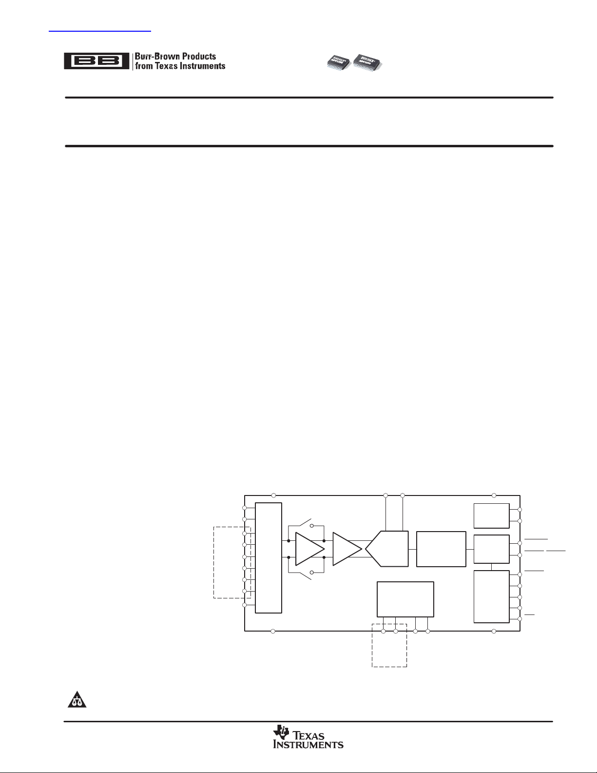
DESCRIPTION
The ADS1255 and ADS1256 are extremely low-noise,
24-bit analog-to-digital (A/D) converters. They provide
complete high-resolution measurement solutions for the
most demanding applications.
The converter is comprised of a 4th-order, delta-sigma
(∆Σ) modulator followed by a programmable digital filter. A
flexible input multiplexer handles differential or
single-ended signals and includes circuitry to verify the
integrity of the external sensor connected to the inputs.
The selectable input buffer greatly increases the input
impedance and the low-noise programmable gain
amplifier (PGA) provides gains from 1 to 64 in binary steps.
The programmable filter allows the user to optimize
between a resolution of up to 23 bits noise-free and a data
rate of up to 30k samples per second (SPS). The
converters offer fast channel cycling for measuring
multiplexed inputs and can also perform one-shot
conversions that settle in just a single cycle.
Communication is handled over an SPI-compatible serial
interface that can operate with a 2-wire connection.
Onboard calibration supports both self and system
correction of o ffset and gain errors for all the PGA settings.
Bidirectional digital I/Os and a programmable clock output
driver are provided for general use. The ADS1255 is
packaged in an SSOP-20, and the ADS1256 in an
SSOP-28.
VREFP VREFN
Clock
Generator
1:64
Buffer
PGA
4th−Order
Modulator
General
Purpose
Digital I/O
Programmable
Digital Filter
Control
Serial
Interface
XTAL1/CLKIN
XTAL2
RESET
SYNC/PDWN
DRDY
SCLK
DIN
DOUT
CS
D3 D2 D1 D0/CLKOUTAGND
ADS1256
Only
semiconductor products and disclaimers thereto appears at the end of this data sheet.
All trademarks are the property of their respective owners.
!"#$! # %& '( % )(*' +, +('
'%& )'%' ) - & % #. $(& ++ ,
+(' )' + ' '(+ % )&,
www.ti.com
Copyright 2003−2004, Texas Instruments Incorporated
DGND
Page 2
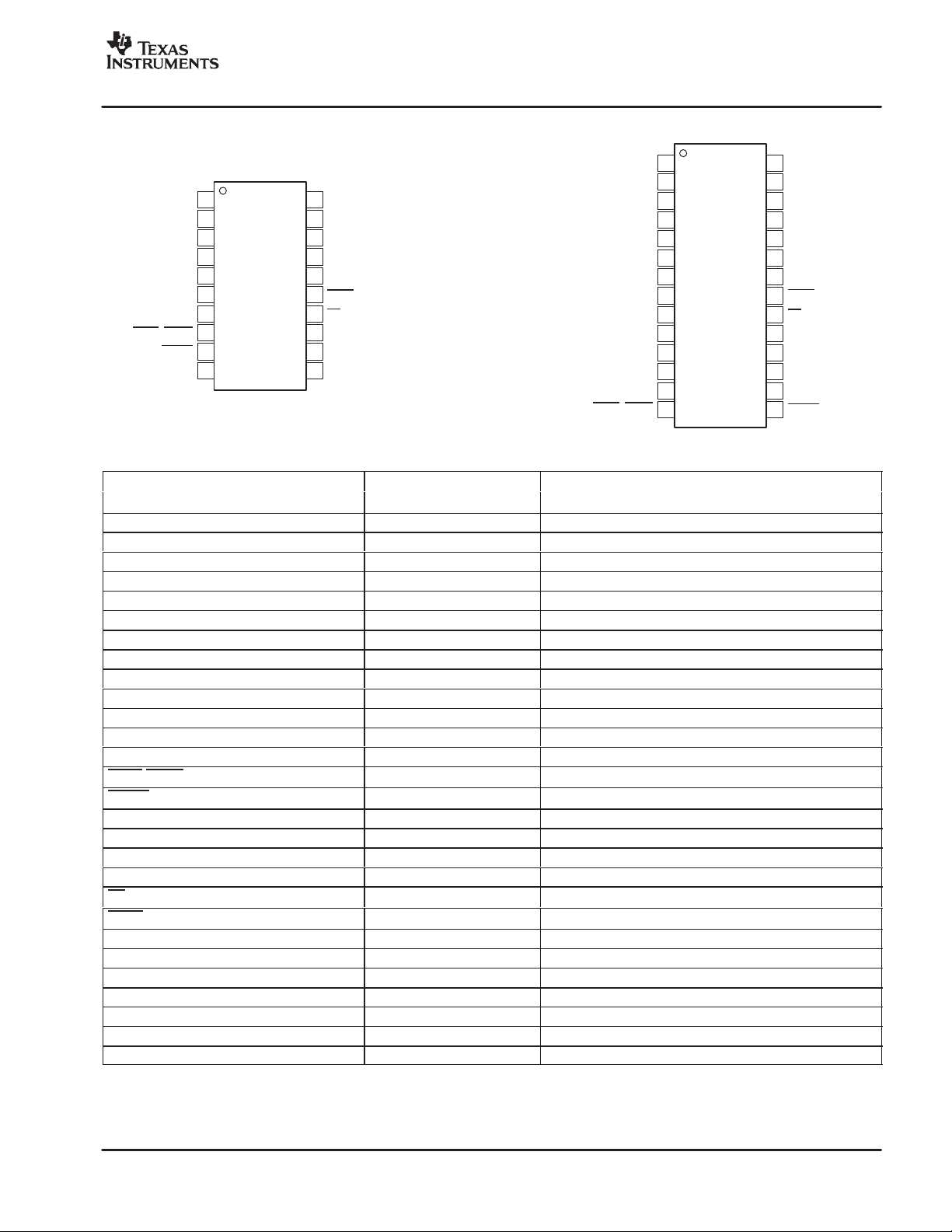
ADS1255
SSOP-20
DB
ADS1255IDB
ADS1256
SSOP-28
DB
ADS1256IDB
Input Current
l
inputs
SBAS288D − JUNE 2003 − REVISED AUGUST 2004
www.ti.com
ORDERING INFORMATION
PRODUCT PACKAGE-LEAD
(1)
For the most current package and ordering information, refer to our web site at www.ti.com.
(1)
PACKAGE
DESIGNATOR
PACKAGE
MARKING
ABSOLUTE MAXIMUM RATINGS
over operat i n g f ree-air temperature range unless otherwise noted
ADS1255, ADS1256 UNIT
AVDD to AGND −0.3 to +6 V
DVDD to DGND −0.3 to +3.6 V
AGND to DGND −0.3 to +0.3 V
100, Momentary mA
10, Continuous mA
Analog inputs to AGND −0.3 to AVDD + 0.3 V
DIN, SCLK, CS, RESET,
SYNC/PDWN,
Digita
XTAL1/CLKIN to DGND
D0/CLKOUT, D1, D2, D3
to DGND
Maximum Junction Temperature +150 °C
Operating Temperature Range −40 to +105 °C
Storage Temperature Range −60 to +150 °C
Lead Tem perature (soldering, 10s) +300 °C
(1)
Stresses above those listed under Absolute Maximum Ratings
may cause permanent damage to the device. Exposure to
absolute maximum conditions for extended periods may degrade
device reliability. These are stress ratings only, and functional
operation of the device at these or any other conditions beyond
those specified is not implied.
−0.3 to +6 V
−0.3 to DVDD + 0.3 V
(1)
proper handling and installation procedures can cause damage.
ESD damage can range from subtle performance degradation to
complete device failure. Precision integrated circuits may be more
susceptible t o damage because very small parametric changes could
cause the device not to meet its published specifications.
ORDERING NUMBER
ADS1255IDBT Tape and Reel, 250
ADS1255IDBR Tape and Reel, 1000
ADS1256IDBT Tape and Reel, 250
ADS1256IDBR Tape and Reel, 1000
This integrated circuit can be damaged by ESD. Texas
Instruments recommends that all integrated circuits be
handled with appropriate precautions. Failure to observe
TRANSPORT MEDIA,
QUANTITY
2
Page 3
Absolute input voltage
Differential input impedance
Sensor detect current sources
Integral nonlinearity
Offset drift
Gain error
Gain drift
Negative reference input (VREFN)
Positive reference input (VREFP)
IH
V
IH
Master clock rate
www.ti.com
SBAS288D − JUNE 2003 − REVISED AUGUST 2004
ELECTRICAL CHARACTERISTICS
All specifications at −40°C to +85°C, AVDD = +5V, DVDD = +1.8V, f
PARAMETER TEST CONDITIONS MIN TYP MAX UNIT
Analog Inputs
Full-scale input voltage (AINP − AINN) ±2V
Absolute input voltage
(AIN0-7, AINCOM to AGND)
Programmable gain amplifier 1 64
Differential input impedance
Sensor detect current sources
System Performance
Resolution 24 Bit
No missing codes All data rates and PGA settings 24 Bit
Data rate (f
Offset error After calibration On the level of the noise
Common-mode rejection f
Noise See Noise Performance Tables
AVDD power-supply rejection ±5% ∆ in AVDD 60 70 dB
DVDD power-supply rejection ±10% ∆ in DVDD 100 dB
Voltage Reference Inputs
Reference input voltage (V
Voltage reference impedance f
Digital Input/Output
V
V
IL
V
OH
V
OL
Input hysteresis 0.5 V
Input leakage 0 < V
Master clock rate
) f
DATA
REF
) V
Buffer off AGND − 0.1 AVDD + 0.1 V
Buffer on AGND AVDD − 2.0 V
Buffer off, PGA = 1, 2, 4, 8, 16 150/PGA kΩ
Buffer off, PGA = 32, 64 4.7 kΩ
Buffer on, f
SDCS[1:0] = 01 0.5 µA
SDCS[1:0] = 10 2 µA
SDCS[1:0] = 11 10 µA
= 7.68MHz 2.5 30,000 SPS
CLKIN
Differential input, PGA = 1 ±0.0003 ±0.0010 %FSR
Differential input, PGA = 64 ±0.0007 %FSR
PGA = 1 ±100 nV/°C
PGA = 64 ±4 nV/°C
After calibration, PGA = 1, Buffer on ±0.005 %
After calibration, PGA = 64, Buffer on ±0.03 %
PGA = 1 ±0.8 ppm/°C
PGA = 64 ±0.8 ppm/°C
(4)
= 60Hz, f
CM
≡ VREFP − VREFN 0.5 2.5 2.6 V
REF
Buffer off AGND − 0.1 VREFP − 0.5 V
Buffer on
Buffer off VREFN + 0.5 AVDD + 0.1 V
Buffer on
= 7.68MHz 18.5 kΩ
CLKIN
DIN, SCLK, XTAL1/CLKIN,
SYNC/PDWN, CS, RESET
D0/CLKOUT, D1, D2, D3 0.8 DVDD DVDD V
IOH = 5mA 0.8 DVDD V
IOL = 5mA 0.2 DVDD V
DIGITAL INPUT
External crystal between XTAL1 and
XTAL2
External oscillator driving CLKIN 0.1 7.68 10 MHz
(6)
(6)
DATA
≤ 50Hz
DATA
< DVDD ±10 µA
= 7.68MHz, PGA = 1, and V
CLKIN
(1)
= 30kSPS
(5)
= +2.5V , unless otherwise noted.
REF
/PGA V
REF
80 MΩ
95 110 dB
AGND VREFP − 0.5 V
VREFN + 0.5 AVDD − 2.0 V
0.8 DVDD 5.25 V
DGND 0.2 DVDD V
2 7.68 10 MHz
(2)
(3)
3
Page 4
AVDD current
DVDD current
Power dissipation
www.ti.com
SBAS288D − JUNE 2003 − REVISED AUGUST 2004
ELECTRICAL CHARACTERISTICS (continued)
All specifications at −40°C to +85°C, AVDD = +5V, DVDD = +1.8V, f
PARAMETER UNITMAXTYPMINTEST CONDITIONS
Power-Supply
AVDD 4.75 5.25 V
DVDD 1.8 3.6 V
Power-down mode 2 µA
Standby mode 20 µA
Normal mode, PGA = 1, Buffer off 7 10 mA
Normal mode, PGA = 64, Buffer off 16 22 mA
Normal mode, PGA = 1, Buffer on 13 19 mA
Normal mode, PGA = 64, Buffer on 36 50 mA
Power-down mode 2 µA
Standby mode, CLKOUT off,
DVDD current
Power dissipation
Temperature Range
Specified −40 +85 °C
Operating −40 +105 °C
Storage −60 +150 °C
(1)
See text for more information on input impedance.
(2)
SPS = samples per second.
(3)
FSR = full-scale range = 4V
(4)
fCM is the frequency of the common-mode input signal.
(5)
Placing a notch of the digital filter at 60Hz (setting f
common-mode rejection of this frequency.
(6)
The reference input range with Buffer on is restricted only if self-calibration or gain self-calibration is to be used. If using system calibration or
writing calibration values directly to the registers, the entire Buffer off range can be used.
REF
DVDD = 3.3V
Normal mode, CLKOUT off,
DVDD = 3.3V
Normal mode, PGA = 1, Buffer off,
DVDD = 3.3V
Standby mode, DVDD = 3.3V 0.4 mW
/PGA.
= 60SPS, 30SPS, 15SPS, 10SPS, 5SPS, or 2.5SPS) will further improve the
DATA
= 7.68MHz, PGA = 1, and V
CLKIN
= +2.5V , unless otherwise noted.
REF
95 µA
0.9 2 mA
38 57 mW
4
Page 5
www.ti.com
ANALOG/DIGITAL
SBAS288D − JUNE 2003 − REVISED AUGUST 2004
PIN ASSIGNMENTS
AVDD
AGND
VREFN
VREFP
AINCOM
AIN0
AIN1
SYNC, PDWN
RESET
DVDD
SSOP P ACKAGE
(TOP VIEW)
1
2
3
4
5
ADS1255 ADS1256
6
7
8
9
10 11
D1
20
D0/CLKOUT
19
SCLK
18
DIN
17
DOUT
16
15
DRDY
CS
14
XTAL1/CLKIN
13
XTAL2
12
DGND
AVDD
AGND
VREFN
VREFP
AINCOM
AIN0
AIN1
AIN2
AIN3
AIN4
AIN5
AIN6
AIN7
SYNC, PDWN
1
2
3
4
5
6
7
8
9
10
11
12
13
14
Terminal Functions
TERMINAL NO.
NAME ADS1255 ADS1256
AVDD 1 1 Analog Analog power supply
AGND 2 2 Analog Analog ground
VREFN 3 3 Analog input Negative reference input
VREFP 4 4 Analog input Positive reference input
AINCOM 5 5 Analog input Analog input common
AIN0 6 6 Analog input Analog input 0
AIN1 7 7 Analog input Analog input 1
AIN2 — 8 Analog input Analog input 2
AIN3 — 9 Analog input Analog input 3
AIN4 — 10 Analog input Analog input 4
AIN5 — 11 Analog input Analog input 5
AIN6 — 12 Analog input Analog input 6
AIN7 — 13 Analog input Analog input 7
SYNC/PDWN 8 14 Digital input
RESET 9 15 Digital input
DVDD 10 16 Digital Digital power supply
DGND 11 17 Digital Digital ground
XTAL2 12 18 Digital
XTAL1/CLKIN 13 19 Digital/Digital input
CS 14 20 Digital input
DRDY 15 21 Digital output: active low Data ready output
DOUT 16 22 Digital output Serial data output
DIN 17 23 Digital input
SCLK 18 24 Digital input
D0/CLKOUT 19 25 Digital IO
D1 20 26 Digital IO
D2 — 27 Digita l IO
D3 — 28 Digita l IO
(1)
Schmitt-Trigger digital input.
(2)
5V tolerant digital input.
(3)
Leave disconnected if external clock input is applied to XTAL1/CLKIN.
(4)
Schmitt-Trigger digital input when the digital I/O is configured as an input.
INPUT/OUTPUT
(1)(2)
: active low Synchronization / power down input
(1)(2)
: active low Reset input
(3)
(1)(2)
: active low Chip select
(1)(2)
(1)(2)
(4)
(4)
(4)
(4)
(2)
Crystal oscillator connection
Crystal oscillator connection / external clock input
Serial data input
Serial clock input
Digital I/O 0 / clock output
Digital I/O 1
Digital I/O 2
Digital I/O 3
DESCRIPTION
D3
28
D2
27
D1
26
D0/CLKOUT
25
SCLK
24
DIN
23
DOUT
22
DRDY
21
20
CS
XTAL1/CLKIN
19
XTAL2
18
DGND
17
DVDD
16
RESET
15
5
Page 6
t
SCLK period
t
SCLK pulse width: high
Final SCLK falling edge of command to first SCLK
www.ti.com
SBAS288D − JUNE 2003 − REVISED AUGUST 2004
PARAMETER MEASUREMENT INFORMATION
CS
SCLK
DIN
DOUT
t
3
t
4
t
1
t
5
Figure 1. Serial Interface Timing
TIMING CHARACTERISTICS FOR FIGURE 1
SYMBOL DESCRIPTION MIN MAX UNIT
1
2H
t
2L
t
t
t
t
t
t
t
t
10
t
11
(1)
τ
CLKIN
(2)
τ
DATA
(3)
CS can be tied low.
(4)
DOUT load = 20pF 100kΩ to DGND.
SCLK pulse width: low
CS low to first SCLK: setup time
3
Valid DIN to SCLK falling edge: setup time
4
Valid DIN to SCLK falling edge: hold time
5
Delay from last SCLK edge for DIN to first SCLK rising edge for DOUT: RDATA, RDATAC,
6
RREG Commands
SCLK rising edge to valid new DOUT: propagation delay
7
SCLK rising edge to DOUT invalid: hold time
8
Last SCLK falling edge to DOUT high impedance
9
NOTE: DOUT goes high impedance immediately when CS goes high
(3)
CS low after final SCLK falling edge
RREG, WREG, RDATA
RDATAC, RESET, SYNC
rising edge of next command.
RDATAC, STANDBY, SELFOCAL, SYSOCAL, SELFGCAL,
SYSGCAL, SELFCAL
= master clock period = 1/f
= output data period 1/f
DATA
CLKIN
.
.
(4)
t
2H
t
6
t
7
t
2L
t
8
t
10
t
11
t
9
4 τ
10 τ
CLKIN
DATA
200 ns
9 τ
200 ns
0 ns
50 ns
50 ns
50 τ
50 ns
0 ns
6 10 τ
0 ns
4 τ
24 τ
Wait for DRDY to go low
(1)
(2)
DATA
CLKIN
CLKIN
CLKIN
CLKIN
6
Page 7
www.ti.com
SBAS288D − JUNE 2003 − REVISED AUGUST 2004
SCLK
t
13
t
12
t
13
t
14
t
15
Figure 2. SCLK Reset Timing
TIMING CHARACTERISTICS FOR FIGURE 2
SYMBOL DESCRIPTION MIN MAX UNIT
(1)
t
12
t
13
t
14
t
15
τ
CLKIN
SCLK reset pattern, first high pulse
SCLK reset pattern, low pulse
SCLK reset pattern, second high pulse
SCLK reset pattern, third high pulse
= master clock period = 1/f
CLKIN
.
t
16
RESET, SYNC/PDWN
300 500 τ
5 τ
550 750 τ
1050 1250 τ
CLKIN
Figure 3. RESET and SYNC/PDWN Timing
TIMING CHARACTERISTICS FOR FIGURE 3
SYMBOL DESCRIPTION MIN MAX UNIT
(1)
t
16
τ
CLKIN
RESET, SYNC/PDWN, pulse width
= master clock period = 1/f
CLKIN
.
4 τ
CLKIN
(1)
CLKIN
CLKIN
CLKIN
(1)
t
17
DRDY
Figure 4. DRDY Update Timing
TIMING CHARACTERISTICS FOR FIGURE 4
SYMBOL DESCRIPTION MIN MAX UNIT
(1)
t
17
τ
CLKIN
Conversion data invalid while being updated (DRDY shown with no data retrieval)
= master clock period = 1/f
CLKIN
.
16 τ
CLKIN
(1)
7
Page 8
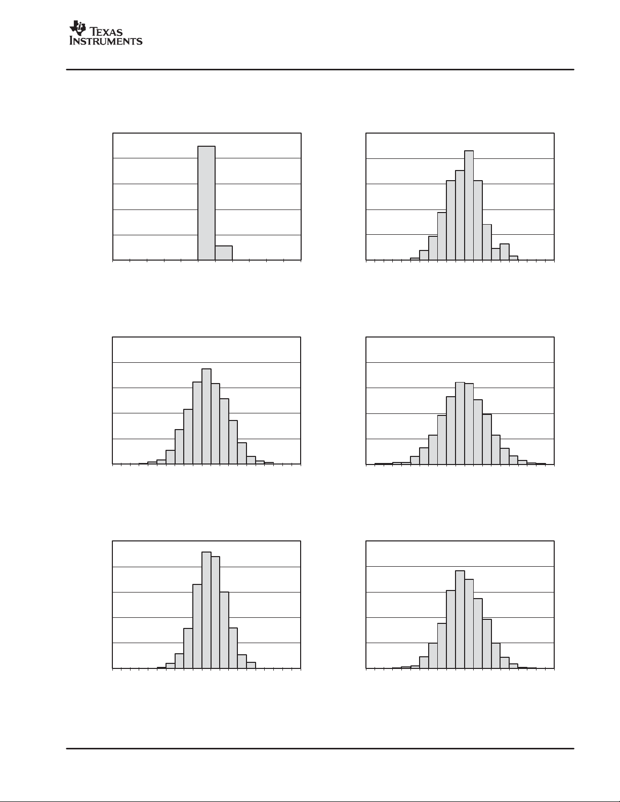
OFFSET DRIFT HISTOGRAM
OFFSET DRIFT HISTOGRAM
GAIN ERROR HISTOGRAM
GAIN ERROR HISTOGRAM
GAIN DRIFT HISTOGRAM
GAIN DRIFT HISTOGRAM
SBAS288D − JUNE 2003 − REVISED AUGUST 2004
TYPICAL CHARACTERISTICS
TA = +25°C, AVDD = 5V, DVDD = 1.8V, f
CLKIN
= 7.68MHz, PGA = 1, and V
= 2.5V , unless otherwise noted.
REF
www.ti.com
25
PGA = 1 90 Units from 3 Production Lots
20
15
10
Percent of Population
5
0
500−450−400−350−300−250−200−150−100
−
30
PGA = 1
25
20
15
10
Percent of Population
5
Offset Drift (nV/_C)
0
50
50
−
100
150
200
90 Units from 3 Production Lots
30
PGA = 64
25
20
15
10
Percent of Population
5
0
10
25
20
15
10
Percent of Population
5
−20−18−16−14−12−
PGA = 64
250
300
350
400
450
500
90 Units from 3 Production Lots
2
−8−6−4−
Offset Drift (nV/_C)
02468
90 Units from 3 Production Lots
1012141618
20
0
0.0100−0.0095−0.0090−0.0085−0.0080−0.0075−0.0070−0.0065−0.0060−0.0055−0.0050−0.0045−0.0040−0.0035−0.0030−0.0025−0.0020−0.0015−0.0010−0.0005
−
25
PGA = 1
20
15
10
Percent of Population
5
0
0
0.1
0.2
0.3
Gain Error (%)
0.4
0.5
0.6
0.7
GainDrift (ppm/_C)
90 Units from 3 Production Lots
0.8
0.9
1.0
1.1
1.2
0
1.3
1.4
1.5
1.6
1.7
1.8
1.9
2.0
0
0.060−0.057−0.054−0.051−0.048−0.045−0.042−0.039−0.036−0.033−0.030−0.027−0.024−0.021−0.018−0.015−0.012−0.009−0.006−0.003
Percent of Population
25
20
15
10
5
0
−
PGA = 64
0
0.1
0.2
0.3
Gain Error (%)
0.4
0.5
0.6
0.7
GainDrift (ppm/_C)
90 Units from 3 Production Lots
0.8
0.9
1.0
1.1
1.2
0
1.3
1.4
1.5
1.6
1.7
1.8
1.9
2.0
8
Page 9
www.ti.com
NOISE HISTOGRAM
NOISE HISTOGRAM
NOISE HISTOGRAM
NOISE HISTOGRAM
NOISE HISTOGRAM
NOISE HISTOGRAM
TYPICAL CHARACTERISTICS (continued)
TA = +25°C, AVDD = 5V, DVDD = 1.8V, f
= 7.68MHz, PGA = 1, and V
CLKIN
SBAS288D − JUNE 2003 − REVISED AUGUST 2004
= 2.5V , unless otherwise noted.
REF
100
PGA = 1
Data Rate = 2.5SPS
80
60
40
Percent of Population
20
0
−5−4−3−2−
25
PGA = 1
Data Rate = 1kSPS
20
15
10
Buffer= Off
256 Readings
10 1 2 3 4 5
Output Code (LSB)
Buffer = Off
4096 Readings
25
PGA = 64
Data Rate = 2.5SPS
20
15
10
Percent of Population
5
0
−20−18−16−14−12−
25
PGA = 64
Data Rate = 1kSPS
20
15
10
10
2
−8−6−4−
Output Code(LSB)
02468
Buffer = Off
256 Readings
1012141618
Buffer = Off
4096Readings
20
Percent of Population
5
0
−20−18−16−14−12−
25
PGA = 1
DataRate= 30kSPS
20
15
10
Percent of Population
5
0
100
−90−80−70−60−50−40−30−20−
−
10
2
−8−6−4−
Output Code(LSB)
10
Output Code(LSB)
02468
0
102030405060708090
1012141618
Buffer = Off
4096 Readings
20
100
Percent of Population
5
0
150−135−120−105
−
25
PGA = 64
Data Rate = 30kSPS
20
15
10
Percent of Population
5
0
600−540−480−420−360−300−240−180−120
−
−90−75−60−45−30−
Output Code(LSB)
Output Code(LSB)
15
60
−
0
0
1530456075
4096 Readings
60
120
180
240
90
105
Buffer = Off
300
360
420
120
480
135
540
150
600
9
Page 10
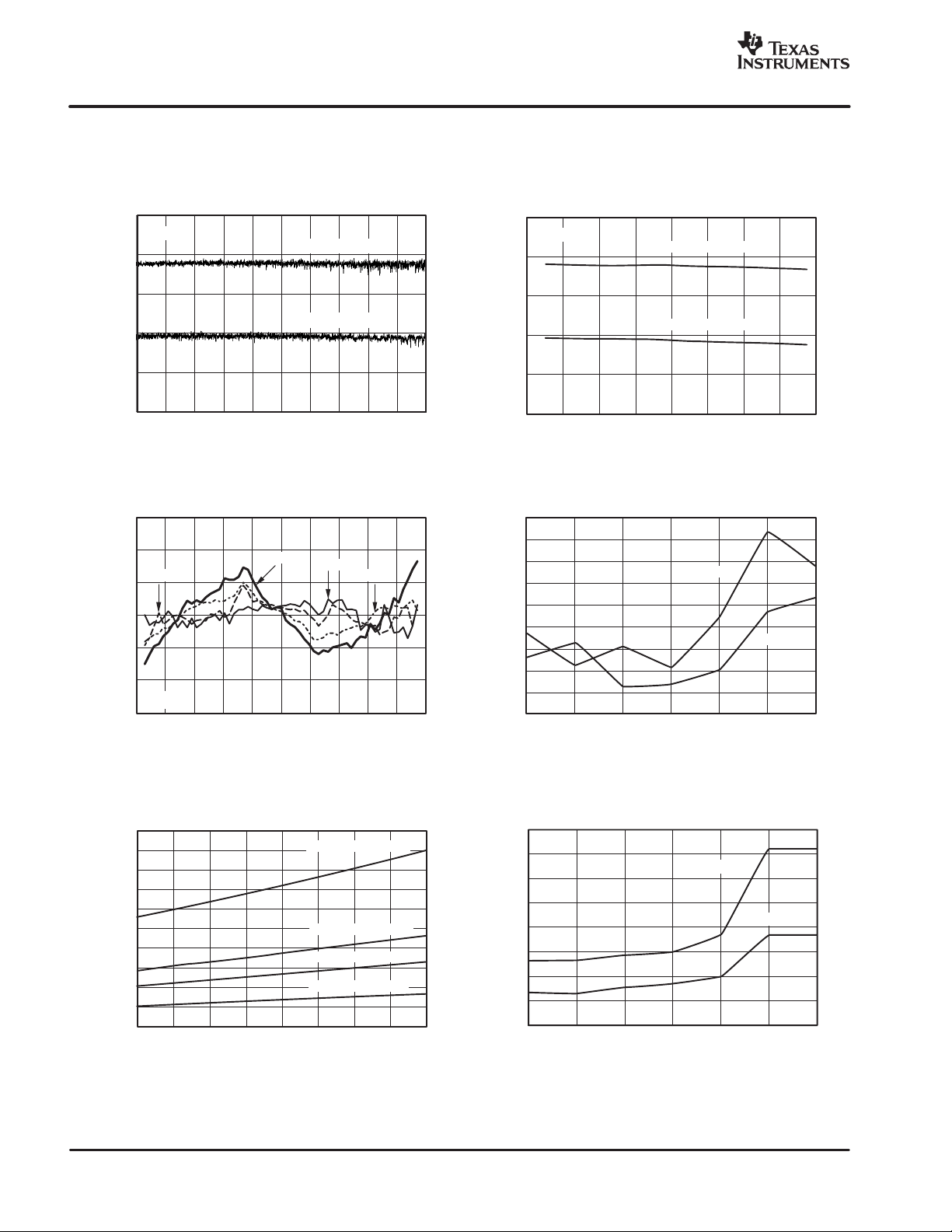
EFFECTIVE NUMBER OF BITS
EFFECTIVE NUMBEROF BITS
INTEGRAL NONLINEARITY vs INPUT SIGNAL
INL (% of FSR)
INTEGRAL NONLINEARITY vs PGA
ANALOG SUPPLY CURRENT vs TEMPERATURE
ANALOG SUPPLY CURRENT vs PGA
SBAS288D − JUNE 2003 − REVISED AUGUST 2004
TYPICAL CHARACTERISTICS (continued)
TA = +25°C, AVDD = 5V, DVDD = 1.8V, f
= 7.68MHz, PGA = 1, and V
CLKIN
= 2.5V , unless otherwise noted.
REF
www.ti.com
0.0006
0.0004
0.0002
−
0.0002
−
0.0004
−
0.0006
23
PGA = 1
22
21
20
ENOB(rms)
19
18
0
PGA = 1
−4−
−
5
vs INPUT VOLTAGE
Input Voltage, V
−2−
3
Input Voltage, VIN(V)
Data Rate = 1kSPS
Data Rate = 30kSPS
2.50 0.5 1.0 1.5 2.0 3.0 3.5 4.0 4.5 5.0
(V)
IN
−40_
C
+125_C
+25_C+85_C
1345210
0.0009
0.0008
0.0007
0.0006
0.0005
(% of FSR)
0.0004
INL
0.0003
0.0002
0.0001
23
PGA = 1
22
21
20
ENOB (rms)
19
18
−
−
30
50
0
2148 643216
vs TEMPERATURE
Data Rate = 1kSPS
Data Rate = 30kSPS
−
10 10 30 90 1107050
Temperature(_C)
PGA Setting
Buffer Off
Buffer On
50
45
40
35
30
25
20
15
Analog Current (mA)
10
5
0
−
−
50
−
30
10 10 30 90 1107050
Temperature(_C)
PGA = 64, Buffer On
PGA = 64, Buffer Off
PGA = 1, Buffer On
PGA = 1, Buffer Off
40
35
30
25
20
15
Analog Current (mA)
10
5
0
2148 643216
PGA Setting
Buffer On
Buffer Off
10
Page 11
www.ti.com
SBAS288D − JUNE 2003 − REVISED AUGUST 2004
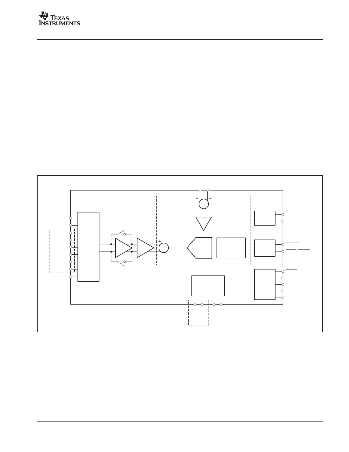
OVERVIEW
The ADS1255 and ADS1256 are very low-noise A/D
converters. The ADS1255 supports one differential or two
single-ended inputs and has two general-purpose digital
I/Os. The ADS1256 supports four differential or eight
single-ended inputs and has four general-purpose digital
I/Os. Otherwise, the two units are identical and are
referred to together in this data sheet as the ADS1255/6.
Figure 5 shows a block diagram of the ADS1256. The
input multiplexer selects which input pins are connected to
the A/D converter. Selectable current sources within the
input multiplexer can check for open- or short-circuit
conditions on the external sensor. A selectable onboard
input buffer greatly reduces the input circuitry loading by
providing up to 80MΩ of impedance. A low-noise PGA
provides a gain of 1, 2, 4, 8, 16, 32, or 64. The ADS1255/6
converter is comprised of a 4th-order, delta-sigma
modulator followed by a programmable digital filter.
AIN0
AIN1
AIN2
AIN3
AIN4
AIN5
AIN6
ADS1256 Only
AIN7
AINCOM
Input
Multiplexer
and
Sensor
Detect
AIN
AIN
P
Buffer
N
PGA
1:64
Σ
The modulator measures the amplified differential input
signal, V
reference, V
= (AINP – AINN), against the differential
IN
= (VREFP − VREFN). The differential
REF
reference is scaled internally by a factor of two so that the
full-scale input range is ±2V
(for PGA = 1).
REF
The digital filter receives the modulator signal and
provides a low-noise digital output. The data rate of the
filter is programmable from 2.5SPS to 30kSPS and allows
tradeoffs between resolution and speed.
Communication is done over an SPI-compatible serial
interface with a set of simple commands providing control of
the ADS1255/6. Onboard registers store t he v arious settings
for the input m ultiplexer , s ensor detect current sources, input
buffer enable, PGA setting, data rate, etc. Either an external
crystal or clock oscillator can be used to provide the clock
source. General-purpose digital I /Os p rovide static r ead/write
control of up to four pins. One of the pins can also be used
to supply a programmable clock output.
VREFP VREFN
Σ
V
REF
2
2V
REF
•
V
PGA
IN
4th−Order
Modulator
General
Purpose
Digital I/O
A/D
Converter
Programmable
Digital Filter
Clock
Generator
Control
SPI
Serial
Interface
XTAL1/CLKIN
XTAL2
RESET
SYNC/PDWN
DRDY
SCLK
DIN
DOUT
CS
D3 D2 D1 D0/CLKOUT
ADS1256
Only
Figure 5. Block Diagram
11
Page 12
RATE
RATE
RATE
SBAS288D − JUNE 2003 − REVISED AUGUST 2004
www.ti.com
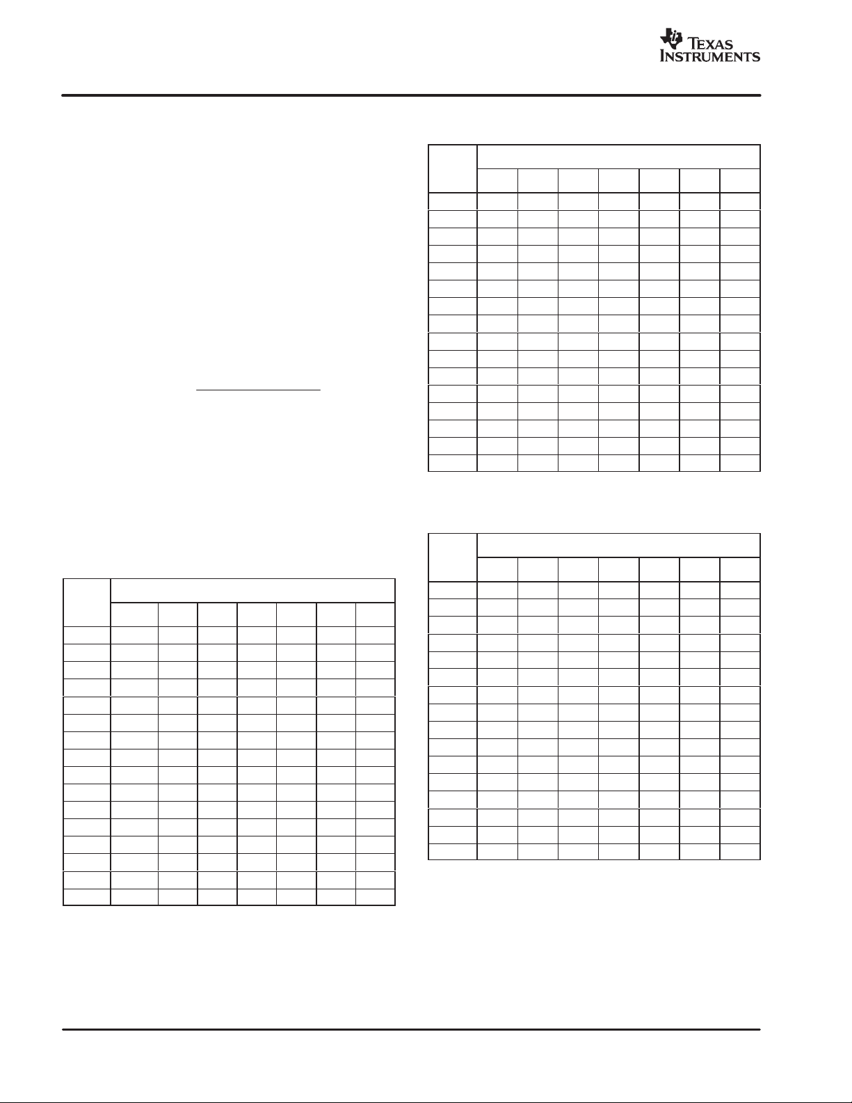
NOISE PERFORMANCE
The ADS1255/6 offer outstanding noise performance that
can be optimized by adjusting the data rate or PGA setting.
As the averaging is increased by reducing the data rate,
the noise drops correspondingly. The PGA reduces the
input-referred noise when measuring lower level signals.
Table 1 through Table 6 summarize the typical noise
performance with the inputs shorted externally. In all six
tables, the following conditions apply: T = +25°C,
AVDD = 5V, DVDD = 1.8V, V
7.68MHz. Table 1 to Table 3 reflect the device input bu ffer
enabled. Table 1 shows the rms value of the input-referred
noise in volts. Table 2 shows the effective number of bits
of resolution (ENOB), using the noise data from Table 1.
ENOB is defined as:
ENOB +
lnǒFSRńRMS Noise
where FSR is the full-scale range. Table 3 shows the
noise-free bits of resolution. It is calculated with the same
formula as ENOB except the peak-to-peak noise value is
used instead of rms noise. Table 4 through Table 6 show
the same noise data, but with the input buffer disabled.
= 2.5V, and f
REF
)
ln(2
=
CLKIN
Ǔ
Table 2. Effective Number of Bits (ENOB, rms)
with Buffer On
DATA
(SPS)
2.5 25.3 24.9 24.9 24.4 23.8 23.0 22.2
5 25.0 24.8 24.5 24.0 23.3 22.7 21.8
10 24.8 24.5 24.1 23.5 22.9 22.3 21.3
15 24.6 24.2 23.8 23.2 22.5 21.8 21.0
25 24.3 24.0 23.4 23.0 22.2 21.5 20.7
30 24.2 23.8 23.3 22.8 22.1 21.5 20.5
50 23.9 23.6 23.0 22.5 21.8 21.1 20.3
60 23.8 23.4 22.9 22.4 21.7 21.0 20.2
100 23.4 23.0 22.5 22.0 21.4 20.8 19.8
500 22.3 21.9 21.5 20.9 20.3 19.6 18.7
1000 21.7 21.3 20.8 20.2 19.8 19.2 18.3
2000 21.2 20.9 20.4 19.7 19.3 18.8 17.9
3750 20.8 20.5 20.0 19.4 19.0 18.4 17.4
7500 20.4 20.1 19.6 19.0 18.5 17.9 17.0
15,000 20.1 19.7 19.3 18.7 18.2 17.7 16.7
30,000 19.8 19.5 19.1 18.5 18.0 17.4 16.5
1 2 4 8 16 32 64
PGA
Table 3. Noise-Free Resolution (bits)
with Buffer On
Table 1. Input Referred Noise (µV, rms)
with Buffer On
DATA
(SPS)
2.5 0.247 0.156 0.080 0.056 0.043 0.037 0.033
5 0.301 0.175 0.102 0.076 0.061 0.045 0.044
10 0.339 0.214 0.138 0.106 0.082 0.061 0.061
15 0.401 0.264 0.169 0.126 0.107 0.085 0.073
25 0.494 0.305 0.224 0.149 0.134 0.102 0.093
30 0.533 0.335 0.245 0.176 0.138 0.104 0.106
50 0.629 0.393 0.292 0.216 0.168 0.136 0.122
60 0.692 0.438 0.321 0.233 0.184 0.146 0.131
100 0.875 0.589 0.409 0.305 0.229 0.170 0.169
500 1.946 1.250 0.630 0.648 0.497 0.390 0.367
1000 2.931 1.891 1.325 1.070 0.689 0.512 0.486
2000 4.173 2.589 1.827 1.492 0.943 0.692 0.654
3750 5.394 3.460 2.376 1.865 1.224 0.912 0.906
7500 7.249 4.593 3.149 2.436 1.691 1.234 1.187
15,000 9.074 5.921 3.961 2.984 2.125 1.517 1.515
30,000 10.728 6.705 4.446 3.280 2.416 1.785 1.742
1 2 4 8 16 32 64
PGA
DATA
(SPS)
2.5 23.0 22.6 22.1 21.7 21.3 20.8 19.7
5 22.3 22.4 21.9 21.3 20.7 20.3 19.3
10 22.3 22.0 21.6 21.0 20.4 19.9 18.9
15 22.0 21.7 21.3 20.7 20.1 19.3 18.7
25 21.7 21.4 21.1 20.5 19.7 19.2 18.5
30 21.8 21.3 20.8 20.4 19.8 19.0 18.1
50 21.3 21.1 20.4 19.9 19.4 18.8 17.9
60 21.3 20.9 20.5 19.8 19.3 18.8 17.8
100 20.9 20.7 20.2 19.6 19.1 18.5 17.4
500 20.1 19.6 19.1 18.6 18.0 17.3 16.3
1000 19.0 18.6 18.1 17.5 17.2 16.5 15.6
2000 18.5 18.1 17.8 17.0 16.6 16.1 15.3
3750 18.1 17.8 17.3 16.6 16.2 15.7 14.7
7500 17.7 17.3 16.9 16.2 15.8 15.3 14.4
15,000 17.3 17.0 16.5 15.9 15.5 14.9 13.9
30,000 17.1 16.7 16.4 15.9 15.4 14.6 13.8
1 2 4 8 16 32 64
PGA
12
Page 13

www.ti.com
RATE
RATE
RATE
SBAS288D − JUNE 2003 − REVISED AUGUST 2004
Table 4. Input Referred Noise (µV, rms)
with Buffer Off
DATA
(SPS)
2.5 0.247 0.149 0.097 0.058 0.036 0.031 0.027
5 0.275 0.176 0.109 0.070 0.046 0.039 0.038
10 0.338 0.201 0.129 0.084 0.063 0.048 0.047
15 0.401 0.221 0.150 0.109 0.070 0.063 0.057
25 0.485 0.279 0.177 0.136 0.093 0.076 0.076
30 0.559 0.315 0.202 0.142 0.107 0.093 0.082
50 0.644 0.390 0.238 0.187 0.129 0.108 0.103
60 0.688 0.417 0.281 0.204 0.134 0.109 0.111
100 0.815 0.530 0.360 0.233 0.169 0.123 0.122
500 1.957 1.148 0.772 0.531 0.375 0.276 0.259
1000 2.803 1.797 1.191 0.940 0.518 0.392 0.365
2000 4.025 2.444 1.615 1.310 0.700 0.526 0.461
3750 5.413 3.250 2.061 1.578 0.914 0.693 0.625
7500 7.017 4.143 2.722 1.998 1.241 0.914 0.857
15,000 8.862 5.432 3.378 2.411 1.569 1.149 1.051
30,000 10.341 6.137 3.873 2.775 1.805 1.313 1.211
1 2 4 8 16 32 64
PGA
Table 5. Effective Number of Bits (ENOB, rms)
with Buffer Off
Table 6. Noise-Free Resolution (bits)
with Buffer Off
DATA
(SPS)
2.5 23.0 22.4 22.0 21.9 21.3 21.1 20.0
5 22.4 22.1 21.9 21.5 21.2 20.4 19.4
10 22.3 22.1 21.7 21.5 20.8 20.3 19.2
15 22.0 21.8 21.4 20.8 20.6 19.9 19.0
25 21.8 21.7 21.1 20.7 20.3 19.5 18.6
30 21.6 21.4 21.1 20.4 20.0 16.4 18.5
50 21.3 21.3 20.7 20.1 19.8 19.1 18.2
60 21.2 21.0 20.6 20.1 19.8 19.1 18.1
100 21.1 20.5 20.3 19.9 19.5 19.0 17.9
500 20.0 19.7 19.3 18.9 18.3 17.8 16.9
1000 19.0 18.7 18.4 17.7 17.5 16.9 15.9
2000 18.5 18.3 17.9 17.4 17.0 16.4 15.6
3750 18.1 17.8 17.5 17.0 16.7 16.1 15.2
7500 17.7 17.6 17.0 16.6 16.2 15.7 14.8
15,000 17.4 17.1 16.8 16.3 15.9 15.3 14.4
30,000 17.1 17.0 16.6 16.0 15.6 15.0 14.4
1 2 4 8 16 32 64
PGA
DATA
(SPS)
2.5 25.3 25.0 24.6 24.4 24.0 23.2 22.5
5 25.1 24.8 24.5 24.1 23.7 22.9 22.0
10 24.8 24.6 24.2 23.8 23.2 22.6 21.7
15 24.6 24.4 24.0 23.4 23.1 22.2 21.4
25 24.3 24.1 23.8 23.1 22.7 22.0 21.0
30 24.1 23.9 23.6 23.1 22.5 21.7 20.9
50 23.9 23.6 23.3 22.7 22.2 21.5 20.5
60 23.8 23.5 23.1 22.5 22.1 21.5 20.4
100 23.5 23.2 22.7 22.4 21.8 21.3 20.3
500 22.3 22.1 21.6 21.2 20.7 20.1 19.2
1000 21.8 21.4 21.0 20.3 20.2 19.6 18.7
2000 21.2 21.0 20.6 19.9 19.8 19.2 18.4
3750 20.8 20.6 20.2 19.6 19.4 18.8 17.9
7500 20.4 20.2 19.8 19.3 18.9 18.4 17.5
15,000 20.1 19.8 19.5 19.0 18.6 18.1 17.2
30,000 19.9 19.6 19.3 18.8 18.4 17.9 17.0
1 2 4 8 16 32 64
PGA
13
Page 14

SBAS288D − JUNE 2003 − REVISED AUGUST 2004
www.ti.com
INPUT MULTIPLEXER
Figure 6 shows a simplified diagram of the input
multiplexer. This flexible block allows any analog input pin
to be connected to either of the converter differential
inputs. That is, any pin can be selected as the positive
input (AIN
negative input (AIN
); likewise, any pin can be selected as the
P
). The pin selection is controlled by
N
the multiplexer register.
The ADS1256 offers nine analog inputs, which can be
configured as four independent differential inputs, eight
single-ended inputs, or a combination of differential and
single-ended inputs.
The ADS1255 offers three analog inputs, which can be
configured as one differential input or two single-ended
inputs. When using the ADS1255 and programming the
input, make sure to select only the available inputs when
programming the input multiplexer register.
In general, there are no restrictions on input pin selection.
AVDD
AIN0
AVDD
However, for optimum analog performance, the following
recommendations are made:
1. For differential measurements use AIN0 through
AIN7, preferably adjacent inputs. For example, use
AIN0 and AIN1. Do not use AINCOM.
2. For single-ended measurements use AINCOM as
common input and AIN0 through AIN7 as
single-ended inputs.
3. Leave any unused analog inputs floating. This
minimizes the input leakage current.
ESD diodes protect the analog inputs. To keep these
diodes from turning on, make sure the voltages on the
input pins do not go below AGND by more than 100mV,
and likewise do not exceed AVDD by more than 100mV:
−100mV < (AIN0 − 7 and AINCOM) < AVDD + 100mV.
When using ADS1255/6 for single-ended measurements,
it is important to note that common input AINCOM does not
need to be tied to ground. For example, AINCOM can be
tied to a midpoint reference such as +2.5V or even AVDD.
AIN1
AIN2
AIN3
AIN4
AIN5
AIN6
AIN7
AINCOM
AVDD
AVDD
AVDD
AVDD
AVDD
AVDD
ADS1256 Only
AVDD AGND
InputMultiplexer
AVDD
AIN
AIN
AGND
Sensor Detect
Current
Source
P
Input
Buffer
N
Sensor Detect
Current
Source
14
Figure 6. Simplified Diagram of the Input Multiplexer
Page 15

www.ti.com
SBAS288D − JUNE 2003 − REVISED AUGUST 2004
OPEN/SHORT SENSOR DETECTION
The sensor detect current sources (SDCS) provide a
means to verify the integrity of the external sensor
connected to the ADS1255/6. When enabled, the SDCS
supply a current (I
) of approximately 0.5µA, 2µA, or
SDC
10µA to the sensor through the input multiplexer. The
SDCS bits in the ADCON register enable the SDCS and
set the value of I
SDC
.
When the SDCS are enabled, the ADS1255/6
automatically turns on the analog input buffer regardless
of the BUFEN bit setting. This is done to prevent the input
circuitry from loading the SDCS. AIN
must stay below 3V
P
to be within the absolute input range of the buffer. To
ensure this condition is met, a 3V clamp will start sinking
current from AIN
to AGND if AINP exceeds 3V. Note that
P
this clamp is activated only when the SDCS are enabled.
Figure 7 shows a simplified diagram of ADS1255/6 input
structure with the external sensor modeled as resistance
R
between two input pins. When the SDCS are
SENS
enabled, they source I
AIN
and sink I
P
SDC
The two 25Ω series resistors, R
to the input pin connected to
SDC
from the input pin connected to AINN.
model the
MUX,
ADS1255/6 internal resistances. The signal measured
with the SDCS enabled equals the total IR drop:
I
× (2R
SDC
direct short (that is, R
MUX
+ R
). Note that when the sensor is a
SENS
= 0), there will still be a small
SENS
signal measured by the ADS1255/6 when the SDCS are
enabled: I
SDC
× 2R
MUX
.
ANALOG INPUT BUFFER
To dramatically increase the input impedance presented
by the ADS1255/6, the low-drift chopper-stabilized buffer
can be enabled via the BUFEN bit in the STA TUS register.
The input impedance with the buffer enabled can be
modeled by a resistor, as shown in Figure 8. Table 7 lists
the values of Z
for the different data rate settings. The
EFF
input impedance scales inversely with the frequency of
CLKIN. For example, if f
3.84MHz, Z
for a data rate of 50SPS will double from
EFF
is reduced by half to
CLKIN
80MΩ to 160MΩ.
AIN0
AIN1
AIN2
AIN3
AIN4
AIN5
AIN6
ADS1256 Only
AIN7
AINCOM
Input
Multiplexer
AIN
AIN
P
Z
EFF
N
Figure 8. Effective Impedance with Buffer On
AVDD
Sensor Detect
Current Source
R
MUX
Ω
25
AIN
P
3V
R
SENS
R
MUX
25
NOTE: Arrows indicate switch positions when the SDCS are enabled.
Clamp
Ω
AIN
N
Sensor Detect
Current Source
Input
Buffer
Figure 7. Sensor Detect Circuitry
Table 7. Input Impedance with Buffer On
NOTE: f
DATA RATE
(SPS)
30,000 10
15,000 10
7,500 10
3,750 10
2,000 10
1,000 20
500 40
100 40
60 40
≤ 50 80
= 7.68MHz.
CLKIN
Z
EFF
(MΩ)
With the buffer enabled, the voltage on the analog inputs
with respect to ground (listed in the Electrical
Characteristics as Absolute Input Voltage) must remain
between AGND and AVDD − 2.0V. Exceeding this range
reduces performance, in particular the linearity of the
ADS1255/6. This same voltage range, AGND to
AVDD − 2.0V, applies to the reference inputs when
performing a self gain calibration with the buffer enabled.
15
Page 16

SBAS288D − JUNE 2003 − REVISED AUGUST 2004
www.ti.com
PROGRAMMABLE GAIN AMPLIFIER (PGA)
The ADS1255/6 is a very high resolution converter. To
further complement its performance, the low-noise PGA
provides even more resolution when measuring smaller
input signals. For the best resolution, set the PGA to the
highest possible setting. This will depend on the largest
input signal to be measured. The ADS1255/6 full-scale
input voltage equals ±2V
/PGA. Table 8 shows the
REF
full-scale input voltage for the different PGA settings for
V
= 2.5V. For example, if the largest signal to be
REF
measured is 1.0V, the optimum PGA setting would be 4,
which gives a full-scale input voltage of 1.25V. Higher
PGAs cannot be used since they cannot handle a 1.0V
input signal.
Table 8. Full-Scale Input Voltage vs
PGA Setting
PGA SETTING FULL-SCALE INPUT VOLTAGE (V
1 ±5V
2 ±2.5V
4 ±1.25V
8 ±0.625V
16 ±312.5mV
32 ±156.25mV
64 ±78.125mV
REF
= 2.5V)
The PGA is controlled by the ADCON register.
Recalibrating the A/D converter after changing the PGA
setting is recommended. The time required for
self-calibration is dependent on the PGA setting. See the
Calibration section for more details. The analog current
and input impedance (when the buffer is disabled) vary as
a function of PGA setting.
MODULATOR INPUT CIRCUITRY
The ADS1255/6 modulator measures the input signal
using internal capacitors that are continuously charged
and discharged. Figure 9 shows a simplified schematic of
the ADS1255/6 input circuitry with the input buffer
disabled. Figure 10 shows the on/off timings of the
switches of Figure 9. S1 switches close during the input
sampling phase. With S1 closed, C
charges to AINP, C
A1
A2
charges to A I NN, and CB charges to (AINP – AINN). For the
discharge phase, S1 opens first and then S2 closes. C
A1
and CA2 discharge to approximately AVDD/2 and C
discharges to 0V. This two-phase sample/discharge cycle
repeats with a period of τ
SAMPLE
. This time is a function of
the PGA setting as shown in Table 9 along with the values
of the capacitor CA1 = C
AIN0
AIN1
AIN2
AIN3
AIN4
AIN5
AIN6
ADS1256 Only
AIN7
AINCOM
A2
Input
Multiplexer
= C
and CB.
A
AIN
P
AIN
N
AVDD/2
S2
S1
S1
S2
AVDD/2
Figure 9. Simplified Input Structure
with Buffer Off
τ
SAMPLE
ON
S
1
OFF
ON
S
2
OFF
Figure 10. S1 and S2 Switch Timing for Figure 9
Table 9. Input Sampling Time, τ
CA and CB vs PGA
PGA
SETTING
1 f
2 f
4 f
8 f
16 f
32 f
B
64 f
(1)
τ
SAMPLE
for f
τ
SAMPLE
CLKIN
CLKIN
CLKIN
CLKIN
CLKIN
CLKIN
CLKIN
CLKIN
(1)
/4 (521ns) 2.1pF 2.4pF
/4 (521ns) 4.2pF 4.9pF
/4 (521ns) 8.3pF 9.7pF
/4 (521ns) 17pF 19pF
/4 (521ns) 33pF 39pF
/2 (260ns) 33pF 39pF
/2 (260ns) 33pF 39pF
= 7.68MHz.
SAMPLE
C
A
C
A1
C
C
A2
B
, and
C
B
16
Page 17

www.ti.com
The charging of the input capacitors draws a transient
current from the sensor driving the ADS1255/6 inputs. The
average value of this current can be used to calculate an
effective impedance Z
where Z
EFF
EFF=VIN
/ I
AVERAGE
Figure 11 shows the input circuitry with the capacitors and
switches of Figure 9 replaced by their effective
impedances. These impedances scale inversely with the
CLKIN frequency. For example, if f
is reduced by a
CLKIN
factor of two, the impedances will double. They also
change with the PGA setting. Table 10 lists the effective
impedances with the buffer off for f
AIN
AIN
AVDD/2
P
N
AVDD/2
AIN0
AIN1
AIN2
AIN3
AIN4
AIN5
AIN6
ADS1256 Only
AIN7
AINCOM
Input
Multiplexer
CLKIN
ZeffA=
ZeffB=
ZeffA=
= 7.68MHz.
τ
SAMPLE/CA
τ
SAMPLE/CB
τ
SAMPLE/CA
Figure 11. Analog Input Effective Impedances
with Buffer Off
SBAS288D − JUNE 2003 − REVISED AUGUST 2004
VREFP VREFN
.
AVDD
Self Gain
Calibration
Z
=18.5k
EFF
AIN
AIN
P
N
(1) f
=7.68MHz
CLKIN
Figure 12. Simplified Reference Input Circuitry
ESD diodes protect the reference inputs. To keep these
diodes from turning on, make sure the voltages on the
reference pins do not go below AGND by more than
100mV, and likewise do not exceed AVDD by 100mV:
AVDD
ESD
Protection
(1)
Ω
Table 10. Analog Input Impedances with Buffer Off
PGA
SETTING
1 260 220
2 130 110
4 65 55
8 33 28
16 16 14
32 8 7
64 8 7
NOTE: f
CLKIN
= 7.68MHz.
Zeff
(kΩ)
A
Zeff
(kΩ)
B
VOLTAGE REFERENCE INPUTS (VREFP, VREFN)
The voltage reference for the ADS1255/6 A/D converter is
the differential voltage between VREFP and VREFN:
V
= VREFP − VREFN. The reference inputs use a
REF
structure similar to that of the analog inputs with the
circuitry on the reference inputs of Figure 12. The load
presented by the switched capacitor can be modeled with
an effective impedance (Z
f
= 7.68MHz. The temperature coefficient of the
CLKIN
) of 18.5kΩ for
EFF
effective impedance of the voltage reference inputs is
approximately 35ppm/°C.
−100mV < (VREFP or VREFN) < AVDD + 100mV
During self gain calibration, all the switches in the input
multiplexer are opened, VREFN is internally connected to
AIN
, and VREFP is connected to AINP. The input buffer
N
may be disabled or enabled during calibration. When the
buffer is disabled, the reference pins will be driving the
circuitry shown in Figure 9 during self gain calibration,
resulting in increased loading. To prevent this additional
loading from introducing gain errors, make sure the
circuitry driving the reference pins has adequate drive
capability. When the buffer is enabled, the loading on the
reference pins will be much less, but the buffer will limit the
allowable voltage range on VREFP and VREFN during
self or self gain calibration as the reference pins must
remain within the specified input range of the buffer in
order to establish proper gain calibration.
A high-quality reference voltage is essential for achieving
the best performance from the ADS1255/6. Noise and drift
on the reference degrade overall system performance. It
is especially critical that special care be given to the
circuitry generating the reference voltages and their layout
when operating in the low-noise settings (that is, with low
data rates) to prevent the voltage reference from limiting
performance.
17
Page 18

SBAS288D − JUNE 2003 − REVISED AUGUST 2004
www.ti.com
DIGITAL FILTER
The programmable low-pass digital filter receives the
modulator output and produces a high-resolution digital
output. By adjusting the amount of filtering, tradeoffs can
be made between resolution and data rate: filter more for
higher resolution, filter less for higher data rate. The filter
is comprised of two sections, a fixed filter followed by a
programmable filter. Figure 13 shows the block diagram of
the analog modulator and digital filter. Data is supplied to
the filter from the analog modulator at a rate of f
CLKIN
/4.
The fixed filter is a 5th-order sinc filter with a decimation
value of 64 that outputs data at a rate of f
CLKIN
/256. The
second stage of the filter is a programmable averager
(1st-order sinc filter) with the number of averages set by
the DRATE register. The data rate is a function of the
number of averages (Num_Ave) and is given by
Equation 1.
f
Data Rate +
Modulator Rate =
f
/4
CLKIN
Analog
Modulator
DataRate +
sinc
Filter
ǒ
f
5
CLKIN
256
CLKIN
256
Programmable
(set by DRATE)
Digital Filter
Ǔǒ
Num_Ave
DataRate +
Averager
Num_Ave
1
Ǔ
(1)
f
CLKIN
1
ǒ
Ǔ
Num_Ave
Ǔ
ǒ
256
Table 11 shows the averaging and corresponding data rate
for each of the 16 valid DRATE register settings when
f
with the CLKIN frequency. For example, reducing f
= 7.68MHz. Note that the data rate scales directly
CLKIN
CLKIN
from 7.68MHz to 3.84MHz reduces the data rate for
DR[7:0] = 11110000 from 30,000SPS to 15,000SPS.
Table 11. Number of Averages and Data Rate for
Each Valid DRATE Register Setting
DRATE
DR[7:0]
11110000 1 (averager bypassed) 30,000
11100000 2 15,000
11010000 4 7500
11000000 8 3750
10110000 15 2000
10100001 30 1000
10010010 60 500
10000010 300 100
01110010 500 60
01100011 600 50
01010011 1000 30
01000011 1200 25
00110011 2000 15
00100011 3000 10
00010011 6000 5
00000011 12,000 2.5
(1)
for f
NUMBER OF AVERAGES FOR
PROGRAMMABLE FILTER
(Num_Ave)
= 7.68MHz.
CLKIN
DAT A R ATE
(1)
(SPS)
Figure 13. Block Diagram of the Analog
Modulator and Digital Filter
18
Page 19

www.ti.com
SBAS288D − JUNE 2003 − REVISED AUGUST 2004
FREQUENCY RESPONSE
The low-pass digital filter sets the overall frequency
response for the ADS1255/6. The filter response is the
product of the responses of the fixed and programmable
filter sections and is given by Equation 2.
256p · f
f
CLKIN
ǒ
f
+
Ǔ
4p ·f
CLKIN
Ť
H
ȧ
ȧ
ȧ
Ǔ
ȧ
sin
ȧ
ȧ
ȧ
64 · sin
ȧ
|H(f)|
ǒ
The digital filter attenuates noise on the modulator output,
including noise from within the ADS1255/6 and external
noise present on the ADS1255/6 input signal. Adjusting
the filtering by changing the number of averages used in
the programmable filter changes the filter bandwidth. With
a higher number of averages, bandwidth is reduced and
more noise is attenuated.
The low-pass filter has notches (or zeros) at the data
output rate and multiples thereof. At these frequencies, the
filter has zero gain. This feature can be useful when trying
to eliminate a particular interference signal. For example,
to eliminate 60Hz (and the harmonics) pickup, set the data
rate equal to 2.5SPS, 5SPS, 10SPS, 15SPS, 30SPS, or
60SPS. To help illustrate the filter characteristics,
Figure 14 and Figure 15 show the responses at the data
rate extremes of 30kSPS and 2.5SPS respectively.
Table 12 summarizes the first-notch frequency and −3dB
bandwidth for the different data rate settings.
0
−
20
−
40
−
60
−
80
Gain (dB)
−
100
−
120
−
140
0 153045607590105120
Figure 14. Frequency Response for
Ť
Ť
(f)
·
H
5
sinc
5
ǒ
sin
ȧ
ȧ
·
ȧ
Num_Ave · sin
ȧ
Frequency (kHz)
Averager
256p · Num_Ave f
f
CLKIN
(f)
Ť
Data Rate = 30kSPS
+
256p · f
ǒ
f
CLKIN
Ǔ
f
DATA
ȧ
ȧ
ȧ
Ǔ
ȧ
=30kSPS
(2)
0
−
6
−
12
−
18
−
24
−
30
Gain (dB)
−
36
−
42
−
48
−
54
−
60
01520105 253035404550 6055
Frequency (Hz)
f
DATA
=2.5SPS
Figure 15. Frequency Response for
Data Rate = 2.5SPS
Table 12. First Notch Frequency and
−3dB Filter Bandwidth
DATA RATE
(SPS)
30,000 30,000 6106
15,000 15,000 4807
7500 7500 3003
3750 3750 1615
2000 2000 878
1000 1000 441
500 500 221
100 100 44.2
(1)
60
(2)
50
(1)
30
(2)
25
(1)
15
(3)
10
(3)
5
(3)
2.5
NOTE: f
(1)
Notch at 60Hz.
(2)
Notch at 50Hz.
(3)
Notch at 50Hz and 60Hz.
CLKIN
= 7.68MHz.
FIRST NOTCH
(Hz)
60 26.5
50 22.1
30 13.3
25 11.1
15 6.63
10 4.42
5 2.21
2.5 1.1
−3dB BANDWIDTH
(Hz)
The digital filter low-pass characteristic repeats at
multiples of the modulator rate of f
/4. Figure 16 and
CLKIN
Figure 17 show the responses plotted out to 7.68MHz at
the data rate extremes of 30kSPS and 2.5SPS. Notice
how the responses near DC, 1.92MHz, 3.84MHz,
19
Page 20

SBAS288D − JUNE 2003 − REVISED AUGUST 2004
www.ti.com
5.76MHz, 7.68MHz, are the same. The digital filter will
attenuate high-frequency noise on the ADS1255/6 inputs
up to the frequency where the response repeats. If
significant noise on the inputs is present above this
frequency, make sure to remove with external filtering.
Fortunately, this can be done on the ADS1255/6 with a
simple RC filter, as shown in the Applications Section (see
Figure 25).
0
−
20
−
40
−
60
−
80
Gain (dB)
−
100
−
120
−
140
0 1.92 3.84 5.76 7.68
Frequency(MHz)
f
DATA
f
CLKIN
= 30k SPS
=7.68MHz
Table 13. Settling Time vs Data Rate
DATA RATE
(SPS)
30,000 0.21
15,000 0.25
7500 0.31
3750 0.44
2000 0.68
1000 1.18
500 2.18
100 10.18
60 16.84
50 20.18
30 33.51
25 40.18
15 66.84
10 100.18
5 200.18
2.5 400.18
NOTE: f
CLKIN
= 7.68MHz.
SETTLING TIME (t18)
(ms)
Figure 16. Frequency Response Out to 7.68MHz
for Data Rate = 30kSPS
0
−
20
−
40
−
60
−
80
Gain (dB)
−
100
−
120
−
140
0 1.92 3.84 5.76 7.68
Frequency (MHz)
f
DATA
f
CLKIN
=2.5SPS
= 7.68M H z
Figure 17. Frequency Response Out to 7.68MHz
for Data Rate = 2.5SPS
SETTLING TIME
The ADS1255/6 features a digital filter optimized for fast
settling. The settling time (time required for a step change
on the analog inputs to propagate through the filter) for the
different data rates is shown in Table 13. The following
sections highlight the single-cycle settling ability of the
filter and show various ways to control the conversion
process.
Settling Time Using Synchronization
The SYNC/PDWN pin allows direct control of conversion
timing. Simply issue a Sync command or strobe the
SYNC
/PDWN pin after changing the analog inputs (see
the Synchronization section for more information). The
conversion begins when SYNC/PDWN is taken high,
stopping the current conversion and restarting the digital
filter. As soon as SYNC
/PDWN goes low, the DRDY
output goes high and remains high during the conversion.
After the settling time (t
), DRDY goes low, indicating that
18
data is available. The ADS1255/6 settles in a single
cycle—there is no need to ignore or discard data after
synchronization. Figure 18 shows the data retrieval
sequence following synchronization.
−AIN
AIN
P
N
SYNC/PDWN
t
18
DRDY
DIN
DOUT
RDATA
Settled
Data
Figure 18. Data Retrieval After Synchronization
20
Page 21

www.ti.com
SBAS288D − JUNE 2003 − REVISED AUGUST 2004
Settling Time Using the Input Multiplexer
The most efficient way to cycle through the inputs is to
change the multiplexer setting (using a WREG command
to the multiplexer register MUX) immediately after DRDY
goes low. Then, after changing the multiplexer, restart the
conversion process by issuing the SYNC and WAKEUP
commands, and retrieve the data with the RDATA
command. Changing the multiplexer before reading the
data allows the ADS1256 to start measuring the new input
channel sooner. Figure 19 demonstrates efficient input
cycling. There is no need to ignore or discard data while
cycling through the channels of the input multiplexer
because the ADS1256 fully settles before DRDY
goes low,
indicating data is ready.
Step 1: When DRDY
goes low, indicating that data is ready
for retrieval, update the multiplexer register MUX using the
WREG command. For example, setting MUX to 23h gives
AIN
= AIN2, AINN = AIN3.
P
Step 2: Restart the conversion process by issuing a SYNC
command immediately followed by a WAKEUP command.
Make sure to follow timing specification t
between
11
commands.
Step 3: Read the data from the previous conversion using
the RDATA command.
Step 4: When DRDY
goes low again, repeat the cycle by
first updating the multiplexer register, then reading the
previous data.
Table 14
g iv es th e effective overall throughput (1/t
) when
19
cycling the input multiplexer. The values for throughput
(1/t19) assume the multiplexer was changed with a 3-byte
WREG command and f
SCLK
= f
CLKIN
/4.
Table 14. Multiplexer Cycling Throughput
NOTE: f
DATA RATE
(SPS)
30,000 4374
15,000 3817
7500 3043
3750 2165
2000 1438
1000 837
500 456
100 98
60 59
50 50
30 30
25 25
15 15
10 10
5 5
2.5 2.5
= 7.68MHz.
CLKIN
CYCLING THROUGHPUT (1/t19)
(Hz)
DRDY
DIN
DOUT
MUX
Register
WREG 23h
to MUX reg
01h
AINP=AIN0,AINN=AIN
t
18
RDATASYNC WAKEUP SYNC WAKEUP
Data from
MUX = 01h
1
AINP=AIN2,AINN=AIN3
23h
WREG 45h
to MUX reg
t
19
RDATA
AINP=AIN4,AINN=AIN5
45h
Data from
MUX = 2 3h
Figure 19. Cycling the ADS1256 Input Multiplexer
21
Page 22

SBAS288D − JUNE 2003 − REVISED AUGUST 2004
www.ti.com
Settling Time Using One-Shot Mode
A dramatic reduction in power consumption can b e achieved
in the ADS1255/6 by performing o ne-shot c onversions u sing
the STANDBY command; the sequence for this is shown in
Figure 20. Issue the WAKEUP command from Standby
mode to begin a one-shot conversion. Following the settling
time (t
), DRDY will go low, indicating that the conversion i s
18
complete and data can b e r ead u sing t he RDAT A command.
The ADs1255/6 settles in a s ingle c ycle—there is no n eed t o
ignore or discard data. Following the data read cycle, issue
another ST ANDBY command to reduce power consumption.
When ready for the next measurement, repeat the cycle
starting with another WAKEUP command.
Settling Time while Continuously Converting
After a synchronization, input multiplexer change, or
wakeup from Standby mode, the ADS1255/6 will
continuously convert the analog input. The conversions
coincide with the falling edge of DRDY
. While continuously
converting, it is often more convenient to consider settling
times in terms of DRDY periods, as shown in Table 15.
The DRDY
period equals the inverse of the data rate.
If there is a step change on the input signal while
continuously converting, performing a synchronization
operation to start a new conversion is recommended.
Otherwise, the next data will represent a combination of
the previous and current input signal and should therefore
be discarded. Figure 21 shows an example of readback in
this situation.
Table 15. Data Settling Delay vs Data Rate
DATA RATE
(SPS)
30,000 5
15,000 3
7500 2
3750 1
2000 1
1000 1
500 1
100 1
60 1
50 1
30 1
25 1
15 1
10 1
5 1
2.5 1
SETTLING TIME
(DRDY Periods)
ADS1255/6
Status
DRDY
DIN
DOUT
STANDBY
Standby
Mode
WAKEUP
t
18
Performing One−Shot Conversion
RDATA
Settled
Data
STANDBY
Figure 20. One-Shot Conversions Using the STANDBY Command
New V
IN
IN
=AIN
−
P
AIN
DRDY
DIN
DOUT
N
Old V
IN
OldVINData
Mix of
Old and New
Data
V
IN
Fully Settled
New V
RDATA
IN
Data
Settled
Data
V
Figure 21. Step Change on VIN while Continuously Converting for Data Rates ≤ 3750SPS
Standby
Mode
22
Page 23

www.ti.com
SBAS288D − JUNE 2003 − REVISED AUGUST 2004
DATA FORMAT
The ADS1255/6 output 24 bits of data in Binary Two’s
Complement format. The LSB has a weight of
2V
/(PGA(223 − 1)). A positive full-scale input produces
REF
an output code of 7FFFFFh and the negative full-scale
input produces an output code of 800000h. The output
clips at these codes for signals exceeding full-scale.
Table 16 summarizes the ideal output codes for different
input signals.
Table 16. Ideal Output Code vs Input Signal
INPUT SIGNAL V
(AINP − AINN)
) 2V
w
PGA
) 2V
PGA(223* 1
* 2V
PGA(223* 1
* 2V
v
(1)
Excludes effects of noise, INL, offset, and gain errors.
REF
PGA
IN
REF
REF
IDEAL OUTPUT CODE
7FFFFFh
000001h
)
0 000000h
REF
2
ǒ
223* 1
)
23
Ǔ
FFFFFFh
800000h
(1)
CLOCK OUTPUT (D0/CLKOUT)
The clock output pin can be used to clock another device,
such as a microcontroller. This clock can be configured to
operate at frequencies of f
CLKIN
, f
CLKIN
/2, or f
CLKIN
/4 using
CLK1 and CLK0 in the ADCON register. Note that enabling
the output clock and driving an external load will increase
the digital power dissipation. Standby mode does not
affect the clock output status. That is, if Standby is
enabled, the clock output will continue to run during
Standby mode. If the clock output function is not needed,
it should be disabled by writing to the ADCON register after
power-up or reset.
CLOCK GENERATION
The master clock source for the ADS1255/6 can be
provided using an external crystal or clock generator.
When the clock is generated using a crystal, external
capacitors must be provided to ensure start-up and a
stable clock frequency, as shown in Figure 22. Table 17
lists two recommended crystals. Long leads should be
minimized with the crystal placed close to the ADS1255/6
pins. For information on ceramic resonators, see
application note SBAA104, Using Ceramic Resonators
with the ADS1255/6, available for download at
www.ti.com.
GENERAL-PURPOSE DIGITAL I/O (D0-D3)
The ADS1256 has 4 pins dedicated for digital I/O and the
ADS1255 has 2 digital I/O pins. All of the digital I/O pins are
individually configurable as either inputs or outputs
through the IO register. The DIR bits of the IO register
define whether each pin is an input or output, and the DIO
bits control the status of the pins. Reading back the DIO
register shows the state of the digital I/O pins, whether they
are configured as inputs or outputs by the DIR bits. When
digital I/O pins are configured as inputs, the DIO register
is used to read the state of these pins. When configured as
outputs, DIO sets the output value. On the ADS1255, the
digital I/O pins D2 and D3 do not exist and the settings of
the IO register bits that control operation of D2 and D3
have no effect on that device.
During Standby and Power-Down modes, the GPIO
remain active. If configured as outputs, they continue to
drive the pins. If configured as inputs, they must be driven
(not left floating) to prevent excess power dissipation.
The digital I/O pins are set as inputs after power-up or a
reset, except for D0/CLKOUT, which is enabled as a clock
output. If the digital I/O pins are not used, either leave them
as inputs tied to ground or configure them as outputs. This
prevents excess power dissipation.
XTAL1/CLKIN
C
Crystal
1
XTAL2
C
2
C
: 5pF to 20pF
1,C2
Figure 22. Crystal Connection
Table 17. Recommended Crystals
MANUFACTURER FREQUENCY
Citizen 7.68MHz CIA/53383
ECS 8.0MHz ECS-80-5-4
PART
NUMBER
When using a crystal, neither the XTAL1/CLKIN nor
XTAL2 pins can be used to drive any other logic. If other
devices need a clock source, the D0/CLKOUT pin is
available for this function. When using an external clock
generator, supply the clock signal to XTAL1/CLKIN and
leave XTAL2 floating. Make sure the external clock
generator supplies a clean clock waveform. Overshoot
and glitches on the clock will degrade overall performance.
23
Page 24

SBAS288D − JUNE 2003 − REVISED AUGUST 2004
www.ti.com
CALIBRATION
Offset and gain errors can be minimized using the
ADS1255/6 onboard calibration circuitry. Figure 23 shows
the calibration block diagram. Offset errors are corrected
with the Offset Calibration (OFC) register and, likewise,
full-scale errors are corrected with the Full-Scale
Calibration (FSC) register. Each of these registers is
24-bits and can be read from or written to.
VREFNVREFP
AIN
P
AIN
PGA
N
Figure 23. Calibration Block Diagram
The output of the ADS1255/6 after calibration is shown in
Equation 3.
Analog
Modulator
Digital
Filter
Σ
OFC
Register
X
FSC
Register
Output
Output +
PGA · V
ǒ
2V
REF
OFC
IN
*
a
Ǔ
FSC ·b
(3)
where α and β vary with data rate settings shown in
Table 18 along with the ideal values (assumes perfect
analog performance) for OFC and FSC. OFC is a Binary
Two’s Complement number that can range from
−8,388,608 to 8,388,607, while FSC is unipolar ranging
from 0 to 16,777,215.
The ADS1255/6 supports both self-calibration and system
calibration for any PGA setting using a set of five
commands: SELFOCAL, SELFGCAL, SELFCAL,
SYSOCAL, and SYSGCAL. Calibration can be done at
any time, though in many applications the ADS1255/6 drift
performance is low enough that a single calibration is all
that is needed. DRDY
goes high when calibration begins
and remains so until settled data is ready afterwards.
There is no need to discard data after a calibration. It is
strongly recommended to issue a self-calibration
command after power-up when the reference has
stabilized. After a reset, the ADS1255/6 performs
self-calibration. Calibration must be performed whenever
the data rate changes and should be performed when the
buffer configuration or PGA changes.
Table 18. Calibration Values for Different Data Rate Settings
DATA RATE
(SPS)
30,000 400000
15,000 400000
7500 400000
3750 400000
2000 3C0000
1000 3C0000
500 3C0000
100 4B0000
60 3E8000
50 4B0000
30 3E8000
25 4B0000
15 3E8000
10 5DC000
5 5DC000
2.5 5DC000
α β IDEAL OFC IDEAL FSC
H
H
H
H
H
H
H
H
H
H
H
H
H
H
H
H
1.8639 000000
1.8639 000000
1.8639 000000
1.8639 000000
1.7474 000000
1.7474 000000
1.7474 000000
2.1843 000000
1.8202 000000
2.1843 000000
1.8202 000000
2.1843 000000
1.8202 000000
2.7304 000000
2.7304 000000
2.7304 000000
H
H
H
H
H
H
H
H
H
H
H
H
H
H
H
H
44AC08
44AC08
44AC08
44AC08
494008
494008
494008
3A99A0
4651F3
3A99A0
4651F3
3A99A0
4651F3
2EE14C
2EE14C
2EE14C
H
H
H
H
H
H
H
H
H
H
H
H
H
H
H
H
24
Page 25

www.ti.com
DATA RATE
DATA RATE
SBAS288D − JUNE 2003 − REVISED AUGUST 2004
Self-Calibration
Self-calibration corrects internal offset and gain errors.
During self-calibration, the appropriate calibration signals
are applied internally to the analog inputs.
SELFOCAL performs a self offset calibration. The analog
inputs AIN
and AINN are disconnected from the signal
P
source and connected to AVDD/2. See Table 19 for the
time required for self offset calibration for the dif ferent data
rate settings. As with most of the ADS1255/6 timings, the
calibration time scales directly with f
. Self offset
CLKIN
calibration updates the OFC register.
Table 19. Self Offset and System Offset
Calibration Timing
DATA RATE
(SPS)
30,000 387µs
15,000 453µs
7500 587µs
3750 853µs
2000 1.3ms
1000 2.3ms
500 4.3ms
100 20.3ms
60 33.7ms
50 40.3ms
30 67.0ms
25 80.3ms
15 133.7ms
10 200.3ms
5 400.3ms
2.5 800.3ms
NOTE: For f
CLKIN
SELF OFFSET CALIBRATION AND
SYSTEM OFFSET CALIBRATION TIME
= 7.68MHz.
SELFGCAL performs a self gain calibration. The analog
inputs AIN
source and AIN
AIN
N
and AINN are disconnected from the signal
P
is connected internally to VREFP while
P
is connected to VREFN. Self gain calibration can be
used with any PGA setting, and the ADS1255/6 has
excellent gain calibration even for the higher PGA settings,
as shown in the Typical Characteristics section. Using the
buffer will limit the common-mode range of the reference
inputs during self gain calibration since they will be
connected to the buffer inputs and must be within the
specified analog input range. When the voltage on VREFP
or VREFN exceeds the buffer analog input range
(AVDD – 2.0V), the buffer must be turned off during self
gain calibration. Otherwise, use system gain calibration or
write the gain coefficients directly to the FSC register.
Table 20 shows the time required for self gain calibration
for the different data rate and PGA settings. Self gain
calibration updates the FSC register.
Table 20. Self Gain Calibration Timing
DATA RATE
(SPS)
30,000 417µs 417µs 451µs 517µs 651µs
15,000 484µs 484µs 484µs 551µs 551µs
7500 617µs 617µs 617µs 617µs 751µs
3750 884
2000 1.4ms
1000 2.4ms
500 4.5ms
100 21.0ms
60 34.1ms
50 41.7ms
30 67.8ms
25 83.0ms
15 135.3ms
10 207.0ms
5 413.7ms
2.5 827.0ms
NOTE: For f
1 2 4 8 16, 32, 64
= 7.68MHz.
CLKIN
PGA SETTING
SELFCAL performs first a self offset and then a self gain
calibration. The analog inputs are disconnected from the
from the signal source during self-calibration. When using
the input buffer with self-calibration, make sure to observe
the common-mode range of the reference inputs as
described above. Table 21 shows the time required for
self-calibration for the different data rate settings.
Self-calibration updates both the OFC and FSC registers.
Table 21. Self-Calibration Timing
DATA RATE
(SPS)
30,000 596µs 596µs 692µs 696µs 892µs
15,000 696µs 696µs 696µs 762µs 896µs
7500 896µs 896µs 896µs 896µs 1029µs
3750 1.3ms
2000 2.0ms
1000 3.6ms
500 6.6ms
100 31.2ms
60 50.9ms
50 61.8ms
30 101.3ms
25 123.2ms
15 202.1ms
10 307.2ms
5 613.8ms
2.5 1227.2ms
NOTE: For f
1 2 4 8 16, 32, 64
= 7.68MHz.
CLKIN
PGA SETTING
25
Page 26

SBAS288D − JUNE 2003 − REVISED AUGUST 2004
www.ti.com
System Calibration
System calibration corrects both internal and external
offset and gain errors using the SYSOCAL and SYSGCAL
commands. During system calibration, the appropriate
calibration signals must be applied by the user to the
inputs.
SYSOCAL performs a system offset calibration. The user
must supply a zero input differential signal. The
ADS1255/6 then computes a value that will nullify the
offset in the system. Table 22 shows the time required for
system of fset calibration for the different data rate settings.
Note this timing is the same for the self offset calibration.
System offset calibration updates the OFC register.
SYSGCAL performs a system gain calibration. The user
must supply a full-scale input signal to the ADS1255/6.
The ADS1255/6 then computes a value to nullify the gain
error in the system. System gain calibration can correct
inputs that are 80% of the full-scale input voltage and
larger. Make sure not to exceed the full-scale input voltage
when using system gain calibration. Table 22 shows the
time required for system gain calibration for the different
data rate settings. System gain calibration updates the
FSC register.
Table 22. System Gain Calibration Timing
DATA RATE
(SPS)
30,000 417µs
15,000 484µs
7500 617µs
3750 884µs
2000 1.4ms
1000 2.4ms
500 4.4ms
100 20.4ms
60 33.7ms
50 40.4ms
30 67.0ms
25 80.4ms
15 133.7ms
10 200.4ms
5 400.4ms
2.5 800.4ms
NOTE: For f
SYSTEM GAIN CALIBRATION TIME
= 7.68MHz.
CLKIN
SERIAL INTERFACE
The SPI-compatible serial interface consists of four
signals: CS
controller to communicate with the ADS1255/6. The
programmable functions are controlled using a set of
on-chip registers. Data is written to and read from these
registers via the serial interface
The DRDY
when a conversion has been completed. DRDY
when new data is available. The Timing Specification
shows the timing diagram for interfacing to the
ADS1255/6.
CHIP SELECT (CS)
The chip select (CS) input allows individual selection of a
ADS1255/6 device when multiple devices share the serial
bus. CS must remain low for the duration of the serial
communication. When CS
interface is reset and DOUT enters a high impedance
state. CS may be permanently tied low.
SERIAL CLOCK (SCLK)
The serial clock (SCLK) features a Schmitt-triggered input
and is used to clock data on the DIN and DOUT pins into
and out of the ADS1255/6. Even though the input has
hysteresis, it is recommended to keep SCLK as clean as
possible to prevent glitches from accidentally shifting the
data. If SCLK is held low for 32 DRDY
interface will reset and the next SCLK pulse will start a new
communication cycle. This timeout feature can be used to
recover communication when a serial interface transmission is interrupted. A special pattern on SCLK will reset the
chip; see the RESET section for more details on this
procedure.
DATA INPUT (DIN) AND DATA OUTPUT (DOUT)
The data input pin (DIN) is used along with SCLK to send
data to the ADS1255/6. The data output pin (DOUT) along
with SCLK is used to read data from the ADS1255/6. Data
on DIN is shifted into the part on the falling edge of SCLK
while data is shifted out on DOUT on the rising edge of
SCLK. DOUT is high impedance when not in use to allow
DIN and DOUT to be connected together and be driven by
a bi-directional bus. Note: the RDATAC command must
not be issued while DIN and DOUT are connected
together.
, SCLK, DIN, and DOUT, and allows a
output line is used as a status signal to indicate
goes low
is taken high, the serial
periods, the serial
Auto-Calibration
Auto-calibration can be enabled (ACAL bit in ADCON
register) to have the ADS1255/6 automatically initiate a
self-calibration at the completion of a write command
(WREG) that changes the data rate, PGA setting, or Buffer
status.
26
Page 27

www.ti.com
SBAS288D − JUNE 2003 − REVISED AUGUST 2004
DATA READY (DRDY)
The DRDY output is used as a status signal to indicate
when conversion data is ready to be read. DRDY
goes low
when new conversion data is available. It is reset high
when all 24 bits have been read back using Read Data
(RDATA) or Read Data Continuous (RDAT AC) command.
It also goes high when the new conversion data is being
updated. Do not retrieve during this update period as the
data is invalid. If data is not retrieved, DRDY
will only be
high during the update time as shown in Figure 24.
Data Updating
DRDY
Figure 24. DRDY with No Data Retreival
After changing the PGA, data rate, buffer status, writing to
the OFC or FSC registers, and enabling or disabling the
sensor detect circuitry, perform a synchronization
operation to force DRDY
high. It will stay high until valid
data is ready. If auto-calibration is enabled (by setting the
ACAL bit in the ADCON register), DRDY
will go low after
the self-calibration is complete and new data is valid.
Exiting from Reset, Synchronization, Standby or
Power-Down mode will also force DRDY
high. DRDY will
go low as soon as valid data is ready.
SYNCHRONIZATION
Synchronization of the ADS1255/6 is available to
coordinate the A/D conversion with an external event and
also to speed settling after an instantaneous change on
the analog inputs (see Conversion Time using
Synchronization section).
Synchronization can be achieved either using the
SYNC
/PDWN pin or with the SYNC command. To use the
SYNC
/PDWN pin, take it low and then high, making sure
to meet timing specification t
the first rising edge of the master clock after SYNC
. Synchronization occurs on
16
/PDWN
is taken high. No communication is possible on the serial
interface while SYNC
/PDWN is low. If the SYNC/PDWN
pin is held low for 20 DRDY periods the ADS1255/6 will
enter Power-Down mode.
To synchronize using the SYNC command, first shift in all
eight bits of the SYNC command. This stops the operation
of the ADS1255/6. When ready to synchronize, issue the
WAKEUP command. Synchronization occurs on the first
rising edge of the master clock after the first SCLK used to
shift in the WAKEUP command. After a synchronization
operation, either with the SYNC
command, DRDY
stays high until valid data is ready.
/PDWN pin or the SYNC
STANDBY MODE
The standby mode shuts down all of the analog circuitry
and most of the digital features. The oscillator continues to
run to allow for fast wakeup. If enabled, clock output
D0/CLKOUT will also continue to run during during
Standby mode. To enter Standby mode, issue the
STANDBY command. To exit Standby mode, issue the
WAKEUP command. DRDY
will stay high after exiting
Standby mode until valid data is ready . Standby mode can
be used to perform one-shot conversions; see Settling
Time Using One-Shot Mode section for more details.
POWER-DOWN MODE
Holding the SYNC/PDWN pin low for 20 DRDY cycles
activates the Power-Down mode. During Power-Down
mode, all circuitry is disabled including the oscillator and
the clock output.
To exit Power-Down mode, take the SYNC
/PDWN pin
high. Upon exiting from Power-Down mode, the
ADS1255/6 crystal oscillator typically requires 30ms to
wake up. If using an external clock source, 8192 CLKIN
cycles are needed before conversions begin.
RESET
There are three methods to reset the ADS1255/6: the
RESET
input pin, RESET command, and a special SCLK
reset pattern.
When using the RESET
pin, take it low to force a reset.
Make sure to follow the minimum pulse width timing
specifications before taking the RESET
pin back high.
The RESET command takes effect after all eight bits have
been shifted into DIN. Afterwards, the reset releases
automatically.
The ADS1255/6 can also be reset with a special pattern on
SCLK (see Figure 2). Reset occurs on the falling edge of
the last SCLK edge in the pattern. After performing the
operation, the reset releases automatically.
On reset, the configuration registers are initialized to their
default state except for the CLK0 and CLK1 bits in the
ADCON register that control the D0/CLKOUT pin. These
bits are only initialized to the default state when RESET is
performed using the RESET
pin. After releasing from
RESET, self-calibration is performed, regardless of the
reset method or the state of the ACAL bit before RESET.
POWER-UP
All of the configuration registers are initialized to their
default state at power-up. A self-calibration is then
performed automatically. For the best performance, it is
strongly recommended to perform an additional
self-calibration by issuing the SELFCAL command after
the power supplies and voltage reference have had time
to settle to their final values.
27
Page 28

SBAS288D − JUNE 2003 − REVISED AUGUST 2004
www.ti.com
APPLICATIONS INFORMATION
GENERAL RECOMMENDATIONS
The ADS1255 and ADS1256 are very high-resolution A/D
converters. Getting the optimal performance from them
requires careful attention to their support circuitry and
printed circuit board (PCB) design. Figure 25 shows the
basic connections for the ADS1255. It is recommended to
use a single ground plane for both the analog and digital
supplies. This ground plane should be shared with the
bypass capacitors and analog conditioning circuits.
However, avoid using this ground plane for noisy digital
components such as microprocessors. If a split ground
plane is used with the ADS1255/6, make sure the analog
and digital planes are tied together. There should not be a
voltage difference between the ADS1255/6 analog and
digital ground pins (AGND and DGND).
As with any precision circuit, use good supply bypassing
techniques. A smaller value ceramic capacitor in parallel
with a larger value tantalum or a larger value low-voltage
ceramic capacitor works well. Place the capacitors, in
particular the ceramic ones, close to the supply pins. Run
the digital logic off as low of voltage as possible. This helps
reduce coupling back to the analog inputs. Avoid ringing
on the digital inputs. Small resistors (≈100Ω) in series with
the digital pins can help by controlling the trace
impedance. When not using the RESET
or SYNC/PDWN
inputs, tie directly to the ADS1255/6 DVDD pin.
Pay special attention to the reference and analog inputs.
These are the most critical circuits. On the voltage
reference inputs, bypass with low equivalent series
resistance (ESR) capacitors. Make these capacitors as
large as possible to maximize the filtering on the reference.
With the outstanding performance of the ADS1255/6, it is
easy for the voltage reference to limit overall performance
if not carefully selected. When using a stand-alone
reference, make sure it is very low noise and very low drift.
Ratiometric measurements, where the input signal and
reference track each other, are somewhat less sensitive,
but verify the reference signal is clean.
Often times, only a simple RC filter (as shown in Figure 25)
is needed on the inputs. This circuit limits the
high-frequency noise near the modulator frequency; see
the Frequency Response section. Avoid low-grade
dielectrics for the capacitors to minimize temperature
variations and leakage. Keep the input traces as short as
possible and place the components close to the input pins.
When using the ADS1256, make sure to filter all the input
channels being used.
2.5V
VIN
VIN
+5V
10µF0.1µF
Ω
49.9
100pF0.1µF47µF
Ω
49.9
Ω
301
P
N
301
Ω
+3.3V
10µF0.1µF
100pF0.1µF
AVDD
1
2
AGND
3
VREFN
4
VREFP
AINCOM
5
6
AIN0
7
AIN1
8
SYNC/PDWN
RESET
9
DVDD
10
ADS1255
XTAL1/CLKIN
D1
D0/CLKOUT
SCLK
DIN
DOUT
DRDY
CS
XTAL2
DGND
20
19
Ω
18
17
16
15
14
13
12
11
100
Ω
100
Ω
100
7.68MHz
18pF
18pF
Figure 25. ADS1255 Basic Connections
28
Page 29

www.ti.com
DIGITAL INTERFACE CONNECTIONS
The ADS1255/6 5V tolerant SPI-, QSPI, and
MICROWIRE-compatible interface easily connects to a
wide variety of microcontrollers. Figure 26 shows the basic
connection to TI’s MSP430 family of low-power
microcontrollers. Figure 27 shows the connection to
microcontrollers with an SPI interface like TI’s MSC12xx
family or the 68HC11 family. Note that the MSC12xx
includes a high-resolution A/D converter; the ADS1255/6
can be used to add additional channels of measurement
or provide higher-speed conversions. Finally, Figure 28
shows how to connect the ADS1255/6 to an 8xC51 UART
in serial mode 0 in a 2-wire configuration. Avoid using the
continuous read mode (RDATAC) when DIN and DOUT
are connected together.
SBAS288D − JUNE 2003 − REVISED AUGUST 2004
ADS1255
ADS1256
DIN
DOUT
DRDY
SCLK
(1)
CS
(1) CS may be tied low.
Figure 27. Connection to Microcontrollers with
an SPI Interface
MSC12xx or
68HC11
MOSI
MISO
INT
SCK
IO
ADS1255
ADS1256
DIN
DOUT
DRDY
SCLK
(1)
CS
(1) CS may be tied low.
Figure 26. Connection to MSP430
Microcontroller
P1.3
P1.2
P1.0
P1.6
P1.4
MSP430
ADS1255
ADS1256
DIN
DOUT
DRDY
SCLK
CS
DGND
8xC51
P3.0/RXD
P3.1xTXD
Figure 28. Connection to 8xC51 Microcontroller
UART with a 2-Wire Interface
29
Page 30

www.ti.com
SBAS288D − JUNE 2003 − REVISED AUGUST 2004
REGISTER MAP
The operation of the ADS1255/6 is controlled through a set of registers. Collectively, the registers contain all the information
needed to configure the part, such as data rate, multiplexer settings, PGA setting, calibration, etc., and are listed in
Table 23.
Table 23. Register Map
ADDRESS REGISTER
00h STATUS x1
01h MUX 01
02h ADCON 20
03h DRATE F0
04h IO E0
05h OFC0 xx
06h OFC1 xx
07h OFC2 xx
08h FSC0 xx
09h FSC1 xx
0Ah FSC2 xx
RESET
VALUE
H
H
H
H
H
H
H
H
H
H
H
BIT 7 BIT 6 BIT 5 BIT 4 BIT 3 BIT 2 BIT 1 BIT 0
ID3 ID2 ID1 ID0 ORDER ACAL BUFEN DRDY
PSEL3 PSEL2 PSEL1 PSEL0 NSEL3 NSEL2 NSEL1 NSEL0
0 CLK1 CLK0 SDCS1 SDCS0 PGA2 PGA1 PGA0
DR7 DR6 DR5 DR4 DR3 DR2 DR1 DR0
DIR3 DIR2 DIR1 DIR0 DIO3 DIO2 DIO1 DIO0
OFC07 OFC06 OFC05 OFC04 OFC03 OFC02 OFC01 OFC00
OFC15 OFC14 OFC13 OFC12 OFC11 OFC10 OFC09 OFC08
OFC23 OFC22 OFC21 OFC20 OFC19 OFC18 OFC17 OFC16
FSC07 FSC06 FSC05 FSC04 FSC03 FSC02 FSC01 FSC00
FSC15 FSC14 FSC13 FSC12 FSC11 FSC10 FSC09 FSC08
FSC23 FSC22 FSC21 FSC20 FSC19 FSC18 FSC17 FSC16
STATUS : STATUS REGISTER (ADDRESS 00h)
Reset Value = x1h
BIT 7 BIT 6 BIT 5 BIT 4 BIT 3 BIT 2 BIT 1 BIT 0
ID ID ID ID ORDER ACAL BUFEN DRDY
Bits 7-4 ID3, ID2, ID1, ID0 Factory Programmed Identification Bits (Read Only)
Bit 3 ORDER: Data Output Bit Order
0 = Most Significant Bit First (default)
1 = Least Significant Bit First
Input data is always shifted in most significant byte and bit first. Output data is always shifted out most significant
byte first. The ORDER bit only controls the bit order of the output data within the byte.
Bit 2 ACAL: Auto-Calibration
0 = Auto-Calibration Disabled (default)
1 = Auto-Calibration Enabled
When Auto-Calibration is enabled, self-calibration begins at the completion of the WREG command that changes
the PGA (bits 0-2 of ADCON register), DR (bits 7-0 in the DRATE register) or BUFEN (bit 1 in the STATUS register)
values.
Bit 1 BUFEN: Analog Input Buffer Enable
0 = Buffer Disabled (default)
1 = Buffer Enabled
Bit 0 DRDY
: Data Ready (Read Only)
This bit duplicates the state of the DRDY
30
pin.
Page 31

www.ti.com
SBAS288D − JUNE 2003 − REVISED AUGUST 2004
MUX : Input Multiplexer Control Register (Address 01h)
Reset Value = 01h
BIT 7 BIT 6 BIT 5 BIT 4 BIT 3 BIT 2 BIT 1 BIT 0
PSEL3 PSEL2 PSEL1 PSEL0 NSEL3 NSEL2 NSEL1 NSEL0
Bits 7-4 PSEL3, PSEL2, PSEL1, PSEL0: Positive Input Channel (AINP) Select
0000 = AIN0 (default)
0001 = AIN1
0010 = AIN2 (ADS1256 only)
0011 = AIN3 (ADS1256 only)
0100 = AIN4 (ADS1256 only)
0101 = AIN5 (ADS1256 only)
0110 = AIN6 (ADS1256 only)
0111 = AIN7 (ADS1256 only)
1xxx = AINCOM (when PSEL3 = 1, PSEL2, PSEL1, PSEL0 are “don’t care”)
NOTE: When using an ADS1255 make sure to only select the available inputs.
Bits 3-0 NSEL3, NSEL2, NSEL1, NSEL0: Negative Input Channel (AINN)Select
0000 = AIN0
0001 = AIN1 (default)
0010 = AIN2 (ADS1256 only)
0011 = AIN3 (ADS1256 only)
0100 = AIN4 (ADS1256 only)
0101 = AIN5 (ADS1256 only)
0110 = AIN6 (ADS1256 only)
0111 = AIN7 (ADS1256 only)
1xxx = AINCOM (when NSEL3 = 1, NSEL2, NSEL1, NSEL0 are “don’t care”)
NOTE: When using an ADS1255 make sure to only select the available inputs.
ADCON: A/D Control Register (Address 02h)
Reset Value = 20h
BIT 7 BIT 6 BIT 5 BIT 4 BIT 3 BIT 2 BIT 1 BIT 0
0 CLK1 CLK0 SDCS1 SDCS0 PGA2 PGA1 PGA0
Bit 7 Reserved, always 0 (Read Only)
Bits 6-5 CLK1, CLK0: D0/CLKOUT Clock Out Rate Setting
00 = Clock Out OFF
01 = Clock Out Frequency = f
10 = Clock Out Frequency = f
11 = Clock Out Frequency = f
When not using CLKOUT, it is recommended that it be turned off. These bits can only be reset using the RESET
CLKIN
CLKIN
CLKIN
(default)
/2
/4
pin.
Bits 4-2 SDCS1, SCDS0: Sensor Detect Current Sources
00 = Sensor Detect OFF (default)
01 = Sensor Detect Current = 0.5µA
10 = Sensor Detect Current = 2µA
11 = Sensor Detect Current = 10µA
The Sensor Detect Current Sources can be activated to verify the integrity of an external sensor supplying a signal to the
ADS1255/6. A shorted sensor produces a very small signal while an open-circuit sensor produces a very large signal.
Bits 2-0 PGA2, PGA1, PGA0: Programmable Gain Amplifier Setting
000 = 1 (default)
001 = 2
010 = 4
011 = 8
100 = 16
101 = 32
110 = 64
111 = 64
31
Page 32

www.ti.com
SBAS288D − JUNE 2003 − REVISED AUGUST 2004
DRATE: A/D Data Rate (Address 03h)
Reset Value = F0h
BIT 7 BIT 6 BIT 5 BIT 4 BIT 3 BIT 2 BIT 1 BIT 0
DR7 DR6 DR5 DR4 DR3 DR2 DR1 DR0
The 16 valid Data Rate settings are shown below. Make sure to select a valid setting as the invalid settings may produce
unpredictable results.
Bits 7-0 DR[7: 0]: Data Rate Setting
11110000 = 30,000SPS (default)
11100000 = 15,000SPS
11010000 = 7,500SPS
11000000 = 3,750SPS
10110000 = 2,000SPS
10100001 = 1,000SPS
10010010 = 500SPS
10000010 = 100SPS
01110010 = 60SPS
01100011 = 50SPS
01010011 = 30SPS
01000011 = 25SPS
00110011 = 15SPS
00100011 = 10SPS
00010011 = 5SPS
00000011 = 2.5SPS
(1)
for f
= 7.68MHz. Data rates scale linearly with f
CLKIN
(1)
CLKIN
.
I/O: GPIO Control Register (Address 04H)
Reset Value = E0h
BIT 7 BIT 6 BIT 5 BIT 4 BIT 3 BIT 2 BIT 1 BIT 0
DIR3 DIR2 DIR1 DIR0 DIO3 DIO2 DIO1 DIO0
The states of these bits control the operation of the general-purpose digital I/O pins. The ADS1256 has 4 I/O pins: D3, D2,
D1, and D0/CLKOUT. The ADS1255 has two digital I/O pins: D1 and D0/CLKOUT. When using an ADS1255, the register
bits DIR3, DIR2, DIO3, and DIO2 can be read from and written to but have no effect.
Bit 7 DIR3, Digital I/O Direction for Digital I/O Pin D3 (used on ADS1256 only)
0 = D3 is an output
1 = D3 is an input (default)
Bit 6 DIR2, Digital I/O Direction for Digital I/O Pin D2 (used on ADS1256 only)
0 = D2 is an output
1 = D2 is an input (default)
Bit 5 DIR1, Digital I/O Direction for Digital I/O Pin D1
0 = D1 is an output
1 = D1 is an input (default)
Bit 4 DIR0, Digital I/O Direction for Digital I/O Pin D0/CLKOUT
0 = D0/CLKOUT is an output (default)
1 = D0/CLKOUT is an input
Bits 3-0 DI0[3:0]: Status of Digital I/O Pins D3, D2, D1, D0/CLKOUT
Reading these bits will show the state of the corresponding digital I/O pin, whether if the pin is configured as an
input or output by DIR3-DIR0. When the digital I/O pin is configured as an output by the DIR bit, writing to the
corresponding DIO bit will set the output state. When the digital I/O pin is configured as an input by the DIR bit,
writing to the corresponding DIO bit will have no effect. When DO/CLKOUT is configured as an output and
CLKOUT is enabled (using CLK1, CLK0 bits in the ADCON register), writing to DIO0 will have no effect.
32
Page 33

www.ti.com
SBAS288D − JUNE 2003 − REVISED AUGUST 2004
OFC0: Offset Calibration Byte 0, least significant byte (Address 05h)
Reset value depends on calibration results.
BIT 7 BIT 6 BIT 5 BIT 4 BIT 3 BIT 2 BIT 1 BIT 0
OFC07 OFC06 OFC05 OFC04 OFC03 OFC02 OFC01 OFC00
OFC1: Offset Calibration Byte 1 (Address 06h)
Reset value depends on calibration results.
BIT 7 BIT 6 BIT 5 BIT 4 BIT 3 BIT 2 BIT 1 BIT 0
OFC15 OFC14 OFC13 OFC12 OFC11 OFC10 OFC09 OFC08
OFC2: Offset Calibration Byte 2, most significant byte (Address 07h)
Reset value depends on calibration results.
BIT 7 BIT 6 BIT 5 BIT 4 BIT 3 BIT 2 BIT 1 BIT 0
OFC23 OFC22 OFC21 OFC20 OFC19 OFC18 OFC17 OFC16
FSC0: Full−scale Calibration Byte 0, least significant byte (Address 08h)
Reset value depends on calibration results.
BIT 7 BIT 6 BIT 5 BIT 4 BIT 3 BIT 2 BIT 1 BIT 0
FSC07 FSC06 FSC05 FSC04 FSC03 FSC02 FSC01 FSC00
FSC1: Full−scale Calibration Byte 1 (Address 09h)
Reset value depends on calibration results.
BIT 7 BIT 6 BIT 5 BIT 4 BIT 3 BIT 2 BIT 1 BIT 0
FSC15 FSC14 FSC13 FSC12 FSC11 FSC10 FSC09 FSC08
FSC2: Full−scale Calibration Byte 2, most significant byte (Address 0Ah)
Reset value depends on calibration results.
BIT 7 BIT 6 BIT 5 BIT 4 BIT 3 BIT 2 BIT 1 BIT 0
FSC23 FSC22 FSC21 FSC20 FSC19 FSC18 FSC17 FSC16
33
Page 34

www.ti.com
SBAS288D − JUNE 2003 − REVISED AUGUST 2004
COMMAND DEFINITIONS
The commands summarized in Table 24 control the operation of the ADS1255/6. All of the commands are stand-alone
except for the register reads and writes (RREG, WREG) which require a second command byte plus data. Additional
command and data bytes may be shifted in without delay after the first command byte. The ORDER bit in the STATUS
register sets the order of the bits within the output data. CS
Table 24. Command Definitions
COMMAND DESCRIPTION 1ST COMMAND BYTE 2ND COMMAND BYTE
WAKEUP Completes SYNC and Exits Standby Mode 0000 0000 (00h)
RDATA Read Data 0000 0001 (01h)
RDATAC Read Data Continuously 0000 001 1 (03h)
SDATAC Stop Read Data Continuously 0000 1111 (0Fh)
RREG Read from REG rrr 0001 rrrr (1xh) 0000 nnnn
WREG Write to REG rrr 0101 rrrr (5xh) 0000 nnnn
SELFCAL Offset and Gain Self-Calibration 1111 0000 (F0h)
SELFOCAL Offset Self-Calibration 1111 0001 (F1h)
SELFGCAL Gain Self-Calibration 1111 0010 (F2h)
SYSOCAL System Offset Calibration 1111 0011 (F3h)
SYSGCAL System Gain Calibration 1111 0100 (F4h)
SYNC Synchronize the A/D Conversion 1111 1100 (FCh)
STANDBY Begin Standby Mode 1111 1101 (FDh)
RESET Reset to Power-Up Values 1111 1110 (FEh)
WAKEUP Completes SYNC and Exits Standby Mode 1111 1111 (FFh)
NOTE: n = number of registers to be read/written − 1. For example, to read/write three registers, set nnnn = 2 (0010).
r = starting register address for read/write commands.
must stay low during the entire command sequence.
RDATA: Read Data
Description: Issue this command after DRDY goes low to read a single conversion result. After all 24 bits have been shifted
out on DOUT, DRDY
goes high. It is not necessary to read back all 24 bits, but DRDY will then not return high until new
data is being updated. See the Timing Characteristics for the required delay between the end of the RDATA command and
the beginning of shifting data on DOUT: t
DRDY
DIN
DOUT
SCLK
.
6
0000 0001
MSB
t
6
••• •••
Mid−Byte LSB
Figure 29. RDATA Command Sequence
34
Page 35

www.ti.com
SBAS288D − JUNE 2003 − REVISED AUGUST 2004
RDATAC: Read Data Continuous
Description: Issue command after DRDY goes low to enter the Read Data Continuous mode. This mode enables the
continuous output of new data on each DRDY
been read, DRDY
goes high. It is not necessary to read back all 24 bits, but DRDY will then not return high until new data
is being updated. This mode may be terminated by the Stop Read Data Continuous command (STOPC). Because DIN
is constantly being monitored during the Read Data Continuous mode for the STOPC or RESET command, do not use
this mode if DIN and DOUT are connected together. See the T iming Characteristics for the required delay between the end
of the RDATAC command and the beginning of shifting data on DOUT: t
DRDY
without the need to issue subsequent read commands. After all 24 bits have
.
6
DIN
DOUT
0000 0011
t
6
24 Bits
24 Bits
Figure 30. RDATAC Command Sequence
On the following DRDY, shift out data by applying SCLKs. The Read Data Continuous mode terminates if input_data equals
the STOPC or RESET command in any of the three bytes on DIN.
DRDY
DIN
DOUT
input_data input_data input_data
MSB Mid−Byte LSB
Figure 31. DIN and DOUT Command Sequence During Read Continuous Mode
STOPC: Stop Read Data Continuous
Description: Ends the continuous data output mode. (see RDA TAC). The command must be issued after DRDY goes low
and completed before DRDY
goes high.
DRDY
DIN
000 1111
Figure 32. STOPC Command Sequence
35
Page 36

www.ti.com
SBAS288D − JUNE 2003 − REVISED AUGUST 2004
RREG: Read from Registers
Description: Output the data from up to 11 registers starting with the register address specified as part of the command.
The number of registers read will be one plus the second byte of the command. If the count exceeds the remaining registers,
the addresses will wrap back to the beginning.
1st Command Byte: 0001 rrrr where rrrr is the address of the first register to read.
2nd Command Byte: 0000 nnnn where nnnn is the number of bytes to read – 1. See the Timing Characteristics for the
required delay between the end of the RREG command and the beginning of shifting data on DOUT: t
.
6
DIN
DOUT
0001 0001 0000 0001
1stCommand
Byte
2nd Command
Byte
t
6
MUX ADCON
Data
Byte
Data
Byte
Figure 33. RREG Command Example: Read Two Registers Starting from Register 01h (multiplexer)
WREG: Write to Register
Description: Write to the registers starting with the register specified as part of the command. The number of registers that
will be written is one plus the value of the second byte in the command.
1st Command Byte: 0101 rrrr where rrrr is the address to the first register to be written.
2nd Command Byte: 0000 nnnn where nnnn is the number of bytes to be written – 1.
Data Byte(s): data to be written to the registers.
DIN
0101 0011 0000 0001
1stCommand
Byte
2nd Command
Byte
DRATE Data IOData
Data
Byte
Data
Byte
Figure 34. WREG Command Example: Write Two Registers Starting from 03h (DRATE)
SELFCAL: Self Offset and Gain Calibration
Description: Performs a self offset and self gain calibration. The Offset Calibration Register (OFC) and Full-Scale
Calibration Register (FSC) are updated after this operation. DRDY
goes high at the beginning of the calibration. It goes
low after the calibration completes and settled data is ready. Do not send additional commands after issuing this command
until DRDY
goes low indicating that the calibration is complete.
SELFOCAL: Self Offset Calibration
Description: Performs a self offset calibration. The Offset Calibration Register (OFC) is updated after this operation. DRDY
goes high at the beginning of the calibration. It goes low after the calibration completes and settled data is ready. Do not
send additional commands after issuing this command until DRDY
goes low indicating that the calibration is complete.
SELFGCAL: Self Gain Calibration
Description: Performs a self gain calibration. The Full-Scale Calibration Register (FSC) is updated with new values after
this operation. DRDY
data is ready. Do not send additional commands after issuing this command until DRDY
goes high at the beginning of the calibration. It goes low after the calibration completes and settled
goes low indicating that the
calibration is complete.
36
Page 37

www.ti.com
SBAS288D − JUNE 2003 − REVISED AUGUST 2004
SYSOCAL: System Offset Calibration
Description: Performs a system offset calibration. The Offset Calibration Register (OFC) is updated after this operation.
goes high at the beginning of the calibration. It goes low after the calibration completes and settled data is ready.
DRDY
Do not send additional commands after issuing this command until DRDY
complete.
SYSGCAL: System Gain Calibration
Description: Performs a system gain calibration. The Full-Scale Calibration Register (FSC) is updated after this operation.
DRDY
goes high at the beginning of the calibration. It goes low after the calibration completes and settled data is ready.
Do not send additional commands after issuing this command until DRDY
complete.
SYNC: Synchronize the A/D Conversion
Description: This command synchronizes the A/D conversion. To use, first shift in the command. Then shift in the
WAKEUP command. Synchronization occurs on the first CLKIN rising edge after the first SCLK used to shift in the
WAKEUP command.
goes low indicating that the calibration is
goes low indicating that the calibration is
DIN
SCLK
CLKIN
1111 1100
(SYNC)
••• •••
0000 0000
(WAKEUP)
••••••
Synchronization Occurs Here
Figure 35. SYNC Command Sequence
STANDBY: Standby Mode / One-Shot Mode
Description: This command puts the ADS1255/6 into a low-power Standby mode. After issuing the ST ANDBY command,
make sure there is no more activity on SCLK while CS
is low, as this will interrupt Standby mode. If CS is high, SCLK activity
is allowed during Standby mode. To exit Standby mode, issue the WAKEUP command. This command can also be used
to perform single conversions (see One-Shot Mode section) .
DIN
SCLK
1111 1101
(STANDBY)
Normal Mode Standby Mode Normal Mode
0000 0000
(WAKEUP)
Figure 36. STANDBY Command Sequence
WAKEUP: Complete Synchronization or Exit Standby Mode
Description: Used in conjunction with the SYNC and STANDBY commands. Two values (all zeros or all ones) are
available for this command.
RESET: Reset Registers to Default Values
Description: Returns all registers except the CLK0 and CLK1 bits in the ADCON register to their default values.
This command will also stop the Read Continuous mode: in this case, issue the RESET command after DRDY
goes low.
37
Page 38

MECHANICAL DATA
MSSO002E – JANUARY 1995 – REVISED DECEMBER 2001
DB (R-PDSO-G**) PLASTIC SMALL-OUTLINE
28 PINS SHOWN
0,65
28
1
2,00 MAX
0,38
0,22
15
14
A
0,05 MIN
0,15
5,60
5,00
M
8,20
7,40
Seating Plane
0,10
0,25
0,09
0°–ā8°
Gage Plane
0,25
0,95
0,55
PINS **
DIM
A MAX
A MIN
NOTES: A. All linear dimensions are in millimeters.
B. This drawing is subject to change without notice.
C. Body dimensions do not include mold flash or protrusion not to exceed 0,15.
D. Falls within JEDEC MO-150
14
6,50
6,50
5,905,90
2016
7,50
6,90
24
8,50
28
10,50
9,907,90
30
10,50
9,90
38
12,90
12,30
4040065 /E 12/01
POST OFFICE BOX 655303 • DALLAS, TEXAS 75265
Page 39

IMPORTANT NOTICE
Texas Instruments Incorporated and its subsidiaries (TI) reserve the right to make corrections, modifications,
enhancements, improvements, and other changes to its products and services at any time and to discontinue
any product or service without notice. Customers should obtain the latest relevant information before placing
orders and should verify that such information is current and complete. All products are sold subject to TI’s terms
and conditions of sale supplied at the time of order acknowledgment.
TI warrants performance of its hardware products to the specifications applicable at the time of sale in
accordance with TI’s standard warranty. Testing and other quality control techniques are used to the extent TI
deems necessary to support this warranty . Except where mandated by government requirements, testing of all
parameters of each product is not necessarily performed.
TI assumes no liability for applications assistance or customer product design. Customers are responsible for
their products and applications using TI components. To minimize the risks associated with customer products
and applications, customers should provide adequate design and operating safeguards.
TI does not warrant or represent that any license, either express or implied, is granted under any TI patent right,
copyright, mask work right, or other TI intellectual property right relating to any combination, machine, or process
in which TI products or services are used. Information published by TI regarding third-party products or services
does not constitute a license from TI to use such products or services or a warranty or endorsement thereof.
Use of such information may require a license from a third party under the patents or other intellectual property
of the third party, or a license from TI under the patents or other intellectual property of TI.
Reproduction of information in TI data books or data sheets is permissible only if reproduction is without
alteration and is accompanied by all associated warranties, conditions, limitations, and notices. Reproduction
of this information with alteration is an unfair and deceptive business practice. TI is not responsible or liable for
such altered documentation.
Resale of TI products or services with statements different from or beyond the parameters stated by TI for that
product or service voids all express and any implied warranties for the associated TI product or service and
is an unfair and deceptive business practice. TI is not responsible or liable for any such statements.
Following are URLs where you can obtain information on other Texas Instruments products and application
solutions:
Products Applications
Amplifiers amplifier.ti.com Audio www.ti.com/audio
Data Converters dataconverter.ti.com Automotive www.ti.com/automotive
DSP dsp.ti.com Broadband www.ti.com/broadband
Interface interface.ti.com Digital Control www.ti.com/digitalcontrol
Logic logic.ti.com Military www.ti.com/military
Power Mgmt power.ti.com Optical Networking www.ti.com/opticalnetwork
Microcontrollers microcontroller.ti.com Security www.ti.com/security
Telephony www.ti.com/telephony
Video & Imaging www.ti.com/video
Wireless www.ti.com/wireless
Mailing Address: Texas Instruments
Post Office Box 655303 Dallas, Texas 75265
Copyright 2004, Texas Instruments Incorporated
 Loading...