Page 1
查询ADS1253供应商查询ADS1253供应商
ADS1253
ADS1253
SBAS199 – MAY 2001
24-Bit, 20kHz, Low Power
ANALOG-TO-DIGITAL CONVERTER
FEATURES
● 24 BITS—NO MISSING CODES
● 19 BITS EFFECTIVE RESOLUTION UP TO
20kHz DATA RATE
● LOW NOISE: 1.8ppm
● FOUR DIFFERENTIAL INPUTS
● INL: 15ppm (max)
● EXTERNAL REFERENCE (0.5V to 5V)
● POWER-DOWN MODE
● SYNC MODE
● LOW POWER: 8mW at 20kHz
5mW at 10kHz
APPLICATIONS
● CARDIAC DIAGNOSTICS
● DIRECT THERMOCOUPLE INTERFACES
● BLOOD ANALYSIS
● INFRARED PYROMETERS
● LIQUID/GAS CHROMATOGRAPHY
● PRECISION PROCESS CONTROL
DESCRIPTION
The ADS1253 is a precision, wide dynamic range, deltasigma, Analog-to-Digital (A/D) converter with 24-bit resolution operating from a single +5V supply. The delta-sigma
architecture is used for wide dynamic range and to guarantee
24 bits of no missing codes performance. An effective
resolution of 19 bits (1.8ppm of rms noise) is achieved for
conversion rates up to 20kHz.
The ADS1253 is designed for high-resolution measurement
applications in cardiac diagnostics, smart transmitters, industrial process control, weight scales, chromatography, and
portable instrumentation. The converter includes a flexible,
two-wire synchronous serial interface for low-cost isolation.
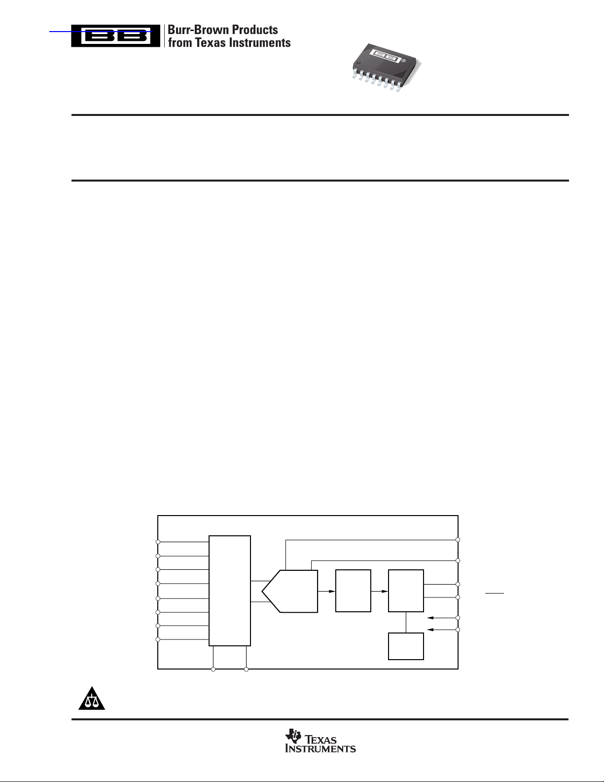
The ADS1253 is a four-channel converter and is offered in
an SSOP-16 package.
ADS1253
CH1+
CH1–
CH2+
CH2–
CH3+
CH3–
CH4+
CH4–
Please be aware that an important notice concerning availability, standard warranty, and use in critical applications of
Texas Instruments semiconductor products and disclaimers thereto appears at the end of this data sheet.
PRODUCTION DATA information is current as of publication date.
Products conform to specifications per the terms of Texas Instruments
standard warranty. Production processing does not necessarily include
testing of all parameters.
Mux
CHSEL0
CHSEL1
4th-Order
∆Σ
Modulator
www.ti.com
Digital
Filter
V
REF
CLK
Serial
Interface
Control
Copyright © 2001, Texas Instruments Incorporated
SCLK
DOUT/DRDY
+V
DD
GND
Page 2
ABSOLUTE MAXIMUM RATINGS
Analog Input: Current (Momentary) .............................................. ±100mA
(Continuous) ............................................... ±10mA
to GND ............................................................................ –0.3V to 6V
V
DD
V
Voltage to GND ............................................... –0.3V to VDD + 0.3V
REF
Digital Input Voltage to GND ................................... –0.3V to V
Digital Output Voltage to GND ................................. –0.3V to V
Lead Temperature (soldering, 10s) .............................................. +300 °C
Power Dissipation (any package) ................................................. 500mW
Voltage ................................... GND – 0.3V to V
+ 0.3V
DD
+ 0.3V
DD
+ 0.3V
DD
This integrated circuit can be damaged by ESD. Texas Instruments recommends that all integrated circuits be handled with
appropriate precautions. Failure to observe proper handling
and installation procedures can cause damage.
ESD damage can range from subtle performance degradation
ELECTROSTATIC
DISCHARGE SENSITIVITY
to complete device failure. Precision integrated circuits may
be more susceptible to damage because very small parametric
changes could cause the device not to meet its published
specifications.
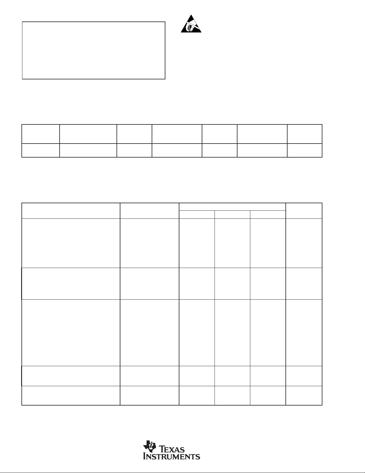
PACKAGE/ORDERING INFORMATION
PACKAGE SPECIFIED
PRODUCT PACKAGE NUMBER RANGE MARKING NUMBER
DRAWING TEMPERATURE PACKAGE ORDERING TRANSPORT
ADS1253E SSOP-16 322 –40°C to +85°C ADS1253E ADS1253E Rails
(1)
MEDIA
"""""ADS1253E/2K5 Tape and Reel
NOTE: (1) Models with a slash (/) are available only in Tape and Reel in the quantities indicated (e.g., /2K5 indicates 2500 devices per reel). Ordering 2500 pieces
of “ADS1253E/2K5” will get a single 2500-piece Tape and Reel.
ELECTRICAL CHARACTERISTICS
All specifications at T
PARAMETER CONDITIONS MIN TYP MAX UNITS
ANALOG INPUT
Input Voltage Range GND ±V
Input Impedance CLK = 3,840Hz 260 MΩ
Input Capacitance 6pF
Input Leakage At +25°C550pA
DYNAMIC CHARACTERISTICS
Data Rate 20.8 kHz
Bandwidth –3dB 4.24 kHz
Serial Clock (SCLK) 16 MHz
System Clock Input (CLK) 8 MHz
ACCURACY
Integral Non-Linearity
THD 1kHz Input; 0.1dB below FS 105 dB
Noise 1.8 2.7 ppm of FSR, rms
Resolution 24 Bits
No Missing Codes 24 Bits
Common-Mode Rejection 60Hz, AC 90 102 dB
Gain Error 0.1 1 % of FSR
Offset Error ±20 ±100 ppm of FSR
Gain Sensitivity to V
Power-Supply Rejection Ratio 70 88 dB
PERFORMANCE OVER TEMPERATURE
Offset Drift 0.07 ppm/°C
Gain Drift 0.4 ppm/°C
VOLTAGE REFERENCE
V
REF
Load Current 32 µA
NOTE: (1) Applies to full-differential signals.
MIN
REF
to T
, VDD = +5V, CLK = 8MHz, and V
MAX
(1)
= 4.096, unless otherwise specified.
REF
ADS1253E
REF
CLK = 1MHz 1 MΩ
CLK = 8MHz 125 kΩ
At T
MIN
to T
MAX
±0.0002 ±0.0015 % of FSR
1:1
0.5 4.096 V
1nA
DD
V
V
2
ADS1253
SBAS199
Page 3
ELECTRICAL CHARACTERISTICS (Cont.)
All specifications at T
PARAMETER CONDITIONS MIN TYP MAX UNITS
DIGITAL INPUT/OUTPUT
Logic Family CMOS
Logic Level: V
V
V
V
Input (SCLK, CLK, CHSEL0, CHSEL1) Hysteresis 0.6 V
Data Format
POWER-SUPPLY REQUIREMENTS
Operation +4.75 +5 +5.25 VDC
Quiescent Current 1.5 2 mA
Operating Power 7.5 10 mW
Power-Down Current 0.4 1 µA
TEMPERATURE RANGE
Operating –40 +85 °C
Storage –60 +100 °C
to T
MIN
IH
IL
OH
OL
, VDD = +5V, CLK = 8MHz, and V
MAX
= 4.096, unless otherwise specified.
REF
ADS1253E
+4.0 +VDD + 0.3 V
IOH = –500µA +4.5 V
IOL = 500µA0.4V
–0.3 +0.8 V
Offset Binary Two’s Complement
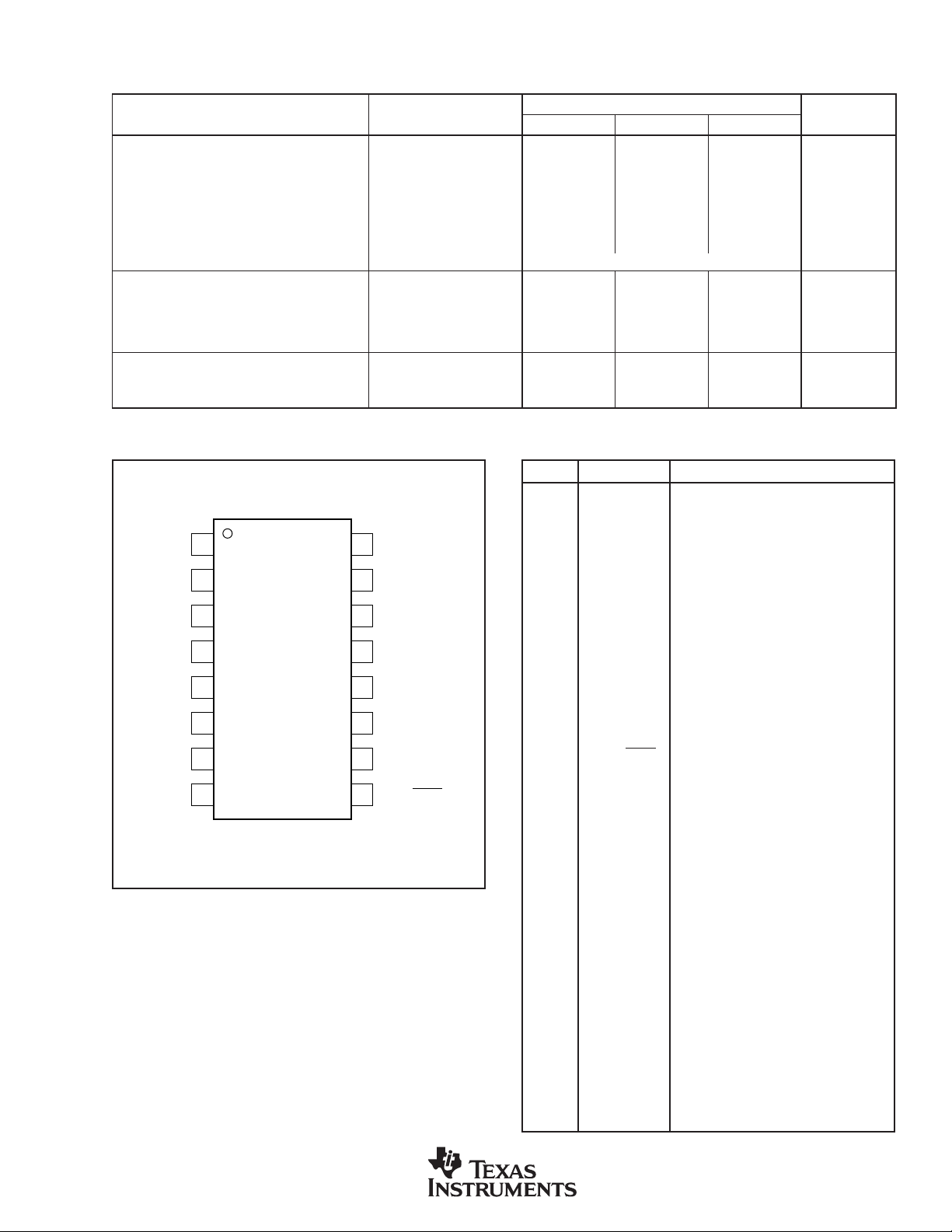
PIN CONFIGURATION
Top View SSOP-16
CH1+
CH1–
CH2+
CH2–
CH3+
CH3–
+V
CLK
1
2
3
4
5
6
7
DD
8
ADS1253E
CH4+
16
15
CH4–
V
14
13
GND
CHSEL0
12
11
CHSEL1
SCLK
10
9
DOUT/DRDY
REF
PIN DESCRIPTIONS
PIN NAME PIN DESCRIPTION
1 CH1+ Analog Input: Positive Input of the Differen-
2 CH1– Analog Input: Negative Input of the Differ-
3 CH2+ Analog Input: Positive Input of the Differen-
4 CH2– Analog Input: Negative Input of the Differ-
5 CH3+ Analog Input: Positive Input of the Differen-
6 CH3– Analog Input: Negative Input of the Differ-
7+V
8 CLK Digital Input: Device System Clock. The
9 DOUT/DRDY Digital Output: Serial Data Output/Data
10 SCLK Digital Input: Serial Clock. The serial clock
11 CHSEL1 Digital Input: Used to select analog input
12 CHSEL0 Digital Input: Used to select analog input
13 GND Input: Ground.
14 V
15 CH4– Analog Input: Negative Input of the Differ-
16 CH4+ Analog Input: Positive Input of the Differen-
DD
REF
tial Analog Input.
ential Analog Input.
tial Analog Input.
ential Analog Input.
tial Analog Input.
ential Analog Input.
Input: Power Supply Voltage, +5V.
system clock is in the form of a CMOScompatible clock. This is a Schmitt-Trigger
input.
Ready. This output indicates that a new
output word is available from the ADS1253
data output register. The serial data is
clocked out of the serial data output shift
register using SCLK.
is in the form of a CMOS-compatible clock.
The serial clock operates independently
from the system clock, therefore, it is possible to run SCLK at a higher frequency
than CLK. The normal state of SCLK is
LOW. Holding SCLK HIGH will either initiate a modulator reset for synchronizing
multiple converters or enter power-down
mode. This is a Schmitt-Trigger input.
channel. This is a Schmitt-Trigger input.
channel. This is a Schmitt-Trigger input.
Analog Input: Reference Voltage Input.
ential Analog Input.
tial Analog Input.
ADS1253
SBAS199
3
Page 4
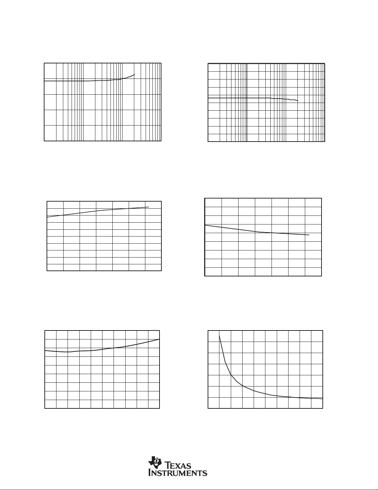
TYPICAL CHARACTERISTICS
At TA = +25°C, VDD = +5V, CLK = 8MHz, and V
= 4.096, unless otherwise specified.
REF
2.0
RMS NOISE vs DATA OUTPUT RATE
1.8
1.6
1.4
RMS Noise (ppm of FS)
1.2
1.0
100 1k 10k 100k
Data Output Rate (Hz)
2.0
1.8
1.6
1.4
1.2
1.0
0.8
0.6
RMS Noise (ppm of FS)
0.4
0.2
0.0
–40 –20 0 20 40 60 80 100
RMS NOISE vs TEMPERATURE
Temperature (°C)
20.0
EFFECTIVE RESOLUTION vs DATA OUTPUT RATE
19.8
19.6
19.4
19.2
19.0
18.8
18.6
18.4
Effective Resolution (Bits)
18.2
18.0
1k100 10k 100k
Data Output Rate (Hz)
EFFECTIVE RESOLUTION vs TEMPERATURE
20.0
19.8
19.6
19.4
19.2
19.0
18.8
18.6
18.4
Effective Resolution (Bits)
18.2
18.0
–40 –20 0 20 40 60 80 100
Temperature (°C)
18
RMS NOISE vs V
16
14
12
10
8
6
RMS Noise (µV)
4
2
0
0.50.0 1.0 1.5 2.0 2.5 3.0 3.5 4.0 4.5 5.0
V
REF
4
VOLTAGE
REF
Voltage (V)
14
RMS NOISE vs V
VOLTAGE
REF
12
10
8
6
4
RMS Noise (ppm of FS)
2
0
0.0 1.0 1.50.5 2.0 2.5 3.0 3.5 4.0 4.5 5.0
V
(V)
REF
ADS1253
SBAS199
Page 5
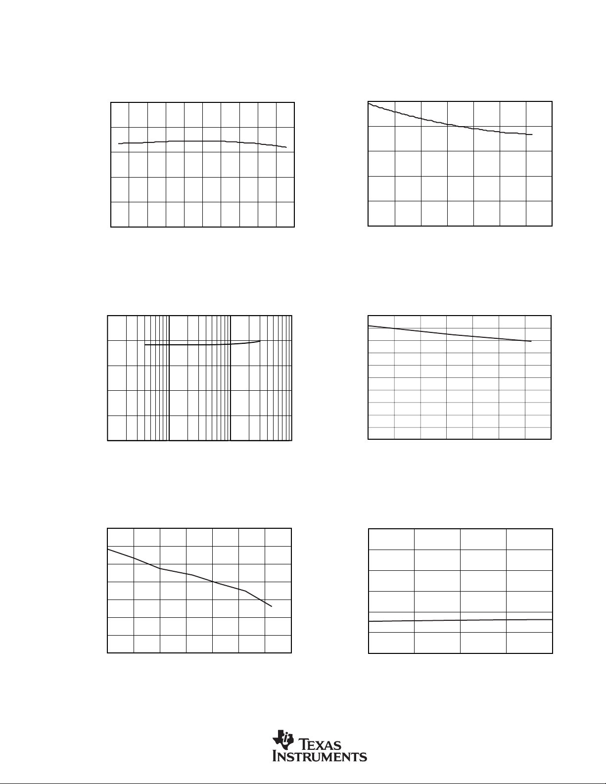
TYPICAL CHARACTERISTICS (Cont.)
OFFSET vs TEMPERATURE
20
18
16
14
12
10
8
6
4
2
0
DC Offset (ppm of FS)
–40 –20 0 20 40 60 80 100
Temperature (°C)
At TA = +25°C, VDD = +5V, CLK = 8MHz, and V
= 4.096, unless otherwise specified.
REF
2.0
1.8
1.6
1.4
RMS Noise (ppm of FS)
1.2
1.0
5
4
3
RMS NOISE vs INPUT VOLTAGE (V
–5 –4 –3 –2 –1 0 1 2 3 4 5
Input Voltage (V)
INTEGRAL NON-LINEARITY vs DATA OUTPUT RATE
REF
= 5.0V)
INTEGRAL NON-LINEARITY vs TEMPERATURE
5
4
3
2
INL (ppm of FS)
1
0
–40 –20 0 20 40 60 80 100
Temperature (°C)
2
INL (ppm of FS)
1
0
100 1k 10k 100k
Data Output Rate (Hz)
570
560
550
540
530
520
Gain Error (ppm of FS)
510
500
–40 –20 0 20 40 60 80 100
ADS1253
SBAS199
GAIN ERROR vs TEMPERATURE
Temperature (°C)
0
–20
–40
–60
PSRR (dB)
–80
–100
–120
02468
PSRR vs CLK FREQUENCY
Clock Frequency (MHz)
5
Page 6
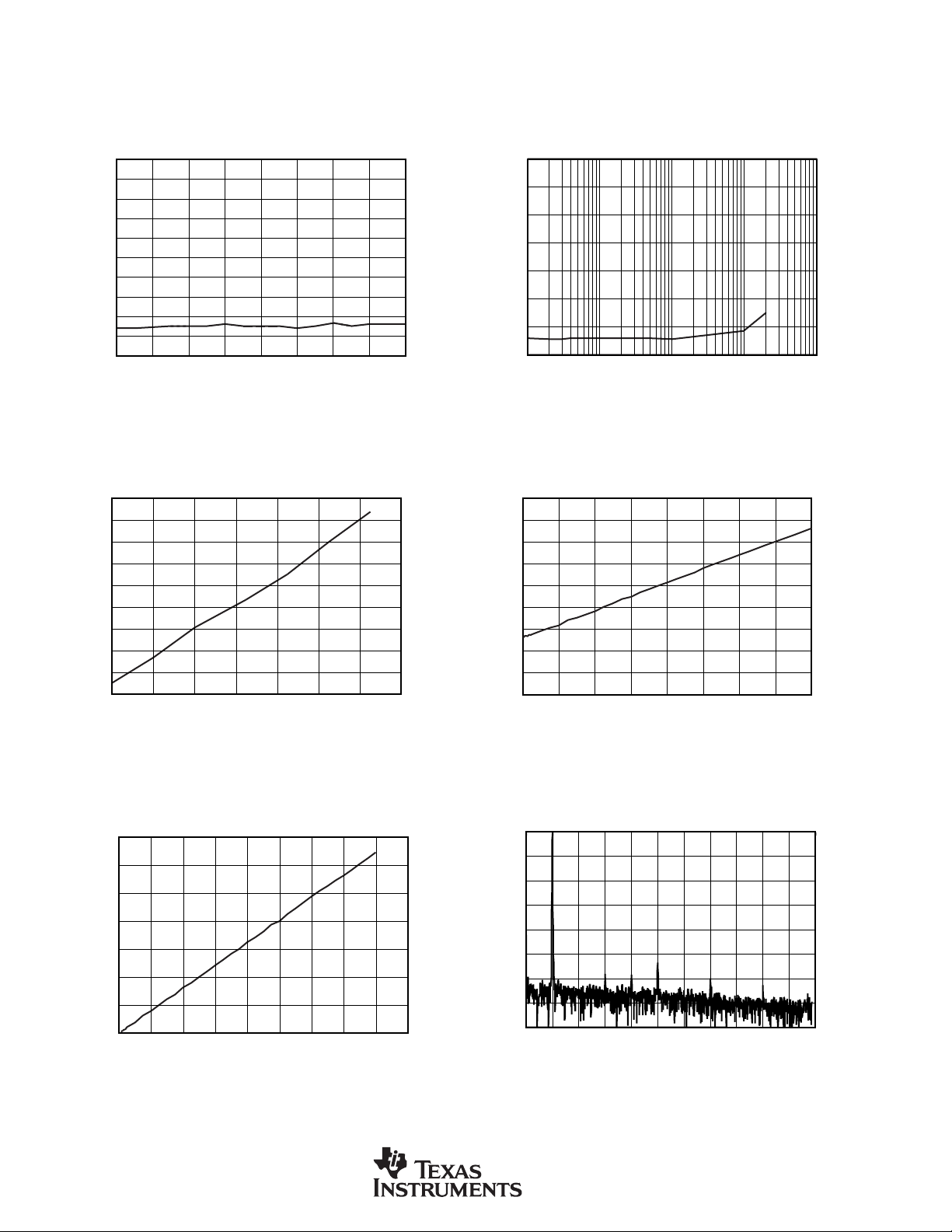
TYPICAL CHARACTERISTICS (Cont.)
At TA = +25°C, VDD = +5V, CLK = 8MHz, and V
= 4.096, unless otherwise specified.
REF
–60
–65
–70
–75
–80
–85
–90
–95
CMR at 60Hz (dB)
–100
–105
–110
012345678
1.64
1.62
1.60
1.58
1.56
1.54
Current (mA)
1.52
1.50
1.48
1.46
–40 –20 0 20 40 60 80 100
CMR AT 60Hz vs CLK FREQUENCY
Clock Frequency (MHz)
CURRENT vs TEMPERATURE
Temperature (°C)
a0873473
nn
–70
–75
–80
–85
–90
CMR (dB)
–95
–100
–105
10 100 1k 10k 100k
9
8
7
6
5
4
3
2
Power Dissipation (mW)
1
0
POWER DISSIPATION vs CLK FREQUENCY
012345 768
CMR vs FREQUENCY
Common-Mode Signal Frequency (Hz)
Clock Frequency (MHz)
V
CURRENT vs CLK FREQUENCY
35
30
25
20
15
Current (µA)
REF
V
10
5
0
0123456789
REF
Clock Frequency (MHz)
0
–20
–40
–60
–80
–100
–120
Relative Magnitude (dB)
–140
–160
01234567891011
(1kHz input at 0.1dB less than full-scale)
6
TYPICAL FFT
Input Signal Frequency (kHz)
ADS1253
SBAS199
Page 7

THEORY OF OPERATION
10kΩ
20kΩ
R
1
OPA4350
OPA4350
OPA4350
+IN
–IN
V
REF
ADS1253
R
2
Bipolar
Input
REF
2.5V
The ADS1253 is a precision, high-dynamic range, 24-bit,
delta-sigma, A/D converter capable of achieving very
high-resolution digital results at high data rates.
The analog-input signal is sampled at a rate determined by the
frequency of the system clock (CLK). The sampled analog
input is modulated by the delta-sigma A/D modulator, which
is followed by a digital filter. A sinc5 digital low-pass filter
processes the output of the delta-sigma modulator and writes
the result into the data-output register. The DOUT/DRDY pin
is pulled LOW, indicating that new data is available to be read
by the external microcontroller/microprocessor. As shown in
the block diagram, the main functional blocks of the ADS1253
are the fourth-order delta-sigma modulator, a digital filter,
control logic, input multiplexer, and a serial interface. Each of
these functional blocks is described below.
ANALOG INPUT
The ADS1253 contains a fully differential analog input. In
order to provide low system noise, common-mode rejection
of 98dB and excellent power-supply rejection, the design
topology is based on a fully differential switched-capacitor
architecture. The bipolar input voltage range is from –4.096
to +4.096V, when the reference input voltage equals +4.096V.
The bipolar range is with respect to –VIN, and not with
respect to GND.
Figure 1 shows the basic input structure of the ADS1253.
The impedance is directly related to the sampling frequency
of the input capacitor which is set by the CLK rate. Higher
CLK rates result in lower impedance, and lower CLK rates
result in higher impedance.
R
SW
(1300Ω typical)
A
IN
Modulator Frequency
= f
MOD
FIGURE 1. Analog-Input Structure.
V
CM
Internal
Circuitry
C
INT
(6pF typical)
system clock frequency of 8MHz, the data-output rate is
20.8kHz with a –3dB frequency of 4.24kHz. The –3dB
frequency scales with the system clock frequency.
To guarantee the best linearity of the ADS1253, a fully
differential signal is recommended, and the capacitance to
ground must be equal on both sides.
INPUT MULTIPLEXER
The CHS1 and CHS0 pins are used to select the analog input
channel as shown in Table I. The recommended method for
changing channels is to change the channel after the conversion from the previous channel has been completed and read.
When a channel is changed, internal logic senses the change
on the falling edge of CLK and resets the conversion
process. The conversion data from the new channel is valid
on the first DRDY after the channel change.
When multiplexing inputs it is possible to achieve sample rates
close to 4kHz. This is due to the fact that it requires five internal
conversion cycles for the data to fully settle, the data also must
be read before the channel is changed. The DRDY signal
indicates a valid result after the five cycles have occurred
CHSEL1 CHSEL0 CHANNEL
0 0 CH1
0 1 CH2
1 0 CH3
1 1 CH4
TABLE I. Channel Selection.
BIPOLAR INPUT
Each of the differential inputs of the ADS1253 must stay
between AGND – 0.3V and V
+ 0.3V. With a reference
DD
voltage at less than half of VDD, one input can be tied to the
reference voltage, and the other input can range from 0 to
2 • V
. By using a three op amp circuit featuring a single
REF
amplifier and four external resistors, the ADS1253 can be
configured to accept bipolar inputs referenced to ground.
The conventional ±2.5V, ±5V, and ±10V input ranges can
be interfaced to the ADS1253 using the resistor values
shown in Figure 2.
The input impedance of the analog input changes with
ADS1253 system clock frequency (CLK). The relationship is:
AIN Impedance (Ω) = (8MHz/CLK) • 125,000
With regard to the analog-input signal, the overall analog
performance of the device is affected by three items: first, the
input impedance can affect accuracy. If the source impedance
of the input signal is significant, or if there is passive filtering
prior to the ADS1253, a significant portion of the signal can
be lost across this external impedance. The magnitude of the
effect is dependent on the desired system performance.
Second, the current into or out of the analog inputs must be
limited. Under no conditions should the current into or out
of the analog inputs exceed 10mA.
Third, to prevent aliasing of the input signal, the analog-input
signal must be band limited. The bandwidth of the A/D
converter is a function of the system clock frequency. With a
ADS1253
SBAS199
BIPOLAR INPUT R
±10V 2.5kΩ 5kΩ
±5V 5kΩ 10kΩ
±2.5V 10kΩ 20kΩ
R
1
2
FIGURE 2. Level Shift Circuit for Bipolar Input Ranges.
7
Page 8

DELTA-SIGMA MODULATOR
The ADS1253 operates from a nominal system clock frequency of 8MHz. The modulator frequency is fixed in
relation to the system clock frequency. The system clock
frequency is divided by 6 to derive the modulator frequency.
Therefore, with a system clock frequency of 8MHz, the
modulator frequency is 1.333MHz. Furthermore, the
oversampling ratio of the modulator is fixed in relation to the
modulator frequency. The oversampling ratio of the modulator is 64, and with the modulator frequency running at
1.333MHz, the data rate is 20.8kHz. Using a slower system
clock frequency will result in a lower data output rate, as
shown in Table II.
CLK (MHz) DATA OUTPUT RATE (Hz)
(1)
8
(1)
7.372800
(1)
6.144000
(1)
6.000000
(1)
4.915200
(1)
3.686400
(1)
3.072000
(1)
2.457600
(1)
1.843200
0.921600 2,400
0.460800 1,200
0.384000 1,000
0.192000 500
0.038400 100
0.023040 60
0.019200 50
0.011520 30
0.009600 25
0.007680 20
0.006400 16.67
0.005760 15
0.004800 12.50
0.003840 10
NOTE: (1) Standard Clock Oscillator.
20,833
19,200
16,000
15,625
12,800
9,600
8,000
6,400
4,800
TABLE II. CLK Rate versus Data Output Rate.
REFERENCE INPUT
Reference input takes an average current of 32µA with a
8MHz system clock. This current will be proportional to the
system clock. A buffered reference is recommended for
ADS1253. The recommended reference circuit is shown in
Figure 3.
Reference voltages higher than 4.096V will increase the
full-scale range, while the absolute internal circuit noise of
the converter remains the same. This will decrease the noise
in terms of ppm of full scale, which increases the effective
resolution (see the Typical Performance Curve “RMS Noise
vs V
Voltage”).
REF
DIGITAL FILTER
The digital filter of the ADS1253, referred to as a sinc5 filter,
computes the digital result based on the most recent outputs
from the delta-sigma modulator. At the most basic level, the
digital filter can be thought of as simply averaging the
modulator results in a weighted form and presenting this
average as the digital output. The digital output rate, or data
rate, scales directly with the system CLK frequency. This
allows the data output rate to be changed over a very wide
range (five orders of magnitude) by changing the system
CLK frequency. However, it is important to note that the
–3dB point of the filter is 0.2035 times the data output rate,
so the data output rate should allow for sufficient margin to
prevent attenuation of the signal of interest.
Since the conversion result is essentially an average, the
data-output rate determines the location of the resulting
notches in the digital filter (see Figure 4). Note that the first
notch is located at the data-output rate frequency, and
subsequent notches are located at integer multiples of the
data-output rate to allow for rejection of not only the
fundamental frequency, but also harmonic frequencies. In
this manner, the data-output rate can be used to set specific
notch frequencies in the digital filter response.
For example, if the rejection of power-line frequencies is
desired, then the data-output rate can simply be set to the
power-line frequency. For 50Hz rejection, the system CLK
2
3
+5V
0.10µF
7
OPA350
4
6
+
10µF
0.1µF
To V
REF
Pin 14 of
the ADS1253
+5V
1
4.99kΩ
10kΩ
LM404-4.1
+
10µF
0.10µF
FIGURE 3. Recommended External Voltage Reference Circuit for Best Low-Noise Operation with the ADS1253.
8
ADS1253
SBAS199
Page 9

DIGITAL FILTER RESPONSE
0
–20
–40
–60
–80
–100
–120
–140
–160
–180
–200
10 20 30 40 50 60 70 80 90 1000
Frequency (Hz)
Gain (dB)
0
DIGITAL FILTER RESPONSE
0
–20
–40
–60
–80
–100
–120
–140
–160
–180
–200
50 100 150 200 250 3000
Frequency (Hz)
Gain (dB)
–20
–40
–60
–80
–100
–120
Gain (dB)
–140
–160
–180
–200
NORMALIZED DIGITAL FILTER RESPONSE
123456789100
Frequency (Hz)
FIGURE 4. Normalized Digital Filter Response.
0
–20
–40
–60
–80
–100
–120
Gain (dB)
–140
–160
–180
–200
DIGITAL FILTER RESPONSE
50 100 150 200 250 3000
Frequency (Hz)
FIGURE 5. Digital Filter Response (50Hz).
FIGURE 6. Digital Filter Response (60Hz). FIGURE 7. Digital Filter Response (10Hz).
0
–20
–40
–60
–80
–100
–120
Gain (dB)
–140
–160
–180
–200
46 47 48 49 50 51 52 53 54 5545
DIGITAL FILTER RESPONSE
Frequency (Hz)
FIGURE 8. Expanded Digital Filter Response (50Hz with a
50Hz Data Output Rate).
0
–20
–40
–60
–80
–100
–120
Gain (dB)
–140
–160
–180
–200
46 47 48 49 50 51 52 53 54 5545
FIGURE 9. Expanded Digital Filter Response (50Hz with a
10Hz Data Output Rate).
DIGITAL FILTER RESPONSE
Frequency (Hz)
ADS1253
SBAS199
9
Page 10

Gain (dB)
–20
–40
–60
–80
–100
–120
–140
–160
–180
–200
0
DIGITAL FILTER RESPONSE
56 57 58 59 60 61 62 63 64 6555
Frequency (Hz)
Gain (dB)
0
–20
–40
–60
–80
–100
–120
–140
–160
–180
–200
56 57 58 59 60 61 62 63 64 6555
DIGITAL FILTER RESPONSE
Frequency (Hz)
FIGURE 10. Expanded Digital Filter Response (60Hz with
a 60Hz Data Output Rate).
frequency should be 19.200kHz, this will set the data-output
rate to 50Hz (see Table I and Figure 5). For 60Hz rejection,
the system CLK frequency should be 23.040kHz, this will
set the data-output rate to 60Hz (see Table I and Figure 6).
If both 50Hz and 60Hz rejection is required, then the system
CLK should be 3.840kHz; this will set the data-output rate
to 10Hz and reject both 50Hz and 60Hz (See Table I and
Figure 7).
There is an additional benefit in using a lower data-output
rate. It provides better rejection of signals in the frequency
band of interest. For example, with a 50Hz data-output rate,
a significant signal at 75Hz may alias back into the passband
at 25Hz. This is due to the fact that rejection at 75Hz may
only be 66dB in the stopband—frequencies higher than the
first-notch frequency (see Figure 5). However, setting the
data-output rate to 10Hz will provide 135dB rejection at
75Hz (see Figure 7). A similar benefit is gained at frequencies near the data-output rate (see Figures 8, 9, 10, and 11).
For example, with a 50Hz data-output rate, rejection at 55Hz
may only be 105dB (see Figure 8). However, with a 10Hz
data-output rate, rejection at 55Hz will be 122dB (see
Figure 9). If a slower data-output rate does not meet the
system requirements, then the analog front end can be
designed to provide the needed attenuation to prevent aliasing.
Additionally, the data-output rate may be increased and
additional digital filtering may be done in the processor or
controller.
FIGURE 11. Expanded Digital Filter Response (60Hz with
a 10Hz Data Output Rate).
The digital filter is described by the following transfer
function:
• •
f
MOD
f
f
64
•ππ
MOD
f
H f
( )
sin
=
•sin
64
5
or
5
64
–
z
1
–
z
H z
( )
=
64 1
1
–
• –
( )
The digital filter requires five conversions to fully settle. The
modulator has an oversampling ratio of 64, therefore, it
requires 5 • 64, or 320 modulator results, or clocks, to fully
settle. Since the modulator clock is derived from the system
clock (CLK) (modulator clock = CLK ÷ 6), the number of
system clocks required for the digital filter to fully settle is
5 • 64 • 6, or 1920 CLKs. This means that any significant
step change at the analog input requires five full conversions
to settle. However, if the step change at the analog input
occurs asynchronously to the DOUT/DRDY pulse, six conversions are required to ensure full settling.
10
ADS1253
SBAS199
Page 11

CONTROL LOGIC
The control logic is used for communications and control of
the ADS1253.
Power-Up Sequence
Prior to power-up, all digital and analog-input pins must be
LOW. At the time of power-up, these signal inputs can be
biased to a voltage other than 0V, however, they should
never exceed +VDD.
Once the ADS1253 powers up, the DOUT/DRDY line will
pulse LOW on the first conversion for which the data is valid
from the analog input signal.
DOUT/DRDY
The DOUT/DRDY output signal alternates between two
modes of operation. The first mode of operation is the Data
Ready mode (DRDY) to indicate that new data has been
loaded into the data-output register and is ready to be read.
The second mode of operation is the Data Output (DOUT)
mode and is used to serially shift data out of the Data Output
Register (DOR). See Figure 12 for the time domain partitioning of the DRDY and DOUT function.
See Figure 14 for the basic timing of DOUT/DRDY. During
the time defined by t2, t3, and t4, the DOUT/DRDY pin
functions in DRDY mode. The state of the
DOUT/DRDY pin would be HIGH prior to the internal
transfer of new data to the DOR. The result of the A/D
conversion would be written to the DOR from MSB to LSB
in the time defined by t1 (see Figures 12 and 14). The
DOUT/DRDY line would then pulse LOW for the time
defined by t2, and then pulse HIGH for the time defined by
t3 to indicate that new data was available to be read. At this
point, the function of the DOUT/DRDY pin would change
to DOUT mode. Data would be shifted out on the pin after
t7. The device communicating with the ADS1253 can provide SCLKs to the ADS1253 after the time defined by t6.
The normal mode of reading data from the ADS1253 would
be for the device reading the ADS1253 to latch the data on
the rising edge of SCLK (since data is shifted out of the
ADS1253 on the falling edge of SCLK). In order to retrieve
valid data, the entire DOR must be read before the
DOUT/DRDY pin reverts back to DRDY mode.
If SCLKs were not provided to the ADS1253 during the
DOUT mode, the MSB of the DOR would be present on the
DOUT/DRDY line until the time defined by t4. If an incomplete read of the ADS1253 took place while in DOUT mode
(i.e., less than 24 SCLKs were provided), the state of the last
bit read would be present on the DOUT/DRDY line until the
time defined by t4. If more than 24 SCLKs were provided
during DOUT mode, the DOUT/DRDY line would stay
LOW until the time defined by t4.
The internal data pointer for shifting data out on
DOUT/DRDY is reset on the falling edge of the time defined
by t1 and t4. This ensures that the first bit of data shifted out
of the ADS1253 after DRDY mode is always the MSB of
new data.
SYNCHRONIZING MULTIPLE CONVERTERS
The normal state of SCLK is LOW, however, by holding
SCLK HIGH, multiple ADS1253s can be synchronized. This
is accomplished by holding SCLK HIGH for at least four, but
less than twenty, consecutive DOUT/DRDY cycles (see Figure 15). After the ADS1253 circuitry detects that SCLK has
been held HIGH for four consecutive DOUT/DRDY cycles,
the DOUT/DRDY pin will pulse LOW for 3 CLK cycles and
then be held HIGH, and the modulator will be held in a reset
state. The modulator will be released from reset and synchronization will occur on the falling edge of SCLK. With
multiple converters the falling edge transition of SCLK must
occur simultaneously on all devices. It is important to note
that prior to synchronization, the DOUT/DRDY pulse of
multiple ADS1253s in the system could have a difference in
timing up to one DRDY period. Therefore to ensure synchronization, the SCLK should be held HIGH for at least five
DRDY cycles. The first DOUT/DRDY pulse after the falling
edge of SCLK will occur at t14. The first DOUT/DRDY pulse
indicates valid data.
POWER-DOWN MODE
The normal state of SCLK is LOW, however, by holding
SCLK HIGH, the ADS1253 will enter power-down mode.
This is accomplished by holding SCLK HIGH for at least
twenty consecutive DOUT/DRDY periods (see Figure 15).
After the ADS1253 circuitry detects that SCLK has been
held HIGH for four consecutive DOUT/DRDY cycles, the
DOUT/DRDY pin will pulse LOW for 3 CLK cycles and
then be held HIGH, and the modulator will be held in a
reset state. If SCLK is held HIGH for an additional sixteen
DOUT/DRDY periods, the ADS1253 will enter
power-down mode. The part will be released from powerdown mode on the falling edge of SCLK. It is important to
note that the DOUT/DRDY pin will be held HIGH after four
DOUT/DRDY cycles, but power-down mode will not be
entered for an additional sixteen DOUT/DRDY periods. The
first DOUT/DRDY pulse after the falling edge of SCLK will
occur at t
and will indicate valid data. Subsequent
16
DOUT/DRDY pulses will occur normally.
DOUT/DRDY
DATA
FIGURE 12. DOUT/DRDY Partitioning.
ADS1253
SBAS199
DRDY Mode
t
4
t
1
t2t
DOUT ModeDOUT Mode
3
DATA DATA
DRDY Mode
11
Page 12
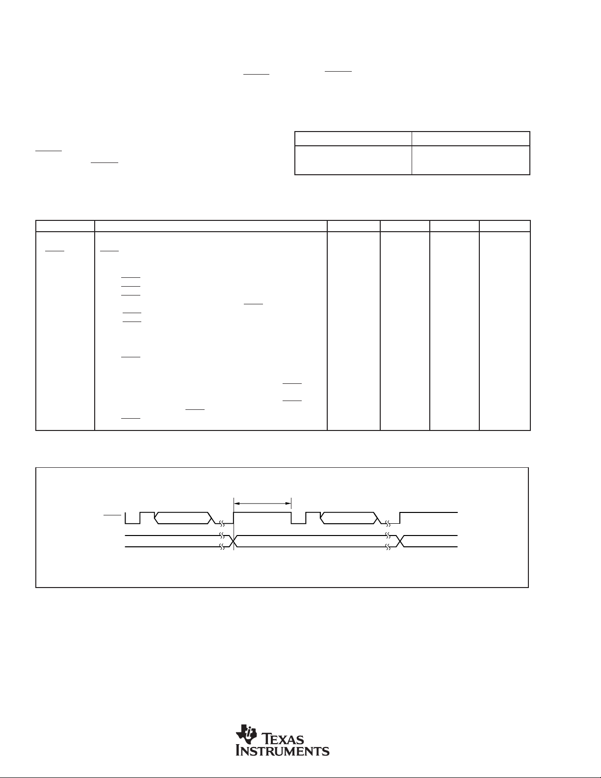
SERIAL INTERFACE
The ADS1253 includes a simple serial interface which can
be connected to microcontrollers and digital signal processors in a variety of ways. Communications with the ADS1253
can commence on the first detection of the DOUT/DRDY
pulse after power up.
It is important to note that the data from the ADS1253 is a
24-bit result transmitted MSB-first in Offset Two’s Comple-
ISOLATION
The serial interface of the ADS1253 provides for simple
isolation methods. The CLK signal can be local to the
ADS1253, which then only requires two signals (SCLK, and
DOUT/DRDY) to be used for isolated data acquisition. The
channel select signals (CHS0, CHS1) will also need to be
isolated unless a counter is used to auto multiplex the
channels.
ment format, as shown in Table IV.
The data must be clocked out before the ADS1253 enters
DRDY mode to ensure reception of valid data, as described
in the DOUT/DRDY section of this data sheet.
DIFFERENTIAL VOLTAGE INPUT DIGITAL OUTPUT (HEX)
+Full Scale 7FFFFFH
Zero 000000H
–Full Scale 800000H
TABLE IV. ADS1253 Data Format (Offset Two's Comple-
ment).
SYMBOL DESCRIPTION MIN TYP MAX UNITS
t
OSC
t
DRDY
DRDY Mode DRDY Mode 36 • t
DOUT Mode DOUT Mode 348 • t
t
1
t
2
t
3
t
4
t
5
t
6
t
7
t
8
t
9
t
10
t
11
t
12
t
13
t
14
t
15
t
16
t
17
t
18
CLK Period 125 ns
Conversion Cycle 384 • t
DOR Write Time 6 • t
DOUT/DRDY LOW Time 6 • t
DOUT/DRDY HIGH Time (Prior to Data Out) 6 • t
DOUT/DRDY HIGH Time (Prior to Data Ready) 24 • t
Rising Edge of CLK to Falling Edge of DOUT/DRDY 30 ns
End of DRDY Mode to Rising Edge of First SCLK 30 ns
End of DRDY Mode to Data Valid (Propagation Delay) 30 ns
Falling Edge of SCLK to Data Valid (Hold Time) 5 ns
Falling Edge of SCLK to Next Data Out Valid (Propagation Delay) 30 ns
SCLK Setup Time for Synchronization or Power Down 30 ns
DOUT/DRDY Pulse for Synchronization or Power Down 3 • t
Rising Edge of SCLK Until Start of Synchronization 1537 • CLK 7679 • CLK ns
Synchronization Time 0.5 • CLK 6143.5 • CLK ns
Falling Edge of CLK (After SCLK Goes Low) Until Start of DRDY Mode 2042.5 • t
Rising Edge of SCLK Until Start of Power Down 7681 • CLK ns
Falling Edge of CLK (After SCLK Goes Low) Until Start of DRDY Mode 2318.5 • t
Falling Edge of Last DOUT/DRDY to Start of Power Down 6144.5 • t
DOUT/DRDY High Time After Mux Change. 2043.5 • tosc
OSC
OSC
OSC
OSC
OSC
OSC
OSC
OSC
OSC
OSC
OSC
ns
ns
ns
ns
ns
ns
ns
ns
ns
ns
ns
TABLE III. Digital Timing.
DOUT/DRDY
CHS0, CHS1
FIGURE 13. Multiplexer Operation.
t
18
DATA DATA
MUX CHANGE
12
ADS1253
SBAS199
Page 13
CLK
DOUT/DRDY
SCLK
t
5
t
1
t
2
t
3
t
4
t
7
t
6
t
8
t
9
DRDY Mode
DOUT Mode
t
DRDY
MSB LSB
CLK
DOUT/DRDY
SCLK
t
3
t
4
t
12
t
2
t
11
t
13
t
14
t
DRDY
t
10
t
DRDY
4 t
DRDY
DATA
DATA
DATA
Synchronization Mode Starts Here
Synchronization Begins Here
DOUT
Mode
t
3
t
4
t
2
DOUT
Mode
CLK
DOUT/DRDY
SCLK
t
3
t
4
t
15
t
2
t
11
t
17
t
16
t
DRDY
t
10
t
DRDY
4 t
DRDY
DATA
DATA
DATA
Power Down Occurs Here
DOUT
Mode
t
3
t
4
t
2
DOUT
Mode
t
11
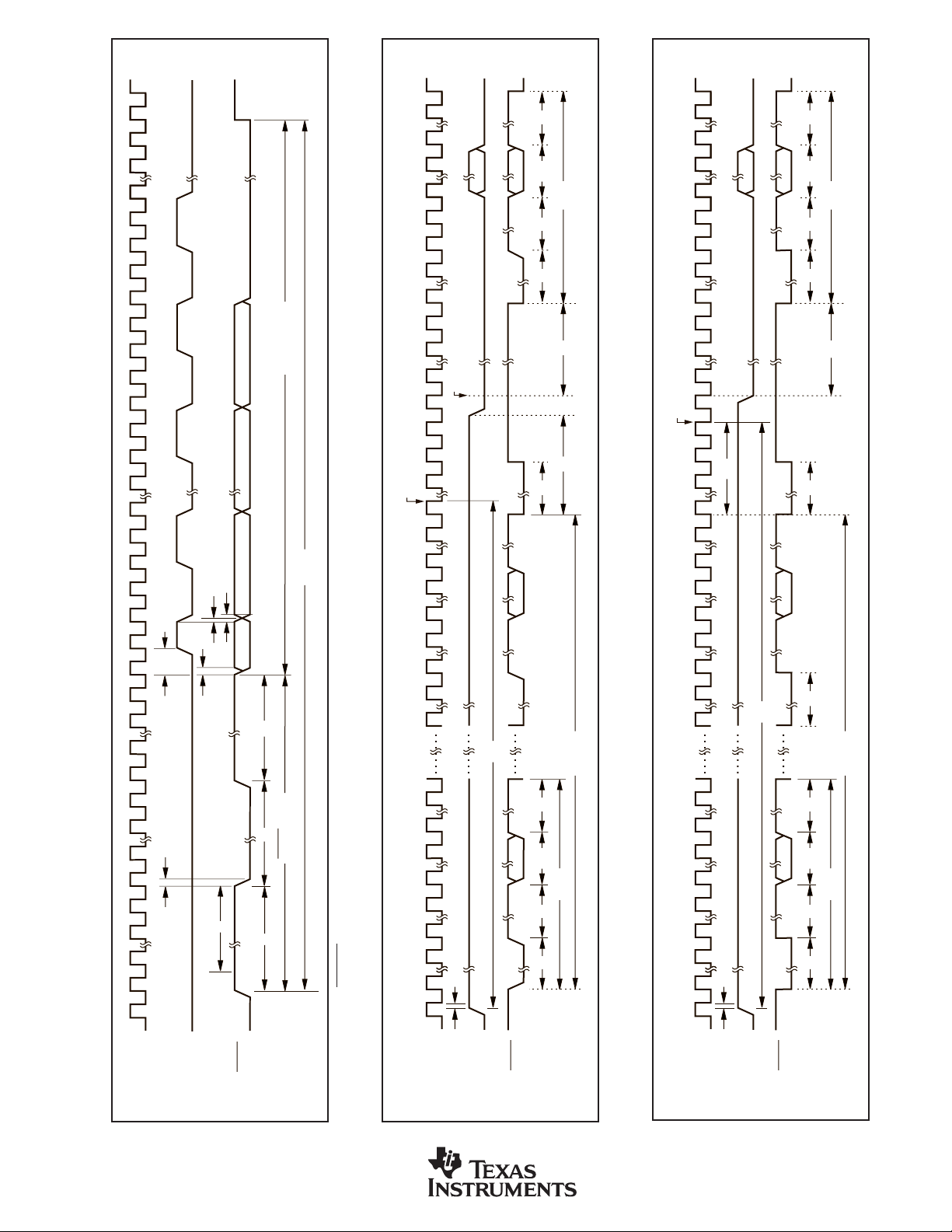
FIGURE 14. DOUT/DRDY Timing.
FIGURE 15. Synchronization Mode.
FIGURE 16. Power-Down Mode.
ADS1253
SBAS199
13
Page 14

LAYOUT
POWER SUPPLY
The power supply should be well regulated and low noise.
For designs requiring very high resolution from the ADS1253,
power-supply rejection will be a concern. Avoid running
digital lines under the device as they may couple noise onto
the die. High-frequency noise can capacitively couple into
the analog portion of the device and will alias back into the
passband of the digital filter, affecting the conversion result.
This clock noise will cause an offset error.
GROUNDING
The analog and digital sections of the system design should
be carefully and cleanly partitioned. Each section should
have its own ground plane with no overlap between them.
GND should be connected to the analog ground plane, as
well as all other analog grounds. Do not join the analog and
digital ground planes on the board, but instead connect the
two with a moderate signal trace. For multiple converters,
connect the two ground planes at one location as central to
all of the converters as possible. In some cases, experimentation may be required to find the best point to connect the
two planes together. The printed circuit board can be designed to provide different analog/digital ground connections via short jumpers. The initial prototype can be used to
establish which connection works best.
could include:
• Multiple ADS1253s
• Extensive Analog Signal Processing
• One or More Microcontrollers, Digital Signal Processors,
or Microprocessors
• Many Different Clock Sources
• Interconnections to Various Other Systems
High resolution will be very difficult to achieve for this
design. The approach would be to break the system into as
many different parts as possible. For example, each ADS1253
may have its own “analog” processing front end.
DEFINITION OF TERMS
An attempt has been made to be consistent with the terminology used in this data sheet. In that regard, the definition
of each term is given as follows:
Analog-Input Differential Voltage—for an analog signal
that is fully differential, the voltage range can be compared
to that of an instrumentation amplifier. For example, if both
analog inputs of the ADS1253 are at 2.048V, the differential voltage is 0V. If one analog input is at 0V and the other
analog input is at 4.096V, then the differential voltage
magnitude is 4.096V. This is the case regardless of which
input is at 0V and which is at 4.096V. The digital-output
result, however, is quite different. The analog-input differential voltage is given by the following equation:
DECOUPLING
Good decoupling practices should be used for the ADS1253
and for all components in the design. All decoupling capacitors, and specifically the 0.1µF ceramic capacitors, should
be placed as close as possible to the pin being decoupled. A
1µF to 10µF capacitor, in parallel with a 0.1µF ceramic
capacitor, should be used to decouple VDD to GND.
SYSTEM CONSIDERATIONS
The recommendations for power supplies and grounding
will change depending on the requirements and specific
design of the overall system. Achieving 24 bits of noise
performance is a great deal more difficult than achieving 12
bits of noise performance. In general, a system can be
broken up into four different stages:
• Analog Processing
• Analog Portion of the ADS1253
• Digital Portion of the ADS1253
• Digital Processing
For the simplest system consisting of minimal analog signal
processing (basic filtering and Gain), a microcontroller, and
one clock source, one can achieve high resolution by powering all components by a common power supply. In addition, all components could share a common ground plane.
Thus, there would be no distinctions between “analog”
power and ground, and “digital” power and ground. The
layout should still include a power plane, a ground plane,
and careful decoupling. In a more extreme case, the design
+VIN – (–VIN)
A positive digital output is produced whenever the
analog-input differential voltage is positive, while a negative digital output is produced whenever the differential is
negative. For example, a positive full-scale output is produced when the converter is configured with a 4.096V
reference, and the analog-input differential is 4.096V. The
negative full-scale output is produced when the differential
voltage is –4.096V. In each case, the actual input voltages
must remain within the –0.3V to +VDD range.
Actual Analog-Input Voltage—the voltage at any one
analog input relative to GND.
Full-Scale Range (FSR)—as with most ADC’s, the fullscale range of the ADS1253 is defined as the “input” which
produces the positive full-scale digital output minus the
“input” which produces the negative full-scale digital output. For example, when the converter is configured with a
4.096V reference, the differential full-scale range is:
[4.096V (positive full scale) – (–4.096V) (negative full scale)] =
8.192V
Least Significant Bit (LSB) Weight—this is the theoretical amount of voltage that the differential voltage at the
analog input would have to change in order to observe a
change in the output data of one least significant bit. It is
computed as follows:
LSB
Weight
where N is the number of bits in the digital output.
Full – Scale Range
= =
N N
2 –1 2 –1
2•
V
REF
14
ADS1253
SBAS199
Page 15

Conversion Cycle—as used here, a conversion cycle refers
to the time period between DOUT/DRDY pulses.
Effective Resolution (ER)—of the ADS1253 in a particular
configuration can be expressed in two different units:
bits rms (referenced to output) and µVrms (referenced to
input). Computed directly from the converter's output data,
each is a statistical calculation based on a given number of
results. Noise occurs randomly; the rms value represents a
statistical measure which is one standard deviation. The ER
in bits can be computed as follows:
2• V
The 2 • V
20• log
ER in bits rms =
figure in each calculation represents the
REF
Vrms noise
6.02
REF
full-scale range of the ADS1253. This means that both units
are absolute expressions of resolution—the performance in
different configurations can be directly compared, regardless of the units.
f
—frequency of the modulator and the frequency the
MOD
input is sampled.
CLK
=
Frequency
6
f
—Data output rate.
DATA
f
MOD
Noise Reduction—for random noise, the ER can be improved with averaging. The result is the reduction in noise
by the factor √N, where N is the number of averages, as
shown in Table V. This can be used to achieve true 24-bit
performance at a lower data rate. To achieve 24 bits of
resolution, more than 24 bits must be accumulated. A 36-bit
accumulator is required to achieve an ER of 24 bits. The
following uses V
= 4.096V, with the ADS1253 output-
REF
ting data at 20kHz, a 4096 point average will take 204.8ms.
The benefits of averaging will be degraded if the input signal
drifts during that 200ms.
N NOISE ER ER
(Number REDUCTION IN IN
of Averages) FACTOR Vrms BITS rms
1 1 14.6µV 19.1
2 1.414 10.3µV 19.6
4 2 7.3µV 20.1
82.825.16µV 20.6
16 4 3.65µV 21.1
32 5.66 2.58µV 21.6
64 8 1.83µV 22.1
128 11.3 1.29µV 22.6
256 16 0.91µV 23.1
512 22.6 0.65µV 23.6
1024 32 0.46µV 24.1
2048 45.25 0.32µV 24.6
4096 64 0.23µV 25.1
TABLE V. Averaging.
f
DATA
f CLK
MOD
= =
64 384
Frequency
ADS1253
SBAS199
15
Page 16

PACKAGE DRAWING
16
ADS1253
SBAS199
Page 17

PACKAGE OPTION ADDENDUM
www.ti.com
3-Oct-2003
PACKAGING INFORMATION
ORDERABLE DEVICE STATUS(1) PACKAGE TYPE PACKAGE DRAWING PINS PACKAGE QTY
ADS1253E ACTIVE SSOP DBQ 16 100
ADS1253E/2K5 ACTIVE SSOP DBQ 16 2500
(1) The marketing status values are defined as follows:
ACTIVE: Product device recommended for new designs.
LIFEBUY: TI has announced that the device will be discontinued, and a lifetime-buy period is in effect.
NRND: Not recommended for new designs. Device is in production to support existing customers, but TI does not recommend using this part in
a new design.
PREVIEW: Device has been announced but is not in production. Samples may or may not be available.
OBSOLETE: TI has discontinued the production of the device.
Page 18

IMPORTANT NOTICE
Texas Instruments Incorporated and its subsidiaries (TI) reserve the right to make corrections, modifications,
enhancements, improvements, and other changes to its products and services at any time and to discontinue
any product or service without notice. Customers should obtain the latest relevant information before placing
orders and should verify that such information is current and complete. All products are sold subject to TI’s terms
and conditions of sale supplied at the time of order acknowledgment.
TI warrants performance of its hardware products to the specifications applicable at the time of sale in
accordance with TI’s standard warranty . Testing and other quality control techniques are used to the extent TI
deems necessary to support this warranty . Except where mandated by government requirements, testing of all
parameters of each product is not necessarily performed.
TI assumes no liability for applications assistance or customer product design. Customers are responsible for
their products and applications using TI components. T o minimize the risks associated with customer products
and applications, customers should provide adequate design and operating safeguards.
TI does not warrant or represent that any license, either express or implied, is granted under any TI patent right,
copyright, mask work right, or other TI intellectual property right relating to any combination, machine, or process
in which TI products or services are used. Information published by TI regarding third-party products or services
does not constitute a license from TI to use such products or services or a warranty or endorsement thereof.
Use of such information may require a license from a third party under the patents or other intellectual property
of the third party , or a license from TI under the patents or other intellectual property of TI.
Reproduction of information in TI data books or data sheets is permissible only if reproduction is without
alteration and is accompanied by all associated warranties, conditions, limitations, and notices. Reproduction
of this information with alteration is an unfair and deceptive business practice. TI is not responsible or liable for
such altered documentation.
Resale of TI products or services with statements different from or beyond the parameters stated by TI for that
product or service voids all express and any implied warranties for the associated TI product or service and
is an unfair and deceptive business practice. TI is not responsible or liable for any such statements.
Following are URLs where you can obtain information on other Texas Instruments products and application
solutions:
Products Applications
Amplifiers amplifier.ti.com Audio www.ti.com/audio
Data Converters dataconverter.ti.com Automotive www.ti.com/automotive
DSP dsp.ti.com Broadband www.ti.com/broadband
Interface interface.ti.com Digital Control www.ti.com/digitalcontrol
Logic logic.ti.com Military www.ti.com/military
Power Mgmt power.ti.com Optical Networking www.ti.com/opticalnetwork
Microcontrollers microcontroller.ti.com Security www.ti.com/security
Telephony www.ti.com/telephony
Video & Imaging www.ti.com/video
Wireless www.ti.com/wireless
Mailing Address: Texas Instruments
Post Office Box 655303 Dallas, Texas 75265
Copyright 2003, Texas Instruments Incorporated
 Loading...