

Page 1
查询ADS1250供应商查询ADS1250供应商
®
ADS1250
For most current data sheet and other product
information, visit www.burr-brown.com
ADS1250
20-Bit Data Acquisition System
ANALOG-TO-DIGITAL CONVERTER
FEATURES
● 20 BITS NO MISSING CODES
● 18 BITS EFFECTIVE RESOLUTION UP TO
25kHz DATA RATE
● LOW NOISE: 2.8ppm at PGA = 1
● DIFFERENTIAL INPUTS
● INL: 0.002% (MAX)
● PROGRAMMABLE FULL SCALE
● I/O CONTROLLED PGA: 1, 2, 4, 8
● EXTERNAL REFERENCE
APPLICATIONS
● CARDIAC DIAGNOSTICS
● DIRECT THERMOCOUPLE INTERFACE
● BLOOD ANALYSIS
● INFRARED PYROMETER
● LIQUID/GAS CHROMATOGRAPHY
● PRECISION PROCESS CONTROL
DESCRIPTION
The ADS1250 is a precision, wide dynamic range,
delta-sigma, analog-to-digital converter with 20-bit
resolution operating from a single +5V supply. The
delta-sigma architecture is used for wide dynamic
range and to guarantee 20 bits of no missing code
performance. An effective resolution of 18 bits (2.8ppm
of rms noise) is achieved for conversion rates up to
25kHz. The dynamic range of the converter is further
increased by providing a low-noise Programmable
Gain Amplifier (PGA) with gain stages of 1, 2, 4, or
8 for low level input signals.
The ADS1250 is designed for high-resolution measurement applications in cardiac diagnostics, smart
transmitters, industrial process control, weigh scales,
chromatography and portable instrumentation. The
converter includes a flexible synchronous serial interface and offers a three-wire control mode for low-cost
isolation.
The ADS1250 is a single-channel converter and is
offered in an SOL-16 package.
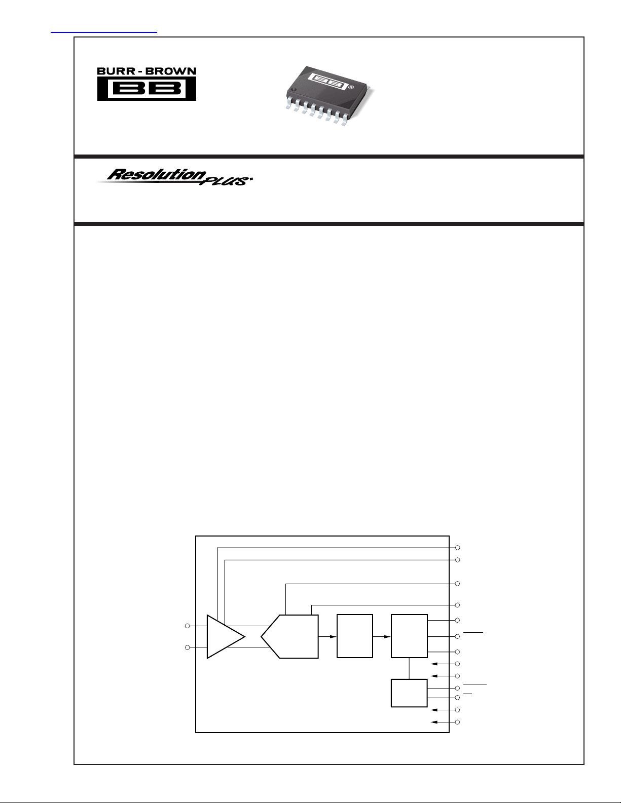
G0
G1
V
REF
CLK
+V
IN
–V
IN
International Airport Industrial Park • Mailing Address: PO Box 11400, Tucson, AZ 85734 • Street Address: 6730 S. Tucson Blvd., Tucson, AZ 85706 • Tel: (520) 746-1111
Twx: 910-952-1111 • Internet: http://www.burr-brown.com/ • Cable: BBRCORP • Telex: 066-6491 • FAX: (520) 889-1510 • Immediate Product Info: (800) 548-6132
©
1999 Burr-Brown Corporation PDS-1520B Printed in U.S.A. December, 1999
PGA
ADS1250
+
–
4th-Order
∆Σ
Modulator
Digital
Filter
Serial
Output
Control
SCLK
DRDY
DOUT
+V
S
AGND
DSYNC
CS
+V
D
DGND
Page 2

SPECIFICATIONS
All specifications at T
PARAMETER CONDITIONS MIN TYP MAX UNITS
ANALOG INPUT
Input Voltage Range
Programmable Gain Amplifier 1 8
Input Impedance (differential) G = Gain 104/G kΩ
Input Capacitance G = Gain 6 • G pF
Input Leakage At +25°C550pA
DYNAMIC CHARACTERISTICS
Data Rate 25 kHz
Bandwidth 3dB 5.4 kHz
Serial Clock (SCLK) 9.6 MHz
System Clock Input (CLK) 9.6 MHz
ACCURACY
Integral Linearity Error
THD 1kHz Input; 0.1dB below FS 97 dB
Noise 2.8 3.8 ppm of FSR, rms
Resolution 20 Bits
No Missing Codes 20 Bits
Common-Mode Rejection
Gain Error 1 % of FSR
Offset Error ±100 ±200 ppm of FSR
Gain Sensitivity to V
Power Supply Rejection Ratio 60 78 dB
PERFORMANCE OVER TEMPERATURE
Offset Drift 0.25 ppm/°C
Gain Drift 5.0 ppm/°C
VOLTAGE REFERENCE
V
REF
Load Current 125 µA
DIGITAL INPUT/OUTPUT
Logic Family CMOS
Logic Level: V
Data Format Binary Two’s Complement
POWER SUPPLY REQUIREMENTS
Operation +4.75 +5 +5.25 VDC
Quiescent Current, Analog V = +5VDC 14 mA
Quiescent Current, Digital V = +5VDC 1 mA
Operating Power 75 100 mW
TEMPERATURE RANGE
Operating –40 +85 °C
Storage –60 +100 °C
NOTES: (1) In order to achieve the converter’s full-scale range, the input must be fully differential. If the input is single-ended (+V
full-scale range is one-half that of the differential range. (2) Applies to full-differential signals. (3) The common-mode rejection test is performed with a 100mV
differential input.
to T
MIN
, VD = VS = +5V, CLK = 9.6MHz, PGA = 1, and V
MAX
= 4.096, unless otherwise specified.
REF
ADS1250U
(1)
(2)
(3)
REF
G = Gain AGND ±V
At T
to T
MIN
MAX
/G V
REF
1nA
±0.0012 ±0.0020 % of FSR
at DC 90 105 dB
V
= 4.096V ±0.1V 1:1
REF
3.996V 4.096 4.196 V
IH
V
IL
V
OH
V
OL
IOH = –500µA +4.5 V
IOL = 500µA 0.4 V
+4.0 +VD + 0.3 V
–0.3 +0.8 V
or –VIN is fixed), then the
IN
®
ADS1250
2
Page 3
ABSOLUTE MAXIMUM RATINGS
Analog Input: Current................................................ ±100mA, Momentary
V
to VD....................................................................................–0.3V to 6V
S
V
to AGND ............................................................................ –0.3V to 6V
S
V
to DGND ............................................................................ –0.3V to 6V
D
AGND to DGND ................................................................................±0.3V
V
REF
Digital Input Voltage to DGND ..................................... –0.3V to V
Digital Output Voltage to DGND .................................. –0.3V to V
Lead Temperature (soldering, 10s) .............................................. +300°C
Power Dissipation (any package) .................................................. 500mW
Voltage ....................................... AGND –0.3V to V
Voltage to AGND ................................................. –0.3V to VS + 0.3V
±10mA, Continuous
+ 0.3V
S
+ 0.3V
D
+ 0.3V
D
This integrated circuit can be damaged by ESD. Burr-Brown
recommends that all integrated circuits be handled with appropriate precautions. Failure to observe proper handling and
installation procedures can cause damage.
Electrostatic discharge can cause damage ranging from
performance degradation to complete device failure. BurrBrown Corporation recommends that all integrated circuits be
ELECTROSTATIC
DISCHARGE SENSITIVITY
handled and stored using appropriate ESD protection
methods.
PACKAGE/ORDERING INFORMATION
PACKAGE SPECIFIED
PRODUCT PACKAGE NUMBER RANGE MARKING NUMBER
DRAWING TEMPERATURE PACKAGE ORDERING TRANSPORT
ADS1250U SOL-16 211 –40°C to +85°C ADS1250U ADS1250U Rails
" " " " " ADS1250U/1K Tape and Reel
NOTE: (1) Models with a slash (/) are available only in Tape and Reel in the quantities indicated (e.g., /1K indicates 1000 devices per reel). Ordering 1000 pieces
of “ADS1250U/1K” will get a single 1000-piece Tape and Reel.
(1)
MEDIA
The information provided herein is believed to be reliable; however, BURR-BROWN assumes no responsibility for inaccuracies or omissions. BURR-BROWN assumes
no responsibility for the use of this information, and all use of such information shall be entirely at the user’s own risk. Prices and specifications are subject to change
without notice. No patent rights or licenses to any of the circuits described herein are implied or granted to any third party. BURR-BROWN does not authorize or warrant
any BURR-BROWN product for use in life support devices and/or systems.
3
ADS1250
®
Page 4
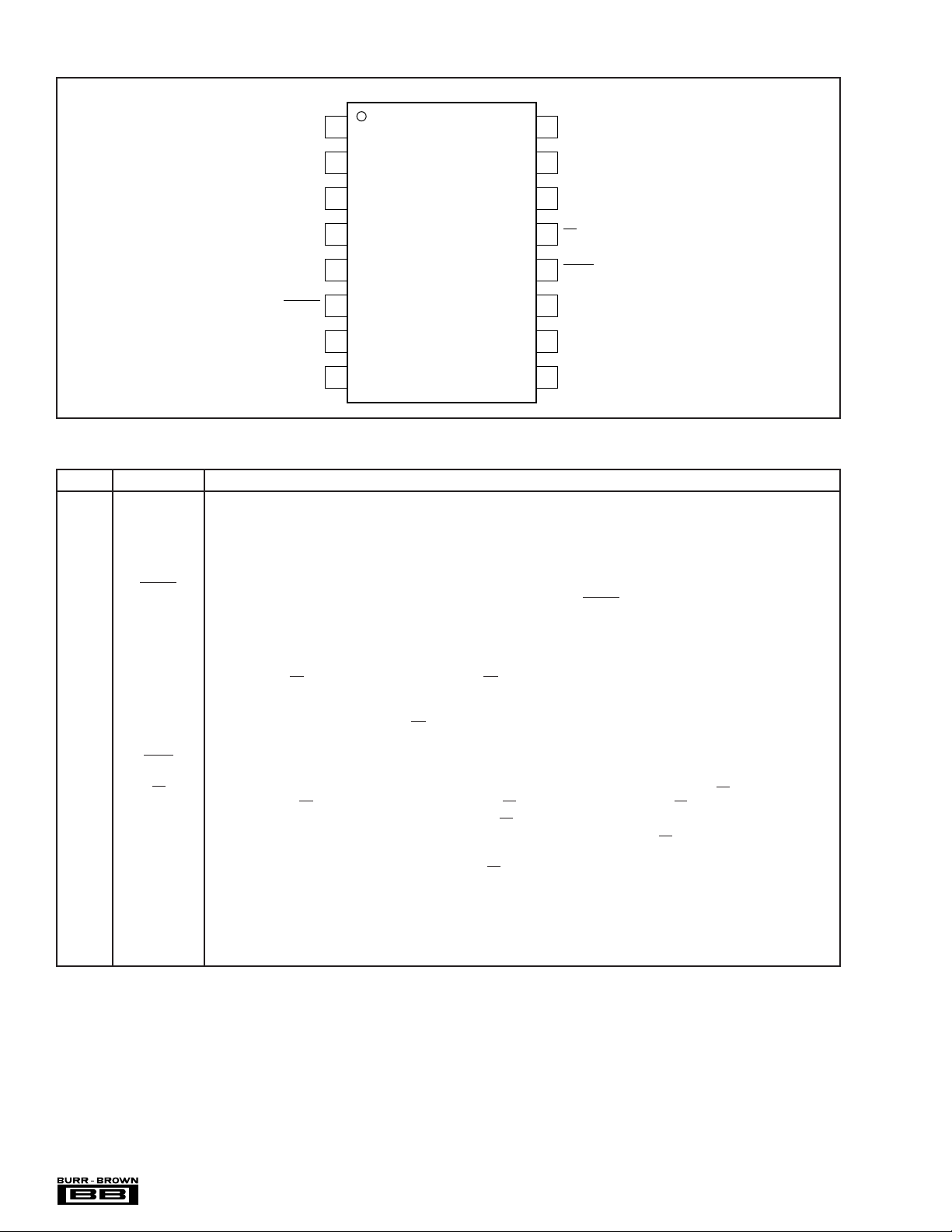
PIN CONFIGURATION
Top View SOL-16
+V
–V
AGND
+V
1
IN
2
IN
3
4
S
16
15
14
13
DGND
G1 (MSB)
G0 (LSB)
CS
ADS1250
V
REF
DSYNC
+V
DGND
5
6
7
D
8
12
DRDY
11
CLK
10
SCLK
9
DOUT
PIN DESCRIPTIONS
PIN NAME PIN DESCRIPTION
1+V
2–V
IN
IN
3 AGND Analog Input: Analog Ground.
4+V
5V
S
REF
6 DSYNC Digital Input: Data Synchronization. A falling edge on this input will reset the modulator count and place the modulator in a hold
7+V
D
8 DGND Digital Input: Digital Ground.
9 DOUT Digital Output: Serial Data Output. The serial data is clocked out of the serial data output shift register through this pin. The pin
10 SCLK Digital Input: Serial Clock. The serial clock is in the form of a CMOS-compatible clock. The serial clock can operate up to the
11 CLK Digital Input: Device System Clock. The system clock is in the form of a CMOS-compatible clock.
12 DRDY Digital Output: Data Ready. A falling edge on this output indicates that a new output word is available from the ADS1250 data output
13 CS Digital Input: Chip Select. Active LOW logic input used to enable serial data output from the ADS1250. CS controls the state of
14 G0 Digital Input: Gain Selection Control (LSB).
15 G1 Digital Input: Gain Selection Control (MSB).
16 DGND Digital Input: Digital Ground.
Analog Input: Positive Input of the Differential Analog Input.
Analog Input: Negative Input of the Differential Analog Input.
Analog Input: Analog Power Supply Voltage, +5V.
Analog Input: Reference Voltage Input.
state. The modulator is released from the hold state on the rising edge of DSYNC. This can be used to synchronize multiple
ADS1250s.
Digital Input: Digital Power Supply Voltage, +5V.
is driven when CS is LOW, and high impedance when CS is HIGH.
device’s system clock frequency. The serial clock can be either a free-running clock or noncontinuous clock, with either type of
clock; the serial data output is gated by CS.
register.
the DOUT pin. If CS is HIGH, DOUT is high impedance; if CS is LOW, DOUT drives the bus. CS can be used in three ways:
(1)If the ADS1250 shares the bus with other devices, CS is used as serial data output enable for communications.
(2)If the ADS1250 shares the bus with other devices and SCLK is a free-running clock, CS is used to gate serial data
out of the device.
(3) If the ADS1250 is the only device on the bus, CS can be tied LOW to always enable serial data output for a
two-wire interface.
Refer to the Serial Communications section of this data sheet for more detail.
®
ADS1250
4
Page 5
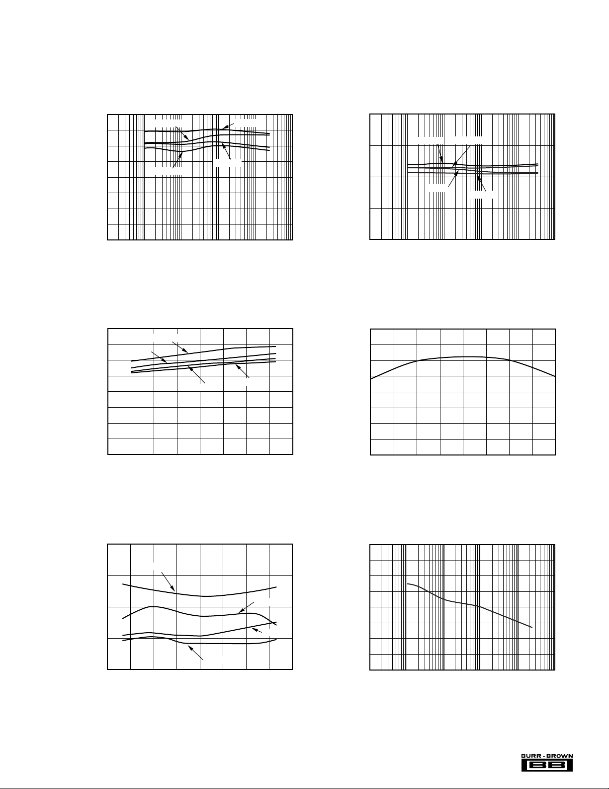
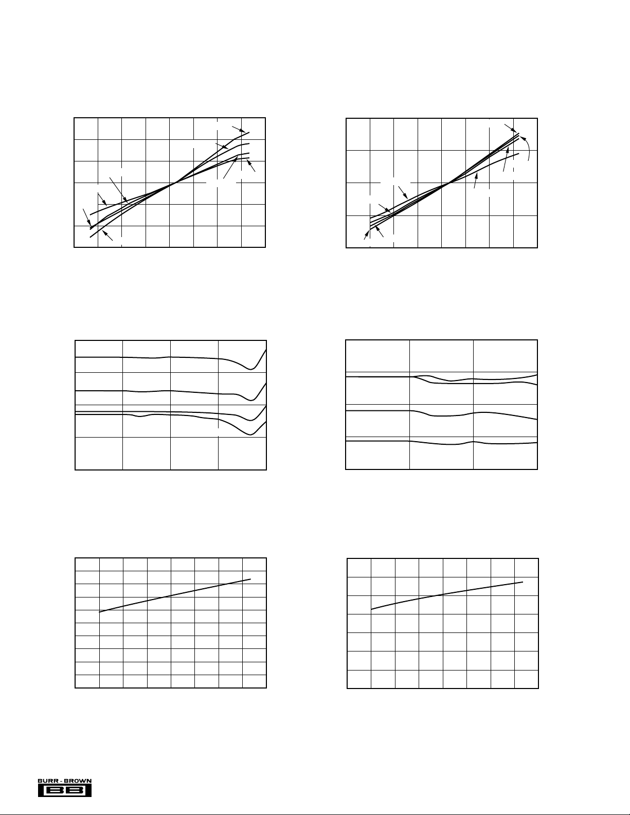
TYPICAL PERFORMANCE CURVES
4.0
3.5
3.0
2.5
2.0
1.5
1.0
0.5
0.0
RMS NOISE vs INPUT VOLTAGE (PGA = 1)
Differential Analog Input Voltage (V)
–4.0 –3.0 –2.0 –1.0 0.0 1.0 2.0 3.0 4.0
RMS Noise (ppm of FS)
EFFECTIVE RESOLUTION
vs DATA OUTPUT RATE
20.0
19.0
18.0
17.0
16.0
10 100 1000 10000 100001
Data Output Rate (Hz)
Effective Resolution Bits (rms)
PGA = 1
PGA = 8
PGA = 2
PGA = 4
At TA = +25°C, VD = VS = +5V, CLK = 9.6MHz, PGA = 1, and V
RMS NOISE vs DATA OUTPUT RATE
4.0
3.5
3.0
2.5
2.0
1.5
1.0
RMS Noise (ppm of FS)
0.5
0.0
10 100 1000 10000 100001
PGA = 4
PGA = 1
Data Output Rate (Hz)
PGA = 8
PGA = 2
= 4.096, unless otherwise specified.
REF
4.0
3.5
3.0
2.5
2.0
1.5
1.0
RMS Noise (ppm of FS)
0.5
0.0
–60 –40 –20 0 20 40 60 80 100
20
15
10
INL (ppm of FS)
5
0
–60 –40 –20 0 20 40 60 80 100
RMS NOISE vs TEMPERATURE
PGA = 8
PGA = 4
Temperature (°C)
INTEGRAL NON-LINEARITY vs TEMPERATURE
PGA = 1
Temperature (°C)
PGA = 2
PGA = 4
PGA = 1
PGA = 2
PGA = 8
5
14.0
13.5
13.0
12.5
12.0
11.5
INL (ppm of FS)
11.0
10.5
10.0
INTEGRAL NON-LINEARITY
vs DATA OUTPUT RATE (PGA = 1)
10 100 1000 10000 100001
Data Output Rate (Hz)
®
ADS1250
Page 6
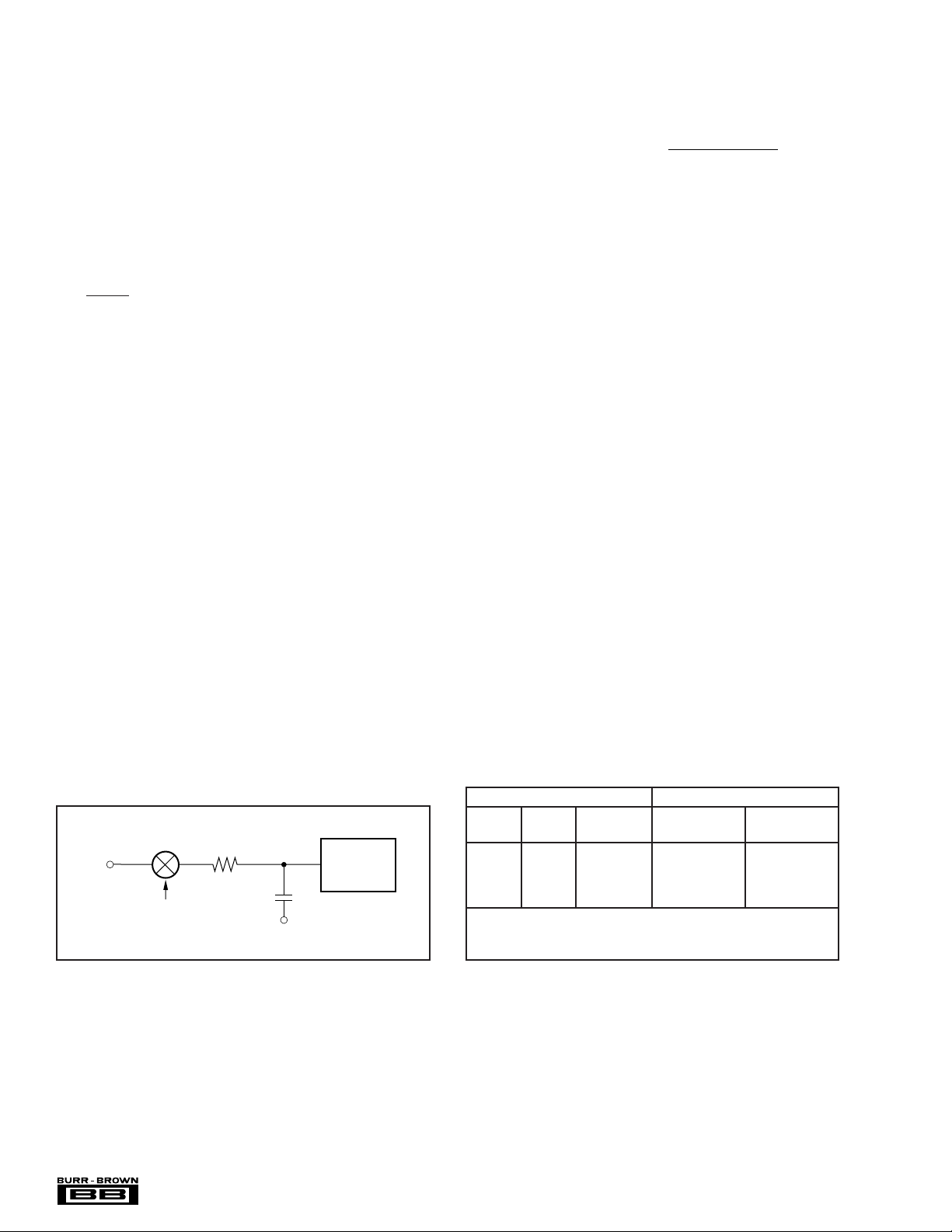
TYPICAL PERFORMANCE CURVES (Cont.)
At TA = +25°C, VD = VS = +5V, CLK = 9.6MHz, PGA = 1, and V
= 4.096, unless otherwise specified.
REF
30
20
10
0
–10
PGA = 4
Offset Drift (ppm of FS)
–20
–30
–60 –40 0–20 4020 60 10080
100
90
80
PSRR (dB)
70
OFFSET DRIFT vs TEMPERATURE
PGA = 8
PGA = 1
PGA = 2
Temperature (°C)
POWER SUPPLY REJECTION RATIO
vs FREQUENCY
PGA = 4
PGA = 2
PGA = 8
PGA = 1
PGA = 1
PGA = 8
PGA = 4
PGA = 2
400
200
0
–200
Gain Drift (ppm of FS)
PGA = 1
–400
–60 –40 0–20 4020 60 10080
120
115
110
CMRR (dB)
105
GAIN DRIFT vs TEMPERATURE
PGA = 8
PGA = 4
PGA = 2
Temperature (°C)
COMMON-MODE REJECTION RATIO
vs FREQUENCY
PGA = 1
PGA = 2
PGA = 4
PGA = 8
PGA = 1
PGA = 2
PGA = 4
PGA = 8
60
1 10 100 1k 10k
Frequency (Hz)
ANALOG CURRENT vs TEMPERATURE
20.0
18.0
16.0
14.0
12.0
10.0
8.0
6.0
Analog Current (mA)
4.0
2.0
0.0
–60 –40 0–20 4020 60 10080
(PGA = 1)
Temperature (°C)
100
1 10 100 1000
Frequency (Hz)
DIGITAL CURRENT vs TEMPERATURE
1.4
1.2
1.0
0.8
0.6
0.4
Digital Current (mA)
0.2
0.0
–60 –40 0–20 4020 60 10080
(PGA = 1)
Temperature (°C)
®
ADS1250
6
Page 7

0
–20
–40
–60
–80
–100
–120
–140
–160
–180
–200
TYPICAL FFT ANALYSIS
OF THE 1kHz f
S
INPUT SIGNAL (PGA = 4)
Frequency (Hz)
0 2500 5000 7500 10000 12500
Dynamic Range (dB)
TYPICAL PERFORMANCE CURVES (Cont.)
At TA = +25°C, VD = VS = +5V, CLK = 9.6MHz, PGA = 1, and V
= 4.096, unless otherwise specified.
REF
POWER DISSIPATION vs CLK FREQUENCY
100
80
60
40
Power Dissipation (mW)
20
0
0.0 2.0 6.04.0 10.08.0
(PGA = 1)
CLK Frequency (MHz)
®
7
ADS1250
Page 8
THEORY OF OPERATION
The ADS1250 is a precision, high dynamic range, 20-bit,
delta-sigma, A/D converter capable of achieving very highresolution digital results at high data rates. The analog input
signal is continuously sampled at a rate determined by the
frequency of the system clock (CLK). The sampled analog
input is modulated by the delta-sigma A/D modulator, followed by a digital filter value. A programmable gain function is also incorporated in the delta-sigma modulator with
larger input sampling capacitors for higher gains. A sinc
digital low-pass filter processes the output of the delta-sigma
modulator and writes the result into the data output register.
The DRDY pin is pulled LOW indicating that new data is
available to be read by the external microcontroller/microprocessor. As shown in the block diagram, the main functional blocks of the ADS1250 are the programmable gain
amplifier, a fourth-order delta-sigma modulator, a digital
filter, control logic, and a serial interface. Each of these
functional blocks is described below.
ANALOG INPUT
The ADS1250 contains a fully differential analog input with
programmable gain. The fully differential switched capacitor architecture provides low system noise, common-mode
rejection of 105dB, and excellent power supply rejection.
The selectable gains on the input are 1, 2, 4, or 8, which
gives a bipolar input voltage range from –4.096 to +4.096V,
to –512mV to +512mV, when the reference input voltage
equals +4.096V. The bipolar ranges are with respect to –V
and not with respect to GND.
Figure 1 shows the basic input structure of the ADS1250.
The analog input impedance is directly related to the sampling frequency of the input capacitor (f
setting (G) of the device. The sampling frequency of the
input capacitor is derived from the system clock (CLK).
Therefore, a lower CLK rate decreases the sampling frequency, which results in a higher analog input impedance.
), and the gain
MOD
Additionally, a lower gain setting (G) decreases the sampling capacitor size, which results in a higher analog input
impedance. This can be seen in the following equation:
A Impedance ( )
IN
Ω=
9.6 MHz 104E3
•
CLK G
•
With regard to the analog input signal, the overall analog
performance of the device is affected by three items. First,
the input impedance can affect accuracy. If the source
5
impedance of the input signal is significant, or if there is
passive filtering prior to the ADS1250, a significant portion
of the signal can be lost across this external impedance. The
magnitude of the effect is dependent on the desired system
performance.
Second, the current into or out of the analog inputs must be
limited. Under no conditions should the current into or out
of the analog inputs exceed 10mA.
Third, to prevent aliasing of the input signal, the bandwidth
of the analog input signal must be band limited. The bandwidth is a function of the system clock frequency. With a
system clock frequency of 9.6MHz, the data output rate is
25kHz, with a –3dB frequency of 5.4kHz. The –3dB frequency scales with the system clock frequency.
To guarantee the best linearity of the ADS1250, a fully
differential signal is recommended.
PROGRAMMABLE GAIN AMPLIFIER
IN
The PGA gain setting is programmed via the PGA pins on the
ADS1250. Changes in the gain setting (G) of the PGA results
in an increase in the input capacitor size. Therefore, higher
gain settings result in a lower analog input impedance.
The PGA of the ADS1250 can be set to a gain of 1, 2, 4, or
8, substantially increasing the dynamic range of the converter
and simplifying the interface to the more common transducers
(see Table I).
R
SW
(1kΩ typical • G)
A
IN
Modulator Frequency
= f
MOD
FIGURE 1. Analog Input Structure.
®
ADS1250
C
INT
(6pF typical • G)
V
CM
Internal
Circuitry
GAIN SETTING
G1 G0 GAIN VALUE FSR (V) FSR (V)
0 0 1 8.192 4.096
0 1 2 4.096 2.048
1 0 4 2.048 1.024
1 1 8 1.024 0.512
NOTE: Based on a 4.096V reference. The ADS1250 allows commonmode voltage as long as the absolute input voltage on +V
not go below AGND or above +V
.
S
ANALOG INPUT
DIFFERENTIAL SINGLE-ENDED
TABLE I. Full-Scale Range versus PGA Setting.
8
or –VIN does
IN
Page 9

DELTA-SIGMA MODULATOR
The modulator clock is generated by dividing the system
clock by 6. With a nominal system clock frequency of
9.6MHz, the modulator clock frequency is 1.6MHz
(9.6MHz / 6). The output from the modulator is oversampled
64 times by the digital filter. Therefore, with 1.6MHz
modulator clock (derived from a 9.6MHz system clock), the
data output rate is 25kHz (1.6MHz / 64). The data output
rate scales directly with the system clock frequency, as
shown in Table II.
CLK (MHz) DATA OUTPUT RATE (Hz)
9.600000 25,000
(1)
7.372800
(1)
6.144000
(1)
6.000000
(1)
4.915200
(1)
3.686400
(1)
3.072000
(1)
2.457600
(1)
1.843200
0.921600 2,400
0.460800 1,200
0.384000 1,000
0.192000 500
0.038400 100
0.023040 60
0.019200 50
0.011520 30
0.009600 25
0.007680 20
0.006400 16.67
0.005760 15
0.004800 12.50
0.003840 10
NOTE: (1) Standard Clock Oscillator.
19,200
16,000
15,625
12,800
9,600
8,000
6,400
4,800
TABLE II. CLK Rate versus Data Output Rate.
REFERENCE INPUT
Unlike the analog input, the reference input impedance has no
dependency on the PGA gain setting.
Reference input takes an average current of 125µA with a
9.6MHz system clock. This current will be proportional to
the system clock. A buffered reference is needed for
ADS1250. The recommended reference circuit is shown in
Figure 2.
Reference voltages higher than 4.096V will increase the
full-scale range, while the absolute internal circuit noise of
the converter remains the same. This will decrease the noise
in terms of ppm of full scale. However, using a higher
reference voltage will also degrade linearity. Therefore, the
use of a higher reference voltage is not recommended.
Reference voltages lower than 4.096V will decrease the fullscale range, while the absolute internal circuit noise at the
converter remains the same. This will increase the noise in
terms of ppm of full scale. However, using a lower reference
voltage will not degrade linearity. Therefore, the use of a
lower reference voltage will reduce the effective resolution.
DIGITAL FILTER
The digital filter is a sinc5 and is described by the following
transfer function:
••
f
f
MOD
f
MOD
•
f
Hf
()
ππ64
sin
=
64
•sin
5
or
5
–
64
z
–
1
z
Hz
()
=
1
–
64 1
•–
()
The digital filter of the ADS1250 computes the digital result
based on the most recent outputs from the delta-sigma
modulator. At the most basic level, the digital filter can be
thought of as simply averaging the modulator results in a
weighted form and presenting this average as the digital
result. The digital result is calculated from the digital filter
every 64 modulator clock cycles, or 6 • 64 = 384 system
clock cycles (refer to the Delta-Sigma Modulator section).
However, if there is a significant change in the analog input,
five full conversions are needed for the digital filter to settle.
If the analog input change occurs asynchronously to the
DRDY pulse, six conversions are needed for the conversion
to fully settle. Furthermore, the group delay is only 2.5
conversions due to the digital filter's linear phase response.
2
3
+5V
0.10µF
7
OPA350
4
6
+
10µF
0.1µF
To V
REF
Pin 5 of
the ADS1250
+5V
1
4.99kΩ
10kΩ
LM404-4.1
+
10µF
0.10µF
FIGURE 2. Recommended External Voltage Reference Circuit for Best Low Noise Operation with the ADS1250.
9
ADS1250
®
Page 10
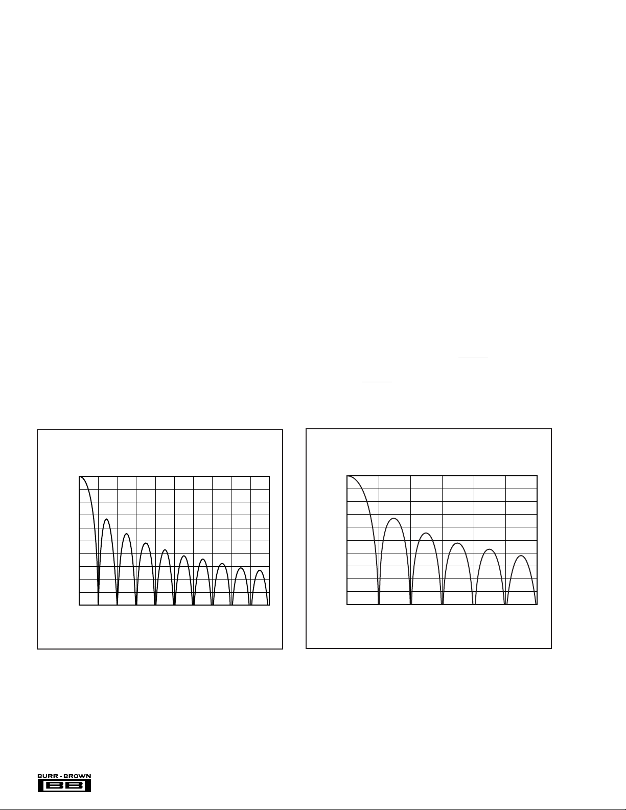
The digital output rate, or data rate, scales directly with the
system CLK frequency. This allows the data output rate to
be changed over a very wide range (five orders of magnitude) by changing the system CLK frequency. However, it
is important to note that the –3dB point of the filter is 0.216
times the data output rate. Therefore, the data output rate
should allow for sufficient margin to prevent attenuation of
the signal of interest.
Since the conversion result is essentially an average, the data
output rate determines the location of the resulting notches
in the digital filter (see Figure 3). Note that the first notch is
located at the data output rate frequency, and subsequent
notches are located at integer multiples of the data output
rate to allow for rejection of not only the fundamental
frequency, but also harmonic frequencies. In this manner,
the data output rate can be used to set specific notch
frequencies in the digital filter response.
For example, if rejection of the power line frequency is
desired, the data output rate can simply be set to the power
line frequency. For 50Hz rejection, the system CLK frequency should be 19.200kHz; this will set the data output
rate to 50Hz (see Table II and Figure 4). For 60Hz rejection,
the system CLK frequency should be 23.040kHz; this will
set the data output rate to 60Hz (see Table II and Figure 5).
If both 50Hz and 60Hz rejection is required, then the system
CLK should be 3.840kHz; this will set the data output rate
to 10Hz and reject both 50Hz and 60Hz (See Table II and
Figure 6).
There is an additional benefit in using a lower data output
rate. It will provide better rejection of signals in the frequency band of interest. For example, with a 50Hz data
output rate, a significant signal at 75Hz may alias back into
the passband at 25Hz. This is due to the fact that rejection at
75Hz may only be 66dB in the stopband (frequencies higher
than the first notch frequency), as shown in Figure 4.
However, setting the data output rate to 10Hz will provide
135dB rejection at 75Hz (see Figure 6). A similar benefit is
gained at frequencies near the data output rate (see Figures
7, 8, 9, and 10). If a slower data output rate does not meet
the system requirements, the analog front end can be designed to provide the needed attenuation to prevent aliasing.
Additionally the data output rate may be increased and
additional digital filtering may be done in the processor or
controller.
CONTROL LOGIC
The control logic is used for communications and control of
the ADS1250.
Power-Up Sequence
Prior to power-up, all digital and analog input pins must be
LOW. At the time of power-up, these signal inputs can be
biased to a voltage other than 0V, however, they should
never exceed +VS or +VD.
Once the ADS1250 powers up, the DRDY line will pulse
LOW on the first conversion. This data will not be valid. The
sixth pulse of DRDY will be valid data from the analog input
signal.
0
–20
–40
–60
–80
–100
–120
Gain (dB)
–140
–160
–180
–200
NORMALIZED DIGITAL FILTER RESPONSE
123456789100
Frequency (Hz)
0
–20
–40
–60
–80
–100
–120
Gain (dB)
–140
–160
–180
–200
DIGITAL FILTER RESPONSE
50 100 150 200 250 3000
Frequency (Hz)
FIGURE 3. Normalized Digital Filter Response. FIGURE 4. Digital Filter Response (50Hz).
®
ADS1250
10
Page 11

0
DIGITAL FILTER RESPONSE
0
–20
–40
–60
–80
–100
–120
–140
–160
–180
–200
10 20 30 40 50 60 70 80 90 1000
Frequency (Hz)
Gain (dB)
–20
–40
–60
–80
–100
–120
Gain (dB)
–140
–160
–180
–200
DIGITAL FILTER RESPONSE
50 100 150 200 250 3000
Frequency (Hz)
FIGURE 5. Digital Filter Response (60Hz). FIGURE 6. Digital Filter Response (10Hz Multiples).
0
–20
–40
–60
–80
–100
–120
Gain (dB)
–140
–160
–180
–200
46 47 48 49 50 51 52 53 54 5545
DIGITAL FILTER RESPONSE
Frequency (Hz)
FIGURE 7. Expanded Digital Filter Response (50Hz with a
50Hz Notch).
0
–20
–40
–60
–80
–100
–120
Gain (dB)
–140
–160
–180
–200
56 57 58 59 60 61 62 63 64 6555
DIGITAL FILTER RESPONSE
Frequency (Hz)
FIGURE 9. Expanded Digital Filter Response (60Hz with a
60Hz Notch).
0
–20
–40
–60
–80
–100
–120
Gain (dB)
–140
–160
–180
–200
46 47 48 49 50 51 52 53 54 5545
DIGITAL FILTER RESPONSE
Frequency (Hz)
FIGURE 8. Expanded Digital Filter Response (50Hz with a
10Hz Notch).
0
–20
–40
–60
–80
–100
–120
Gain (dB)
–140
–160
–180
–200
56 57 58 59 60 61 62 63 64 6555
DIGITAL FILTER RESPONSE
Frequency (Hz)
FIGURE 10. Expanded Digital Filter Response (60Hz with
a 10Hz Notch).
11
ADS1250
®
Page 12

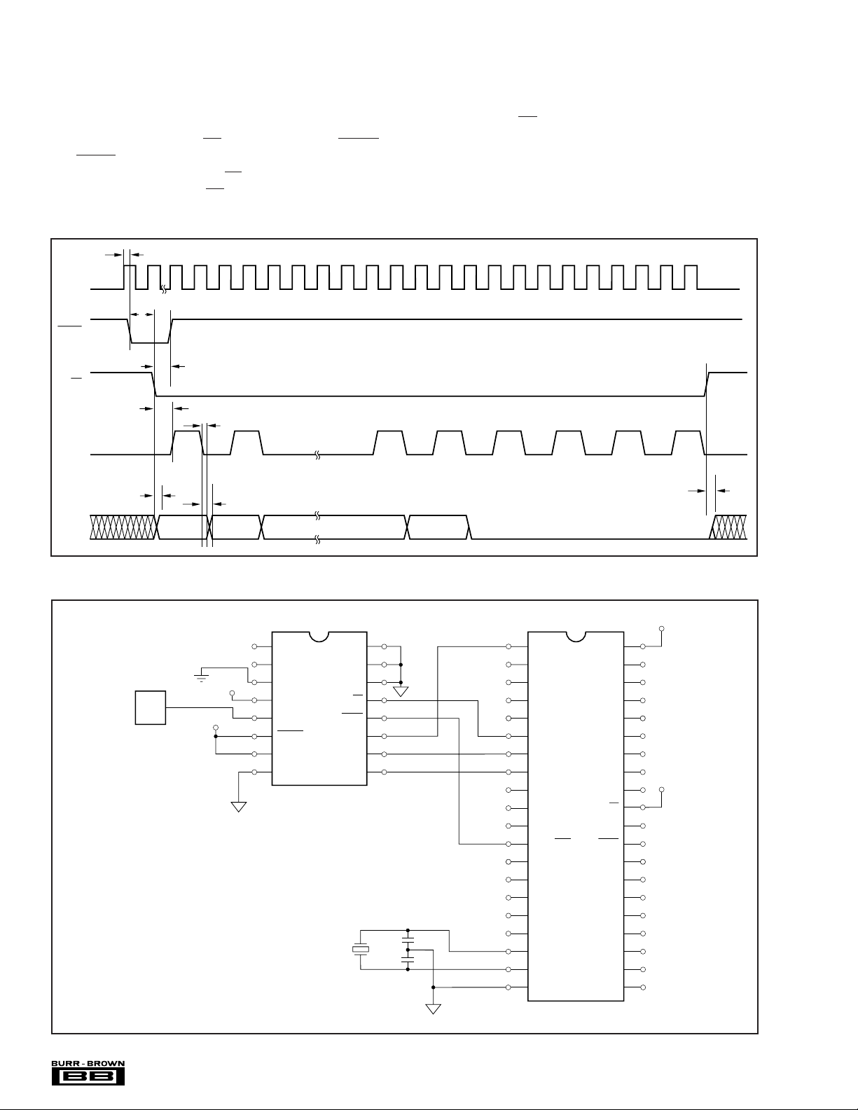
DSYNC
The DSYNC signal can be used is two ways. First, DSYNC
can be used to synchronize multiple converters. This is done
by applying a negative-going pulse on DSYNC. The negative pulse resets the current modulator count to zero and
places it in a hold state. The modulator is released from the
hold state and synchronization occurs on the rising edge of
DSYNC. DSYNC does not reset the internal data to zero.
Synchronization assumes that each ADS1250 is driven from
the same system clock. If the DSYNC pulse is completely
asynchronous to the master clock, some ADS1250s may
start-up one CLK clock cycle before the others.
CLK
t
14
t
13
DSYNC
FIGURE 11. DSYNC to CLK Timing for Synchronizing
Multiple ADS1250s.
Therefore, the output data will be synchronized, but only to
within one CLK clock cycle. To ensure exact synchronization to the same CLK clock edge, the timing relationship
between the DSYNC and CLK signals must be observed, as
shown in Figure 11 and Table III. Figure 12 shows a simple
circuit which can be used to clock multiple ADS1250s from
one ADS1250, as well as to ensure that an asynchronous
DSYNC signal will exactly synchronize all the converters.
The second use of DSYNC is to reset the modulator count
to zero in order to obtain valid data as quickly as possible.
For example, if the analog input signal is changed significantly on the ADS1250, the current conversion cycle will be
a mix of the old data and the new data. Five conversions are
needed for the digital filter to settle. Therefore, the sixth
conversion will be valid data. However, if the analog input
signal is changed and then DSYNC is used to reset the
modulator count, the modulator data at the end of the current
conversion cycle will be entirely from the new signal. After
four additional conversion cycles, the output data will be
completely valid. Note that the conversion cycle in which
DSYNC is used will be slightly longer than normal. Its
length will depend on when DSYNC was set.
Asynchronous
DSYNC
Strobe
DV
DD
OSC
DGND
1/6 74AHC04
1/2 74AHC74
D
CLK
DSYNC
CLK
DGND
ADS1250
Q
Q
DOUT
SCLK
DV
DSYNC
CLK
DD
DGND
ADS1250
DOUT
SCLK
DV
DD
DSYNC
CLK
DGND
ADS1250
DOUT
SCLK
DV
DD
FIGURE 12. Exactly Synchronizing Multiple ADS1250s to an Asynchronous DSYNC Signal.
SYMBOL DESCRIPTION MIN TYP MAX UNITS
t
1
t
2
t
3
t
4
t
5
t
6
t
7
t
8
t
9
t
10
t
11
t
12
t
13
t
14
DOR Write Time (Using CS) 6 • CLK ns
DRDY LOW Time 6 • CLK ns
DOR Write Time (CS HIGH) 6 • CLK ns
DRDY HIGH Time 6 • CLK ns
Rising Edge of CLK to Falling Edge of DRDY 30 ns
Falling Edge of DRDY to Falling Edge of CS 30 ns
Falling Edge of CS to Rising Edge of DRDY 6 • CLK ns
Falling Edge of CS to Rising Edge of SCLK or
Falling Edge of DRDY to Rising Edge of SCLK if CS is Tied LOW 30 ns
Falling Edge of CS to DOUT Valid or
Falling Edge of DRDY to DOUT Valid if CS is Tied LOW (Setup Time) 30 ns
Falling Edge of SCLK to DOUT Valid (Hold Time) 5 ns
Falling Edge of SCLK to Next DOUT Valid (Setup Time) 30 ns
Rising Edge of CS to DOUT High Impedance 30 ns
DSYNC Pulse Width 100 ns
Falling Edge of CLK to Falling Edge of DSYNC – 5 ns
CLK
2
TABLE III. Digital Timing.
®
ADS1250
12
Page 13

CS
The CS signal controls the state of DOUT. If CS is HIGH,
DOUT is in a high-impedance state. When CS is LOW,
DOUT drives the bus.
DRDY
The DRDY signal is used to indicate that new data has been
loaded into the data output register and is ready to be read.
The operation of DRDY depends on how the CS signal is
used. The specifics of the three communications methods
are described in the Serial Interface section.
In the first case, which is typical for three-wire serial
communications (CS tied LOW), DRDY would normally be
HIGH. The result of the A/D conversion would be written to
the DOR from MSB to LSB in the time defined by t1. The
DRDY line would then pulse LOW for time defined by t2,
as shown in Figure 13.
MSB to LSB in the time defined by t3. The DRDY line
would stay HIGH for the time defined by t4, as shown in
Figure 15.
DRDY
MSB
written
to DOR
t
3
complete
DOR
write
t
4
FIGURE 15. DRDY Pulse (CS HIGH).
Reading DRDY during the time shown by t1 and t3 (Figures
13, 14, and 15) will result in invalid data being read. This is
due to the fact that writes to the DOR are not blocked.
Subsequently, a read from DOR during this time will result
in a combination of old and new data.
t
2
DRDY
DOUT
MSB
written
to DOR
t
1
DOR
write
complete
FIGURE 13. DRDY Pulse (CS tied LOW).
In the second case, which is typical for four-wire serial
communications (CS used), DRDY would normally be HIGH.
The result of the A/D conversion would be written to the DOR
from MSB to LSB in the time defined by t1. The DRDY would
go LOW after the DOR write is completed. After taking CS
LOW, the DRDY line would remain LOW for the time
defined by t2, as shown in Figure 14.
t
2
DRDY
CS
DOUT
MSB
written
to DOR
t
1
DOR
write
complete
FIGURE 14. DRDY Pulse (using CS).
In the third case, CS is left HIGH, which may be used if data
is only periodically read from the ADS1250. In this case,
DRDY would normally be LOW. DRDY would go HIGH
immediately prior to the MSB being written to the DOR.
The result of the A/D conversion would be written from
SERIAL INTERFACE
The ADS1250 includes a simple serial interface which can
be connected to microcontrollers and digital signal processors in a variety of ways. Communications with the ADS1250
can commence on the first detection of the DRDY pulse
after power up, although data will not be valid until the sixth
conversion.
It is important to note that the data from the ADS1250 is a 20bit result transmitted MSB-first in Binary Two’s Complement
format, as shown in Table IV.
DIFFERENTIAL VOLTAGE INPUT DIGITAL OUTPUT (HEX)
+Full Scale 7FFFFH
Zero 00000H
–Full Scale 80000H
TABLE IV. ADS1250 Data Format (Binary Two's Comple-
ment).
The entire 20-bit result can be read out of the device by simply
providing 20 SCLKs during serial communication with the
part. However, the most common method of communicating
with the device is with a standard SSI interface, such as SPI.
This protocol is based on 8-bit or 16-bit data transfers. It is
possible to use a standard 8-bit or 16-bit data transfer with the
ADS1250. For instance, if only 16 bits of data are read, the
internal bit pointer will automatically reset to the MSB of the
DOR on the next DRDY pulse. This will ensure that the next
read from the DOR will begin with the MSB of newly
converted data. If more than 20 bits of data are read, the data
will be 0 padded. Therefore, if 24 bits of data are read from the
ADS1250, the lowest four bits of the 24-bit data transfer are
read as 0s (0 padded).
The only limitation on SCLK is that it cannot be higher than
9.6MHz. Therefore, it is possible to run CLK at a lower
frequency than SCLK. For instance, it is possible to run
CLK at 23.040kHz for a 60Hz notch, and run SCLK at
9.6MHz to achieve high-speed serial communications. Additionally, the data must be clocked out before the next
DRDY to ensure valid data, as described in the DRDY
section.
13
ADS1250
®
Page 14
There are three basic methods of receiving data from the
ADS1250. The first two methods involve a four-wire interface and the third method is a three-wire interface.
Method 1: Four-Wire Interface
The most common method of receiving data is using a
simple four-wire interface (CS, SCLK, DOUT, and DRDY).
The DRDY line will pulse LOW after the DOR is updated.
The processor would then take CS LOW to select the device
for communication. Once CS is taken LOW, the DOUT
would be driven to the level dictated by the MSB of the data
t
5
CLK
t
6
DRDY
t
7
CS
t
8
t
10
SCLK
12 19
output register. The processor would provide 20 (or 24)
SCLKs to read the contents of the DOR. The data bits in the
DOR are shifted out on the DOUT pin after the falling edge
of SCLK. If more than 20 bits of data are read, the data is 0
padded. Taking CS HIGH will take DOUT to a highimpedance state. The timing for the data transfer is shown in
Figure 16 (see Table III). A simple four-wire interface using
this method is shown in Figure 17. The P1.0 output from the
8xC51 is a free-running clock.
20 21 22 23 24
t
DOUT
OUT
MSB
9
t
11
OUT
LSB
FIGURE 16. Method 1: Four-Wire Interface Using Noncontinuous SCLK.
V
REF
Circuit
AGND
+V
IN
–V
IN
AV
DD
DV
DD
DGND
AGND
+V
S
V
REF
DSYNC
+V
D
DGND
ADS1250
DGND
DRDY
CLK
SCLK
DOUT
G1
G0
CS
XTAL
DGND
C1
C2
P1.0 / T2
P1.1
P1.2
P1.3
P1.4
P1.5
P1.6
P1.7
RST
P3.0
P3.1
P3.2 / INT0
P3.3
P3.4
P3.5
P3.6
P3.7
XTAL2
XTAL1
V
SS
8xC51
V
P0.0
P0.1
P0.2
P0.3
P0.4
P0.5
P0.6
P0.7
ALE
PSEN
P2.7
P2.6
P2.5
P2.4
P2.3
P2.2
P2.1
P2.0
t
12
DV
DD
CC
DV
DD
EA
FIGURE 17. Four-Wire Interface to an 8xC51.
®
ADS1250
DGND
14
Page 15

Method 2: Four-Wire Interface
The second method of receiving data also uses a simple
four-wire interface (CS, SCLK, DOUT, and DRDY). The
main difference from method 1 is that SCLK is a freerunning clock. The DRDY line will pulse LOW for the time
defined by t2 after the DOR is updated. The processor would
then take CS LOW to select the device for communication.
The recommended method of using CS is to take CS LOW
on the falling edge of SCLK. The only timing constraint of
CS is that the setup time (t9) for the data must be met before
the rising edge of SCLK. Once CS is taken LOW, the DOUT
t
5
CLK
t
6
DRDY
t
7
CS
t
8
t
10
SCLK
12
would be driven to the level dictated by the MSB of the data
output register. CS would be held low for 20 (or 24) SCLKs
to read the contents of the DOR. The data bits in the DOR
are shifted out on the DOUT pin after the falling edge of
SCLK. If CS is held low for more than 20 SCLKs, the data
would be 0 padded. Taking CS HIGH will take DOUT to a
high-impedance state. The timing for the data transfer is
shown in Figure 18 (see Table III). A simple four-wire
interface is shown in Figure 19. The P1.0 output from the
8xC51 is a free-running clock.
19
20 21 22 23 24
t
DOUT
9
OUT
MSB
t
11
OUT
LSB
FIGURE 18. Method 2: Four-Wire Interface Using a Free-Running SCLK.
V
REF
Circuit
AGND
+V
IN
–V
IN
AV
DD
DV
DD
DGND
AGND
+V
S
V
REF
DSYNC
+V
D
DGND
ADS1250
DGND
DRDY
CLK
SCLK
DOUT
G1
G0
CS
XTAL
DGND
C1
C2
P1.0 / T2
P1.1
P1.2
P1.3
P1.4
P1.5
P1.6
P1.7
RST
P3.0
P3.1
P3.2 / INT0
P3.3
P3.4
P3.5
P3.6
P3.7
XTAL2
XTAL1
V
SS
8xC51
V
P0.0
P0.1
P0.2
P0.3
P0.4
P0.5
P0.6
P0.7
ALE
PSEN
P2.7
P2.6
P2.5
P2.4
P2.3
P2.2
P2.1
P2.0
t
12
DV
DD
CC
DV
DD
EA
DGND
FIGURE 19. Four-Wire Interface to an 8xC51 (Free-Running SCLK).
15
®
ADS1250
Page 16

Method 3: Three-Wire Interface
The third method of receiving data uses a simple three-wire
interface (SCLK, DOUT, and DRDY). The main difference
from method 1 is that CS is tied LOW, therefore, the DOUT
pin is always driving the bus. The DRDY line will pulse
LOW after the DOR is updated. Since CS is tied LOW (the
DOUT pin is enabled for output), the level dictated by the
MSB of the data output register would be driven on the bus.
The processor would provide 20 (or 24) SCLKs to read the
contents of the DOR. The data bits in the DOR are shifted
out on the DOUT pin after the falling edge of SCLK. If more
t
5
CLK
t
2
DRDY
t
8
SCLK
12 19
than 20 bits of data are read, the data is 0 padded. Since CS
is tied LOW, the bus will be driven to the state of the last bit
that was shifted out of the DOR. The timing for the data
transfer is shown in Figure 20 (see Table III). A simple
three-wire interface using this method is shown in Figure 21.
The P1.0 output from the 8xC51 is a free-running clock.
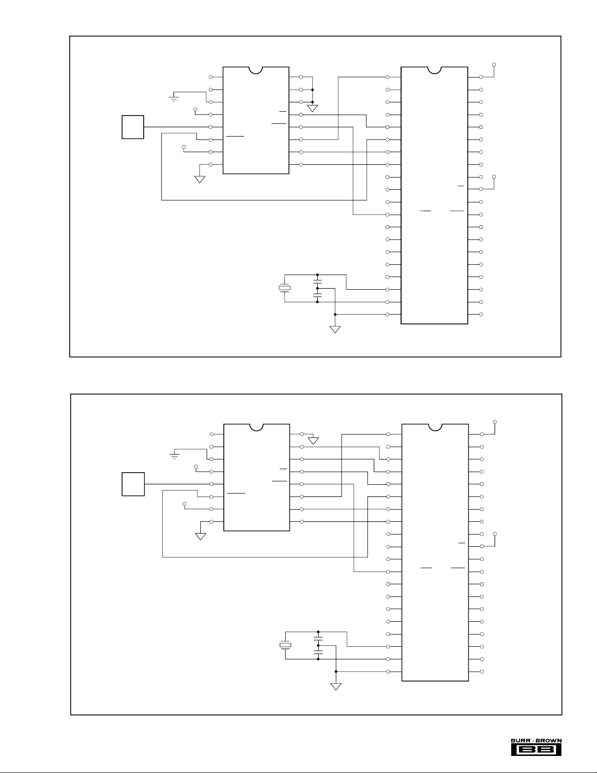
Figure 22 shows a five-wire interface using DSYNC. The
communication with the ADS1250 is the same as described
in Method 1. Figure 23 shows a full interface using DSYNC,
G1, and G0. The communication with ADS1250 is the same
as described in Method 1.
t
10
20 21 22 23 24
t
9
DOUT
OUT
MSB
FIGURE 20. Method 3: Two-Wire Interface (CS tied LOW).
V
REF
Circuit
AGND
+V
IN
–V
IN
AV
DD
DV
DD
DGND
AGND
+V
S
V
REF
DSYNC
+V
D
DGND
ADS1250
DGND
G1
G0
CS
DRDY
CLK
SCLK
DOUT
XTAL
DGND
C1
C2
t
11
OUT
LSB
P1.0 / T2
P1.1
P1.2
P1.3
P1.4
P1.5
P1.6
P1.7
RST
P3.0
P3.1
P3.2 / INT0
P3.3
P3.4
P3.5
P3.6
P3.7
XTAL2
XTAL1
V
SS
8xC51
V
P0.0
P0.1
P0.2
P0.3
P0.4
P0.5
P0.6
P0.7
ALE
PSEN
P2.7
P2.6
P2.5
P2.4
P2.3
P2.2
P2.1
P2.0
DV
DD
CC
DV
DD
EA
FIGURE 21. Three-Wire Interface to an 8xC51 (CS tied LOW).
®
ADS1250
16
DGND
Page 17
8xC51
DV
DD
V
REF
Circuit
AGND
+V
IN
–V
IN
AV
DD
DV
DD
AGND
+V
S
V
REF
DSYNC
+V
D
DGND
ADS1250
DGND
G1
G0
CS
DRDY
CLK
SCLK
DOUT
DGND
P1.0 / T2
P1.1
P1.2
P1.3
P1.4
P1.5
P1.6
P1.7
RST
DGND
P3.0
P3.1
P3.2 / INT0
P3.3
P3.4
P3.5
P3.6
P3.7
XTAL2
XTAL1
V
SS
XTAL
C1
C2
V
P0.0
P0.1
P0.2
P0.3
P0.4
P0.5
P0.6
P0.7
ALE
PSEN
P2.7
P2.6
P2.5
P2.4
P2.3
P2.2
P2.1
P2.0
CC
DV
DD
EA
DGND
FIGURE 22. Five-Wire Interface to an 8xC51.
+V
IN
–V
IN
AGND
+V
S
V
REF
DSYNC
+V
D
DGND
ADS1250
V
REF
Circuit
AGND
AV
DD
DV
DD
DGND
DGND
DRDY
CLK
SCLK
DOUT
DV
8xC51
G1
DGND
G0
CS
P1.1
P1.2
P1.3
P1.4
P1.5
P1.6
P1.7
RST
P3.0
P3.1
P3.2 / INT0
P3.3
P3.4
P3.5
P3.6
P1.0 / T2
P3.7
XTAL2
XTAL1
V
SS
XTAL
C1
C2
V
P0.0
P0.1
P0.2
P0.3
P0.4
P0.5
P0.6
P0.7
EA
ALE
PSEN
P2.7
P2.6
P2.5
P2.4
P2.3
P2.2
P2.1
P2.0
CC
DD
DV
DD
FIGURE 23. Full Interface to an 8xC51.
17
DGND
®
ADS1250
Page 18

SOFTWARE GAIN
The excellent performance, flexibility, and low cost of the
ADS1250 allows the converter to be considered for designs
which would not normally need a 20-bit ADC. For example,
many designs utilize a 12-bit converter and a high gain INA
or PGA for digitizing low amplitude signals. For some of these
applications, the ADS1250 by itself may be a solution. The
digital result of the converter can simply be shifted up by “n”
bits in the main controller, resulting in a gain of “n” times G,
where G is the gain setting. While this type of manipulation of
the output data is obvious, it is easy to miss how much the gain
can be increased in this manner on a 20-bit converter. For
example, shifting the result by 4 bits when the ADS1250 is set
to a gain of 8 results in an effective gain of 128.
Isolation
The serial interface of the ADS1250 provides for simple
isolation methods. An example of an isolated four-wire
interface is shown in Figure 19. The ISO150 is used to
transmit the digital clocks over the isolation barrier. In
addition, the digital output of the ADS1250 can, in some
cases, drive opto-isolators directly. Note that DOUT is tristated for the majority of the conversion period and the optoisolator connection must take this into account.
V
DD2
DRDY
DGND
2A
R/T
A
G
2BD2B
SB
V
R/T
2A
D
V
REF
Circuit
AGND
ISO150
1A
D
+V
IN
–V
IN
AV
DD
V
DD1
DGND
AGND
+V
S
V
REF
DSYNC
+V
D
DGND
ADS1250
DGND
G1
G0
CS
DRDY
CLK
SCLK
DOUT
DGND
2A
D
1A
D
R/T1AV
DGND
V
DD1
R/T
R/T1AV
DGND
SA
V
DD1
DGND
A
2A
G
ISO150
SA
V
DD1
AGND
AGND
GBR/T1BD
V
DD2
SB
V
GBR/T1BD
V
V
1B
CLK
DD2
DGND
SCLK
2BD2B
R/T
1B
DOUT
DD2
FIGURE 24. Isolated Four-Wire Interface.
®
ADS1250
18
Page 19

LAYOUT
POWER SUPPLIES
The analog supply should be well regulated and low noise.
For designs requiring very high resolution from the ADS1250,
power supply rejection will be a concern. Avoid running
digital lines under the device as they may couple noise onto
the die. The requirements for the digital supply are not as
strict, however, high frequency noise on VD can capacitively
couple into the analog portion of the ADS1250. This noise
can originate from switching power supplies, very fast
microprocessors, or digital signal processors. For either
supply, high frequency noise will alias back into the passband of the digital filter, affecting the conversion result. If
one supply must be used to power the ADS1250, the V
supply should be used to power VD. This connection can be
made via a 10Ω resistor which, along with the decoupling
capacitors, will provide some filtering between VD and VS.
In some systems, a direct connection can be made. Experimentation may be the best way to determine the appropriate
connection between VS and VD.
GROUNDING
The analog and digital sections of the design should be
carefully and cleanly partitioned. Each section should have
its own ground plane with no overlap between them. AGND
should be connected to the analog ground plane as well as all
other analog grounds. DGND should be connected to the
digital ground plane and all digital signals referenced to this
plane. The ADS1250 pinout is such that the converter is
cleanly separated into an analog and digital portion. This
should allow simple layout of the analog and digital sections
of the design. For a single converter system, AGND and
DGND of the ADS1250 should be connected together,
underneath the converter. Do not join the ground planes, but
connect the two with a moderate signal trace. For multiple
converters, connect the two ground planes at one location as
central to all of the converters as possible. In some cases,
experimentation may be required to find the best point to
connect the two planes together. The printed circuit board
can be designed to provide different analog/digital ground
S
connections via short jumpers. The initial prototype can be
used to establish which connection works best.
DECOUPLING
Good decoupling practices should be used for the ADS1250
and for all components in the design. All decoupling capacitors, but specifically the 0.1µF ceramic capacitors, should be
placed as close as possible to the pin being decoupled. A
1µF to 10µF capacitor, in parallel with a 0.1µF ceramic
capacitor, should be used to decouple VS to AGND. At a
minimum, a 0.1µF ceramic capacitor should be used to
decouple VD to DGND, as well as for the digital supply on
each digital component.
TYPICAL CONNECTION
+V
IN
–V
IN
AGND
+V
S
10µF 0.1µF
+V
D
10µF 0.1µF
DSYNC
V
DGND
REF
1
2
PGA
3
4
5
6
7
8
+
–
Digital
Filter
Serial
Output
ADS1250
∆Σ
Modulator
16
15
14
13
12
11
10
9
DGND
G1
G0
CS
DRDY
CLK
SCLK
DOUT
FIGURE 25. Connection Diagram.
19
®
ADS1250
Page 20

SYSTEM CONSIDERATIONS
The recommendations for power supplies and grounding
will change depending on the requirements and specific
design of the overall system. Achieving 20 bits noise performance is a great deal more difficult than achieving 12 bits of
noise performance. In general, a system can be broken up
into four different stages:
analog inputs of the ADS1250 are at 2.048V, the differential
voltage is 0V. If one input is at 0V and the other is at 4.096V,
the differential voltage magnitude is 4.096V. This is the case
regardless of which input is at 0V and which is at 4.096V.
The analog input differential voltage is given by the following equation:
+VIN – –V
IN
• Analog Processing
• Analog Portion of the ADS1250
• Digital Portion of the ADS1250
• Digital Processing
For the simplest system consisting of minimal analog signal
processing (basic filtering and gain), a microcontroller, and
one clock source, high resolution can be achieved by powering all components by a common power supply. In addition, all components can share a common ground plane.
Thus, there would be no distinctions between “analog” or
“digital” power and ground. The layout should still include
a power plane, a ground plane, and careful decoupling. In
a more extreme case, the design could include: multiple
ADS1250s; extensive analog signal processing; one or more
microcontrollers, digital signal processors, or microprocessors; many different clock sources; and interconnections to
various other systems. High resolution will be very difficult
to achieve for this design. The approach would be to break
the system into as many different parts as possible. For
example, each ADS1250 may have its own “analog” processing front end, its own analog power and ground (possibly shared with the analog front end), and its own “digital”
power and ground. The converter’s “digital” power and
ground would be separate from the power and ground for the
system’s processors, RAM, ROM, and “glue” logic.
DEFINITION OF TERMS
An attempt has been made to be consistent with the terminology used in this data sheet. In that regard, the definition
of each term is given as follows:
Analog Input Differential Voltage—For an analog signal
that is fully differential, the voltage range can be compared
to that of an instrumentation amplifier. For example, if both
A positive digital output is produced whenever the analog
input differential voltage is positive, while a negative digital
output is produced whenever the differential is negative. For
example, with a 4.096V reference and a gain setting of 2, a
positive full-scale output is produced when the analog input
differential is 2.048V. A negative full-scale output is produced when the differential voltage is –2.048V. In each case,
the actual input voltages must remain within the AGND to
VS range (see Table I).
Actual Analog Input Voltage—The voltage at any one
analog input relative to AGND.
Full-Scale Range (FSR)—As with most A/D converters,
the full-scale range of the ADS1250 is defined as the “input”
which produces the positive full-scale digital output minus
the “input” which produces the negative full-scale digital
output. For example, with a 4.096V reference and a gain
setting of 2, the differential full-scale range is
2.048V – (–2.048V) = 4.096V.
Least Significant Bit (LSB) Weight—This is the theoreti-
cal amount of voltage that the differential voltage at the
analog input would have to change in order to observe a
change in the output data of one least significant bit. It is
computed as follows:
Full ScaleRange
LSBWeight
−
=
N
2
where N is the number of bits in the digital output.
Conversion Cycle—The term conversion cycle, as used
here, refers to the time period between DRDY pulses.
®
ADS1250
20
 Loading...