

ADS1246
ADS1247
ADS1248
Input
Mux
3rdOrder
DS
Modulator
REFP REFN
PGA
Burnout
Detect
Burnout
Detect
DVDD
DGND
ADS1246
AVSS
AIN0
AIN1
SCLK
DIN
DRDY
DOUT/DRDY
CS
START
RESET
AVDD
InternalOscillator
Programmable
Digital
Filter
Serial
Interface
and
Control
CLK
Input
Mux
3rdOrder
DS
Modulator
REFP1 REFN1 VREFOUT VREFCOM
REFP0/
GPIO0
REFN0/
GPIO1
Burnout
Detect
Burnout
Detect
DVDD
DGND
IEXC1AVSS
AIN0/IEXC
AIN1/IEXC
AIN2/IEXC/GPIO2
AIN3/IEXC/GPIO3
AIN4/IEXC/GPIO4
AIN5/IEXC/GPIO5
AIN6/IEXC/GPIO6
AIN7/IEXC/GPIO7
ADS1248 Only
SCLK
DIN
DRDY
DOUT/DRDY
CS
START
RESET
AVDD
IEXC2
InternalOscillator
Voltage
Reference
Serial
Interface
and
Control
V
BIAS
GPIO
CLK
ADS1248 Only
ADS1247
ADS1248
PGA
System
Monitor
Programmable
Digital
Filter
Dual
Current
DACs
VREFMux
ADS1248 Only
V
BIAS
System
Monitor
www.ti.com
.................................................................................................................................................... SBAS426B – AUGUST 2008 – REVISED MARCH 2009
24-Bit Analog-to-Digital Converters for Temperature Sensors
1
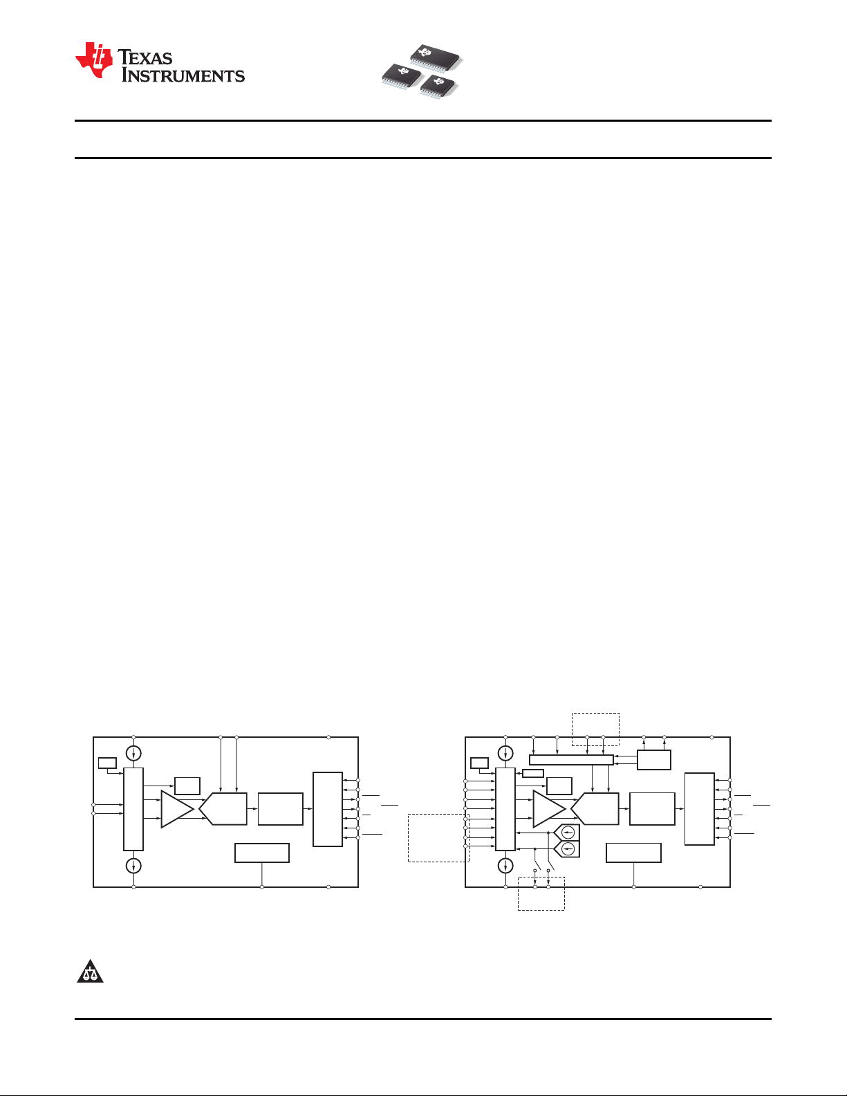
FEATURES DESCRIPTION
23
• 24 Bits, No Missing Codes
• Data Output Rates Up to 2kSPS
• Single-Cycle Settling for All Data Rates
• Simultaneous 50/60Hz Rejection at 20SPS
• 4 Differential/7 Single-Ended Inputs (ADS1248) single-cycle settling digital filter, and an internal
• 2 Differential/3 Single-Ended Inputs (ADS1247)
• Low-Noise PGA: 48nV at PGA = 128
• Matched Current Source DACs
• Very Low Drift Internal Voltage Reference:
10ppm/ ° C (max)
• Sensor Burnout Detection
• 4/8 General-Purpose I/Os (ADS1247/48)
• Internal Temperature Sensor
• Power Supply and V
Monitoring
REF
• Self and System Calibration
• SPI™-Compatible Serial Interface
• Unipolar (+3.3V to +5V)/Bipolar ( ± 2.5V)
Operation
• Digital Supply: +3.3V or +5V
• Operating Temperature – 40 ° C to +125 ° C
APPLICATIONS
• Temperature Measurement
– RTDs, Thermocouples, and Thermistors
• Pressure Measurement
• Industrial Process Control
The ADS1246, ADS1247, and ADS1248 are
highly-integrated, precision, 24-bit analog-to-digital
converters (ADCs). The ADS1246/7/8 feature an
onboard, low-noise, programmable gain amplifier
(PGA), a precision delta-sigma ADC with a
oscillator. The ADS1247 and ADS1248 also provide a
built-in, very low drift voltage reference with 10mA
output capacity, and two matched programmable
current digital-to-analog converters (DACs). The
ADS1246/7/8 provide a complete front-end solution
for temperature/bridge sensor applications including
thermal couples, thermistors, RTDs, and strain-gauge
applications.
An input multiplexer supports four differential inputs
for the ADS1248, two for the ADS1247, and one for
the ADS1246. In addition, the multiplexer has a
sensor burnout detect, voltage bias for
thermocouples, system monitoring, and
general-purpose digital I/Os (ADS1247 and
ADS1248). The onboard, low-noise PGA provides
selectable gains of 1 to 128. The delta-sigma
modulator and programmable digital filter settle in
only one cycle, for fast channel cycling when using
the input multiplexer, and support data rates up to
2kSPS. For data rates of 20SPS or less, both 50Hz
and 60Hz interference are rejected by the filter.
The ADS1246 is offered in a small TSSOP-16
package, the ADS1247 is available in a TSSOP-20
package, and the ADS1248 in a TSSOP-28 package.
All three devices are specified over the extended
temperature range of – 40 ° C to +105 ° C.
ADS1246
ADS1247
ADS1248
1
Please be aware that an important notice concerning availability, standard warranty, and use in critical applications of Texas
Instruments semiconductor products and disclaimers thereto appears at the end of this data sheet.
2 SPI is a trademark of Motorola, Inc.
3 All other trademarks are the property of their respective owners.
PRODUCTION DATA information is current as of publication date.
Products conform to specifications per the terms of the Texas
Instruments standard warranty. Production processing does not
necessarily include testing of all parameters.
Copyright © 2008 – 2009, Texas Instruments Incorporated
ADS1246
ADS1247
ADS1248
SBAS426B – AUGUST 2008 – REVISED MARCH 2009 ....................................................................................................................................................
This integrated circuit can be damaged by ESD. Texas Instruments recommends that all integrated circuits be handled with
appropriate precautions. Failure to observe proper handling and installation procedures can cause damage.
ESD damage can range from subtle performance degradation to complete device failure. Precision integrated circuits may be more
susceptible to damage because very small parametric changes could cause the device not to meet its published specifications.
www.ti.com
PACKAGE/ORDERING INFORMATION
PRODUCT NUMBER OF INPUTS VOLTAGE REFERENCE SOURCES LEAD
ADS1246 or External NO TSSOP-16
ADS1247 or Internal or External YES TSSOP-20
ADS1248 or Internal or External YES TSSOP-28
(1) For the most current package and ordering information, see the Package Option Addendum at the end of this data sheet, or see the TI
website at www.ti.com
ABSOLUTE MAXIMUM RATINGS
1 Differential
1 Single-Ended
2 Differential
3 Single-Ended
4 Differential
7 Single-Ended
(1)
(1)
DUAL SENSOR
EXCITATION CURRENT PACKAGE-
Over operating free-air temperature range (unless otherwise noted).
PARAMETER ADS1246, ADS1247, ADS1248 UNIT
AVDD to AVSS – 0.3 to +5.5 V
AVSS to DGND – 2.8 to +0.3 V
DVDD to DGND – 0.3 to +5.5 V
Input current
Analog input voltage to AVSS AVSS – 0.3 to AVDD + 0.3 V
Digital input voltage to DGND – 0.3 to DVDD + 0.3 V
Maximum junction temperature +150 ° C
Operating temperature range – 40 to +125 ° C
Storage temperature range – 60 to +150 ° C
(1) Stresses beyond those listed under Absolute Maximum Ratings may cause permanent damage to the device. These are stress ratings
only, and functional operation of the device at these or any other conditions beyond those indicated is not implied. Exposure to
absolute-maximum-rated conditions for extended periods may affect device reliability.
100, momentary mA
10, continuous mA
2 Submit Documentation Feedback Copyright © 2008 – 2009, Texas Instruments Incorporated
Product Folder Link(s): ADS1246 ADS1247 ADS1248
(V )(Gain)
IN
2
AVSS 0.1V+ +
AVDD 0.1V- -
(V )(Gain)
IN
2
ADS1246
ADS1247
ADS1248
www.ti.com
ELECTRICAL CHARACTERISTICS
All specifications at TA= – 40 ° C to +105 ° C, AVDD = +5V, DVDD = +3.3V, AVSS = DVSS = 0V, and V
otherwise noted.
ANALOG INPUTS
Full-scale input voltage
(V
IN
Common-mode input range V
Differential input current 100 pA
PGA gain settings 1, 2, 4, 8, 16, 32, 64, 128
Burnout current source 0.5, 2, or 10 µ A
Bias voltage (AVDD + AVSS)/2 V
Bias voltage output impedance 400 Ω
SYSTEM PERFORMANCE
Resolution No missing codes 24 Bits
Data rate 5, 10, 20, 40, 80, 160, 320, 640, 1000, 2000 SPS
Integral nonlinearity (INL) Differential input, best fit, PGA = 1 6 15 ppm
Offset error After calibration – 15 15 µ V
Offset drift see Figure 8 to Figure 11 nV/ ° C
Gain error All PGAs, data rate = 40, 80, or 160SPS – 0.02 ± 0.005 0.02 %
Gain drift PGA = 1 see Figure 12 to Figure 15 ppm/ ° C
ADC conversion time Single-cycle settling
Noise See Table 5 to Table 8
Normal-mode rejection See Table 10
Common-mode rejection
Power-supply rejection AVDD, DVDD at dc 100 135 dB
VOLTAGE REFERENCE INPUT
Voltage reference input
(V
REF
Negative reference input (REFN) AVSS – 0.1 REFP – 0.5 V
Positive reference input (REFP) REFN + 0.5 AVDD + 0.1 V
Reference input current 30 nA
ON-CHIP VOLTAGE REFERENCE
Output voltage 2.038 2.048 2.058 V
Output current
Load regulation 50 µ V/mA
Drift
Startup time See Table 11 µ s
Quiescent current Additional AVDD current 180 µ A
(1) Do not exceed this loading on the internal voltage reference.
(2) Specified by the combination of design and final production test.
.................................................................................................................................................... SBAS426B – AUGUST 2008 – REVISED MARCH 2009
REF
ADS1246, ADS1247, ADS1248
PARAMETER CONDITIONS MIN TYP MAX UNIT
± V
/PGA V
= ADCINP – ADCINN)
(2)
At dc, PGA = 1 80 90 dB
At dc, PGA = 32 90 125 dB
= V
– V
REFP
)
REFN
(1)
TA= +25 ° C to +105 ° C 2 10 ppm/ ° C
TA= – 40 ° C to +105 ° C 6 15 ppm/ ° C
0.5 (AVDD – AVSS) – 1 V
REF
= +2.048V, unless
± 10 mA
Copyright © 2008 – 2009, Texas Instruments Incorporated Submit Documentation Feedback 3
Product Folder Link(s): ADS1246 ADS1247 ADS1248
ADS1246
ADS1247
ADS1248
SBAS426B – AUGUST 2008 – REVISED MARCH 2009 ....................................................................................................................................................
ELECTRICAL CHARACTERISTICS (continued)
All specifications at TA= – 40 ° C to +105 ° C, AVDD = +5V, DVDD = +3.3V, AVSS = DVSS = 0V, and V
otherwise noted.
ADS1246, ADS1247, ADS1248
PARAMETER CONDITIONS MIN TYP MAX UNIT
CURRENT SOURCES (IDACS)
Output current 50, 100, 250, 500, 750, 1000, 1500 µ A
Voltage compliance All currents AVDD – 0.7 V
Initial error All currents, each IDAC – 6 ± 1.0 6 % of FS
Initial mismatch All currents, between IDACs ± 0.03 % of FS
Temperature drift Each IDAC 200 ppm/ ° C
Temperature drift matching Between IDACs 10 ppm/ ° C
SYSTEM MONITORS
Temperature
sensor reading
GENERAL-PURPOSE INPUT/OUTPUT (GPIO)
Logic levels
DIGITAL INPUT/OUTPUT (other than GPIO)
Logic levels
Input leakage DGND < VIN< DVDD ± 10 µ A
Clock input
(CLK)
Internal oscillator frequency 3.89 4.096 4.3 MHz
POWER SUPPLY
DVDD 3.234 5.25 V
AVSS – 2.5 0 V
AVDD AVSS + 3.234 AVSS + 5.25 V
DVDD current Normal mode, DVDD = 3.3V,
AVDD current Converting, AVDD = 3.3V,
Power dissipation
TEMPERATURE RANGE
Specified – 40 +105 ° C
Operating – 40 +125 ° C
Storage – 60 +150 ° C
Voltage TA= +25 ° C 112 mV
Drift 379 µ V/ ° C
V
IH
V
IL
V
OH
V
OL
V
IH
V
IL
V
OH
V
OL
Frequency 1 4.5 MHz
Duty cycle 25 75 %
IOH= 1mA 0.8AVDD V
IOL= 1mA 0.2 AVDD V
IOH= 1mA 0.8DVDD V
IOL= 1mA DGND 0.2 DVDD V
Normal mode, DVDD = 5V,
data rate = 80SPS, internal oscillator
data rate = 20SPS, internal oscillator
Sleep mode 0.2 µ A
Converting, AVDD = 5V,
data rate = 80SPS, internal oscillator
data rate = 20SPS, internal oscillator
Sleep mode 0.1 µ A
AVDD = DVDD = 5V,
data rate = 80SPS, internal oscillator
AVDD = DVDD = 3.3V,
data rate = 20SPS, internal oscillator
0.7AVDD AVDD V
AVSS 0.3AVDD V
0.7DVDD DVDD V
DGND 0.3DVDD V
230 µ A
210 µ A
350 µ A
212 µ A
2.9 mW
1.2 mW
= +2.048V, unless
REF
www.ti.com
4 Submit Documentation Feedback Copyright © 2008 – 2009, Texas Instruments Incorporated
Product Folder Link(s): ADS1246 ADS1247 ADS1248
DVDD
DGND
CLK
RESET
REFP0/GPIO0
REFN0/GPIO1
REFP1
REFN1
VREFOUT
VREFCOM
AIN0/IEXC
AIN1/IEXC
AIN4/IEXC/GPIO4
AIN5/IEXC/GPIO5
SCLK
DIN
DOUT/DRDY
DRDY
CS
START
AVDD
AVSS
IEXC1
IEXC2
AIN3/IEXC/GPIO3
AIN2/IEXC/GPIO2
AIN7/IEXC/GPIO7
AIN6/IEXC/GPIO6
1
2
3
4
5
6
7
8
9
10
11
12
13
14
28
27
26
25
24
23
22
21
20
19
18
17
16
15
ADS1248
ADS1246
ADS1247
ADS1248
www.ti.com
.................................................................................................................................................... SBAS426B – AUGUST 2008 – REVISED MARCH 2009
PIN CONFIGURATIONS
PW PACKAGE
TSSOP-28
(TOP VIEW)
ADS1248 (TSSOP-28) PIN DESCRIPTIONS
NAME PIN NO. INPUT/OUTPUT DESCRIPTION
DVDD 1 Digital Digital Power Supply
DGND 2 Digital Digital Ground
CLK 3 Digital Input External Clock Input. Tie this pin to DGND to activate the internal oscillator.
RESET 4 Digital Input Chip Reset (active low). Returns all register values to reset values.
REFP0/GPIO0 5
REFN0/GPIO1 6
REFP1 7 Analog Input Positive External Reference 1 Input
REFN1 8 Analog Input Negative External Reference 1 Input
VREFOUT 9 Analog Output Positive Internal Reference Voltage Output
VREFCOM 10 Analog Output
AIN0/IEXC 11 Analog Input Analog Input 0, optional Excitation Current Output
AIN1/IEXC 12 Analog Input Analog Input 1, optional Excitation Current Output
AIN4/IEXC/GPIO4 13
AIN5/IEXC/GPIO5 14
AIN6/IEXC/GPIO6 15
AIN7/IEXC/GPIO7 16
AIN2/IEXC/GPIO2 17
Copyright © 2008 – 2009, Texas Instruments Incorporated Submit Documentation Feedback 5
ANALOG/DIGITAL
Analog Input Positive External Reference Input 0, or
Digital In/Out General-Purpose Digital Input/Output Pin 0
Analog Input Negative External Reference 0 Input, or
Digital In/Out General-Purpose Digital Input/Output Pin 1
Negative Internal Reference Voltage Output. Connect this pin to AVSS when using a unipolar
supply, or to the midvoltage of the power supply when using a bipolar supply.
Analog Input Analog Input 4, optional Excitation Current Output, or
Digital In/Out General-Purpose Digital Input/Output Pin 4
Analog Input Analog Input 5, optional Excitation Current Output, or
Digital In/Out General-Purpose Digital Input/Output Pin 5
Analog Input Analog Input 6, optional Excitation Current Output, or
Digital In/Out General-Purpose Digital Input/Output Pin 6
Analog Input Analog Input 7, optional Excitation Current Output, or
Digital In/Out General-Purpose Digital Input/Output Pin 7
Analog Input Analog Input 2, optional Excitation Current Output, or
Digital In/Out General-Purpose Digital Input/Output Pin 2
Product Folder Link(s): ADS1246 ADS1247 ADS1248
ADS1246
ADS1247
ADS1248
SBAS426B – AUGUST 2008 – REVISED MARCH 2009 ....................................................................................................................................................
ADS1248 (TSSOP-28) PIN DESCRIPTIONS (continued)
NAME PIN NO. INPUT/OUTPUT DESCRIPTION
AIN3/IEXC/GPIO3 18
IOUT2 19 Analog Output Excitation Current Output 2
IOUT1 20 Analog Output Excitation Current Output 1
AVSS 21 Analog Negative Analog Power Supply
AVDD 22 Analog Positive Analog Power Supply
START 23 Digital Input Conversion start. See text for complete description.
CS 24 Digital Input Chip Select (active low)
DRDY 25 Digital Output Data Ready (active low)
DOUT/ DRDY 26 Digital Output
DIN 27 Digital Input Serial Data Input
SCLK 28 Digital Input Serial Clock Input
ANALOG/DIGITAL
Analog Input Analog Input 3, optional Excitation Current Output, or
Digital In/Out General-Purpose Digital Input/Output Pin 3
Serial Data Out Output, or
Data Out combined with Data Ready (active low when DRDY function enabled)
www.ti.com
6 Submit Documentation Feedback Copyright © 2008 – 2009, Texas Instruments Incorporated
Product Folder Link(s): ADS1246 ADS1247 ADS1248
DVDD
DGND
CLK
RESET
REFP0/GPIO0
REFN0/GPIO1
VREFOUT
VREFCOM
AIN0/IEXC
AIN1/IEXC
SCLK
DIN
DOUT/DRDY
DRDY
CS
START
AVDD
AVSS
AIN3/IEXC/GPIO3
AIN2/IEXC/GPIO2
1
2
3
4
5
6
7
8
9
10
20
19
18
17
16
15
14
13
12
11
ADS1247
ADS1246
ADS1247
ADS1248
www.ti.com
DVDD 1 Digital Digital Power Supply
DGND 2 Digital Digital Ground
CLK 3 Digital Input External Clock Input. Tie this pin to DGND to activate the internal oscillator.
RESET 4 Digital Input Chip Reset (active low). Returns all register values to reset values.
REFP0/GPIO0 5
REFN0/GPIO1 6
VREFOUT 7 Analog Output Positive Internal Reference Voltage Output
VREFCOM 8 Analog Output
AIN0/IEXC 9 Analog Input Analog Input 0, optional Excitation Current Output
AIN1/IEXC 10 Analog Input Analog Input 1, optional Excitation Current Output
AIN2/IEXC/GPIO2 11
AIN3/IEXC/GPIO3 12
AVSS 13 Analog Negative Analog Power Supply
AVDD 14 Analog Positive Analog Power Supply
START 15 Digital Input Conversion Start. See text for description of use.
CS 16 Digital Input Chip Select (active low)
DRDY 17 Digital Output Data Ready (active low)
DOUT/ DRDY 18 Digital Output
DIN 19 Digital Input Serial Data Input
SCLK 20 Digital Input Serial Clock Input
Copyright © 2008 – 2009, Texas Instruments Incorporated Submit Documentation Feedback 7
.................................................................................................................................................... SBAS426B – AUGUST 2008 – REVISED MARCH 2009
PW PACKAGE
TSSOP-20
(TOP VIEW)
ADS1247 (TSSOP-20) PIN DESCRIPTIONS
NAME PIN NO. INPUT/OUTPUT DESCRIPTION
ANALOG/DIGITAL
Analog Input Positive External Reference Input, or
Digital In/Out General-Purpose Digital Input/Output Pin 0
Analog Input Negative External Reference Input, or
Digital In/Out General-Purpose Digital Input/Output Pin 1
Analog Input Analog Input 2, optional Excitation Current Output, or
Digital In/Out General-Purpose Digital Input/Output Pin 2
Analog Input Analog Input 3, with or without Excitation Current Output, or
Digital In/Out General-Purpose Digital Input/Output Pin 3
Product Folder Link(s): ADS1246 ADS1247 ADS1248
Negative Internal Reference Voltage Output. Connect this pin to AVSS when using a unipolar
supply, or to the midvoltage of the power supply when using a bipolar supply.
Serial Data Out Output, or
Data Out combined with Data Ready (active low when DRDY function enabled)
DVDD
DGND
CLK
RESET
REFP
REFN
AINP
AINN
SCLK
DIN
DOUT/DRDY
DRDY
CS
START
AVDD
AVSS
1
2
3
4
5
6
7
8
16
15
14
13
12
11
10
9
ADS1246
ADS1246
ADS1247
ADS1248
SBAS426B – AUGUST 2008 – REVISED MARCH 2009 ....................................................................................................................................................
PW PACKAGE
TSSOP-16
(TOP VIEW)
ADS1246 (TSSOP-16) PIN DESCRIPTIONS
NAME PIN NO. INPUT/OUTPUT DESCRIPTION
DVDD 1 Digital Digital Power Supply
DGND 2 Digital Digital Ground
CLK 3 Digital Input External Clock Input. Tie this pin to DGND to activate the internal oscillator.
RESET 4 Digital Input Chip Reset (active low). Returns all register values to reset values.
REFP 5 Analog Input Positive External Reference Input
REFN 6 Analog Input Negative External Reference Input
AINP 7 Analog Input Positive Analog Input
AINN 8 Analog Input Negative Analog Input
AVSS 9 Analog Negative Analog Power Supply
AVDD 10 Analog Positive Analog Power Supply
START 11 Digital Input Conversion Start. See text for description of use.
CS 12 Digital Input Chip Select (active low)
DRDY 13 Digital Output Data Ready (active low)
DOUT/ DRDY 14 Digital Output
DIN 15 Digital Input Serial Data Input
SCLK 16 Digital Input Serial Clock Input
ANALOG/DIGITAL
Serial Data Out Output, or
Data Out combined with Data Ready (active low when DRDY function enabled)
www.ti.com
8 Submit Documentation Feedback Copyright © 2008 – 2009, Texas Instruments Incorporated
Product Folder Link(s): ADS1246 ADS1247 ADS1248
SCLK
DOUT[7] DOUT[6] DOUT[5] DOUT[4] DOUT[1] DOUT[0]
DIN[0] DIN[7] DIN[6] DIN[5] DIN[4] DIN[1] DIN[0]
CS
DOUT/DRDY
(1)
DIN
t
CSSC
t
DIST
t
DIHD
t
SCLK
t
SCCS
t
CSDO
t
DOPD
t
SPWL
t
SPWH
t
DOHD
SCLK
(3)
1 2 3 87654
DRDY
t
STD
t
DTS
t
PWH
ADS1246
ADS1247
ADS1248
www.ti.com
TIMING DIAGRAMS
.................................................................................................................................................... SBAS426B – AUGUST 2008 – REVISED MARCH 2009
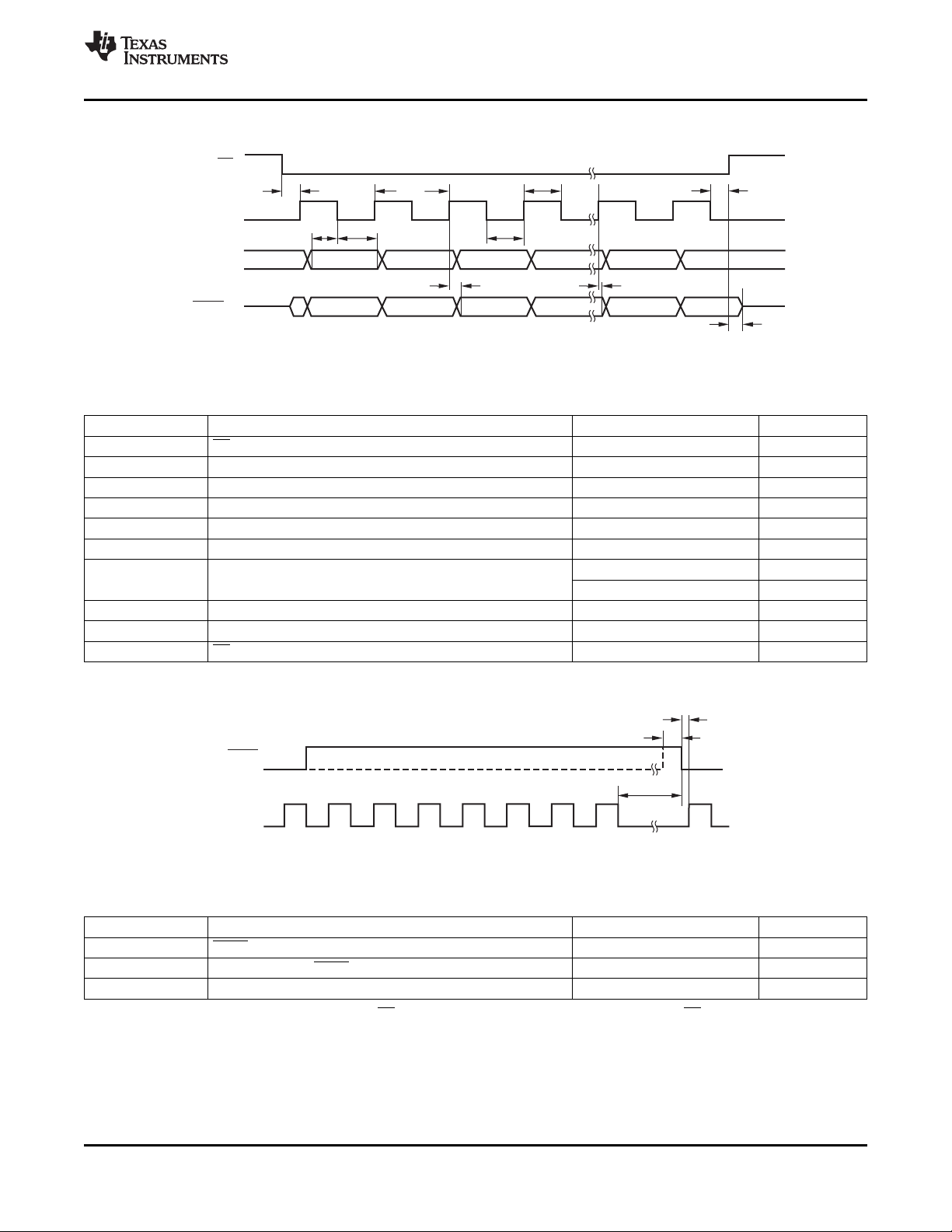
Figure 1. Serial Interface Timing
Table 1. Timing Characteristics for Figure 1
(1)
SYMBOL DESCRIPTION MIN MAX UNIT
t
CSSC
t
SCCS
t
DIST
t
DIHD
t
DOPD
t
DOHD
t
SCLK
t
SPWH
t
SPWL
t
CSDO
CS low to first SCLK high (set up time) 10 ns
SCLK low to CS high (hold time) 7 t
DIN set up time 5 ns
DIN hold time 5 ns
SCLK rising edge to new data valid 30 ns
DOUT hold time 0 ns
SCLK period
500 ns
SCLK pulse width high 0.25 0.75 t
SCLK pulse width low 0.25 0.75 t
CS high to DOUT high impedance 10 ns
(1) DRDY MODE bit = 0.
(2) t
= 1/f
OSC
. The default clock frequency f
CLK
= 4.096MHz. Expect a ± 5% variation whan the internal oscillator is used.
CLK
(2)
OSC
64 conversions
SCLK
SCLK
Figure 2. SPI Interface Timing to Allow Conversion Result Loading
(3) (4)
Table 2. Timing Characteristics for Figure 2
SYMBOL DESCRIPTION MIN MAX UNIT
t
PWH
t
STD
t
DTS
(3) This timing diagram is applicable only when the CS pin is low. SCLK need not be low during t
(4) SCLK should only be sent in multiples of eight during partial retrieval of output data.
Copyright © 2008 – 2009, Texas Instruments Incorporated Submit Documentation Feedback 9
DRDY pulse width high 3 t
SCLK low prior to DRDY low 5 t
DRDY falling edge to SCLK rising edge 30 ns
when CS is high.
STD
Product Folder Link(s): ADS1246 ADS1247 ADS1248
OSC
OSC
t
START
START
SCLK
CS
RESET
t
RESET
t
RHSC
ADS1246
ADS1247
ADS1248
SBAS426B – AUGUST 2008 – REVISED MARCH 2009 ....................................................................................................................................................
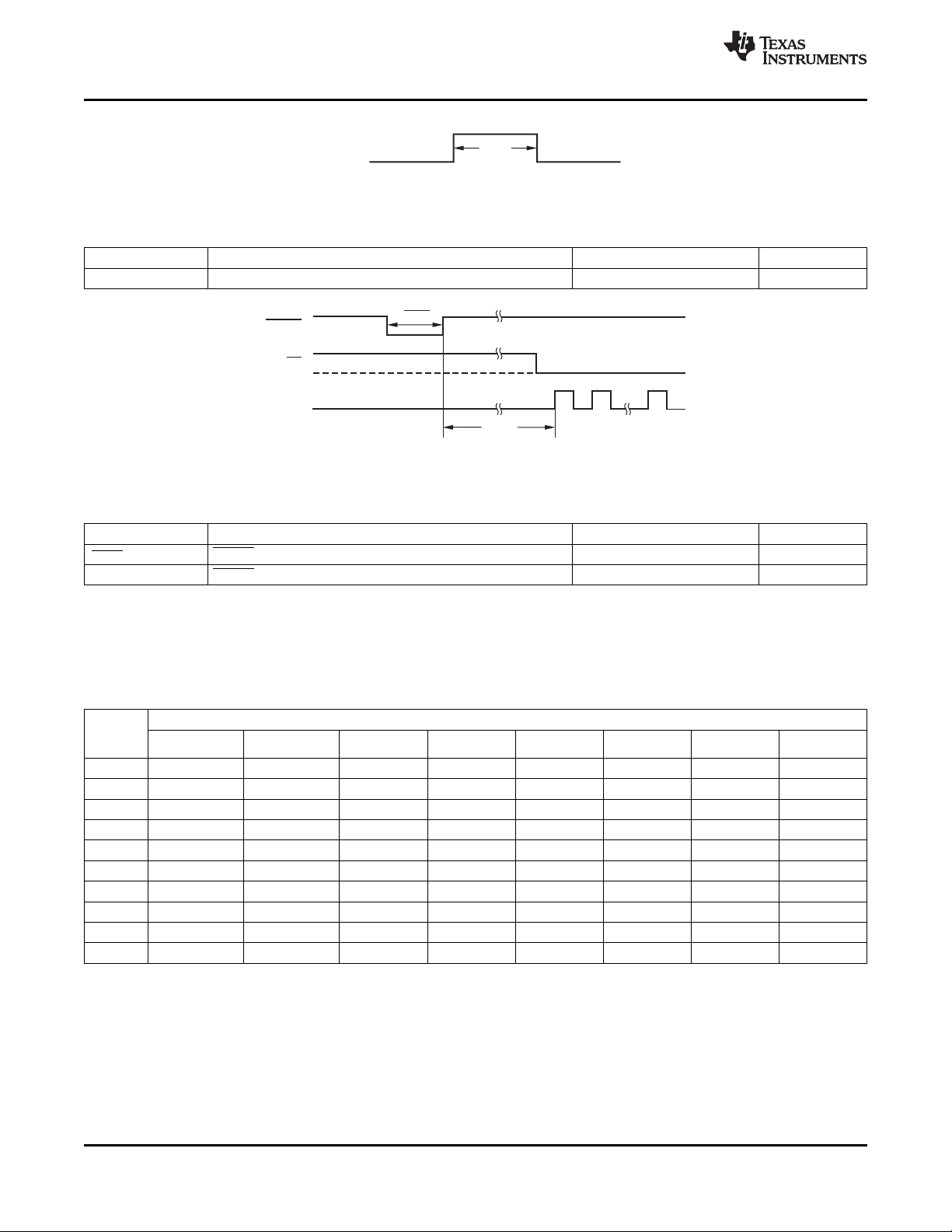
Figure 3. Minimum START Pulse Width
Table 3. Timing Characteristics for Figure 3
SYMBOL DESCRIPTION MIN MAX UNIT
t
START
START pulse width high 3 t
Figure 4. Reset Pulse Width and SPI Communication After Reset
www.ti.com
OSC
Table 4. Timing Characteristics for Figure 4
SYMBOL DESCRIPTION MIN MAX UNIT
t
RESET
t
RHSC
(1) Applicable only when f
RESET pulse width low 4 t
RESET high to SPI communication start 0.6
= 4.096MHz and scales proportionately with f
OSC
frequency.
OSC
(1)
NOISE PERFORMANCE
Table 5. Noise in µ V, rms and ( µ V, peak-to-peak) at AVDD = DVDD = 5V, AVSS = DGND = 0V,
Using Internal Reference (2.048V)
DATA PGA SETTING
RATE
(SPS) 1 2 4 8 16 32 64 128
5 1.79 (8.10) 0.76 (3.90) 0.40 (2.00) 0.23 (1.05) 0.12 (0.63) 0.08 (0.39) 0.07 (0.34) 0.06 (0.32)
10 2.46 (13.80) 1.04 (5.50) 0.56 (2.75) 0.31 (1.75) 0.14 (0.78) 0.10 (0.46) 0.09 (0.52) 0.08 (0.43)
20 3.20 (14.00) 1.53 (8.00) 0.85 (5.00) 0.45 (2.80) 0.25 (1.17) 0.16 (0.73) 0.12 (0.56) 0.11 (0.63)
40 3.30 (18.00) 1.50 (7.80) 0.86 (4.84) 0.40 (2.16) 0.30 (1.75) 0.20 (1.25) 0.17 (0.87) 0.16 (0.85)
80 4.60 (27.10) 2.23 (14.00) 1.00 (4.80) 0.64 (3.25) 0.38 (2.40) 0.29 (1.82) 0.27 (1.69) 0.23 (1.30)
160 7.00 (42.00) 3.30 (20.00) 1.52 (9.25) 0.83 (5.10) 0.55 (3.14) 0.41 (3.00) 0.35 (2.14) 0.34 (2.40)
320 10.60 (67.00) 5.60 (40.00) 2.90 (17.50) 1.47 (8.70) 0.85 (5.14) 0.59 (4.03) 0.49 (3.10) 0.48 (3.10)
640 15.80 (101.00) 8.30 (52.00) 4.20 (24.80) 2.14 (15.50) 1.23 (8.25) 0.82 (5.21) 0.67 (4.55) 0.66 (4.30)
1000 38.00 (420.00) 19.70 (190.00) 8.80 (67.50) 4.50 (40.30) 2.64 (24.80) 1.47 (14.34) 0.96 (6.23) 0.83 (5.30)
2000 40.80 (449.00) 18.40 (179.00) 9.30 (87.00) 4.80 (43.50) 2.56 (22.60) 1.63 (11.90) 1.32 (10.60) 1.23 (7.40)
OSC
ms
10 Submit Documentation Feedback Copyright © 2008 – 2009, Texas Instruments Incorporated
Product Folder Link(s): ADS1246 ADS1247 ADS1248

EffectiveNumberofBits=
ln(FSR/Noise)
ln(2)
EffectiveNumberofBits=
ln(FSR/Noise)
ln(2)
www.ti.com
.................................................................................................................................................... SBAS426B – AUGUST 2008 – REVISED MARCH 2009
Table 6. Effective Number of Bits, rms and (peak-to-peak) Noise Using the Internal Reference (+2.048V)
DATA PGA SETTING
RATE
(SPS) 1 2 4 8 16 32 64 128
5 21.50 (19.10) 21.60 (19.30) 21.60 (19.20) 21.40 (19.20) 21.30 (19.00) 20.90 (18.60) 20.10 (17.80) 19.20 (17.00)
10 21.00 (18.50) 21.20 (18.80) 21.10 (18.80) 21.00 (18.40) 20.90 (18.40) 20.50 (18.10) 19.70 (17.40) 18.70 (16.60)
20 20.60 (18.40) 20.60 (18.20) 20.50 (17.90) 20.40 (17.80) 20.30 (17.80) 20.00 (17.50) 19.20 (16.60) 18.20 (16.00)
40 20.50 (18.10) 20.70 (18.30) 20.50 (18.00) 20.60 (18.10) 20.10 (17.90) 19.60 (17.30) 18.90 (16.50) 17.80 (15.40)
80 20.10 (17.50) 20.10 (17.40) 20.30 (18.00) 19.90 (17.60) 19.70 (17.40) 19.20 (16.40) 18.30 (16.00) 17.40 (15.20)
160 19.40 (16.90) 19.60 (17.00) 19.60 (17.10) 19.50 (16.90) 19.40 (16.60) 18.70 (16.30) 17.80 (15.20) 16.80 (14.50)
320 18.90 (16.20) 18.80 (16.00) 18.70 (16.10) 18.70 (16.20) 18.50 (16.10) 18.00 (15.60) 17.30 (14.80) 16.40 (13.80)
640 18.30 (15.60) 18.20 (15.60) 18.20 (17.50) 18.20 (15.30) 18.00 (15.30) 17.60 (15.20) 16.70 (14.10) 15.90 (13.20)
1000 17.00 (13.50) 16.90 (13.70) 17.10 (14.20) 17.10 (13.90) 16.90 (13.80) 16.80 (13.50) 16.30 (13.60) 15.50 (12.70)
2000 16.90 (13.40) 17.10 (13.80) 17.00 (13.80) 17.00 (13.80) 16.80 (13.40) 16.50 (13.70) 15.90 (13.20) 14.90 (12.20)
(1)
Table 7. Noise in µ V, rms and ( µ V, peak-to-peak) at AVDD = DVDD = 5V, AVSS = DGND = 0V,
Using External Reference (2.5V)
DATA PGA SETTING
RATE
(SPS) 1 2 4 8 16 32 64 128
5 1.22 (5.50) 0.75 (4.20) 0.41 (2.10) 0.21 (1.10) 0.11 (0.48) 0.07 (0.34) 0.06 (0.3) 0.05 (0.23)
10 1.67 (9.83) 0.89 (4.02) 0.55 (2.98) 0.30 (1.07) 0.16 (0.73) 0.09 (0.54) 0.07 (0.39) 0.07 (0.37)
20 2.55 (14.90) 1.33 (7.45) 0.77 (4.25) 0.37 (2.09) 0.20 (1.10) 0.13 (0.77) 0.11 (0.57) 0.10 (0.59)
40 3.03 (19.07) 1.46 (8.49) 0.75 (4.25) 0.41 (2.46) 0.24 (1.27) 0.15 (0.84) 0.16 (0.86) 0.15 (0.83)
80 3.95 (24.73) 2.04 (13.56) 0.88 (5.74) 0.54 (3.80) 0.33 (2.16) 0.21 (1.35) 0.21 (1.28) 0.19 (1.18)
160 5.71 (45.59) 2.80 (19.52) 1.43 (10.06) 0.74 (5.70) 0.45 (3.20) 0.29 (2.11) 0.29 (1.90) 0.28 (1.89)
320 10.41 (82.84) 5.18 (43.06) 2.97 (21.15) 1.35 (10.91) 0.76 (5.70) 0.50 (3.39) 0.41 (3.02) 0.39 (2.67)
640 14.58 (130.50) 7.52 (64.21) 4.01 (31.71) 1.68 (11.74) 1.05 (9.58) 0.70 (5.39) 0.58 (4.07) 0.54 (3.92)
1000 35.52 (481.70) 17.64 (206.40) 12.77 (102.00) 5.11 (41.60) 2.21 (25.67) 1.26 (13.53) 0.84 (8.03) 0.71 (5.48)
2000 35.42 (415.20) 17.41 (199.60) 8.76 (101.00) 4.51 (50.54) 2.43 (26.18) 1.51 (13.60) 1.18 (8.78) 1.08 (7.52)
ADS1246
ADS1247
ADS1248
(1)
Table 8. Effective Number of Bits, rms and (peak-to-peak) Noise Using External Reference (+2.5V)
DATA PGA SETTING
RATE
(SPS) 1 2 4 8 16 32 64 128
10 21.50 (19.00) 21.40 (19.20) 21.10 (18.70) 21.00 (18.30) 20.90 (18.70) 20.80 (18.10) 20.10 (17.60) 19.00 (16.70)
20 20.90 (18.40) 20.80 (18.40) 20.60 (18.20) 20.70 (18.20) 20.60 (18.10) 20.20 (17.60) 19.50 (17.10) 18.60 (16.00)
40 20.70 (18.00) 20.70 (18.20) 20.70 (18.20) 20.50 (18.00) 20.30 (17.90) 20.00 (17.50) 18.90 (16.50) 18.00 (15.50)
80 20.30 (17.60) 20.20 (17.50) 20.40 (17.70) 20.10 (17.30) 19.90 (17.10) 19.50 (16.80) 18.50 (15.90) 17.60 (15.00)
160 19.70 (16.70) 19.80 (17.00) 19.70 (16.90) 19.70 (16.70) 19.40 (16.60) 19.10 (16.20) 18.00 (15.30) 17.00 (14.30)
320 18.90 (15.90) 18.90 (15.80) 18.70 (15.90) 18.80 (15.80) 18.70 (15.70) 18.30 (15.50) 17.50 (14.70) 16.60 (13.80)
640 18.40 (15.20) 18.30 (15.20) 18.30 (15.30) 18.50 (15.70) 18.20 (15.00) 17.80 (14.80) 17.00 (14.20) 16.10 (13.30)
1000 17.10 (13.30) 17.10 (13.60) 16.60 (13.60) 16.90 (13.90) 17.10 (13.60) 16.90 (13.50) 16.50 (13.20) 15.80 (12.80)
2000 17.10 (13.60) 17.10 (13.60) 17.10 (13.60) 17.10 (13.60) 17.00 (13.50) 16.70 (13.50) 16.00 (13.10) 15.10 (12.30)
(1)
Copyright © 2008 – 2009, Texas Instruments Incorporated Submit Documentation Feedback 11
5 22.00 (19.80) 21.70 (19.20) 21.60 (19.20) 21.50 (19.20) 21.40 (19.30) 21.00 (18.80) 20.30 (18.00) 19.60 (17.40)
Product Folder Link(s): ADS1246 ADS1247 ADS1248
(1)
Counts
-53
-49
-
45
-41
-37
-33
-29
-26
-
22
-18
-14
-10
-6
-3
0
4
8
12
16
19
23
27
31
35
39
43
47
1800
1600
1400
1200
1000
800
600
400
200
0
PGA=1
DataRate=20SPS
12kSamples
=13s
(LSB)
Counts
-69
-63
-58
-52
-
47
-41
-36
-30
-25
-20
-14
-9
-3
1
7
12
18
23
28
34
39
45
50
56
61
67
73
1800
1600
1400
1200
1000
800
600
400
200
0
PGA=32
DataRate=20SPS
12kSamples
=19s
(LSB)
1.8
1.6
1.4
1.2
1.0
0.8
0.6
RMSNoise(
V)m
V (%ofFSR)
IN
-100 -80 -60 -40 -20 10020 40 60 80
PGA=32
DataRate=5SPS
4
3
2
1
0
-1
-2
-3
Temperature( C)°
Input-ReferredOffset( V)m
-40 -20 0 20 40 60 80 100 120
PGA=32
PGA=1
PGA=128
DataRate=20SPS
8
6
4
2
0
-2
-4
-6
-8
Temperature( C)°
Input-ReferredOffset( V)m
-40 -20 0 20 40 60 80 100 120
PGA=32
PGA=1
PGA=128
DataRate=160SPS
8
6
4
2
0
-2
-4
-6
-8
-10
-12
-14
Temperature( C)°
Input-ReferredOffset( V)m
-40 -20 0 20 40 60 80 100 120
PGA=32
PGA=1
PGA=128
DataRate=640SPS
ADS1246
ADS1247
ADS1248
SBAS426B – AUGUST 2008 – REVISED MARCH 2009 ....................................................................................................................................................
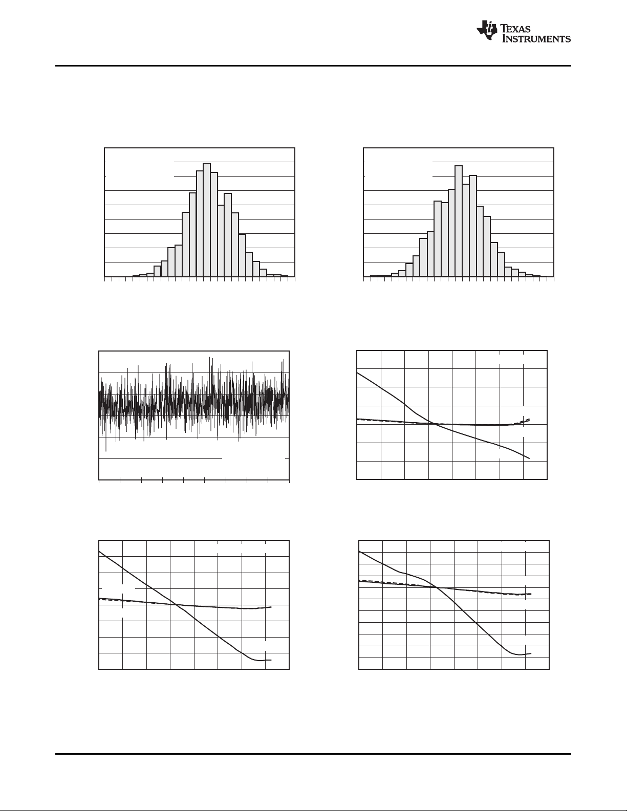
TYPICAL CHARACTERISTICS
At TA= +25 ° C, AVDD = DVDD = 5V, V
NOISE HISTOGRAM PLOT NOISE HISTOGRAM PLOT
Figure 5. Figure 6.
= 2.5V, and AVSS = DVSS = 0V, unless otherwise noted.
REF
www.ti.com
RMS NOISE
vs INPUT SIGNAL OFFSET vs TEMPERATURE
Figure 7. Figure 8.
OFFSET vs TEMPERATURE OFFSET vs TEMPERATURE
12 Submit Documentation Feedback Copyright © 2008 – 2009, Texas Instruments Incorporated
Figure 9. Figure 10.
Product Folder Link(s): ADS1246 ADS1247 ADS1248
15
10
5
0
-5
-10
-15
Temperature(°C)
Input-ReferredOffset(
m
V)
-40 -20 0 20 40 60 80 100 120
PGA=32
DataRate=2kSPS
PGA=1
PGA=128
0.05
0.04
0.03
0.02
0.01
0
-0.01
-0.02
-0.03
-0.04
-0.05
Temperature( C)°
GainError(%)
-40 -20 0 20 40 60 80 100 120
PGA=32
PGA=1
PGA=128
DataRate=20SPS
0.03
0.02
0.01
0
-0.01
-0.02
-0.03
-0.04
Temperature( C)°
GainError(%)
-40 -20 0 20 40 60 80 100 120
PGA=32
PGA=1
PGA=128
DataRate=160SPS
0.03
0.02
0.01
0
-0.01
-0.02
-0.03
-0.04
Temperature( C)°
GainError(%)
-40 -20 0 20 40 60 80 100 120
PGA=32
PGA=1
PGA=128
DataRate=640SPS
0.02
0.01
0
-0.01
-0.02
-0.03
-0.04
Temperature( C)°
GainError(%)
-40 -20 0 20 40 60 80 100 120
PGA=32
PGA=1
PGA=128
600
550
500
450
400
350
300
250
200
150
100
DataRate(SPS)
AnalogCurrent( A)m
5 10 20 40 80 160 320 640 1000 2000
AVDD=5V
AVDD=3.3V
www.ti.com
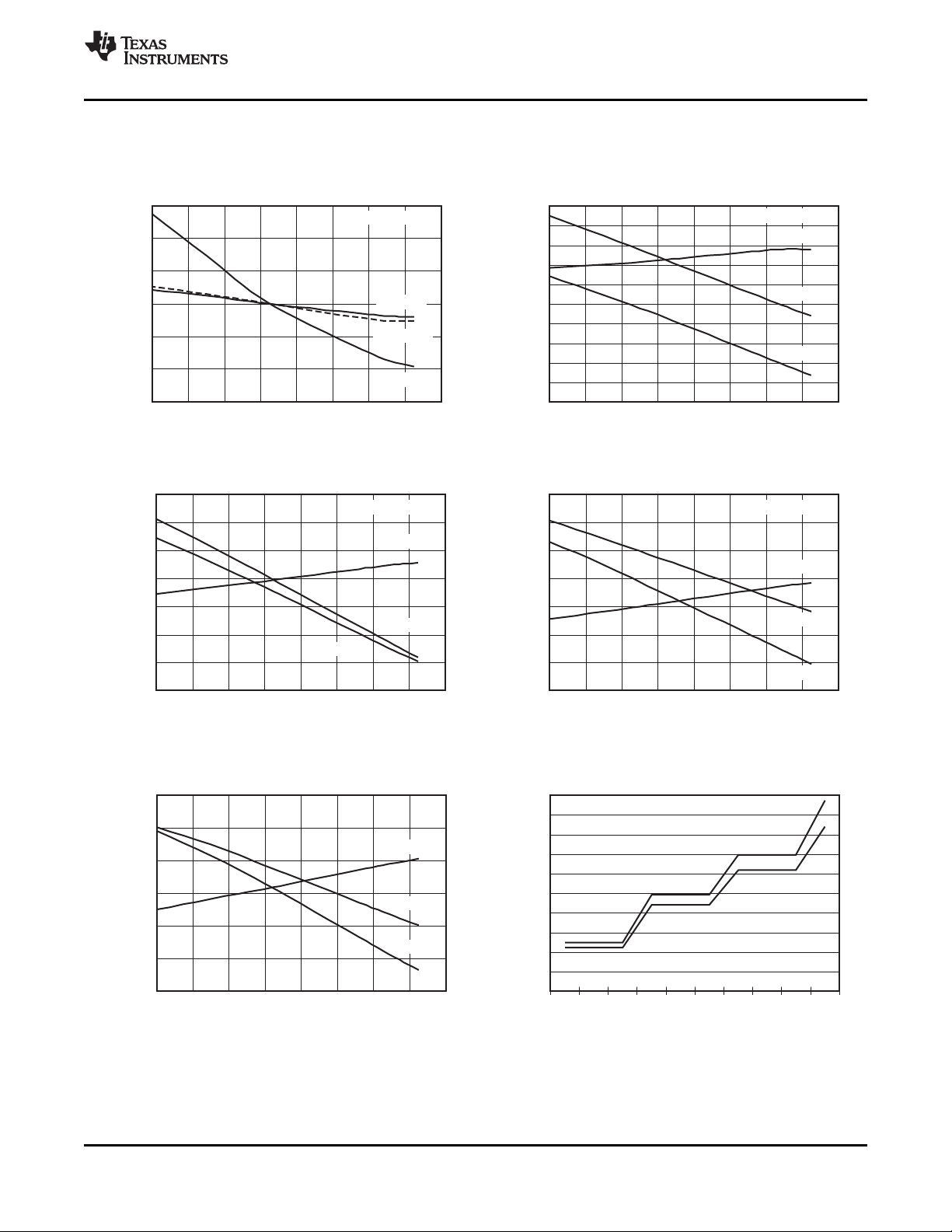
.................................................................................................................................................... SBAS426B – AUGUST 2008 – REVISED MARCH 2009
At TA= +25 ° C, AVDD = DVDD = 5V, V
OFFSET vs TEMPERATURE GAIN vs TEMPERATURE
Figure 11. Figure 12.
GAIN vs TEMPERATURE GAIN vs TEMPERATURE
TYPICAL CHARACTERISTICS (continued)
= 2.5V, and AVSS = DVSS = 0V, unless otherwise noted.
REF
ADS1246
ADS1247
ADS1248
Figure 13. Figure 14.
GAIN vs TEMPERATURE vs DATA RATE
Copyright © 2008 – 2009, Texas Instruments Incorporated Submit Documentation Feedback 13
Figure 15. Figure 16.
ANALOG CURRENT
Product Folder Link(s): ADS1246 ADS1247 ADS1248
290
270
250
230
210
190
170
DataRate(SPS)
DigitalCurrent( A)m
5 10 20 40 80 160 320 640 1000 2000
DVDD=3.3V
DVDD=5V
800
700
600
500
400
300
200
100
0
Temperature( C)°
AnalogCurrent( A)
m
-40 -20 0 20 40 60 80 100 120
5SPS
40SPS
320SPS
2kSPS
330
310
290
270
250
230
210
190
Temperature( C)°
DigitalCurrent( A)m
-40 -20 0 20 40 60 80 100 120
5/10/20SPS
40/80/160SPS
320/640/1kSPS
2kSPS
8
6
4
2
0
-2
-4
-6
-8
V (%ofFSR)
IN
INL(ppmofFSR)
-100 -50 0 50 100
PGA=1
DataRate=20SPS
- °40 C
- °10 C
+25 C°
+105 C°
8
6
4
2
0
-2
-4
-6
-8
-10
V (%ofFSR)
IN
INL(ppmofFSR)
-100 -50 0 50 100
PGA=32
DataRate=20SPS
- °40 C
+25 C°
+105 C°
- °10 C
8
6
4
2
0
-2
-4
-6
-8
V (%ofFSR)
IN
INL(ppmofFSR)
-100 -50 0 50 100
PGA=128
DataRate=20SPS
-40°C
+25 C°
+105 C°
-10°C
ADS1246
ADS1247
ADS1248
SBAS426B – AUGUST 2008 – REVISED MARCH 2009 ....................................................................................................................................................
At TA= +25 ° C, AVDD = DVDD = 5V, V
DIGITAL CURRENT ANALOG CURRENT
vs DATA RATE vs TEMPERATURE
Figure 17. Figure 18.
TYPICAL CHARACTERISTICS (continued)
= 2.5V, and AVSS = DVSS = 0V, unless otherwise noted.
REF
www.ti.com
DIGITAL CURRENT INTEGRAL NONLINEARITY
vs TEMPERATURE vs INPUT SIGNAL
Figure 19. Figure 20.
INTEGRAL NONLINEARITY INTEGRAL NONLINEARITY
vs INPUT SIGNAL vs INPUT SIGNAL
14 Submit Documentation Feedback Copyright © 2008 – 2009, Texas Instruments Incorporated
Figure 21. Figure 22.
Product Folder Link(s): ADS1246 ADS1247 ADS1248
8
6
4
2
0
-2
-4
-6
-8
V (%ofFSR)
IN
INL(ppmofFSR)
-100 -50 0 50 100
PGA=1
DataRate=2kSPS
- °40 C
+25 C°
+105 C°
- °10 C
650
648
646
644
642
640
638
636
634
632
630
Temperature( C)°
DataRate(SPS)
-40 -20 0 20 40 60 80 100 120
DataRate=640SPSusingInternalOscillator
130
125
120
115
110
105
100
95
90
85
80
Temperature( C)°
CMRR(dB)
-40 -20 0 20 40 60 80 100 120
PGA=1
PGA=32
PGA=128
2.050
2.049
2.048
2.047
2.046
Temperature( C)°
OutputVoltage(V)
-40 -20 0 20 40 60 80 100 120
14Units
1.002
1.001
1.000
0.999
0.998
0.997
0.996
0.995
0.994
0.993
0.992
0.991
AVDD(V)
NormalizedOutputCurrent
2.0 2.5 3.0 3.5 4.0 4.5 5.0 5.5 6.0
750 Am
250 Am
1.5mA
500 Am
100 Am
1mA
50 Am
IDACCurrentSettings
0.004
0.003
0.002
0.001
0
-0.001
-0.002
-0.003
-0.004
Temperature( C)°
IEXC1 IEXC2(- mA)
-40 -20 0 20 40 60 80 100 120
1.5mASetting,10Units
www.ti.com
.................................................................................................................................................... SBAS426B – AUGUST 2008 – REVISED MARCH 2009
At TA= +25 ° C, AVDD = DVDD = 5V, V
INTEGRAL NONLINEARITY DATA RATE
vs INPUT SIGNAL vs TEMPERATURE
Figure 23. Figure 24.
TYPICAL CHARACTERISTICS (continued)
= 2.5V, and AVSS = DVSS = 0V, unless otherwise noted.
REF
ADS1246
ADS1247
ADS1248
CMRR INTERNAL V
vs TEMPERATURE vs TEMPERATURE
Figure 25. Figure 26.
IDAC LINE REGULATION IDAC DRIFT
REF
Copyright © 2008 – 2009, Texas Instruments Incorporated Submit Documentation Feedback 15
Figure 27. Figure 28.
Product Folder Link(s): ADS1246 ADS1247 ADS1248

ADS1246
ADS1247
ADS1248
SBAS426B – AUGUST 2008 – REVISED MARCH 2009 ....................................................................................................................................................
GENERAL DESCRIPTION
OVERVIEW
The ADS1246/47/48 are highly integrated, low-noise,
24-bit, delta-sigma ADCs. They include a flexible
input multiplexer, a low-noise, high input impedance
PGA, a built-in very low drift voltage reference with
10mA output capability (ADS1247/48), an internal Any analog input pin can be selected as the positive
temperature sensor, and two highly-matched current input or negative input through the MUX0 register.
sources. An SPI-compatible serial communication The ADS1246/47/48 have a true fully differential
interface is also provided. A set of simple commands mode, meaning that the input signal range can be
control the ADS1246/47/48 devices. from – 2.5V to +2.5V (when AVDD = 2.5V and AVSS
The ADS1246/47/48 provide two conversion modes:
single-conversion and continuous-conversion. In Through the input multiplexer, the ambient
single-conversion mode, the ADC converts the input temperature (internal temperature sensor), AVDD,
signal once and the conversion result (data) is stored DVDD, and external reference can all be selected for
in the data register. The data can be read any time measurement. Refer to the System Monitor section
before the next conversion. Single-conversion mode for details.
can be started by applying a pulse to the START pin
or by executing an SPI command. Upon completing
the conversion, the device goes into sleep mode to
minimize power consumption.
The ADS1246/47/48 also provide a system monitor
function that monitors the external voltage references,
analog power-supply voltage, digital power supply,
and onboard temperature. The burnout current
source can be used to detect sensor open-circuit
conditions.
The ADS1246/47/48 simultaneously reject 50Hz and GPIOs.
60Hz interference with greater than 100dB rejection
ratio for data rates up to 20SPS.
ADC INPUT AND MULTIPLEXER
The ADS1246/47/48 ADC measures the input signal
through the onboard PGA. All analog inputs are
connected to the internal AIN
through the analog multiplexer. A block diagram of
the analog input multiplexer is shown in Figure 29 .
The input multiplexer connects to eight (ADS1248),
four (ADS1247), or two (ADS1246) analog inputs that
or AIN
P
analog inputs
N
can be configured as single-ended inputs, differential
inputs, or in a combination of single-ended and
differential inputs. The multiplexer also allows the
on-chip excitation current and/or bias voltage to be
selected to a specific channel.
= – 2.5V).
On the ADS1247 and ADS1248, the analog inputs
can also be configured as general-purpose
inputs/outputs (GPIOs). See the General-Purpose
Digital I/O section for more details.
ESD diodes protect the ADC inputs. To prevent these
diodes from turning on, make sure the voltages on
the input pins do not go below AVSS by more than
100mV, and do not exceed AVDD by more than
100mV, as shown in Equation 1 . Note that the same
caution is true if the inputs are configured to be
AVSS – 100mV < (AINX) < AVDD + 100mV (1)
Settling Time for Channel Multiplexing
The ADS1246/47/48 is a true single-cycle settling,
delta-sigma converter. After the internal multiplexer
switches, the very first data are valid.
www.ti.com
16 Submit Documentation Feedback Copyright © 2008 – 2009, Texas Instruments Incorporated
Product Folder Link(s): ADS1246 ADS1247 ADS1248
(MUXCAL=001)
SystemMonitors
Temperature
Diode
VREFP
VREFN
VREFP1/4
VREFN1/4
VREFP0/4
VREFN0/4
AVDD/4
AVSS/4
DVDD/4
DVSS/4
ADS1248Only
ADS1247/48Only
VBIAS
AIN0
AIN1
VBIAS
AIN2
VBIAS
AIN3
VBIAS
AIN4
VBIAS
AIN5
VBIAS
AIN6
VBIAS
AIN7
AVDD
IDAC1
IDAC2
AVDD
VBIAS
PGA
AIN
P
AVSS
AVDD
BurnoutCurrentSource
(0.5 A,2 A,10m m mA)
BurnoutCurrentSource
(0.5 A,2 A,10m m mA)
AIN
N
To
ADC
AVSS
AVSS
AVSS
AVSS
AVSS
AVSS
AVSS
AVSS
AVDD
AVDD
AVDD
AVDD
AVDD
AVDD
AVDD
AVDD
AVDD AVDD
REFN1REFP1
ADC
ADS1248 Only
REFN0REFP0
REFNREFP
VREFCOMVREFOUT
ReferenceMultiplexer
Internal
Voltage
Reference
ADS1246
ADS1247
ADS1248
www.ti.com
.................................................................................................................................................... SBAS426B – AUGUST 2008 – REVISED MARCH 2009
Figure 29. Analog Input Multiplexer Circuit
VOLTAGE REFERENCE INPUT
The voltage reference for the ADS1246/47/48 is the
differential voltage between REFP and REFN:
V
= V
REF
– V
REFP
REFN
In the case of the ADS1246, these pins are dedicated
inputs. For the ADS1247 and ADS1248, there is a
multiplexer that selects the reference inputs, as
shown in Figure 30 . The reference input uses a buffer
to increase the input impedance.
Figure 30. Reference Input Multiplexer
As with the analog inputs, REFP0 and REFN0 can be
configured as digital I/Os on the ADS1247/48.
Copyright © 2008 – 2009, Texas Instruments Incorporated Submit Documentation Feedback 17
Product Folder Link(s): ADS1246 ADS1247 ADS1248

ADC
A1
454W
454W
7.5pF
A2
7.5pF
7.5pF
7.5pF
R
R
C
AIN
P
AIN
N
(V )(Gain)
IN
2
AVSS+0.1V +
£ V
CMI
£
()
(V )(Gain)
IN
2
AVDD 0.1V- -
ADS1246
ADS1247
ADS1248
SBAS426B – AUGUST 2008 – REVISED MARCH 2009 ....................................................................................................................................................
www.ti.com
The reference input circuit has ESD diodes to protect
the inputs. To prevent the diodes from turning on,
make sure the voltage on the reference input pin is
not less than AVSS – 100mV, and does not exceed
AVDD + 100mV, as shown in Equation 2 :
AVSS – 100mV < (V
or V
REFP
) < AVDD + 100mV (2)
REFN
MODULATOR
A third-order modulator is used in the
ADS1246/47/48. The modulator converts the analog
input voltage into a pulse code modulated (PCM)
data stream. To save power, the modulator clock
runs from 32kHz up to 512kHz for different data
rates, as shown in Table 9 .
LOW-NOISE PGA
The ADS1246/47/48 feature a low-drift, low-noise,
high input impedance programmable gain amplifier
(PGA). The PGA can be set to gain of 1, 2, 4, 8, 16,
32, 64, or 128 by register SYS0. A simplified diagram
of the PGA is shown in Figure 31 .
Table 9. Modulator Clock Frequency for Different
Data Rates
DATA RATE f
(SPS) (kHz)
5, 10, 20 32
40, 80, 160 128
320, 640, 1000 256
2000 512
MOD
DIGITAL FILTER FREQUENCY RESPONSE
The ADS1246/47/48 use linear-phase finite impulse
response (FIR) digital filters that can be programmed
for different output data rates. The digital filters
always settle in a single cycle; therefore, the settling
time is the inverse of the data rate.
The ADS1246/47/48 provide simultaneous 50Hz and
60Hz rejection for data rates less than or equal to
20SPS. Table 10 shows the signal – 3dB bandwidth
for a specific data rate and the attenuation around
both 50Hz and 60Hz for 20SPS or less. The
Figure 31. Simplified Diagram of the PGA
The PGA consists of two chopper-stabilized
amplifiers (A1 and A2) and a resistor feedback
network that sets the gain of the PGA. The PGA input
is equipped with an electromagnetic interference
(EMI) filter, as shown in Figure 31 . Note that as with
any PGA, it is necessary to ensure that the input
voltage stays within the specified common-mode
input range specified in the Electrical Characteristics .
The common-mode input (V
) must be within the
CMI
range shown in Equation 3 :
(3)
frequency responses of the digital filter are shown in
Figure 32 to Figure 42 . Figure 35 shows a detailed
view of the filter frequency response from 48Hz to
62Hz for a 20SPS data rate. All filter plots are
generated with 4.096MHz external clock.
Table 10. Digital Filter Performance with Different
Data Rates
DATA BAND- fIN= 50Hz fIN= 60Hz fIN= 50Hz fIN= 60Hz
– 3dB
RATE WIDTH ± 0.3Hz ± 0.3Hz ± 1Hz ± 1Hz
(SPS) (Hz) (dB) (dB) (dB) (dB)
5 2.26 – 106 – 74 – 81 – 69
10 4.76 – 106 – 74 – 80 – 69
20 14.8 – 71 – 74 – 66 – 68
40 9.03
80 19.8
160 118
320 154
640 495
1000 732
2000 1465
ATTENUATION
18 Submit Documentation Feedback Copyright © 2008 – 2009, Texas Instruments Incorporated
Product Folder Link(s): ADS1246 ADS1247 ADS1248

20
0
-20
-40
-60
-80
-100
-120
0 40 60
Frequency(Hz)
Magnitude(dB)
80 100 120 140 160 180 200
50 52 54 56 58 60
-60
-70
-80
-90
-100
-110
-120
48
Frequency(Hz)
Magnitude(dB)
62
20
0
-20
-40
-60
-80
-100
-120
0 40 60
Frequency(Hz)
Magnitude(dB)
80 100 120 140 160 180 200
200
0
-20
-40
-60
-80
-100
-120
0 400 600
Frequency(Hz)
Magnitude(dB)
800 1000 1200 1400 1600 1800 2000
20
0
-20
-40
-60
-80
-100
-120
0 40 60
Frequency(Hz)
Magnitude(dB)
80 100 120 140 160 180 200
200
0
-20
-40
-60
-80
-100
-120
0 400 600
Frequency(Hz)
Magnitude(dB)
800 1000 1200 1400 1600 1800 2000
www.ti.com
.................................................................................................................................................... SBAS426B – AUGUST 2008 – REVISED MARCH 2009
Figure 32. Filter Profile with Data Rate = 5SPS Figure 35. Detailed View of Filter Profile with Data
Rate = 20SPS between 48Hz and 62Hz
ADS1246
ADS1247
ADS1248
Figure 33. Filter Profile with Data Rate = 10SPS
Figure 36. Filter Profile with Data Rate = 40SPS
Figure 34. Filter Profile with Data Rate = 20SPS
Figure 37. Filter Profile with Data Rate = 80SPS
Copyright © 2008 – 2009, Texas Instruments Incorporated Submit Documentation Feedback 19
Product Folder Link(s): ADS1246 ADS1247 ADS1248

200
0
-20
-40
-60
-80
-100
-120
0 400 600
Frequency(Hz)
Magnitude(dB)
800 1000 1200 1400 1600 1800 2000
1
0
-20
-40
-60
-80
-100
-120
0 2 3
Frequency(kHz)
Magnitude(dB)
4 5 6 7 8 9 10
500
0
-20
-40
-60
-80
-100
-120
0 1000 1500
Frequency(Hz)
Magnitude(dB)
2000 2500 3000 3500 4000 4500 5000
2
0
-20
-40
-60
-80
-100
-120
0 4 6
Frequency(kHz)
Magnitude(dB)
8 10 12 14 16 18 20
500
0
-20
-40
-60
-80
-100
-120
0 1000 1500
Frequency(Hz)
Magnitude(dB)
2000 2500 3000 3500 4000 4500 5000
ADS1246
ADS1247
ADS1248
SBAS426B – AUGUST 2008 – REVISED MARCH 2009 ....................................................................................................................................................
Figure 38. Filter Profile with Data Rate = 160SPS Figure 41. Filter Profile with Data Rate = 1kSPS
www.ti.com
Figure 39. Filter Profile with Data Rate = 320SPS Figure 42. Filter Profile with Data Rate = 2kSPS
CLOCK SOURCE
The ADS1246/47/48 can use either the internal
oscillator or an external clock. Connect the CLK pin to
DGND before power-on or reset to activate the
internal oscillator. Connecting an external clock to the
CLK pin at any time deactivates the internal oscillator,
with the device then operating on the external clock.
After the device switches to the external clock, it
cannot be switched back to the internal oscillator
without performing a power-on sequence or resetting
the device.
Figure 40. Filter Profile with Data Rate = 640SPS
20 Submit Documentation Feedback Copyright © 2008 – 2009, Texas Instruments Incorporated
Product Folder Link(s): ADS1246 ADS1247 ADS1248

ADS1246
ADS1247
ADS1248
www.ti.com
INTERNAL VOLTAGE REFERENCE EXCITATION CURRENT SOURCE DACS
The ADS1247/48 includes an onboard voltage The ADS1247/48 provide two matched excitation
reference with a low temperature coefficient. The current sources for RTD applications. For three- or
output of the voltage reference is 2.048V with the four-wire RTD applications, the matched current
capability of both sourcing and sinking up to 10mA of sources can be used to cancel the errors caused by
current. sensor lead resistance. The output current of the
The voltage reference must have a capacitor
connected between VREFOUT and VREFCOM. The
value of the capacitance should be in the range of The two matched current sources can be connected
1 µ F to 47 µ F. Large values provide more filtering of to dedicated current output pins IOUT1 and IOUT2
the reference; however, the turn-on time increases (ADS1248 only), or to any AIN pin (ADS1247/48);
with capacitance, as shown in Table 11 . For stability refer to the ADS1247/48 Detailed Register Definitions
reasons, VREFCOM must have a path with an section for more information. It is possible to connect
impedance less than 10 Ω to ac ground nodes, such both current sources to the same pin. Note that the
as AVSS (for a 0V to 5V analog power supply), or internal reference must be turned on and properly
GND (for a ± 2.5V analog power supply). In case this compensated when using the excitation current
impedance is higher than 10 Ω , a capacitor of at least source DACs.
0.1 µ F should be connected between VREFCOM and
an ac ground node (for example, GND). Note that
because it takes time for the voltage reference to
settle to the final voltage, care must be taken when
the device is turned off between conversions. Allow
adequate time for the internal reference to fully settle.
.................................................................................................................................................... SBAS426B – AUGUST 2008 – REVISED MARCH 2009
current source DACs can be programmed to 50 µ A,
100 µ A, 250 µ A, 500 µ A, 750 µ A, 1000 µ A, or 1500 µ A.
SENSOR DETECTION
The ADS1246/47/48 provide a selectable current
(0.5 µ A, 2 µ A, or 10 µ A) to help detect a possible
sensor malfunction.
Table 11. Internal Reference Settling Time
VREFOUT SETTLING TIME TO REACH THE
CAPACITOR ERROR SETTLING ERROR
1 µ F
4.7 µ F
47 µ F
± 0.5% 70 µ s
± 0.1% 110 µ s
± 0.5% 290 µ s
± 0.1% 375 µ s
± 0.5% 2.2ms
± 0.1% 2.4ms
When enabled, two burnout current sources flow
through the selected pair of analog inputs to the
sensor. One sources the current to the positive input
channel, and the other sinks the same current from
the negative input channel.
When the burnout current sources are enabled, a
full-scale reading may indicate an open circuit in the
front-end sensor, or that the sensor is overloaded. It
may also indicate that the reference voltage is
absent. A near zero reading may indicate a
short-circuit in the sensor.
The onboard reference is controlled by the registers;
by default, it is off after startup (see the ADS1247/48
Detailed Register Definitions section for more details).
Therefore, the internal reference must first be turned
on and then connected via the internal reference
multiplexer. Because the onboard reference is used
to generate the current reference for the excitation
current sources, it must be turned on before the
BIAS VOLTAGE GENERATION
A selectable bias voltage is provided for use with
ungrounded thermocouples. The bias voltage is
(AVDD + AVSS)/2 and can applied to any analog
input channel through internal input multiplexer. The
bias voltage turn-on times for different sensor
capacitances are listed in Table 12 .
excitation currents become available.
Table 12. Bias Voltage Settling Time
SENSOR CAPACITANCE SETTLING TIME
0.1 µ F 220 µ s
1 µ F 2.2ms
10 µ F 22ms
200 µ F 450ms
Copyright © 2008 – 2009, Texas Instruments Incorporated Submit Documentation Feedback 21
Product Folder Link(s): ADS1246 ADS1247 ADS1248

IOCFG
AINx/GPIOx
ToAnalogMux
DIOWRITE
IODIR
DIOREAD
REFx0/GPIOx
ADS1246
ADS1247
ADS1248
SBAS426B – AUGUST 2008 – REVISED MARCH 2009 ....................................................................................................................................................
www.ti.com
GENERAL-PURPOSE DIGITAL I/O
The ADS1248 has eight pins and the ADS1247 has
four pins that serve a dual purpose as either analog
inputs or general-purpose digital inputs/outputs
(GPIOs).
Figure 43 shows a diagram of how these functions
are combined onto a single pin. Note that when the
pin is configured as a GPIO, the corresponding logic
is powered from AVDD and AVSS. When the
ADS1247/48 are operated with bipolar analog
supplies, the GPIO outputs bipolar voltages. Care
must be taken loading the GPIO pins when used as
outputs because large currents can cause droop or
noise on the analog supplies.
Figure 43. Analog/Data Interface Pin
SYSTEM MONITOR
The ADS1246/47/48 provide a system monitor
function. This function can measure the analog power
supply, digital power supply, external voltage
reference, or ambient temperature. Note that the
system monitor function provides a coarse result.
When the system monitor is enabled, the analog
inputs are disconnected.
Power-Supply Monitor
The system monitor can measure the analog or
digital power supply. When measuring the power
supply, the resulting conversion is approximately 1/4
of the actual power supply voltage.
Conversion result = (V
Where V
is the selected supply to be measured.
SP
/4)/V
SP
REF
External Voltage Reference Monitor
The ADS1246/47/48 can be selected to measure the
external voltage reference. In this configuration, the
monitored external voltage reference is connected to
the analog input. The result (conversion code) is
approximately 1/4 of the actual reference voltage.
Conversion result = (V
Where V
REX
is the external reference to be
/4)/V
REX
REF
(5)
monitored.
NOTE: The internal reference voltage must be
enabled when measuring an external voltage
reference using the system monitor.
Ambient Temperature Monitor
On-chip diodes provide temperature-sensing
capability. When selecting the temperature monitor
function, the anodes of two diodes are connected to
the ADC. Typically, the difference in diode voltage is
111.7mV at +25 ° C with a temperature coefficient of
379 µ V/ ° C.
Note that when the onboard temperature monitor is
selected, the PGA is automatically set to '1'.
However, the PGA register bits in are not affected
and the PGA returns to its set value when the
temperature monitor is turned off.
POWER-UP SEQUENCE
When DVDD is pulled up, a RESET pulse must be
issued as shown in Figure 44 . Alternately, the
sequence shown in Figure 45 may be used if the
RESET pin is tied high in the application. This
sequence is required in order to initialize the device
to the correct state after power-up or supply brownout
(when the supply drops below 1.8V). Note that if it is
required to subsequently reset the chip, the RESET
command or the RESET pin must be used.
(4)
22 Submit Documentation Feedback Copyright © 2008 – 2009, Texas Instruments Incorporated
Product Folder Link(s): ADS1246 ADS1247 ADS1248

t
RESET
t
SP
DVDD
RESET
DVDD
1 8
CS
SCLK
DIN
1
RESET
POINIT
8
t
SC
2
t
C1C2
t
SCCS
t
CSSC
2 1 82
t
C2C3
RESET
t
CSSC
t
SCCS
www.ti.com
.................................................................................................................................................... SBAS426B – AUGUST 2008 – REVISED MARCH 2009
Figure 44. Power-up Sequence Timing using Hardware Reset
Table 13. Timing Characteristics for Figure 44
SYMBOL DESCRIPTION MIN MAX UNIT
t
SP
t
RESET
DVDD settled to RESET pulse 100 ms
RESET pulse width 1 ms
ADS1246
ADS1247
ADS1248
Figure 45. Power-up Sequence Timing using Software Reset
Table 14. Timing Characteristics for Figure 45
SYMBOL DESCRIPTION MIN MAX UNIT
t
SC
t
C1C2
t
C2C3
(1) Values for t
Copyright © 2008 – 2009, Texas Instruments Incorporated Submit Documentation Feedback 23
SCCS
DVDD settled to RESET command 100 ms
Time between first RESET command and STARTUP command 10 ms
Time between first STARTUP command and second RESET command 10 ms
and t
can be found in Table 1 .
CSSC
Product Folder Link(s): ADS1246 ADS1247 ADS1248
(1)

ADS1246
ADS1247
ADS1248
SBAS426B – AUGUST 2008 – REVISED MARCH 2009 ....................................................................................................................................................
CALIBRATION ADC SLEEP MODE
Calibration can effectively reduce gain error and Power consumption can be dramatically reduced by
offset error. The ADS1246/47/48 provide three types placing the ADS1246/47/48 into sleep mode. There
of calibration: system gain calibration, system offset are two ways to put the device into sleep mode: the
calibration, and self offset calibration. If absolute sleep command (SLEEP) and through the START
accuracy is required, calibration must be performed pin.
after power on, a change in temperature, a change of
channel, or a change of PGA. At the completion of
calibration, the DRDY signal goes low, indicating the
calibration is finished. The first data after calibration
are always valid. If the START pin is taken low or a
SLEEP command is issued after any calibration
command, the device goes to sleep after completing
the calibration.
System Gain Calibration
System gain calibration reduces the gain error
caused by the device and the signal path. The
system gain calibration can be initialized at anytime
by sending the system gain calibration command
(SYSGCAL) while applying a full-scale input on the
selected analog inputs. The calibrated value is stored
in the 24-bit, full-scale calibration register (FSC).
Issuing a gain calibration command is recommended
after changing the channel to ensure the most
accurate result.
When a system gain calibration command is issued,
the ADS1246/47/48 stop the current conversion and
start the calibration procedure immediately.
System Offset Calibration and Self Offset Calibration
The ADS1246/47/48 also provide system offset
calibration and self offset calibration. System offset
calibration corrects both internal and external offset
errors. The system offset calibration command
(SYSOCAL) requires that a zero input differential
signal be applied to the selected analog inputs; it then
computes the offset that nullifies the offset in the
system.
In the self offset calibration, a self offset calibration
command (SELFOCAL) is issued, and the device
internally shorts the inputs and performs the
calibration. The calibration result is stored in the
offset calibration register (OFC).
During sleep mode, the internal reference status
depends on the setting of the VREFCON bits in the
MUX1 register; see the Register Descriptions section
for details.
ADC OPERATION CONTROL
ADC Control Signals
The ADS1246/47/48 provide a set of control pins to
allow full control of the data conversion process.
START
The START pin provides easy and precise control of
conversions. Pulse the START pin high to begin a
conversion, as shown in Figure 46 and Table 15 . The
conversion completion is indicated by the
DOUT/ DRDY pin going low. When the conversion
completes, the ADS1246/47/48 automatically shuts
down to save power. During shutdown, the
conversion result can be retrieved; however, START
must be taken high before communicating with the
configuration registers. The device stays shut down
until the START pin is once again taken high to begin
a new conversion. When the START pin is taken
back high again, the decimation filter is held in a
reset state for 32 modulator clock cycles internally to
allow the analog circuits to settle.
The ADS1246/47/48 can be configured to convert
continuously by holding the START pin high, as
shown in Figure 47 . With the START pin held high,
the ADC converts the selected input channels
continuously. This configuration continues until the
START pin is taken low.
The START pin can also be used to perform the
synchronized measurement for the multi-channel
applications by pulsing the START pin.
www.ti.com
24 Submit Documentation Feedback Copyright © 2008 – 2009, Texas Instruments Incorporated
Product Folder Link(s): ADS1246 ADS1247 ADS1248

Converting
START
DOUT/DRDY
SCLK
DRDY
ADS1246/47/48
Status
Shutdown
1 2 3 24
t
CONV
t
START
Converting Converting Converting Converting
START
DOUT/DRDY
ADS1246/47/48
Status
DataReady DataReady DataReady
www.ti.com
.................................................................................................................................................... SBAS426B – AUGUST 2008 – REVISED MARCH 2009
Figure 46. Timing for Single Conversion Using START Pin
Table 15. START Pin Conversion Times for Figure 46
SYMBOL DESCRIPTION DATA RATE (SPS) VALUE UNIT
5 200.295 ms
10 100.644 ms
20 50.825 ms
40 25.169 ms
t
CONV
Time from START pulse to DRDY and
DOUT/ DRDY going low
80 12.716 ms
160 6.489 ms
320 3.247 ms
640 1.692 ms
1000 1.138 ms
2000 0.575 ms
ADS1246
ADS1247
ADS1248
NOTE: SCLK held low in this example.
Figure 47. Timing for Conversion with START Pin High
Copyright © 2008 – 2009, Texas Instruments Incorporated Submit Documentation Feedback 25
Product Folder Link(s): ADS1246 ADS1247 ADS1248

ADS1246
ADS1247
ADS1248
SBAS426B – AUGUST 2008 – REVISED MARCH 2009 ....................................................................................................................................................
RESET The filter is reset two system clocks after the last bit
When the RESET pin goes low, the device is
immediately reset. All the registers are restored to
default values. The device stays in reset mode as
long as the RESET pin stays low. When it goes high,
the ADC comes out of reset mode and is able to
convert data. After the RESET pin goes high, and
when the system clock frequency is 4.096MHz, the
digital filter and the registers are held in a reset state
for 0.6ms when f
= 4.096MHz. Therefore, valid
OSC
SPI communcation can only be resumed 0.6ms after
the RESET pin goes high, as shown in Figure 4 .
When the RESET pin goes low, the clock selection is
reset to the internal oscillator.
of the SYNC command is sent. The reset pulse
created internally lasts for two multiplier clock cycles.
If any write operation takes place in the MUX0
register, the filter is reset regardless of whether the
value changed or not. Internally, the filter pulse lasts
for two system clock periods. If any write activity
takes place in the VBIAS, MUX1, or SYS0 registers,
the filter is reset as well, regardless of whether the
value changed or not. The reset pulse lasts for 32
modulator clocks after the write operation. If there are
multiple write operations, the resulting reset pulse
may be viewed as the ANDed result of the different
active low pulses created individually by each action.
Digital Filter Reset Operation
Apart from the RESET command and the RESET pin,
the digital filter is reset automatically when either a
write operation to the MUX0, VBIAS, MUX1, or SYS0
registers is performed, or when a SYNC command is
issued. The time that the filter is held in reset varies
according to the operation.
www.ti.com
26 Submit Documentation Feedback Copyright © 2008 – 2009, Texas Instruments Incorporated
Product Folder Link(s): ADS1246 ADS1247 ADS1248

ADS1246
ADS1247
ADS1248
www.ti.com
.................................................................................................................................................... SBAS426B – AUGUST 2008 – REVISED MARCH 2009
SPI Control Signals
The ADS1246/47/48 provide a standard SPI serial
communication interface plus a data ready signal
( DRDY). Communication is full-duplex with the
exception of a few limitations in regards to the RREG
command and the RDATA command. These
limitations are explained in detail in the SPI
Commands section of this data sheet. For the basic
serial interface timing characteristics, see Figure 1
and Figure 2 of this datasheet.
CS created on it to indicate the next data are ready.
The chip select pin (active low). The CS pin activates
SPI communication. CS must be low before data
transactions and must stay low for the entire SPI
communication period. When CS is high, the
DOUT/ DRDY pin enters a high-impedance state.
Therefore, reading and writing to the serial interface
are ignored and the serial interface is reset. DRDY
pin operation is independent of CS.
Taking CS high deactivates only the SPI
communication with the device. Data conversion
continues and the DRDY signal can be monitored to
check if a new conversion result is ready. A master
device monitoring the DRDY signal can select the
appropriate slave device by pulling the CS pin low.
SCLK
The serial clock signal. SCLK provides the clock for
serial communication. It is a Schmitt-trigger input, but
it is highly recommended that SCLK be kept as clean
as possible to prevent glitches from inadvertently
shifting the data. Data are shifted into DIN on the
falling edge of SCLK and shifted out of DOUT on the
rising edge of SCLK.
DIN
The data input pin. DIN is used along with SCLK to
send data to the device. Data on DIN are shifted into
the device on the falling edge of SCLK.
The communication of this device is full-duplex in sent after reading out the data. Because SCLKs can
nature. The device monitors commands shifted in only be sent in multiples of eight, a NOP can be sent
even when data are being shifted out. Data that are to force DOUT/ DRDY high if no other command is
present in the output shift register are shifted out pending. The DOUT/ DRDY pin goes high after the
when sending in a command. Therefore, it is first rising edge of SCLK after reading the conversion
important to make sure that whatever is being sent on result completely (see Figure 50 ). The same condition
the DIN pin is valid when shifting out data. When no also applies after an RREG command. After all the
command is to be sent to the device when reading register bits have been read out, the rising edge of
out data, the NOP command should be sent on DIN. SCLK forces DOUT/ DRDY high. Figure 51 illustrates
DRDY
The data ready pin. The DRDY pin goes low to
indicate a new conversion is complete, and the
conversion result is stored in the conversion result
buffer. The SPI clock must be low in a short time
frame around the DRDY low transition (see Figure 2 )
so that the conversion result is loaded into both the
result buffer and the output shift register. Therefore,
no commands should be issued during this time
frame if the conversion result is to be read out later.
This constraint applies only when CS is asserted.
When CS is not asserted, SPI communication with
other devices on the SPI bus does not affect loading
of the conversion result. After the DRDY pin goes
low, it is forced high on the first falling edge of SCLK
(so that the DRDY pin can be polled for '0' instead of
waiting for a falling edge). If the DRDY pin is not
taken high after it falls low, a short high pulse is
DOUT/ DRDY
This pin has two modes: data out (DOUT) only, or
data out (DOUT) combined with data ready ( DRDY).
The DRDY MODE bit determines the function of this
pin. In either mode, the DOUT/ DRDY pin goes to a
high-impedance state when CS is taken high.
When the DRDY MODE bit is set to '0', this pin
functions as DOUT only. Data are clocked out at
rising edge of SCLK, MSB first (see Figure 48 ).
When the DRDY MODE bit is set to '1', this pin
functions as both DOUT and DRDY. Data are shifted
out from this pin, MSB first, at the rising edge of
SCLK. This combined pin allows for the same control
but with fewer pins.
When the DRDY MODE bit is enabled and a new
conversion is complete, DOUT/ DRDY goes low if it is
high. If it is already low, then DOUT/ DRDY goes high
and then goes low (see Figure 49 ). Similar to the
DRDY pin, a falling edge on the DOUT/ DRDY pin
signals that a new conversion result is ready. After
DOUT/ DRDY goes low, the data can be clocked out
by providing 24 SCLKs. In order to force
DOUT/ DRDY high (so that DOUT/ DRDY can be
polled for a '0' instead of waiting for a falling edge), a
no operation command (NOP) or any other command
that does not load the data output register can be
an example where sending four NOP commands after
an RREG command forces the DOUT/ DRDY pin
high.
Copyright © 2008 – 2009, Texas Instruments Incorporated Submit Documentation Feedback 27
Product Folder Link(s): ADS1246 ADS1247 ADS1248

SCLK
D[24]
1 2 22 1 2 823 243
D[23] D[22] D[2] D[1] D[0]
DOUT/
(1)
DRDY
DRDY
SCLK
DIN
1
1
D[23] D[23]D[24]D[22] D[21]
NOP NOP
D[2] D[1] D[0] D[0]
223 22 23 24
24
DOUT/
(1)
DRDY
DRDY
SCLK
DIN
1
1
D[23] D[23]D[24]D[22] D[21]
NOP NOP NOP
D[2] D[1] D[0] D[0]
223 22 23 24 1 2 8
24
DOUT/
(1)
DRDY
DRDY
SCLK
DOUT/
(1)
DRDY
DIN NOP
1
reg[7] reg[1] reg[0]
2 1 2 7 87 8
NOP
ADS1246
ADS1247
ADS1248
SBAS426B – AUGUST 2008 – REVISED MARCH 2009 ....................................................................................................................................................
(1) CS tied low.
Figure 48. Data Retrieval with the DRDY MODE Bit = 0 (disabled)
www.ti.com
(1) CS tied low.
Figure 49. Data Retrieval with the DRDY MODE Bit = 1 (enabled)
(1) DRDY MODE bit enabled, CS tied low.
Figure 50. DOUT/ DRDY Forced High After Retrieving the Conversion Result
(1) DRDY MODE bit enabled, CS tied low.
28 Submit Documentation Feedback Copyright © 2008 – 2009, Texas Instruments Incorporated
Figure 51. DOUT/ DRDY Forced High After Reading Register Data
Product Folder Link(s): ADS1246 ADS1247 ADS1248

ADS1246
ADS1247
ADS1248
www.ti.com
.................................................................................................................................................... SBAS426B – AUGUST 2008 – REVISED MARCH 2009
The DRDY MODE bit modifies only the DOUT/ DRDY
pin functionality. The DRDY pin functionality remains
unaffected.
SPI Reset
DATA FORMAT
The ADS1246/47/48 output 24 bits of data in binary
twos complement format. The least significant bit
(LSB) has a weight of (V
/PGA)/(2
REF
positive full-scale input produces an output code of
23
– 1). The
SPI communication can be reset in several ways. In 7FFFFFh and the negative full-scale input produces
order to reset the SPI interface (without resetting the an output code of 800000h. The output clips at these
registers or the digital filter), the CS pin can be pulled codes for signals exceeding full-scale. Table 16
high. Taking the RESET pin low causes the SPI summarizes the ideal output codes for different input
interface to be reset along with all the other digital signals.
functions. In this case, the registers and the
conversion are reset. Table 16. Ideal Output Code vs Input Signal
SPI Communication During Sleep Mode
When the START pin is low or the device is in sleep
mode, only the RDATA, RDATAC, SDATAC,
WAKEUP, and NOP commands can be issued. The
RDATA command can be used to repeatedly read the
last conversion result during sleep mode. Other
commands do not function because the internal clock
is shut down to save power during sleep mode.
INPUT SIGNAL, V
(AIN
– AIN
P
≥ +V
REF
(+V
/PGA)/(2
REF
0 000000h
( – V
/PGA)/(2
REF
≤ – (V
(1) Excludes effects of noise, linearity, offset, and gain errors.
REF
/PGA) × (2
IN
) IDEAL OUTPUT CODE
N
/PGA 7FFFFFh
23
– 1) 000001h
23
– 1) FFFFFFh
23/223
– 1) 800000h
(1)
Copyright © 2008 – 2009, Texas Instruments Incorporated Submit Documentation Feedback 29
Product Folder Link(s): ADS1246 ADS1247 ADS1248

ADS1246
ADS1247
ADS1248
SBAS426B – AUGUST 2008 – REVISED MARCH 2009 ....................................................................................................................................................
REGISTER DESCRIPTIONS
ADS1246 REGISTER MAP
Table 17. ADS1246 Register Map
ADDRESS REGISTER BIT 7 BIT 6 BIT 5 BIT 4 BIT 3 BIT 2 BIT 1 BIT 0
00h BCS BCS1 BCS0 0 0 0 0 0 1
01h VBIAS 0 0 0 0 0 0 VBIAS1 VBIAS0
02h MUX1 CLKSTAT 0 0 0 0 MUXCAL2 MUXCAL1 MUXCAL0
03h SYS0 0 PGA2 PGA1 PGA0 DR3 DR2 DR1 DR0
04h OFC0 OFC7 OFC6 OFC5 OFC4 OFC3 OFC2 OFC1 OFC0
05h OFC1 OFC15 OFC14 OFC13 OFC12 OFC11 OFC10 OFC9 OFC8
06h OFC2 OFC23 OFC22 OFC21 OFC20 OFC19 OFC18 OFC17 OFC16
07h FSC0 FSC7 FSC6 FSC5 FSC4 FSC3 FSC2 FSC1 FSC0
08h FSC1 FSC15 FSC14 FSC13 FSC12 FSC11 FSC10 FSC9 FSC8
09h FSC2 FSC23 FSC22 FSC21 FSC20 FSC19 FSC18 FSC17 FSC16
0Ah ID ID3 ID2 ID1 ID0 0 0 0
DRDY
MODE
www.ti.com
ADS1246 DETAILED REGISTER DEFINITIONS
BCS— Burnout Current Source Register. These bits control the settling of the sensor burnout detect current
source.
BCS - ADDRESS 00h RESET VALUE = 01h
BIT 7 BIT 6 BIT 5 BIT 4 BIT 3 BIT 2 BIT 1 BIT 0
BCS1 BCS0 0 0 0 0 0 1
Bits 7:6 BCS1:0
These bits select the magnitude of the sensor burnout detect current source.
00 = Burnout current source off (default)
01 = Burnout current source on, 0.5 µ A
10 = Burnout current source on, 2 µ A
11 = Burnout current source on, 10 µ A
Bits 5:0 These bits must always be set to '000001'.
30 Submit Documentation Feedback Copyright © 2008 – 2009, Texas Instruments Incorporated
Product Folder Link(s): ADS1246 ADS1247 ADS1248

ADS1246
ADS1247
ADS1248
www.ti.com
ADS1246 DETAILED REGISTER DEFINITIONS (continued)
VBIAS— Bias Voltage Register. This register enables a bias voltage on the analog inputs.
VBIAS - ADDRESS 01h RESET VALUE = 00h
Bits 7:2 These bits must always be set to '000000'.
Bits 1:0 VBIAS1:0
MUX— Multiplexer Control Register.
MUX - ADDRESS 02h RESET VALUE = x0h
.................................................................................................................................................... SBAS426B – AUGUST 2008 – REVISED MARCH 2009
BIT 7 BIT 6 BIT 5 BIT 4 BIT 3 BIT 2 BIT 1 BIT 0
0 0 0 0 0 0 VBIAS1 VBIAS0
These bits apply a bias voltage of midsupply (AVDD + AVSS)/2 to the selected analog input. Bit 0
is for AIN0, and bit 1 is for AIN1.
0 = Bias voltage not enabled (default)
1 = Bias voltage is applied to the analog input
BIT 7 BIT 6 BIT 5 BIT 4 BIT 3 BIT 2 BIT 1 BIT 0
CLKSTAT 0 0 0 0 MUXCAL2 MUXCAL1 MUXCAL0
Bit 7 CLKSTAT
This bit is read-only and indicates whether the internal or external oscillator is being used.
0 = Internal oscillator in use
1 = External oscillator in use
Bits 6:3 These bits must always be set to '0000'.
Bits 2:0 MUXCAL2:0
These bits are used to select a system monitor. The MUXCAL selection supercedes selections
from the VBIAS register.
000 = Normal operation (default)
001 = Offset calibration. The analog inputs are disconnected and AINP and AINN are internally
connected to midsupply (AVDD + AVSS)/2.
010 = Gain calibration. The analog inputs are connected to the voltage reference.
011 = Temperature measurement. The inputs are connected to a diode circuit that produces a
voltage proportional to the ambient temperature of the device..
Table 18 lists the ADC input connection and PGA settings for each MUXCAL setting. The PGA setting reverts to
the original SYS0 register setting when MUXCAL is taken back to normal operation or offset measurement.
Table 18. MUXCAL Settings
MUXCAL[2:0] PGA GAIN SETTING ADC INPUT
000 Set by SYS0 register Normal operation
001 Set by SYS0 register Offset calibration: inputs shorted to midsupply (AVDD + AVSS)/2
010 Forced to 1 Gain calibration: V
011 Forced to 1 Temperature measurement diode
– V
REFP
(full-scale)
REFN
Copyright © 2008 – 2009, Texas Instruments Incorporated Submit Documentation Feedback 31
Product Folder Link(s): ADS1246 ADS1247 ADS1248

ADS1246
ADS1247
ADS1248
SBAS426B – AUGUST 2008 – REVISED MARCH 2009 ....................................................................................................................................................
ADS1246 DETAILED REGISTER DEFINITIONS (continued)
SYS0— System Control Register 0.
SYS0 - ADDRESS 03h RESET VALUE = 00h
BIT 7 BIT 6 BIT 5 BIT 4 BIT 3 BIT 2 BIT 1 BIT 0
0 PGA2 PGA1 PGA0 DOR3 DOR2 DOR1 DOR0
Bit 7 These bits must always be set to '0'.
Bits 6:4 PGA2:0
These bits determine the gain of the PGA.
000 = 1 (default)
001 = 2
010 = 4
011 = 8
100 = 16
101 = 32
110 = 64
111 = 128
Bits 3:0 DOR3:0
These bits select the output data rate of the ADC. Bits with a value higher than 1001 select the
highest data rate of 2000SPS.
0000 = 5SPS (default)
0001 = 10SPS
0010 = 20SPS
0011 = 40SPS
0100 = 80SPS
0101 = 160SPS
0110 = 320SPS
0111 = 640SPS
1000 = 1000SPS
1001 to 1111 = 2000SPS
www.ti.com
OFC0— Offset Calibration Coefficient Register 0
OFC0 - ADDRESS 04h RESET VALUE = 00h
BIT 7 BIT 6 BIT 5 BIT 4 BIT 3 BIT 2 BIT 1 BIT 0
OFC7 OFC6 OFC5 OFC4 OFC3 OFC2 OFC1 OFC0
OFC1— Offset Calibration Coefficient Register 1
OFC1 - ADDRESS 05h RESET VALUE = 00h
BIT 7 BIT 6 BIT 5 BIT 4 BIT 3 BIT 2 BIT 1 BIT 0
OFC15 OFC14 OFC13 OFC12 OFC11 OFC10 OFC9 OFC8
OFC2— Offset Calibration Coefficient Register 2
OFC2 - ADDRESS 06h RESET VALUE = 00h
BIT 7 BIT 6 BIT 5 BIT 4 BIT 3 BIT 2 BIT 1 BIT 0
OFC23 OFC22 OFC21 OFC20 OFC19 OFC18 OFC17 OFC16
OFC23:0
These bits make up the offset calibration coefficient register of the ADS1248. The default value is either 000h or
the trim value.
32 Submit Documentation Feedback Copyright © 2008 – 2009, Texas Instruments Incorporated
Product Folder Link(s): ADS1246 ADS1247 ADS1248

ADS1246
ADS1247
ADS1248
www.ti.com
ADS1246 DETAILED REGISTER DEFINITIONS (continued)
FSC0— Full-Scale Calibration Coefficient Register 0
FSC0 - ADDRESS 07h RESET VALUE = 00h or Trim Value
FSC1— Full-Scale Calibration Coefficient Register 1
FSC1 - ADDRESS 08h RESET VALUE = 00h or Trim Value
FSC2— Full-Scale Calibration Coefficient Register 2
FSC2 - ADDRESS 09h RESET VALUE = 40h or Trim Value
FSC23:0
These bits make up the full-scale calibration coefficient register. The default for this register is a full-scale
calibration at a gain of 32.
ID— ID Register
IDAC0 - ADDRESS 0Ah RESET VALUE = x0h
.................................................................................................................................................... SBAS426B – AUGUST 2008 – REVISED MARCH 2009
BIT 7 BIT 6 BIT 5 BIT 4 BIT 3 BIT 2 BIT 1 BIT 0
FSC7 FSC6 FSC5 FSC4 FSC3 FSC2 FSC1 FSC0
BIT 7 BIT 6 BIT 5 BIT 4 BIT 3 BIT 2 BIT 1 BIT 0
FSC15 FSC14 FSC13 FSC12 FSC11 FSC10 FSC9 FSC8
BIT 7 BIT 6 BIT 5 BIT 4 BIT 3 BIT 2 BIT 1 BIT 0
FSC23 FSC22 FSC21 FSC20 FSC19 FSC18 FSC17 FSC16
BIT 7 BIT 6 BIT 5 BIT 4 BIT 3 BIT 2 BIT 1 BIT 0
ID3 ID2 ID1 ID0 DRDY MODE 0 0 0
Bits 7:4 ID3:0
Read-only, factory-programmed bits; used for revision identification.
Bit 3 DRDY MODE
This bit sets the DOUT/ DRDY pin functionality. In either setting of the DRDY MODE bit, the DRDY
pin continues to indicate data ready, active low.
0 = DOUT/ DRDY pin functions only as Data Out (default)
1 = DOUT/ DRDY pin functions both as Data Out and Data Ready, active low
Bits 2:0 These bits must always be set to '000'.
Copyright © 2008 – 2009, Texas Instruments Incorporated Submit Documentation Feedback 33
Product Folder Link(s): ADS1246 ADS1247 ADS1248

ADS1246
ADS1247
ADS1248
SBAS426B – AUGUST 2008 – REVISED MARCH 2009 ....................................................................................................................................................
ADS1247 AND ADS1248 REGISTER MAP
Table 19. ADS1247/48 Register Map
ADDRESS REGISTER BIT 7 BIT 6 BIT 5 BIT 4 BIT 3 BIT 2 BIT 1 BIT 0
00h MUX0 BCS1 BCS0 MUX_SP2 MUX_SP1 MUX_SP0 MUX_SN2 MUX_SN1 MUX_SN0
01h VBIAS VBIAS7 VBIAS6 VBIAS5 VBIAS4 VBIAS3 VBIAS2 VBIAS1 VBIAS0
02h MUX1 CLKSTAT VREFCON1 VREFCON0 REFSELT1 REFSELT0 MUXCAL2 MUXCAL1 MUXCAL0
03h SYS0 0 PGA2 PGA1 PGA0 DR3 DR2 DR1 DR0
04h OFC0 OFC7 OFC6 OFC5 OFC4 OFC3 OFC2 OFC1 OFC0
05h OFC1 OFC15 OFC14 OFC13 OFC12 OFC11 OFC10 OFC9 OFC8
06h OFC2 OFC23 OFC22 OFC21 OFC20 OFC19 OFC18 OFC17 OFC16
07h FSC0 FSC7 FSC6 FSC5 FSC4 FSC3 FSC2 FSC1 FSC0
08h FSC1 FSC15 FSC14 FSC13 FSC12 FSC11 FSC10 FSC9 FSC8
09h FSC2 FSC23 FSC22 FSC21 FSC20 FSC19 FSC18 FSC17 FSC16
0Ah IDAC0 ID3 ID2 ID1 ID0 IMAG2 IMAG1 IMAG0
0Bh IDAC1 I1DIR3 I1DIR2 I1DIR1 I1DIR0 I2DIR3 I2DIR2 I2DIR1 I2DIR0
0Ch GPIOCFG IOCFG7 IOCFG6 IOCFG5 IOCFG4 IOCFG3 IOCFG2 IOCFG1 IOCFG0
0Dh GPIODIR IODIR7 IODIR6 IODIR5 IODIR4 IODIR3 IODIR2 IODIR1 IODIR0
0Eh GPIODAT IODAT7 IODAT6 IODAT5 IODAT4 IODAT3 IODAT2 IODAT1 IODAT0
DRDY
MODE
www.ti.com
34 Submit Documentation Feedback Copyright © 2008 – 2009, Texas Instruments Incorporated
Product Folder Link(s): ADS1246 ADS1247 ADS1248

ADS1246
ADS1247
ADS1248
www.ti.com
ADS1247/ADS1248 DETAILED REGISTER DEFINITIONS
MUX0— Multiplexer Control Register 0. This register allows any combination of differential inputs to be selected
on any of the input channels. Note that this setting can be superceded by the MUXCAL and VBIAS bits.
MUX0 - ADDRESS 00h RESET VALUE = 01h
Bits 7:6 BCS1:0
Bits 5:3 MUX_SP2:0
Bits 2:0 MUX_SN2:0
.................................................................................................................................................... SBAS426B – AUGUST 2008 – REVISED MARCH 2009
BIT 7 BIT 6 BIT 5 BIT 4 BIT 3 BIT 2 BIT 1 BIT 0
BCS1 BCS0 MUX_SP2 MUX_SP1 MUX_SP0 MUX_SN2 MUX_SN1 MUX_SN0
These bits select the magnitude of the sensor detect current source.
00 = Burnout current source off (default)
01 = Burnout current source on, 0.5 µ A
10 = Burnout current source on, 2 µ A
11 = Burnout current source on, 10 µ A
Positive input channel selection bits.
000 = AIN0 (default)
001 = AIN1
010 = AIN2
011 = AIN3
100 = AIN4 (ADS1248 only)
101 = AIN5 (ADS1248 only)
110 = AIN6 (ADS1248 only)
111 = AIN7 (ADS1248 only)
Negative input channel selection bits.
000 = AIN0
001 = AIN1 (default)
010 = AIN2
011 = AIN3
100 = AIN4 (ADS1248 only)
101 = AIN5 (ADS1248 only)
110 = AIN6 (ADS1248 only)
111 = AIN7 (ADS1248 only)
VBIAS— Bias Voltage Register
VBIAS - ADDRESS 01h RESET VALUE = 00h
DEVICE BIT 7 BIT 6 BIT 5 BIT 4 BIT 3 BIT 2 BIT 1 BIT 0
ADS1248 VBIAS7 VBIAS6 VBIAS5 VBIAS4 VBIAS3 VBIAS2 VBIAS1 VBIAS0
ADS1247 0 0 0 0 VBIAS3 VBIAS2 VBIAS1 VBIAS0
Bits 7:0 VBIAS7:0
These bits apply a bias voltage of midsupply (AVDD + AVSS)/2 to the selected analog input.
0 = Bias voltage not enabled (default)
1 = Bias voltage is applied on the corresponding analog input (bit 0 corresponds to AIN0, etc.).
Copyright © 2008 – 2009, Texas Instruments Incorporated Submit Documentation Feedback 35
Product Folder Link(s): ADS1246 ADS1247 ADS1248

ADS1246
ADS1247
ADS1248
SBAS426B – AUGUST 2008 – REVISED MARCH 2009 ....................................................................................................................................................
ADS1247/ADS1248 DETAILED REGISTER DEFINITIONS (continued)
MUX1— Multiplexer Control Register 1
MUX1 - ADDRESS 02h RESET VALUE = 00h
BIT 7 BIT 6 BIT 5 BIT 4 BIT 3 BIT 2 BIT 1 BIT 0
CLKSTAT VREFCON1 VREFCON0 REFSELT1 REFSELT0 MUXCAL2 MUXCAL1 MUXCAL0
Bit 7 CLKSTAT
This bit is read-only and indicates whether the internal or external oscillator is being used.
0 = Internal oscillator in use
1 = External oscillator in use
Bits 6:5 VREFCON1:0
These bits control the internal voltage reference. These bits allow the reference to be turned on or
off completely, or allow the reference state to follow the state of the device. Note that the internal
reference is required for operation of the IDAC functions.
00 = Internal reference is always off (default)
01 = Internal reference is always on
10 or 11 = Internal reference is on when a conversion is in progress and shuts down when the
device receives a shutdown opcode or the START pin is taken low
Bits 4:3 REFSELT1:0
These bits select the reference input for the ADC.
00 = REF0 input pair selected (default)
01 = REF1 input pair selected (ADS1248 only)
10 = Onboard reference selected
11 = Onboard reference selected and internally connected to REF0 input pair
Bits 2:0 MUXCAL2:0
These bits are used to select a system monitor. The MUXCAL selection supercedes selections
from registers MUX0 and MUX1 (MUX_SP, MUX_SN, and VBIAS).
000 = Normal operation (default)
001 = Offset measurement
010 = Gain measurement
011 = Temperature diode
100 = External REF1 measurement
101 = External REF0 measurement
110 = AVDD measurement
111 = DVDD measurement
www.ti.com
Table 20 provides the ADC input connection and PGA settings for each MUXCAL setting. The PGA setting
reverts to the original SYS0 register setting when MUXCAL is taken back to normal operation or offset
measurement.
Table 20. MUXCAL Settings
MUXCAL[2:0] PGA GAIN SETTING ADC INPUT
000 Set by SYS0 register Normal operation
001 Set by SYS0 register Inputs shorted to midsupply (AVDD + AVSS)/2
010 Forced to 1 V
011 Forced to 1 Temperature measurement diode
100 Forced to 1 (V
101 Forced to 1 (V
110 Forced to 1 (AVDD – AVSS)/4
111 Forced to 1 (DVDD – DVSS)/4
36 Submit Documentation Feedback Copyright © 2008 – 2009, Texas Instruments Incorporated
Product Folder Link(s): ADS1246 ADS1247 ADS1248
– V
REFP
REFP1
REFP0
(full-scale)
REFN
– V
– V
)/4
REFN1
)/4
REFN0

ADS1246
ADS1247
ADS1248
www.ti.com
ADS1247/ADS1248 DETAILED REGISTER DEFINITIONS (continued)
SYS0— System Control Register 0
SYS0 - ADDRESS 03h RESET VALUE = 00h
Bit 7 This bit must always be set to '0'
Bits 6:4 PGA2:0
Bits 3:0 DOR3:0
.................................................................................................................................................... SBAS426B – AUGUST 2008 – REVISED MARCH 2009
BIT 7 BIT 6 BIT 5 BIT 4 BIT 3 BIT 2 BIT 1 BIT 0
0 PGA2 PGA1 PGA0 DOR3 DOR2 DOR1 DOR0
These bits determine the gain of the PGA.
000 = 1 (default)
001 = 2
010 = 4
011 = 8
100 = 16
101 = 32
110 = 64
111 = 128
These bits select the output data rate of the ADC. Bits with a value higher than 1001 select the
highest data rate of 2000SPS.
0000 = 5SPS (default)
0001 = 10SPS
0010 = 20SPS
0011 = 40SPS
0100 = 80SPS
0101 = 160SPS
0110 = 320SPS
0111 = 640SPS
1000 = 1000SPS
1001 to 1111 = 2000SPS
OFC0— Offset Calibration Coefficient Register 0
OFC0 - ADDRESS 04h RESET VALUE = 000000h
BIT 7 BIT 6 BIT 5 BIT 4 BIT 3 BIT 2 BIT 1 BIT 0
OFC7 OFC6 OFC5 OFC4 OFC3 OFC2 OFC1 OFC0
OFC1— Offset Calibration Coefficient Register 1
OFC1 - ADDRESS 05h RESET VALUE = 000000h
BIT 7 BIT 6 BIT 5 BIT 4 BIT 3 BIT 2 BIT 1 BIT 0
OFC15 OFC14 OFC13 OFC12 OFC11 OFC10 OFC9 OFC8
OFC2— Offset Calibration Coefficient Register 2
OFC2 - ADDRESS 06h RESET VALUE = 000000h
BIT 7 BIT 6 BIT 5 BIT 4 BIT 3 BIT 2 BIT 1 BIT 0
OFC23 OFC22 OFC21 OFC20 OFC19 OFC18 OFC17 OFC16
OFC23:0
These bits make up the offset calibration coefficient register of the ADS1248. The default value is 000h.
Copyright © 2008 – 2009, Texas Instruments Incorporated Submit Documentation Feedback 37
Product Folder Link(s): ADS1246 ADS1247 ADS1248

ADS1246
ADS1247
ADS1248
SBAS426B – AUGUST 2008 – REVISED MARCH 2009 ....................................................................................................................................................
ADS1247/ADS1248 DETAILED REGISTER DEFINITIONS (continued)
FSC0— Full-Scale Calibration Coefficient Register 0
FSC0 - ADDRESS 07h RESET VALUE = 00h or Trim Value
BIT 7 BIT 6 BIT 5 BIT 4 BIT 3 BIT 2 BIT 1 BIT 0
FSC7 FSC6 FSC5 FSC4 FSC3 FSC2 FSC1 FSC0
FSC1— Full-Scale Calibration Coefficient Register 1
FSC1 - ADDRESS 08h RESET VALUE = 00h or Trim Value
BIT 7 BIT 6 BIT 5 BIT 4 BIT 3 BIT 2 BIT 1 BIT 0
FSC15 FSC14 FSC13 FSC12 FSC11 FSC10 FSC9 FSC8
FSC2— Full-Scale Calibration Coefficient Register 2
FSC2 - ADDRESS 09h RESET VALUE = 40h or Trim Value
BIT 7 BIT 6 BIT 5 BIT 4 BIT 3 BIT 2 BIT 1 BIT 0
FSC23 FSC22 FSC21 FSC20 FSC19 FSC18 FSC17 FSC16
FSC23:0
These bits make up the full-scale calibration coefficient register. The default for this register is a full-scale
calibration at a gain of 32.
IDAC0— IDAC Control Register 0
IDAC0 - ADDRESS 0Ah RESET VALUE = x0h
BIT 7 BIT 6 BIT 5 BIT 4 BIT 3 BIT 2 BIT 1 BIT 0
ID3 ID2 ID1 ID0 DRDY MODE IMAG2 IMAG1 IMAG0
www.ti.com
Bits 7:4 ID3:0
Bit 3 DRDY MODE
Bits 2:0 IMAG2:0
Read-only, factory-programmed bits; used for revision identification.
This bit sets the DOUT/ DRDY pin functionality. In either setting of the DRDY MODE bit, the DRDY
pin continues to indicate data ready, active low.
0 = DOUT/ DRDY pin functions only as Data Out (default)
1 = DOUT/ DRDY pin functions both as Data Out and Data Ready, active low
The ADS1247/48 have two programmable current source DACs that can be used for sensor
excitation. The IMAG bits control the magnitude of the excitation current. The IDACs require the
internal reference to be on.
000 = off (default)
001 = 50 µ A
010 = 100 µ A
011 = 250 µ A
100 = 500 µ A
101 = 750 µ A
110 = 1000 µ A
111 = 1500 µ A
38 Submit Documentation Feedback Copyright © 2008 – 2009, Texas Instruments Incorporated
Product Folder Link(s): ADS1246 ADS1247 ADS1248

ADS1246
ADS1247
ADS1248
www.ti.com
ADS1247/ADS1248 DETAILED REGISTER DEFINITIONS (continued)
IDAC1— IDAC Control Register 1
IDAC1 - ADDRESS 0Bh RESET VALUE = FFh
DEVICE BIT 7 BIT 6 BIT 5 BIT 4 BIT 3 BIT 2 BIT 1 BIT 0
ADS1248 I1DIR3 I1DIR2 I1DIR1 I1DIR0 I2DIR3 I2DIR2 I2DIR1 I2DIR0
ADS1247 0 0 I1DIR1 I1DIR0 0 0 I2DIR1 I2DIR0
The two IDACs on the ADS1247/48 can be routed to either the IEXC1 and IEXC2 output pins or directly to the
analog inputs.
Bits 7:4 I1DIR3:0
Bits 3:0 I2DIR3:0
.................................................................................................................................................... SBAS426B – AUGUST 2008 – REVISED MARCH 2009
These bits select the output pin for the first current source DAC.
0000 = AIN0
0001 = AIN1
0010 = AIN2
0011 = AIN3
0100 = AIN4
0101 = AIN5 (ADS1248 only)
0110 = AIN6 (ADS1248 only)
0111 = AIN7 (ADS1248 only)
10x0 = IEXT1 (ADS1248 only)
10x1 = IEXT2 (ADS1248 only)
11xx = Disconnected (default)
These bits select the output pin for the second current source DAC.
0000 = AIN0
0001 = AIN1
0010 = AIN2
0011 = AIN3
0100 = AIN4 (ADS1248 only)
0101 = AIN5 (ADS1248 only)
0110 = AIN6 (ADS1248 only)
0111 = AIN7 (ADS1248 only)
10x0 = IEXT1 (ADS1248 only)
10x1 = IEXT2 (ADS1248 only)
11xx = Disconnected (default)
Copyright © 2008 – 2009, Texas Instruments Incorporated Submit Documentation Feedback 39
Product Folder Link(s): ADS1246 ADS1247 ADS1248

ADS1246
ADS1247
ADS1248
SBAS426B – AUGUST 2008 – REVISED MARCH 2009 ....................................................................................................................................................
ADS1247/ADS1248 DETAILED REGISTER DEFINITIONS (continued)
GPIOCFG— GPIO Configuration Register. The GPIO and analog pins are shared as follows:
GPIO0 shared with REFP0
GPIO1 shared with REFN0
GPIO2 shared with AIN2
GPIO3 shared with AIN3
GPIO4 shared with AIN4 (ADS1248)
GPIO5 shared with AIN5 (ADS1248)
GPIO6 shared with AIN6 (ADS1248)
GPIO7 shared with AIN7 (ADS1248)
GPIOCFG - ADDRESS 0Ch RESET VALUE = 00h
DEVICE BIT 7 BIT 6 BIT 5 BIT 4 BIT 3 BIT 2 BIT 1 BIT 0
ADS1248 IOCFG7 IOCFG6 IOCFG5 IOCFG4 IOCFG3 IOCFG2 IOCFG1 IOCFG0
ADS1247 0 0 0 0 IOCFG3 IOCFG2 IOCFG1 IOCFG0
Bits 7:0 IOCFG7:0
These bits enable the GPIO because the GPIO pins are shared with the analog pins. Note that the
ADS1248 uses all the IOCFG bits, whereas the ADS1247 uses only bits 3:0.
0 = The pin is used as an analog input (default)
1 = The pin is used as a GPIO pin
www.ti.com
GPIODIR— GPIO Direction Register
GPIODIR - ADDRESS 0Dh RESET VALUE = 00h
DEVICE BIT 7 BIT 6 BIT 5 BIT 4 BIT 3 BIT 2 BIT 1 BIT 0
ADS1248 IODIR7 IODIR6 IODIR5 IODIR4 IODIR3 IODIR2 IODIR1 IODIR0
ADS1247 0 0 0 0 IODIR3 IODIR2 IODIR1 IODIR0
Bits 7:0 IODIR7:0
These bits control the direction of the GPIO when enabled by the IOCFG bits. Note that the
ADS1248 uses all the IODIR bits, whereas the ADS1247 uses only bits 3:0.
0 = The GPIO is an output (default)
1 = The GPIO is an input
GPIODAT— GPIO Data Register
GPIODAT - ADDRESS 0Eh RESET VALUE = 00h
DEVICE BIT 7 BIT 6 BIT 5 BIT 4 BIT 3 BIT 2 BIT 1 BIT 0
ADS1248 IODAT7 IODAT6 IODAT5 IODAT4 IODAT3 IODAT2 IODAT1 IODAT0
ADS1247 0 0 0 0 IODAT3 IODAT2 IODAT1 IODAT0
Bits 7:0 IODAT7:0
If a GPIO pin is enabled in the GPIOCFG register and configured as an output in the GPIO
Direction register (GPIODIR), the value written to this register appears on the appropriate GPIO
pin. If a GPIO pin is configured as an input in GPIODIR, reading this register returns the value of
the digital I/O pins. Note that the ADS1248 uses all eight IODAT bits, while the ADS1247 uses only
bits 3:0.
40 Submit Documentation Feedback Copyright © 2008 – 2009, Texas Instruments Incorporated
Product Folder Link(s): ADS1246 ADS1247 ADS1248

ADS1246
ADS1247
ADS1248
www.ti.com
SPI COMMAND DEFINITIONS
The commands shown in Table 21 control the operation of the ADS1246/47/48. Some of the commands are
stand-alone commands (for example, RESET), whereas others require additional bytes (for example, WREG
requires command, count, and the data bytes).
Operands:
COMMAND TYPE COMMAND DESCRIPTION 1st COMMAND BYTE 2nd COMMAND BYTE
.................................................................................................................................................... SBAS426B – AUGUST 2008 – REVISED MARCH 2009
SPI COMMANDS
n = number of registers to be read or written (number of bytes – 1)
r = register (0 to 15)
x = don't care
Table 21. SPI Commands
WAKEUP Exit sleep mode 0000 000x (00h, 01h)
SLEEP Enter sleep mode 0000 001x (02h, 03h)
System Control
Data Read RDATAC Read data continuously 0001 010x (14h, 15h)
Read Register RREG Read from register rrrr 0010 rrrr (2xh) 0000_nnnn
Write Register WREG Write to register rrrr 0100 rrrr (4xh) 0000_nnnn
Calibration SYSGCAL System gain calibration 0110 0001 (61h)
SYNC Synchronize the A/D conversion 0000 010x (04h, 05h) 0000-010x (04,05h)
RESET Reset to power-up values 0000 011x (06h, 07h)
PO INIT Power-on initialization 0000 111x (0Eh, 0Fh)
NOP No operation 1111 1111 (FFh)
RDATA Read data once 0001 001x (12h, 13h)
SDATAC Stop reading data continuously 0001 011x (16h, 17h)
SYSOCAL System offset calibration 0110 0000 (60h)
SELFOCAL Self offset calibration 0110 0010 (62h)
Copyright © 2008 – 2009, Texas Instruments Incorporated Submit Documentation Feedback 41
Product Folder Link(s): ADS1246 ADS1247 ADS1248

DIN
SCLK
DRDY
Status
SLEEP
NormalMode SleepMode
FinishCurrentConversion
NormalMode
StartNewConversion
EighthSCLK
WAKEUP
0000001X 0000000X
Synchronization
OccursHere
2t
OSC
SYNC
DIN
SCLK
0000010X 0000010X
SCLK
RESET
1 8
AnySPI
Command
DIN
0.6ms
ADS1246
ADS1247
ADS1248
SBAS426B – AUGUST 2008 – REVISED MARCH 2009 ....................................................................................................................................................
SYSTEM CONTROL COMMANDS
WAKEUP— Wake up from sleep mode that is set by the SLEEP command.
Use this command to awaken the device from sleep mode. After execution of the WAKEUP command, the
device wakes up on the rising edge of the eighth SCLK.
SLEEP— Set the device to sleep mode; can only be awakened by the WAKEUP command.
This command places the part into a sleep (power-saving) mode. When the SLEEP command is issued, the
device completes the current conversion and then goes into sleep mode. Note that this command does not
automatically power-down the internal voltage reference; see the VREFCON bits in the MUX1 register for
each device for further details.
To exit sleep mode, issue the WAKEUP command. Single conversions can be performed by issuing a
WAKEUP command followed by a SLEEP command.
Both WAKEUP and SLEEP are the software command equivalents of using the START pin to control the device.
www.ti.com
Figure 52. SLEEP and WAKEUP Commands Operation
SYNC— Synchronize DRDY.
This command resets the ADC digital filter and starts a new conversion. The DRDY pin from multiple devices
connected to the same SPI bus can be synchronized by issuing a SYNC command to all of devices
simultaneously.
Figure 53. SYNC Command Operation
RESET— Reset the device to power-up state.
This command restores the registers to the respective power-up values. This command also resets the digital
filter. RESET is the command equivalent of using the RESET pin to reset the device. However, the RESET
command does not reset the SPI interface. If the RESET command is issued when the SPI interface is in the
wrong state, the device will not reset. The CS pin can be used to reset SPI interface first, and then a RESET
command can be issued to reset the device. The RESET command holds the registers and the decimation
filter in a reset state for 0.6ms when the system clock frequency is 4.096MHz, similar to the hardware reset.
Therefore, SPI communication can be only be started 0.6ms after the RESET command is issued, as shown
in Figure 54 .
42 Submit Documentation Feedback Copyright © 2008 – 2009, Texas Instruments Incorporated
Figure 54. SPI Communication After an SPI Reset
Product Folder Link(s): ADS1246 ADS1247 ADS1248

1
OscillatorStartup SPICommunication
t
DRC
2 7 8
www.ti.com
.................................................................................................................................................... SBAS426B – AUGUST 2008 – REVISED MARCH 2009
PO INIT— Initialize the device.
This command must be sent after power-up or recovery from a power-supply brownout (dropout) condition.
This command is not required when using the RESET pin.
Figure 55 illustrates the required delays.
Figure 55. PO INIT Timing
Table 22. Oscillator Startup Time
SYMBOL DESCRIPTION MIN MAX UNIT
t
DRC
Time to resume SPI communication 10 ms
ADS1246
ADS1247
ADS1248
Copyright © 2008 – 2009, Texas Instruments Incorporated Submit Documentation Feedback 43
Product Folder Link(s): ADS1246 ADS1247 ADS1248

DIN
DOUT
DRDY
RDATAC
SCLK
24Bits
1
8
1
24
NOP
0001010X
DIN
DRDY
0001011X
SDATAC
ADS1246
ADS1247
ADS1248
SBAS426B – AUGUST 2008 – REVISED MARCH 2009 ....................................................................................................................................................
DATA RETRIEVAL COMMANDS
RDATAC— Read data continuously.
The RDATAC command enables the automatic loading of a new conversion result into the output data
register. In this mode, the conversion result can be received once from the device after the DRDY signal
goes low by sending 24 SCLKs. It is not necessary to read back all the bits, as long as the number of bits
read out is a multiple of eight. The RDATAC command must be issued after DRDY goes low, and the
command takes effect on the next DRDY.
Be sure to complete data retrieval (conversion result or register read-back) before DRDY goes low, or the
resulting data will be corrupt. Successful register read operations in RDATAC mode require the knowledge of
when the next DRDY falling edge will occur.
www.ti.com
Figure 56. Read Data Continuously
SDATAC— Stop reading data continuously.
The SDATAC command terminates the RDATAC mode. Afterwards, the conversion result is not
automatically loaded into the output shift register when DRDY goes low, and register read operations can be
performed without interruption from new conversion results being loaded into the output shift register. Use
the RDATA command to retrieve conversion data. The SDATAC command takes effect after the next DRDY.
Figure 57. Stop Reading Data Continuously
44 Submit Documentation Feedback Copyright © 2008 – 2009, Texas Instruments Incorporated
Product Folder Link(s): ADS1246 ADS1247 ADS1248

SCLK
DIN
DOUT
DRDY
MSB
0001001X
Mid-Byte LSB
1 8 1 24
NOP NOP NOP
RDATA
SCLK
DOUT
DIN
DRDY
NOPNOP NOP RDATA NOP NOP
1
D[23] D[14] D[1] D[1] D[0]D[17] D[16] D[15]D[22] D[23] D[22]
2 1 29 107 8 23 24 23 24
D[0]
www.ti.com
.................................................................................................................................................... SBAS426B – AUGUST 2008 – REVISED MARCH 2009
RDATA— Read data once.
The RDATA command loads the most recent conversion result into the output register. After issuing this
command, the conversion result can be read out by sending 24 SCLKs, as shown in Figure 58 . This
command also works in RDATAC mode.
When performing multiple reads of the conversion result, the RDATA command can be sent when the last
eight bits of the conversion result are being shifted out during the course of the first read operation by taking
advantage of the duplex communication nature of the SPI interface, as shown in Figure 59 .
Figure 58. Read Data Once
ADS1246
ADS1247
ADS1248
Figure 59. Using RDATA in Full-Duplex Mode
Copyright © 2008 – 2009, Texas Instruments Incorporated Submit Documentation Feedback 45
Product Folder Link(s): ADS1246 ADS1247 ADS1248

DIN
DOUT
VBIAS
00100001 00000001
1st
Command
Byte
2nd
Command
Byte
MUX1
DataByte DataByte
DIN
01000010 00000001 MUX2 SYS0
1st
Command
2nd
Command
Data
Byte
Data
Byte
ADS1246
ADS1247
ADS1248
SBAS426B – AUGUST 2008 – REVISED MARCH 2009 ....................................................................................................................................................
USER REGISTER READ AND WRITE COMMANDS
RREG— Read from registers.
This command outputs the data from up to 16 registers, starting with the register address specified as part of
the instruction. The number of registers read is one plus the second byte. If the count exceeds the remaining
registers, the addresses wrap back to the beginning.
1st Command Byte: 0010 rrrr, where rrrr is the address of the first register to read.
2nd Command Byte: 0000 nnnn, where nnnn is the number of bytes to read – 1.
It is not possible to use the full-duplex nature of the SPI interface when reading out the register data. For
example, a SYNC command cannot be issued when reading out the VBIAS and MUX1 data, as shown in
Figure 60 . Any command sent during the readout of the register data is ignored. Thus, it is advisable to send
NOP through the DIN when reading out the register data.
www.ti.com
Figure 60. Read from Register
WREG— Write to registers.
This command writes to the registers, starting with the register specified as part of the instruction. The
number of registers that are written is one plus the value of the second byte.
1st Command Byte: 0100 rrrr, where rrrr is the address of the first register to be written.
2nd Command Byte: 0000 nnnn, where nnnn is the number of bytes to be written – 1.
Data Byte(s): data to be written to the registers.
Figure 61. Write to Register
46 Submit Documentation Feedback Copyright © 2008 – 2009, Texas Instruments Incorporated
Product Folder Link(s): ADS1246 ADS1247 ADS1248

SCLK
DIN
DRDY
1 8
t
CAL
Calibration
Command
Calibration
Starts
Calibration
Complete
ADS1246
ADS1247
ADS1248
www.ti.com
CALIBRATION COMMANDS
The ADS1246/47/48 provide system and offset calibration commands and a system gain calibration command.
When calibration is initiated using these commands, the device internally performs 16 consecutive data
conversions and calculates the calibration value. The calculated calibration value is stored in the corresponding
register. For example, the offset calibration value is stored in the Offset Calibration (OFC) register (default =
000000h) and the gain calibration values is stored in the full-scale calibration (FSC) register (default = 400000h).
SYSOCAL— Offset system calibration.
SYSGCAL— System gain calibration.
SELFOCAL— Self offset calibration.
.................................................................................................................................................... SBAS426B – AUGUST 2008 – REVISED MARCH 2009
This command initiates a system offset calibration. For a system offset calibration, the input should be
externally set to zero. The OFC register is updated when this operation completes.
This command initiates the system gain calibration. For a system gain calibration, the input should be set to
full-scale. The FSC register is updated after this operation.
This command initiates a self-calibration for offset. The device internally shorts the inputs and performs the
calibration. The OFC register is updated after this operation.
Figure 62. Calibration Command
The calibration time (t
t
= 32(Modulation Clocks) + 16(Conversion Time) + 50(Oscillator Clocks)
CAL
) is:
CAL
using the modulation clock frequency is shown in Table 9 .
Table 23 shows the calibration time for f
= 4.096MHz.
OSC
Table 23. Calibration Time for f
DATA RATE TIME TO PERFORM CALIBRATION
(SPS) (ms)
5 3201.012
10 1601.012
20 801.0122
40 400.2622
80 200.2622
160 100.2622
320 50.13721
640 25.13721
1000 16.13721
2000 8.074707
= 4.096MHz
OSC
Copyright © 2008 – 2009, Texas Instruments Incorporated Submit Documentation Feedback 47
Product Folder Link(s): ADS1246 ADS1247 ADS1248

DVDD
START
RESET
CS
DRDY
SCLK
3 00 00 00
Conversionresult
forchannel1
Power-upsequence ADCinitialsetup Multiplexerchangeischannel2 Dataretreivalfor
channel2conversion
Initialsetting:
AIN0isthepositivechannel,
AIN1isthenegativechannel,
internalreferenceselected,
PGAgain=32,
datarate=2kSPS,
VBIASisconnectedtothe
negativepinsAIN1andAIN3.
AIN2isthepositivechannel,
AIN3isthenegativechannel.
Conversionresult
forchannel2
01 02 03
WREG WREG
DIN
t
PWOR
DOUT
t
DRDY
0.513ms
for
MUX0
Write
NOP
ADS1246
ADS1247
ADS1248
SBAS426B – AUGUST 2008 – REVISED MARCH 2009 ....................................................................................................................................................
APPLICATION INFORMATION
SPI COMMUNICATION EXAMPLES
This section contains several examples of SPI
communication with the ADS1246/7/8, including the
power-up sequence.
Channel Multiplexing Example
This first example applies only to the ADS1247 and
ADS1248. It explains a method to use the device with
two sensors connected to two different analog
channels. Figure 63 shows the sequence of SPI
operations performed on the device. After power-up,
the initial ADC setup cannot be carried out before the
power-on reset sequence completes internally after
t
. In this example, one of the sensors is
PWOR
connected to channels AIN0 and AIN1 and the other
sensor is connected to channels AIN2 and AIN3. The
ADC is operated at a data rate of 2kSPS. The PGA
gain is set to 32 for both sensors. VBIAS is
connected to the negative terminal of both sensors
www.ti.com
(that is, channels AIN1 and AIN3). All these settings
can be changed by performing a block write operation
on the first four registers of the device. After the
DRDY pin goes low, the conversion result can be
immediately retrieved by sending in 24 SPI clock
pulses because the device defaults to RDATAC
mode. As the conversion result is being retrieved, the
active input channels can be switched to AIN2 and
AIN3 by writing into the MUX0 register in a full-duplex
manner, as shown in Figure 63 . The write operation
is completed in the same 24 SPI clock pulses. The
time from the write operation into the MUX0 register
to the next DRDY low transition is shown in Figure 63
and is 0.513ms in this case. After DRDY goes low,
the conversion result can be retrieved and the active
channel can be switched as before.
Figure 63. SPI Communication Sequence for Channel Multiplexing
48 Submit Documentation Feedback Copyright © 2008 – 2009, Texas Instruments Incorporated
Product Folder Link(s): ADS1246 ADS1247 ADS1248

DVDD
START
RESET
CS
DRDY
SCLK
00
Conversionresult
forchannel1
Power-upsequence ADCinitialsetup
ADCisputtosleep
afterasingleconversion.
Dataareretrievedwhen
ADCissleeping.
Initialsetting:
AIN0isthepositivechannel,
AIN1isthenegativechannel,
internalreferenceselected,
PGAgain=32,
datarate=2kSPS,
VBIASisconnectedtothe
negativepins,AIN1andAIN3.
ADCenters
power-saving
sleepmode
01 02 03
WREG
DIN
t
PWOR
DOUT
t
DRDY
(0.575ms)
NOP
ADS1246
ADS1247
ADS1248
www.ti.com
.................................................................................................................................................... SBAS426B – AUGUST 2008 – REVISED MARCH 2009
Sleep Mode Example
This second example deals with performing one
conversion after power-up and then entering into the
power-saving sleep mode. In this example, a sensor
is connected to input channels AIN0 and AIN1. After
powering up the device with the power-up sequence
shown in Figure 64 , the commands to setup the ADC
are issued after t
. The ADC operates at a data
PWOR
rate of 2kSPS. The PGA gain is set to 32 for both
sensors. VBIAS is connected to the negative terminal
of both the sensors (that is, channel AIN1). All these
settings can be changed by performing a block write
operation on the first four registers of the device.
After performing the block write operation, the START
pin can be taken low. The device enters the
power-saving sleep mode as soon as DRDY goes
low 0.575ms after writing into the SYS0 register. The
conversion result can be retrieved even after the
device enters sleep mode by sending 24 SPI clock
pulses.
Figure 64. SPI Communication Sequence for Entering Sleep Mode After a Converison
Copyright © 2008 – 2009, Texas Instruments Incorporated Submit Documentation Feedback 49
Product Folder Link(s): ADS1246 ADS1247 ADS1248

R
L
(1)
15W
R
L
(1)
15W
R
L
(1)
15W
R
BIAS
(2)
833W
R
COMP
(2)
110W
IDAC1
1.5mA
REFP0
REFN0
IDAC2
1.5mA
Modulator
MSP430
or
other
Microprocessor
ADS1247/48
PGA
Gain=128
VDD
+3.3V
+5V
RESET
AVDD
RTD
AVSS DGND
GND
SCLK
AIN0
AIN1
DIN
DOUT/DRDY
CS
START
CLK
DVDD
IN
EN
V
NR
OUT
GND
TPS79333
0.1 Fm 2.2 Fm
ADS1246
ADS1247
ADS1248
SBAS426B – AUGUST 2008 – REVISED MARCH 2009 ....................................................................................................................................................
www.ti.com
Hardware-Compensated, Three-Wire RTD Measurement Example
Figure 65 is an application circuit to measure
temperatures in the range of 0 ° C to +50 ° C using a
PT-100 RTD and the ADS1247 or ADS1248 in a
three-wire, hardware-compensated topology. The two
onboard matched current DACs of the ADS1247/48
are ideally suited for implementing the three-wire
RTD topology. This circuit uses a ratiometric
approach, where the reference is derived from the
IDAC currents in order to achieve excellent noise
performance. The resistance of the PT-100 changes
from 100 Ω at 0 ° C to 119.6 Ω at +50 ° C. The
compensating resistor (R
) has been chosen to
COMP
be equal to the resistance of the PT-100 sensor at
+25 ° C (approximately 110 Ω ). The IDAC current is set
to 1.5mA. This setting results in a differential input
swing of ± 14.7mV at the inputs of the ADC. The PGA
gain is set to 128. The full-scale input for the ADC is
± 19.53mV. Fixing R
at 833 Ω fixes the reference at
BIAS
2.5V and the input common-mode at approximately
2.7V, ensuring that the voltage at AIN0 is far away
from the IDAC compliance voltage.
The maximum number of noise-free output codes for
this circuit in the 0 ° C to +50 ° C temperature range is
ENOB
(2
)(14.7mV)/19.53mV.
(1) RTD line resistances.
(2) R
BIAS
50 Submit Documentation Feedback Copyright © 2008 – 2009, Texas Instruments Incorporated
and R
should be as close to the ADC as possible.
COMP
Figure 65. Three-Wire RTD Application with Hardware Compensation
Product Folder Link(s): ADS1246 ADS1247 ADS1248

PACKAGE OPTION ADDENDUM
www.ti.com 1-Apr-2009
PACKAGING INFORMATION
Orderable Device Status
(1)
Package
Type
Package
Drawing
Pins Package
Qty
Eco Plan
ADS1246IPW ACTIVE TSSOP PW 16 90 Green (RoHS &
(2)
Lead/Ball Finish MSL Peak Temp
CU NIPDAU Level-1-260C-UNLIM
(3)
no Sb/Br)
ADS1246IPWR ACTIVE TSSOP PW 16 2000 Green (RoHS &
CU NIPDAU Level-1-260C-UNLIM
no Sb/Br)
ADS1247IPW ACTIVE TSSOP PW 20 70 Green (RoHS &
CU NIPDAU Level-2-260C-1 YEAR
no Sb/Br)
ADS1247IPWR ACTIVE TSSOP PW 20 2000 Green (RoHS &
CU NIPDAU Level-2-260C-1 YEAR
no Sb/Br)
ADS1248IPW ACTIVE TSSOP PW 28 50 Green (RoHS &
CU NIPDAU Level-2-260C-1 YEAR
no Sb/Br)
ADS1248IPWR ACTIVE TSSOP PW 28 2000 Green (RoHS &
CU NIPDAU Level-2-260C-1 YEAR
no Sb/Br)
(1)
The marketing status values are defined as follows:
ACTIVE: Product device recommended for new designs.
LIFEBUY: TI has announced that the device will be discontinued, and a lifetime-buy period is in effect.
NRND: Not recommended for new designs. Device is in production to support existing customers, but TI does not recommend using this part in
a new design.
PREVIEW: Device has been announced but is not in production. Samples may or may not be available.
OBSOLETE: TI has discontinued the production of the device.
(2)
Eco Plan - The planned eco-friendly classification: Pb-Free (RoHS), Pb-Free (RoHS Exempt), or Green (RoHS & no Sb/Br) - please check
http://www.ti.com/productcontent for the latest availability information and additional product content details.
TBD: The Pb-Free/Green conversion plan has not been defined.
Pb-Free (RoHS): TI's terms "Lead-Free" or "Pb-Free" mean semiconductor products that are compatible with the current RoHS requirements
for all 6 substances, including the requirement that lead not exceed 0.1% by weight in homogeneous materials. Where designed to be soldered
at high temperatures, TI Pb-Free products are suitable for use in specified lead-free processes.
Pb-Free (RoHS Exempt): This component has a RoHS exemption for either 1) lead-based flip-chip solder bumps used between the die and
package, or 2) lead-based die adhesive used between the die and leadframe. The component is otherwise considered Pb-Free (RoHS
compatible) as defined above.
Green (RoHS & no Sb/Br): TI defines "Green" to mean Pb-Free (RoHS compatible), and free of Bromine (Br) and Antimony (Sb) based flame
retardants (Br or Sb do not exceed 0.1% by weight in homogeneous material)
(3)
MSL, Peak Temp. -- The Moisture Sensitivity Level rating according to the JEDEC industry standard classifications, and peak solder
temperature.
Important Information and Disclaimer:The information provided on this page represents TI's knowledge and belief as of the date that it is
provided. TI bases its knowledge and belief on information provided by third parties, and makes no representation or warranty as to the
accuracy of such information. Efforts are underway to better integrate information from third parties. TI has taken and continues to take
reasonable steps to provide representative and accurate information but may not have conducted destructive testing or chemical analysis on
incoming materials and chemicals. TI and TI suppliers consider certain information to be proprietary, and thus CAS numbers and other limited
information may not be available for release.
In no event shall TI's liability arising out of such information exceed the total purchase price of the TI part(s) at issue in this document sold by TI
to Customer on an annual basis.
Addendum-Page 1

PACKAGE MATERIALS INFORMATION
www.ti.com 30-Mar-2009
TAPE AND REEL INFORMATION
*All dimensions are nominal
Device Package
ADS1246IPWR TSSOP PW 16 2000 330.0 12.4 7.0 5.6 1.6 8.0 12.0 Q1
ADS1247IPWR TSSOP PW 20 2000 330.0 16.4 6.95 7.1 1.6 8.0 16.0 Q1
ADS1248IPWR TSSOP PW 28 2000 330.0 16.4 7.1 10.4 1.6 12.0 16.0 Q1
Type
Package
Drawing
Pins SPQ Reel
Diameter
(mm)
Reel
Width
W1 (mm)
A0 (mm) B0 (mm) K0 (mm) P1
(mm)W(mm)
Pin1
Quadrant
Pack Materials-Page 1

PACKAGE MATERIALS INFORMATION
www.ti.com 30-Mar-2009
*All dimensions are nominal
Device Package Type Package Drawing Pins SPQ Length (mm) Width (mm) Height (mm)
ADS1246IPWR TSSOP PW 16 2000 346.0 346.0 29.0
ADS1247IPWR TSSOP PW 20 2000 346.0 346.0 33.0
ADS1248IPWR TSSOP PW 28 2000 346.0 346.0 33.0
Pack Materials-Page 2

MECHANICAL DATA
MTSS001C – JANUARY 1995 – REVISED FEBRUARY 1999
PW (R-PDSO-G**) PLASTIC SMALL-OUTLINE PACKAGE
14 PINS SHOWN
0,65
1,20 MAX
14
0,30
0,19
8
4,50
4,30
PINS **
7
Seating Plane
0,15
0,05
8
1
A
DIM
6,60
6,20
14
0,10
M
0,10
0,15 NOM
0°–8°
2016
Gage Plane
24
0,25
0,75
0,50
28
A MAX
A MIN
NOTES: A. All linear dimensions are in millimeters.
B. This drawing is subject to change without notice.
C. Body dimensions do not include mold flash or protrusion not to exceed 0,15.
D. Falls within JEDEC MO-153
3,10
2,90
5,10
4,90
5,10
4,90
6,60
6,40
7,90
7,70
9,80
9,60
4040064/F 01/97
POST OFFICE BOX 655303 • DALLAS, TEXAS 75265

IMPORTANT NOTICE
Texas Instruments Incorporated and its subsidiaries (TI) reserve the right to make corrections, modifications, enhancements, improvements,
and other changes to its products and services at any time and to discontinue any product or service without notice. Customers should
obtain the latest relevant information before placing orders and should verify that such information is current and complete. All products are
sold subject to TI’s terms and conditions of sale supplied at the time of order acknowledgment.
TI warrants performance of its hardware products to the specifications applicable at the time of sale in accordance with TI’s standard
warranty. Testing and other quality control techniques are used to the extent TI deems necessary to support this warranty. Except where
mandated by government requirements, testing of all parameters of each product is not necessarily performed.
TI assumes no liability for applications assistance or customer product design. Customers are responsible for their products and
applications using TI components. To minimize the risks associated with customer products and applications, customers should provide
adequate design and operating safeguards.
TI does not warrant or represent that any license, either express or implied, is granted under any TI patent right, copyright, mask work right,
or other TI intellectual property right relating to any combination, machine, or process in which TI products or services are used. Information
published by TI regarding third-party products or services does not constitute a license from TI to use such products or services or a
warranty or endorsement thereof. Use of such information may require a license from a third party under the patents or other intellectual
property of the third party, or a license from TI under the patents or other intellectual property of TI.
Reproduction of TI information in TI data books or data sheets is permissible only if reproduction is without alteration and is accompanied
by all associated warranties, conditions, limitations, and notices. Reproduction of this information with alteration is an unfair and deceptive
business practice. TI is not responsible or liable for such altered documentation. Information of third parties may be subject to additional
restrictions.
Resale of TI products or services with statements different from or beyond the parameters stated by TI for that product or service voids all
express and any implied warranties for the associated TI product or service and is an unfair and deceptive business practice. TI is not
responsible or liable for any such statements.
TI products are not authorized for use in safety-critical applications (such as life support) where a failure of the TI product would reasonably
be expected to cause severe personal injury or death, unless officers of the parties have executed an agreement specifically governing
such use. Buyers represent that they have all necessary expertise in the safety and regulatory ramifications of their applications, and
acknowledge and agree that they are solely responsible for all legal, regulatory and safety-related requirements concerning their products
and any use of TI products in such safety-critical applications, notwithstanding any applications-related information or support that may be
provided by TI. Further, Buyers must fully indemnify TI and its representatives against any damages arising out of the use of TI products in
such safety-critical applications.
TI products are neither designed nor intended for use in military/aerospace applications or environments unless the TI products are
specifically designated by TI as military-grade or "enhanced plastic." Only products designated by TI as military-grade meet military
specifications. Buyers acknowledge and agree that any such use of TI products which TI has not designated as military-grade is solely at
the Buyer's risk, and that they are solely responsible for compliance with all legal and regulatory requirements in connection with such use.
TI products are neither designed nor intended for use in automotive applications or environments unless the specific TI products are
designated by TI as compliant with ISO/TS 16949 requirements. Buyers acknowledge and agree that, if they use any non-designated
products in automotive applications, TI will not be responsible for any failure to meet such requirements.
Following are URLs where you can obtain information on other Texas Instruments products and application solutions:
Products Applications
Amplifiers amplifier.ti.com Audio www.ti.com/audio
Data Converters dataconverter.ti.com Automotive www.ti.com/automotive
DLP® Products www.dlp.com Broadband www.ti.com/broadband
DSP dsp.ti.com Digital Control www.ti.com/digitalcontrol
Clocks and Timers www.ti.com/clocks Medical www.ti.com/medical
Interface interface.ti.com Military www.ti.com/military
Logic logic.ti.com Optical Networking www.ti.com/opticalnetwork
Power Mgmt power.ti.com Security www.ti.com/security
Microcontrollers microcontroller.ti.com Telephony www.ti.com/telephony
RFID www.ti-rfid.com Video & Imaging www.ti.com/video
RF/IF and ZigBee® Solutions www.ti.com/lprf Wireless www.ti.com/wireless
Mailing Address: Texas Instruments, Post Office Box 655303, Dallas, Texas 75265
Copyright © 2009, Texas Instruments Incorporated
 Loading...