

Digital
Filter
Serial
Interface
DRDY/DOUT
SCLK
CLK
AINN
AINP
VREFP VREFN AVDD
GND
DVDD
3rd-Order
Modulator
查询ADS1244供应商查询ADS1244供应商
A
D
S
1
2
4
4
SBAS273 – DECEMBER 2002
Low-Power, 24-Bit
ANALOG-TO-DIGITAL CONVERTER
ADS1244
FEATURES
● 20-BIT EFFECTIVE RESOLUTION
● CURRENT CONSUMPTION: 90µA
● ANALOG SUPPLY: 2.5V to 5.25V
● DIGITAL SUPPLY: 1.8V to 3.6V
● ±5V DIFFERENTIAL INPUT RANGE
● 0.0002% INL (TYP), 0.0008% INL (MAX)
● SIMPLE 2-WIRE SERIAL INTERFACE
● SIMULTANEOUS 50Hz AND 60Hz REJECTION
● SINGLE CONVERSIONS WITH SLEEP MODE
● SINGLE-CYCLE SETTLING
● SELF-CALIBRATION
● WELL-SUITED FOR MULTICHANNEL SYSTEMS
● EASILY CONNECTS TO THE MSP430
APPLICATIONS
● HAND-HELD INSTRUMENTATION
● PORTABLE MEDICAL EQUIPMENT
● INDUSTRIAL PROCESS CONTROL
● WEIGH SCALES
DESCRIPTION
The ADS1244 is a 24-bit, delta-sigma Analog-to-Digital (A/D)
converter. It offers excellent performance and very low power
in an MSOP-10 package and is well suited for demanding
high-resolution measurements, especially in portable and
other space- and power-constrained systems.
A 3rd-order delta-sigma modulator and digital filter form the
basis of the A/D converter. The analog modulator has a ±5V
differential input range. The digital filter rejects both 50Hz
and 60Hz signals, completely settles in one cycle, and
outputs data at 15 samples per second.
A simple, 2-wire serial interface provides all the necessary
control. Data retrieval, self-calibration, and Sleep Mode are
handled with a few simple waveforms. When only single
conversions are needed, the ADS1244 can be shut down
(Sleep Mode) while idle between measurements to dramatically reduce the overall power dissipation. Multiple ADS1244s
can be connected together to create a synchronously sampling multichannel measurement system. The ADS1244 is
designed to easily connect to microcontrollers, such as the
MSP430.
The ADS1244 supports 2.5V to 5.25V analog supplies and
1.8V to 3.6V digital supplies. Power is typically less than
270µW in normal operation and less than 1µW during Sleep
Mode.
PRODUCTION DATA information is current as of publication date.
Products conform to specifications per the terms of Texas Instruments
standard warranty. Production processing does not necessarily include
testing of all parameters.
Please be aware that an important notice concerning availability, standard warranty, and use in critical applications of
Texas Instruments semiconductor products and disclaimers thereto appears at the end of this data sheet.
Copyright © 2002, Texas Instruments Incorporated
www.ti.com
ABSOLUTE MAXIMUM RATINGS
AVDD to GND.......................................................................–0.3V to +6V
DVDD to GND ................................................................... –0.3V to +3.6V
Input Current ............................................................... 100mA, Momentary
Input Current ................................................................ 10mA, Continuous
Analog Input Voltage to GND .............................. –0.5V to AVDD + 0.5V
Digital Input Voltage to GND ............................... –0.3V to DVDD + 0.3V
Digital Output Voltage to GND............................. –0.3V to DVDD + 0.3V
Maximum Junction Temperature................................................... +150°C
Operating Temperature Range ........................................–40°C to +85°C
Storage Temperature Range ......................................... –60°C to +150°C
Lead Temperature (soldering, 10s)............................................... +300°C
NOTE: (1) Stresses above those listed under “Absolute Maximum Ratings”
may cause permanent damage to the device. Exposure to absolute maximum
conditions for extended periods may affect device reliability.
(1)
ELECTROSTATIC
DISCHARGE SENSITIVITY
This integrated circuit can be damaged by ESD. Texas Instruments recommends that all integrated circuits be handled with
appropriate precautions. Failure to observe proper handling
and installation procedures can cause damage.
ESD damage can range from subtle performance degradation to complete device failure. Precision integrated circuits
may be more susceptible to damage because very small
parametric changes could cause the device not to meet its
published specifications.
DEMO BOARD ORDERING INFORMATION
PRODUCT DESCRIPTION
ADS1244-EVM ADS1244 Evaluation Module
PACKAGE/ORDERING INFORMATION
PRODUCT PACKAGE-LEAD DESIGNATOR
PACKAGE TEMPERATURE PACKAGE ORDERING TRANSPORT
ADS1244 MSOP-10 DGS –40°C to +85°C BHG ADS1244IDGST Tape and Reel, 250
(1)
SPECIFIED
RANGE MARKING NUMBER MEDIA, QUANTITY
" """"ADS1244IDGSR Tape and Reel, 2500
NOTE: (1) For the most current specifications and package information, refer to our web site at www.ti.com.
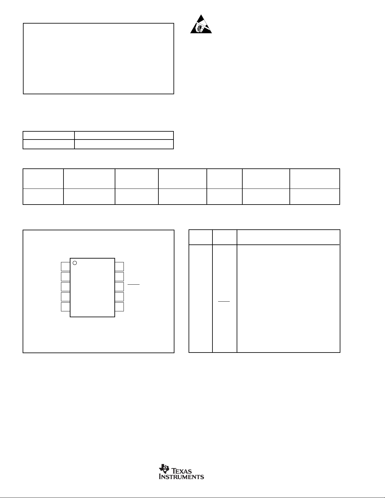
PIN CONFIGURATION
Top View MSOP
GND
VREFP
VREFN
AINN
AINP
1
2
3
4
5
ADS1244
10
9
8
7
6
CLK
SCLK
DRDY/DOUT
DVDD
AVDD
PIN DESCRIPTIONS
PIN
NUMBER NAME DESCRIPTION
1 GND Analog and Digital Ground
2 VREFP Positive Reference Input
3 VREFN Negative Reference Input
4 AINN Negative Analog Input
5 AINP Positive Analog Input
6 AVDD Analog Power Supply, 2.5V to 5.25V
7 DVDD Digital Power Supply, 1.8V to 3.6V
8 DRDY/ Dual-Purpose Output:
DOUT Data Ready: Indicates valid data by going LOW.
Data Output: Outputs data, MSB first, on the first
rising edge of SCLK.
9 SCLK Serial Clock Input: Clocks out data on the rising
edge. Used to initiate calibration and Sleep Mode,
see text for more details.
10 CLK System Clock Input: Typically 2.4576MHz
2
www.ti.com
ADS1244
SBAS273
ELECTRICAL CHARACTERISTICS
All specifications –40°C to +85°C, AVDD = 5V, DVDD = +3V, f
PARAMETER CONDITIONS MIN TYP MAX UNITS
ANALOG INPUT
Full-Scale Input Voltage Range
Absolute Input Range AINP, AINN with Respect to GND GND – 0.1
Differential Input Impedance f
SYSTEM PERFORMANCE
Resolution No Missing Codes 24 Bits
Data Rate f
Integral Nonlinearity (INL) Differential Input Signal, End Point Fit ±0.0002 ±0.0008 % FSR
Offset Error 1 10 ppm of FSR
Offset Error Drift
Gain Error 0.005 0.02 %
Gain Error Drift
Common-Mode Rejection at DC 90 130 dB
Normal-Mode Rejection f
Input Referred Noise 1 ppm of FSR, rms
(3)
(3)
(4)
f
= 50 ± 1Hz, f
CM
f
= 60 ± 1Hz, f
CM
(5)
= 50 ± 1Hz, f
SIG
f
= 60 ± 1Hz, f
SIG
Analog Power-Supply Rejection at DC, ∆AVDD = 5% 105 dB
Digital Power-Supply Rejection at DC, ∆DVDD = 5% 100 dB
VOLTAGE REFERENCE INPUT
Reference Input Voltage (V
Negative Reference Input (VREFN) GND – 0.1 VREFP – 0.5 V
)V
REF
REF
Positive Reference Input (VREFP) VREFN + 0.5 AVDD + 0.1 V
Voltage Reference Impedance f
DIGITAL INPUT/OUTPUT
Logic Levels
V
(CLK, SCLK) 2.1 5.25 V
IH
V
(CLK, SCLK) GND 0.9 V
IL
V
(
DRDY/DOUT
OH
V
(
DRDY/DOUT
OL
Input Leakage (CLK, SCLK) 0 < (CLK, SCLK) < DVDD ±10 µA
CLK Frequency (f
CLK Duty Cycle 30 70 %
)I
)I
) 6MHz
CLK
POWER SUPPLY
AVDD 2.5 5.25 V
DVDD 1.8 3.6 V
AVDD Current Sleep Mode 0.1 1 µA
DVDD Current Sleep Mode, CLK Stopped 0.1 µA
Sleep Mode, 2.4576MHz CLK Running 1.3 5 µA
Total Power Dissipation AVDD = DVDD = 3V 270 µW
NOTES: (1) sps = Samples Per Second. (2) FSR = Full-Scale Range = 4V
of the common-mode input. (5) f
is the frequency of the input signal. (6) It will not be possible to reach the digital output full-scale code when V
SIG
= 2.4576MHz, and V
CLK
= 2.5V, unless otherwise specified.
REF
ADS1244
AINP – AINN
= 2.4576MHz 5 MΩ
CLK
= 2.4576MHz 15 sps
CLK
±2V
REF
AVDD + 0.1
0.01 ppm of FSR/°C
0.5 ppm/°C
= 2.4576MHz 100 dB
CLK
= 2.4576MHz 100 dB
CLK
= 2.4576MHz 60 dB
CLK
= 2.4576MHz 70 dB
CLK
≡ VREFP – VREFN 0.5 2.5 AVDD
= 2.4576MHz 1 MΩ
CLK
= 1mA 2.6 V
OH
= 1mA 0.4 V
OL
(6)
AVDD = 3V 85 µA
AVDD = 5V 90 150 µA
DVDD = 3V
. (3) Recalibration can reduce these errors to the level of the noise. (4) fCM is the frequency
REF
4.5 10 µA
REF
V
V
(1)
V
> AVDD/2.
(2)
ADS1244
SBAS273
www.ti.com
3
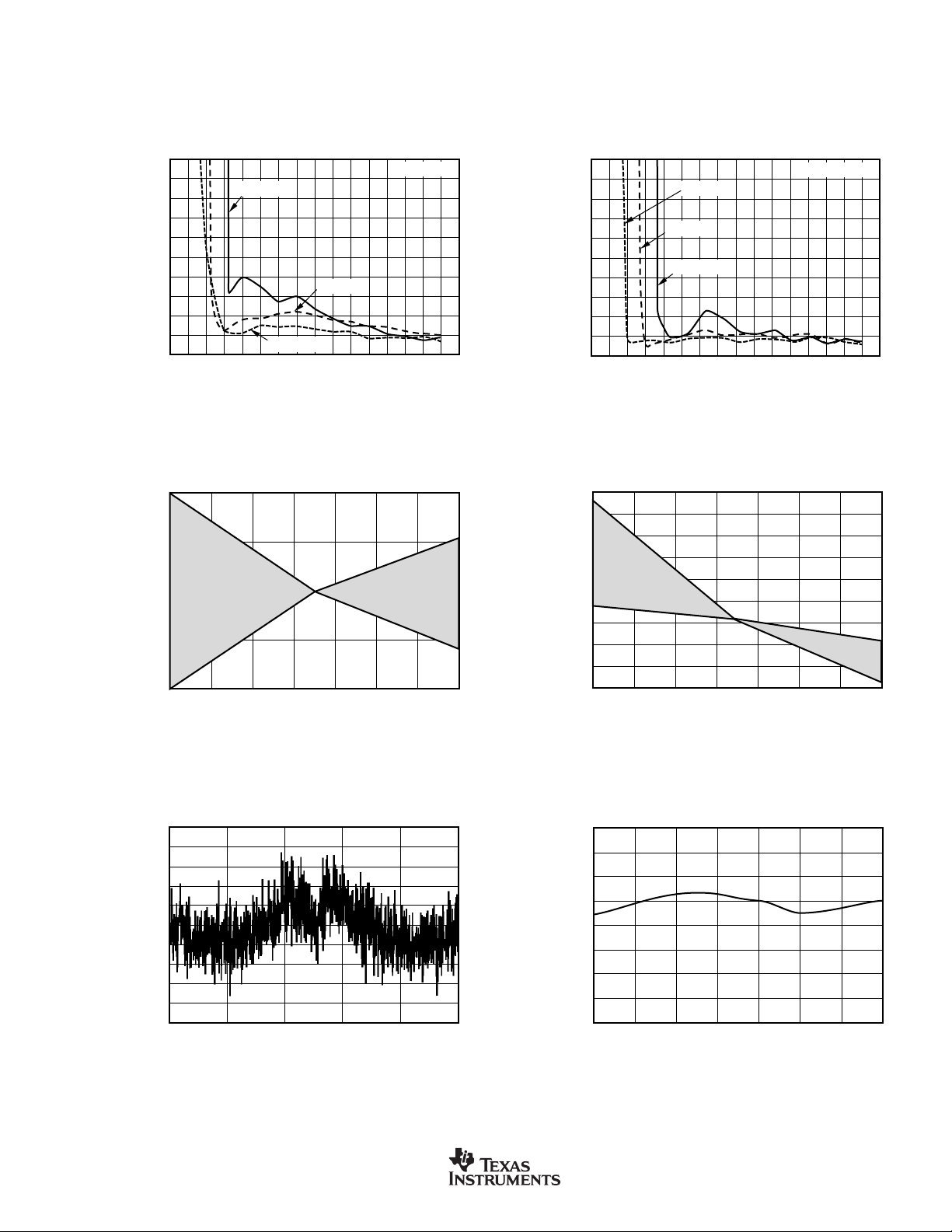
TYPICAL CHARACTERISTICS
At TA = +25°C, AVDD = +5V, DVDD = +3V, f
= 2.4576MHz, and V
CLK
= +2.5V, unless otherwise specified.
REF
110
105
12
10
100
ANALOG CURRENT vs TEMPERATURE
95
AVDD = 5V, f
90
85
Current (µA)
= 4.9152MHz
CLK
8
6
Current (µA)
4
DIGITAL CURRENT vs TEMPERATURE
DVDD = 3V, f
= 4.9152MHz
CLK
80
75
AVDD = 3V, f
70
15–5–25 35 55 75 95–45
Temperature (°C)
ANALOG CURRENT vs ANALOG SUPPLY
94
92
90
f
= 4.9152MHz
CLK
88
86
Current (µA)
84
82
80
3 3.5 4
Analog Supply (V)
= 2.4576MHz
CLK
f
CLK
4.5 5
= 2.4576MHz
2
DVDD = 1.8V, f
= 2.4576MHz
CLK
0
15–5–25 35 55 75 95–45
Temperature (°C)
DIGITAL CURRENT vs DIGITAL SUPPLY
20
18
16
14
12
10
f
= 4.9152MHz
CLK
8
Current (µA)
6
4
2
0
5.52.5
2 2.5 3
f
= 2.4576MHz
CLK
3.5
41.5
Digital Supply (V)
INL (ppm of FSR)
4
3
2
T = 25°C
AVDD = 5V, V
1
0
–1
INTEGRAL NONLINEARITY vs V
–2
T = 85°C
–3
IN
T = –40°C
REF
= 2.5V
3
2
1
0
–1
INL (ppm of FSR)
–2
T = 85°C
–3
1–1–335–5
VIN (V)
INTEGRAL NONLINEARITY vs V
AVDD = 3V, V
T = –40°C
T = 25°C
0.5–0.5–1.5 1.5 2.5–2.5
VIN (V)
IN
REF
= 1.25V
ADS1244
www.ti.com
SBAS273
TYPICAL CHARACTERISTICS (Cont.)
INTEGRAL NONLINEARITY vs ANALOG SUPPLY
Analog Supply (V)
INL (ppm of FSR)
1.5 2 2.5 3 3.5 4 4.5 5 5.5
20
18
16
14
12
10
8
6
4
2
0
T = 25°C
T = 85°C
T = –40°C
V
REF
= AVDD/2
GAIN vs TEMPERATURE
Temperature (°C)
Normalized Gain
15–5–25 35 55 75 95–45
1.00008
1.00006
1.00004
1.00002
1
0.99998
0.99996
0.99994
0.99992
0.9999
NOISE vs TEMPERATURE
Temperature (°C)
Noise (ppm of FSR, rms)
–25 –515
35 55 75
95–45
1.6
1.4
1.2
1.0
0.8
0.6
0.4
0.2
0
At TA = +25°C, AVDD = +5V, DVDD = +3V, f
INTEGRAL NONLINEARITY vs ANALOG SUPPLY
20
18
16
14
12
10
8
INL (ppm of FSR)
6
4
2
0
1.5 2 2.5 3 3.5 4 4.5 5 5.5
T = –40°C
T = 85°C
Analog Supply (V)
= 2.4576MHz, and V
CLK
T = 25°C
V
REF
= AVDD
= +2.5V, unless otherwise specified.
REF
1
0.5
0
–0.5
Normalized Offset (ppm of FSR)
–1
1.6
1.5
1.4
1.3
1.2
1.1
1
0.9
Noise (ppm of FSR, rms)
0.8
0.7
0.6
ADS1244
SBAS273
OFFSET vs TEMPERATURE
Temperature (°C)
NOISE vs INPUT SIGNAL
–3 –11
15–5–25 35 55 75 95–45
3
V
(V)
IN
5–5
www.ti.com
5
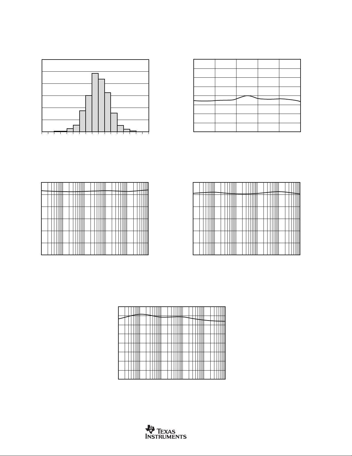
TYPICAL CHARACTERISTICS (Cont.)
At TA = +25°C, AVDD = +5V, DVDD = +3V, f
= 2.4576MHz, and V
CLK
= +2.5V, unless otherwise specified.
REF
1200
1000
800
600
400
Number of Occurences
200
0
–3 –2 –10 1 2 3 4–4
120
100
80
60
HISTOGRAM OF OUTPUT DATA
ppm of FSR
ANALOG PSRR vs FREQUENCY
14
13
12
11
10
Input-Referred Noise (µV, rms)
120
100
80
60
INPUT-REFERRED NOISE vs V
9
8
7
6
V
(V)
REF
DIGITAL PSRR vs FREQUENCY
REF
321450
Magnitude (dB)
40
20
0
1k10010 10k 100k1
Frequency (Hz)
160
140
120
100
80
60
Magnitude (dB)
40
20
0
Magnitude (dB)
40
20
0
CMRR vs FREQUENCY
1k10010 10k 100k1
Frequency (Hz)
1k10010 10k 100k1
Frequency (Hz)
6
www.ti.com
ADS1244
SBAS273

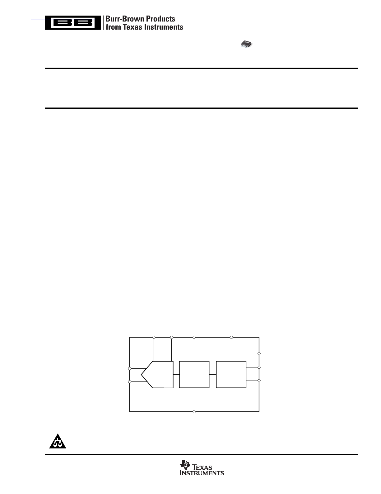
OVERVIEW
The ADS1244 is an A/D converter comprised of a 3rd-order
modulator followed by a digital filter. The modulator measures
the differential input signal V
differential reference V
shows a conceptual diagram. The differential reference is
scaled internally so that the full-scale input range is
The digital filter receives the modulator’s signal and provides
a low-noise digital output. The filter also sets the frequency
response of the converter and provides 50Hz and 60Hz
rejection while settling in a single conversion cycle. A 2-wire
serial interface indicates conversion completion and provides
the user with the output data.
= (AINP – AINN) against the
IN
= (VREFP – VREFN). Figure 1
REF
±2V
REF
ESD Protection
AVDD
AINP
.
AINN
AVDD
AVDD/2
C
= 4pF
A1
S
S
AVDD/2
2
C
= 8pF
B
2
C
= 4pF
A2
S
1
S
1
VREFP VREFN
Σ
V
REF
2
2V
REF
AINP
AINN
V
IN
Σ
Modulator
Digital
Filter and
Serial
Interface
FIGURE 1. Conceptual Diagram of the ADS1244.
CLK
DRDY/DOUT
SCLK
ANALOG INPUTS (AINP, AINN)
The input signal to be measured is applied to the input pins
AINP and AINN. The ADS1244 accepts differential input
signals, but can also measure unipolar signals. When measuring unipolar (or “single-ended” signals) with respect to
ground, connect the negative input (AINN) to ground and
connect the input signal to the positive input (AINP). Note
that when the ADS1244 is used this way, only half of the
converter’s full-scale range is used since only positive digital
output codes will be produced.
The ADS1244 measures the input signal using internal
capacitors that are continuously charged and discharged.
Figure 2 shows a simplified schematic of the ADS1244’s
input circuitry with Figure 3 showing the ON/OFF timings of
the switches. S
phase. With S
AINN, and C
phase, S
discharge to approximately AVDD/2 and CB discharges to
0V. This 2-phase sample/discharge cycle repeats with a
frequency of f
switches close during the input sampling
1
closed, CA1 charges to AINP, CA2 charges to
1
charges to (AINP – AINN). For the discharge
B
opens first and then S2 closes. CA1 and C
1
/128 (19.2kHz for f
CLK
= 2.4576MHz).
CLK
A2
FIGURE 2. Simplified Input Structure.
t
= 128/f
SAMPLE
ON
S
1
OFF
ON
S
2
OFF
CLK
FIGURE 3. S1 and S2 Switch Timing for Figure 1.
The constant charging of the input capacitors presents a load
on the inputs that can be represented by effective impedances. Figure 4 shows the input circuitry with the capacitors
and switches of Figure 2 replaced by their effective impedances. These impedances scale inversely with f
quency. For example, if f
’s frequency is reduced by a
CLK
CLK
fre-
factor of 2, the impedances will double.
AVDD/2
= 13MΩ
= 6.5MΩ
= 13MΩ
= 2.4576MHz.
CLK
(1)
(1)
(1)
AINP
AINN
AVDD/2
ZeffA = t
ZeffB = t
ZeffA = t
SAMPLE/CA1
SAMPLE/CB
SAMPLE/CA2
NOTE: (1) f
FIGURE 4. Effective Analog Input Impedances.
ESD diodes protect the inputs. To keep these diodes from turning
on, make sure the voltages on the input pins do not go below
GND by more than 100mV, and likewise do not exceed AVDD by
100mV: GND – 100mV < (AINP, AINN) < AVDD + 100mV.
ADS1244
SBAS273
www.ti.com
7

VOLTAGE REFERENCE INPUTS (VREFP, VREFN)
The voltage reference used by the modulator is generated
from the voltage difference between VREFP and VREFN:
V
= VREFP – VREFN. The reference inputs use a structure
REF
similar to that of the analog inputs. A simplified diagram of the
circuitry on the reference inputs is shown in Figure 5. The
switches and capacitors can be modeled with an effective
t
SAMPLE
AVDD
impedance =
FIGURE 5. Simplified Reference Input Circuitry.
ESD diodes protect the reference inputs. To prevent
these diodes from turning on, make sure the voltages on
the reference pins do not go below GND by more than
100mV, and likewise do not exceed AVDD by 100mV:
GND – 100mV < (VREFP, VREFN) < AVDD + 100mV.
V
is typically AVDD/2, but it can be raised as high as
REF
AVDD. When V
to reach the full-scale digital output value corresponding to
±2V
since this would require the analog inputs to exceed
REF
the power supplies.
positive full-scale signal is 10V. The maximum positive input
signal that can be supplied before the ESD diodes begin to turn
on is when AINP = 5.1V and AINN = –0.1V → V
Therefore, it will not be possible to reach the positive (or
negative) full-scale readings in this configuration. The digital
output codes will be limited to approximately one half of the
entire range.
For best performance, bypass the voltage reference inputs
with a 0.1µF capacitor between VREFP and VREFN. Place
the capacitor as close as possible to the pins.
/
pF
25
2
VREFP VREFN
exceeds AVDD/2, it will not be possible
REF
For example, if V
S
1
= 1MΩ for f
25pF
S
2
= 2.4576MHz.
CLK
AVDD
S
REF
1
ESD
Protection
= AVDD = 5V, the
IN
= 5.2V.
Minimize the overshoot and undershoot on CLK for the best
analog performance. A small resistor in series with CLK (10Ω
to 100Ω) can often help. CLK can be generated from a number
of sources including stand-alone crystal oscillators and
microcontrollers. The MSP430, an ultra low power
microcontroller, is especially well suited for this task. Using the
MSP430’s FLL clock generator available on the 4xx family, it’s
easy to produce a 2.4576MHz clock from a 32.768kHz crystal.
DATA READY/DATA OUTPUT (
DRDY/DOUT
)
This digital output pin serves two purposes. It indicates when
new data is ready by going LOW. Afterwards, on the first rising
edge of SCLK, the DRDY/DOUT
pin changes function and
begins outputting the conversion data, MSB first. Data is
shifted out on each subsequent SCLK rising edge. After all 24
bits have been retrieved, the pin can be forced HIGH with an
additional SCLK. It will then stay HIGH until new data is ready.
This is useful when polling on the status of DRDY/DOUT
to
determine when to begin data retrieval.
SERIAL CLOCK INPUT (SCLK)
This digital input shifts serial data out with each rising edge.
As with CLK, this input may be driven with 5V logic regardless of the DVDD or AVDD voltage. There is hysteresis built
into this input, but care should still be taken to ensure a clean
signal. Glitches or slow rising signals can cause unwanted
additional shifting. For this reason, it is best to make sure the
rise-and-fall times of SCLK are less than 50ns.
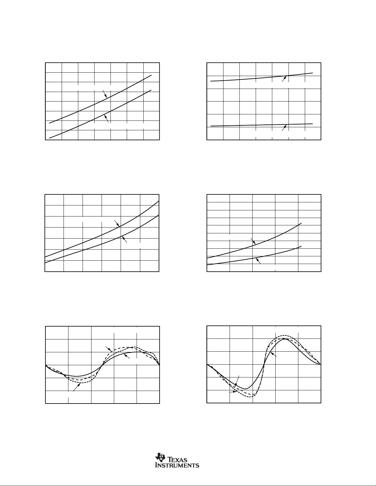
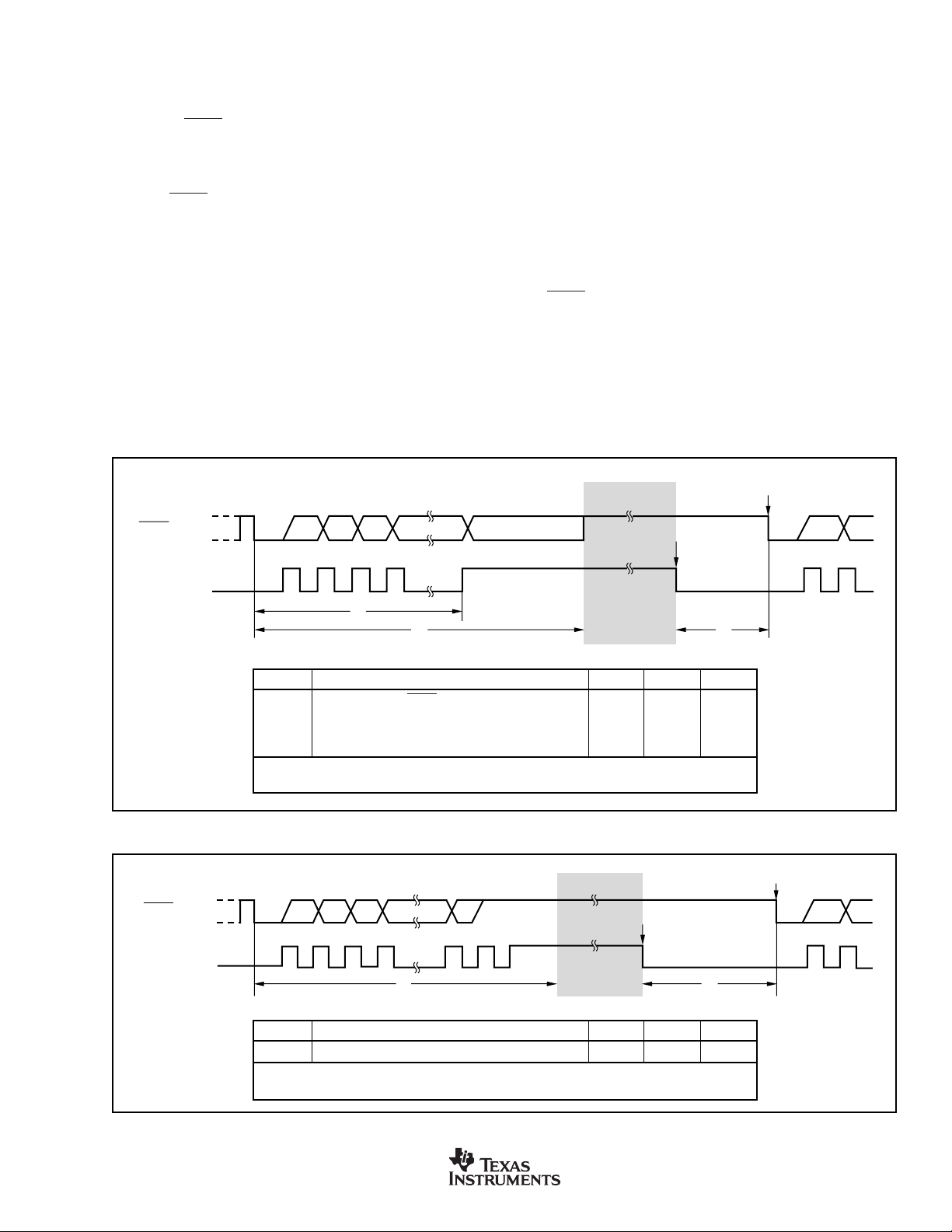
FREQUENCY RESPONSE
The ADS1244’s frequency response for f
shown in Figure 6. The frequency response repeats at multiples of 19.2kHz. The overall response is that of a low-pass
filter with a –3dB cutoff frequency of 13.7Hz. As can be seen,
the ADS1244 does a good job attenuating out to 19kHz. For
the best resolution, limit the input bandwidth to below this value
to keep higher frequency noise from affecting performance.
Often a simple RC filter on the ADS1244’s analog inputs is all
that is needed.
FREQUENCY RESPONSE
f
= 2.4576MHz
0
–20
–40
CLK
= 2.4576MHz is
CLK
CLOCK INPUT (CLK)
This digital input supplies the system clock to the ADS1244.
The recommended CLK frequency is 2.4576MHz. This places
the notches of the digital filter at 50Hz and 60Hz and sets the
data rate at 15SPS. The CLK frequency can be increased to
speed up the data rate, but the frequency notches will move
in frequency proportionally. CLK must be left running during
normal operation. It may be turned off during Sleep Mode to
save power, but this is not required. The CLK input may be
driven with 5V logic, regardless of the DVDD or AVDD voltage.
8
www.ti.com
–60
–80
Gain (dB)
–100
–120
–140
Frequency (kHz)
FIGURE 6. Frequency Response.
9.6 19.20
ADS1244
SBAS273

To help see the response at lower frequencies, Figure 7
SETTLING ERROR vs DELAY TIME
f
CLK
= 2.4576MHz
Delay Time, t
DELAY
(ms)
Settling Error (%)
2 4 6 8 10 12 14 160
10.000000
1.000000
0.100000
0.010000
0.001000
0.000100
0.000010
0.000001
illustrates the response out to 180Hz. Notice that both 50Hz
and 60Hz signals are rejected. This feature is very useful for
eliminating power line cycle interference during measurements. Figure 8 shows the ADS1244’s response around
these frequencies.
0
–20
–40
–60
–80
–100
Gain (dB)
–120
–140
–160
–180
FREQUENCY RESPONSE TO 180Hz
0
102030405060708090
f
= 2.4576MHz
CLK
Frequency (Hz)
100
110
120
130
140
150
160
170
180
FIGURE 7. Frequency Response to 180Hz.
The ADS1244’s data rate and frequency response scale
directly with CLK frequency. For example, if f
increases
CLK
from 2.4576MHz to 4.9152MHz, the data rate increases from
15sps to 30sps while the notches in the response at 50Hz
and 60Hz move out to 100Hz and 120Hz.
SETTLING TIME
The ADS1244 has single-cycle settling. That is, the output
data is fully settled after a single conversion—there is no
need to wait for additional conversions before retrieving the
data when there is a change on the analog inputs.
In order to realize single-cycle settling, synchronize changes
on the analog inputs to the conversion beginning, which is
indicated by the falling edge of DRDY/DOUT
when using a multiplexer in front of the ADS1244, change the
multiplexer’s inputs when DRDY/DOUT
ing the time between the conversion beginning and the
change on the analog inputs (t
) will result in a settling
DELAY
error in the conversion data, as shown in Figure 9. The
settling error versus delay time is shown in Figure 10. If the
input change is delayed to the point where the settling error
is too high, simply ignore the first data result and wait for the
second conversion which will be fully-settled.
. For example,
goes LOW. Increas-
–40
–50
–60
–70
–80
Gain (dB)
–90
–100
–110
–120
FREQUENCY RESPONSE NEAR 50Hz AND 60Hz
50 55 60 6545
f
= 2.4576MHz
CLK
Frequency (Hz)
FIGURE 8. Frequency Response Near 50Hz and 60Hz.
Begin New Conversion,
Complete Previous Conversion
DRDY/DOUT
V
IN
t
DELAY
Previous Conversion Data
FIGURE 10. Settling Error vs Delay Time.
New Conversion Complete
FIGURE 9. Analog Input Change Timing.
ADS1244
SBAS273
www.ti.com
9

POWER-UP
Self-calibration is performed at power-up to minimize offset and
gain errors. In order for the self-calibration at power-up to work
properly, make sure that both AVDD and DVDD increase
monotonically and are settled by t
, as shown in Figure 11.
1
SCLK must be held LOW during this time. Once calibration is
complete,
for retrieval. The time required before the first data is ready (t
DRDY/DOUT
will go LOW indicating data is ready
6
depends on how fast AVDD and DVDD ramp to their final value
(t
). For most ramp rates, t1 + t2 ≈ 350ms (f
1
= 2.4576MHz).
CLK
If the system environment is not stable during power-up (the
temperature is varying or the supply voltages are moving
around), it is recommended that a self-calibration be issued
after everything is stable.
DATA FORMAT
The ADS1244 outputs 24 bits of data in Binary Two’s
Complement format. The Least Significant Bit (LSB) has a
weight of (2V
)/(223 – 1). A positive full-scale input pro-
REF
duces an output code of 7FFFFFH and the negative full-scale
input produces an output code of 800000
. The output clips
H
at these codes for signals exceeding full-scale. Table I
summarizes the ideal output codes for different input signals.
INPUT SIGNAL VIN (AINP – AINN) IDEAL OUTPUT CODE
≥ +2V
)
≤−
NOTE: (1) Excludes effects of noise, INL, offset, and gain errors.
REF
+−2
V
REF
23
21
0 000000
−−2
V
REF
23
21
23
V
REF
2
23
−
21
2
7FFFFF
000001
FFFFFF
800000
TABLE I. Ideal Output Code versus Input Signal.
(1)
H
H
H
H
H
AVDD and DVDD
DRDY/DOUT
SCLK
SYMBOL DESCRIPTION MIN MAX UNITS
(1)
t
1
(1)
t
2
NOTE: (1) Values given for f
to CLK period.
FIGURE 11. Power-Up Timing.
Data ready after power-up calibration.
t
1
AVDD and DVDD settling time. 100 ms
Wait time for calibration and first data conversion. 316 ms
= 2.4576MHz. For different CLK frequencies, scale proportional
CLK
t
2
10
www.ti.com
ADS1244
SBAS273

DATA RETRIEVAL
The ADS1244 continuously converts the analog input signal.
To retrieve data, wait until DRDY/DOUT
shown in Figure 12. After this occurs, begin shifting out the
data by applying SCLKs. Data is shifted out Most Significant
Bit (MSB) first. It is not required to shift out all the 24 bits of
data, but the data must be retrieved before the new data is
updated (see t
DRDY/DOUT 23 22 21
) or else it will be overwritten. Avoid data
3
Data is ready.
goes LOW, as
retrieval during the update period. DRDY/DOUT
at the state of the last bit shifted out until it is taken HIGH (see
t
), indicating that new data is being updated.
7
To avoid having DRDY/DOUT
remain in the state of the last
bit, shift a 25th SCLK to force DRDY/DOUT
Figure 13. This technique is useful when a host controlling
the ADS1244 is polling DRDY/DOUT
to determine when
data is ready.
Data
New data is ready.
LSBMSB
0
will remain
HIGH, see
SCLK
SYMBOL DESCRIPTION MIN MAX UNITS
t
DRDY/DOUT
3
t
SCLK positive or negative pulse width. 100 ns
4
(1)
t
SCLK rising edge to new data bit valid: 50 ns
5
propagation delay.
t
SCLK rising edge to old data bit valid: hold time. 0 ns
6
(2)
t
Data updating, no read back allowed. 152 152 µs
7
(2)
t
Conversion time (1/data rate). 66.667 66.667 ms
8
NOTES: (1) Load on
CLK frequencies, scale proportional to CLK period. For example, for f
FIGURE 12. Data Retrieval Timing.
Data is ready.
DRDY/DOUT
t
5
t
3
124
LOW to first SCLK rising edge. 0 ns
DRDY/DOUT
= 20pF || 100kΩ. (2) Values given for f
23
t
4
t
4
t
8
Data
22 21 0
t
6
= 2.4576MHz. For different
CLK
= 4.9152MHz, t8 → 33.333ms.
CLK
t
7
New data is ready.
SCLK
12425
25th SCLK to force DRDY/DOUT HIGH.
FIGURE 13. Data Retrieval with DRDY/DOUT Forced HIGH Afterwards.
ADS1244
SBAS273
www.ti.com
11

SELF-CALIBRATION
The user can initiate self-calibration at any time, though in
many applications the ADS1244’s drift performance is good
enough that the self-calibration performing automatically at
power-up is all that is needed. To initiate a self-calibration,
apply at least two additional SCLKs after retrieving 24 bits of
data. Figure 14 shows the timing pattern. The 25th SCLK will
send DRDY/DOUT
will begin the calibration cycle. Additional SCLK pulses may
be sent after the 26th SCLK, but try to minimize activity on
SCLK during calibration for best results.
HIGH. The falling edge of the 26th SCLK
When the calibration is complete,
DRDY/DOUT
will go LOW
indicating that new data is ready. There is no need to alter the
analog input signal applied to the ADS1244 during calibration,
the inputs pins are disconnected within the A/D converter and
the appropriate signals applied internally automatically. The
first conversion after a calibration is fully settled and valid for
use. The time required for a calibration depends on two
independent signals: the falling edge of SCLK and an internal
clock derived from CLK. Variations in the internal calibration
values will change the time required for calibration (t
the range given by the MIN/MAX specs. t
and t13 described
12
) within
9
in the next section are affected likewise.
Data ready after cal.
23DRDY/DOUT
SCLK
SYMBOL DESCRIPTION MIN MAX UNITS
NOTE: (1) Values given for f
period.
124
(1)
t
First data ready after calibration. 209 210 ms
9
FIGURE 14. Self-Calibration Timing.
Cal begins.
25 26
t
9
= 2.4576MHz. For different CLK frequencies, scale proportional to CLK
CLK
2322 21 0
12
www.ti.com
ADS1244
SBAS273
SLEEP MODE
DRDY/DOUT
Sleep Mode dramatically reduces power consumption (typically < 1µW with CLK stopped) by shutting down all of the
active circuitry. To enter Sleep Mode, simply hold SCLK
HIGH after DRDY/DOUT
goes LOW, as shown in Figure 15.
Sleep Mode can be initiated at any time during read back; it
is not necessary to retrieve all 24 bits of data beforehand.
Once t
activate. DRDY/DOUT
has passed with SCLK held HIGH, Sleep Mode will
11
stays HIGH once Sleep Mode begins.
SCLK must remain HIGH to stay in Sleep Mode. To exit
Sleep Mode (“wakeup”), set SCLK LOW. The first data after
exiting Sleep Mode is valid. It is not necessary to stop CLK
during Sleep Mode, but doing so will further reduce the digital
supply current.
Sleep Mode With Self-Calibration
Self-calibration can be set to run immediately after exiting
Sleep Mode. This is useful when the ADS1244 is put in Sleep
Mode for long periods of time and self-calibration is desired
afterwards to compensate for temperature or supply voltage
changes.
To force a self-calibration with Sleep Mode, shift 25 bits out
before taking SCLK HIGH to enter Sleep Mode. Self-calibration will then begin after wakeup. Figure 16 shows the
appropriate timing. Note the extra time needed after wakeup
for calibration before data is ready. The first data after Sleep
Mode with self-calibration is fully-settled and can be used.
SINGLE CONVERSIONS
When only single conversions are needed, Sleep Mode can
be used to start and stop the ADS1244. To make a single
conversion, first enter the Sleep Mode holding SCLK HIGH.
Now, when ready to start the conversion, take SCLK LOW.
The ADS1244 will wake up and begin the conversion. Wait
for
Afterwards, take SCLK HIGH to stop the ADS1244 from
converting and re-enter Sleep Mode. Continue to hold SCLK
HIGH until ready to start the next conversion. Operating in
this fashion greatly reduces power consumption since the
ADS1244 is shut down while idle between conversions. Selfcalibrations can be performed prior to the start of the single
conversions by using the waveform shown in Figure 16.
to go LOW, and then retrieve the data.
DRDY/DOUT 23 22 21
SCLK
124
t
10
SYMBOL DESCRIPTION MIN MAX UNITS
(1)
t
t
t
NOTE: (1) Values given for f
period.
SCLK HIGH after
10
Sleep Mode.
(1)
Sleep Mode activation Time. 66.5 66.5 ms
11
(1)
Data ready after wakeup. 71 72 ms
12
t
11
DRDY/DOUT
= 2.4576MHz. For different CLK frequencies, scale proportional to CLK
CLK
023
goes LOW to activate 0 63.7 ms
FIGURE 15. Sleep Mode Timing; Can be Used for Single Conversions.
DRDY/DOUT 23
22 21 0 23
Sleep Mode
Sleep Mode
Data ready after wakeup.
Wakeup
t
12
Data ready after wakeup and cal.
Wakeup and begin cal.
SCLK
12425
t
11
SYMBOL DESCRIPTION MIN MAX UNITS
(1)
t
NOTE: (1) Values given for f
period.
Data ready after wakeup and calibration. 210 211 ms
13
= 2.4576MHz. For different CLK frequencies, scale proportional to CLK
CLK
t
13
FIGURE 16. Sleep Mode with Self-Calibration on Wakeup Timing; Can be Used for Single Conversions.
ADS1244
SBAS273
www.ti.com
13

SINGLE-SUPPLY OPERATION
DRDY/DOUT
It is possible to operate the ADS1244 with a single supply.
For a 3V supply, simply connect AVDD and DVDD together.
Figure 17 shows an example of the ADS1244 running on a
single 5V supply. An external resistor, R1, is used to drop 5V
supply down to a desired voltage level of DVDD. For example, if the desired DVDD supply voltage is 3V and AVDD
is 5V, the value of R1 should be:
R1 = (5V – 3V)/4.5µA ≈ 440kΩ
where 4.5µA is a typical digital current consumption when
DVDD = 3V (refer to the typical characteristic “Digital Current
vs Digital Supply”). A buffer on DRDY/DOUT
level-shifting if required.
DVDD can be set to a desired voltage by choosing a proper
value of R1, but keep in mind that DVDD must be set
between 1.8V and 3.6V. Note that the maximum logic HIGH
output of DRDY/DOUT
is equal to DVDD, but both CLK and
SCLK inputs can be driven with 5V logic regardless of the
DVDD or AVDD voltage. Use 0.1µF capacitors to bypass
both AVDD and DVDD.
to +5V logic
SN74LVCC3245A
can provide
+5V
MULTICHANNEL SYSTEMS
Multiple ADS1244s can be operated in parallel to measure
multiple input signals. Figure 18 shows an example of a
2-channel system. For simplicity, the supplies and reference
circuitry were not included. The same CLK signal should be
applied to all devices. To be able to synchronize the
ADS1244s, connect the same SCLK signal to all devices as
well. When ready to synchronize, place all the devices in
Sleep Mode. Afterwards, “wakeup” and all the ADS1244s will
be synchronized. That is, they will sample the input signals
simultaneously.
The
same time after synchronization. The falling edges indicating
that new data is ready will vary with respect to each other no
more than timing specification t
posible differences in the ADS1244’s internal calibration
settings. To account for this when using multiple devices,
either wait for t
DRDY/DOUT
gone LOW before retrieving data.
IN1
outputs will go LOW at approximately the
. This variation is due to
14
to pass after seeing one device’s
14
go LOW, or wait until all DRDY/DOUTs have
ADS1244
1
2
3
4
5
GND
VREFP
VREFN
AINN
AINP
CLK
SCLK
DRDY/DOUT
DVDD
AVDD
10
9
8
7
6
OUT1
from
+5V logic
109876
CLK SCLK DRDY/DOUT DVDD AVDD
GND VREFP VREFN AINN AINP
12345
from
+5V logic
ADS1244
0.1µF
++
R1
0.1µF
FIGURE 17. Example of the ADS1244 Running on a Single
5V Supply.
ADS1244
GND
1
VREFP
2
VREFN
3
AINN
IN2
OUT1
OUT2
SYMBOL DESCRIPTION MIN MAX UNITS
4
AINP
5
t
Difference between
14
going LOW in multichannel systems.
CLK
SCLK
DRDY/DOUT
DVDD
AVDD
t
14
DRDY/DOUT
10
9
8
7
6
CLK and SCLK
Sources
s
OUT2
±500 µs
FIGURE 18. Example of Using Multiple ADS1244s in Parallel.
14
www.ti.com
ADS1244
SBAS273

WEIGH SCALE SYSTEM
Figure 19 shows an example of a weigh scale system. OPA1,
OPA2, R
load cell output. The gain is equal to (1 + 2 R
ing on the load cell, the typical gain setting is from 100 to 250.
R
and CI form a single-pole low-pass filter to band-limit the
I
, and RF form a differential gain stage to amplify the
G
F/RG
). Depend-
differential gain stage noise and reduce mechanical vibration
noise from the load cell. The cutoff frequency of the low-pass
filter should be as low as possible to minimize the overall
system noise. The reference voltage is typically generated by
dividing down the supply voltage (R
VR1
, R
). Use a bypass
VR2
capacitor located as close to VREFP as possible.
Load Cell
EMI Filter
EMI Filter
EMI Filter
EMI Filter
5V
R
VR1
0.1µF
(1)
OPA1
R
F
R
G
R
F
(1)
OPA2
NOTE: (1) OPA2335 or OPA2277 recommended.
R
VR2
VREFP
R
I
R
I
AINP
C
I
AINN
0.1µF1µF 0.1µF 1µF
AVDD
VREFN GND
DVDD
ADS1244
SCLK
DRDY/ DOUT
CLK
DVCC
MSP430Fx41x
P1.2/TA1
P1.0/TA0
P1.1/TA0/MCLK
AVSS
1.8V ~ 3.6V
AVCC
XIN
XOUT/TCLK
DVSS
0.1µF
32.768kHz
FIGURE 19. Weigh Scale System.
ADS1244
SBAS273
www.ti.com
15

SUMMARY OF SERIAL INTERFACE WAVEFORMS
DRDY/DOUT
SCLK
DRDY/DOUT
SCLK
DRDY/DOUT
SCLK
23 22 21 0
MSB LSB
124
a. Data Retrieval.
23 22 21 0
12425
b. Data Retrieval with DRDY/DOUT Forced HIGH Afterwards.
23 22 21 0
1242526
Begin cal.
Data ready after cal.
DRDY/DOUT
SCLK
DRDY/DOUT
SCLK
c. Self-Calibration.
Data ready.
Sleep Mode
23 22 21 0
Wakeup and
start conversion.
124
d. Sleep Mode/Single Conversions.
Data ready after
wakeup and cal.
Sleep Mode
23 22 21 0
Wakeup and
begin cal.
12425
e. Sleep Mode/Single Conversions with Self-Calibration on Wakeup.
FIGURE 20. Summary of Serial Interface Waveforms.
16
www.ti.com
ADS1244
SBAS273

PACKAGE DRAWING
DGS (S-PDSO-G10) PLASTIC SMALL-OUTLINE PACKAGE
0,69
0,41
0,25
0,15 NOM
Gage Plane
4073272/B 08/01
4,98
0,17
6
3,05
4,78
2,95
10
5
3,05
2,95
1
0,27
0,15
0,05
1,07 MAX
Seating Plane
0,10
0,50
M
0,08
0°–6°
NOTES: A. All linear dimensions are in millimeters.
B. This drawing is subject to change without notice.
C. Body dimensions do not include mold flash or protrusion.
A. Falls within JEDEC MO-187
ADS1244
SBAS273
www.ti.com
17

PACKAGE OPTION ADDENDUM
www.ti.com
3-Oct-2003
PACKAGING INFORMATION
ORDERABLE DEVICE STATUS(1) PACKAGE TYPE PACKAGE DRAWING PINS PACKAGE QTY
ADS1244IDGSR ACTIVE VSSOP DGS 10 2500
ADS1244IDGST ACTIVE VSSOP DGS 10 250
(1) The marketing status values are defined as follows:
ACTIVE: Product device recommended for new designs.
LIFEBUY: TI has announced that the device will be discontinued, and a lifetime-buy period is in effect.
NRND: Not recommended for new designs. Device is in production to support existing customers, but TI does not recommend using this part in
a new design.
PREVIEW: Device has been announced but is not in production. Samples may or may not be available.
OBSOLETE: TI has discontinued the production of the device.

IMPORTANT NOTICE
Texas Instruments Incorporated and its subsidiaries (TI) reserve the right to make corrections, modifications,
enhancements, improvements, and other changes to its products and services at any time and to discontinue
any product or service without notice. Customers should obtain the latest relevant information before placing
orders and should verify that such information is current and complete. All products are sold subject to TI’s terms
and conditions of sale supplied at the time of order acknowledgment.
TI warrants performance of its hardware products to the specifications applicable at the time of sale in
accordance with TI’s standard warranty . Testing and other quality control techniques are used to the extent TI
deems necessary to support this warranty . Except where mandated by government requirements, testing of all
parameters of each product is not necessarily performed.
TI assumes no liability for applications assistance or customer product design. Customers are responsible for
their products and applications using TI components. T o minimize the risks associated with customer products
and applications, customers should provide adequate design and operating safeguards.
TI does not warrant or represent that any license, either express or implied, is granted under any TI patent right,
copyright, mask work right, or other TI intellectual property right relating to any combination, machine, or process
in which TI products or services are used. Information published by TI regarding third-party products or services
does not constitute a license from TI to use such products or services or a warranty or endorsement thereof.
Use of such information may require a license from a third party under the patents or other intellectual property
of the third party , or a license from TI under the patents or other intellectual property of TI.
Reproduction of information in TI data books or data sheets is permissible only if reproduction is without
alteration and is accompanied by all associated warranties, conditions, limitations, and notices. Reproduction
of this information with alteration is an unfair and deceptive business practice. TI is not responsible or liable for
such altered documentation.
Resale of TI products or services with statements different from or beyond the parameters stated by TI for that
product or service voids all express and any implied warranties for the associated TI product or service and
is an unfair and deceptive business practice. TI is not responsible or liable for any such statements.
Following are URLs where you can obtain information on other Texas Instruments products and application
solutions:
Products Applications
Amplifiers amplifier.ti.com Audio www.ti.com/audio
Data Converters dataconverter.ti.com Automotive www.ti.com/automotive
DSP dsp.ti.com Broadband www.ti.com/broadband
Interface interface.ti.com Digital Control www.ti.com/digitalcontrol
Logic logic.ti.com Military www.ti.com/military
Power Mgmt power.ti.com Optical Networking www.ti.com/opticalnetwork
Microcontrollers microcontroller.ti.com Security www.ti.com/security
Telephony www.ti.com/telephony
Video & Imaging www.ti.com/video
Wireless www.ti.com/wireless
Mailing Address: Texas Instruments
Post Office Box 655303 Dallas, Texas 75265
Copyright 2003, Texas Instruments Incorporated
 Loading...