

查询ADS1241-EVM供应商查询ADS1241-EVM供应商
ANALOG-TO-DIGITAL CONVERTER
24-Bit
ADS1242
A
®
D
S
A
1
2
D
4
2
®
S
1
2
4
3
ADS1243
SBAS235B – DECEMBER 2001 – OCTOBER 2004
FEATURES
● 24 BITS NO MISSING CODES
● SIMULTANEOUS 50Hz AND 60Hz REJECTION
(–90dB MINIMUM)
● 0.0015% INL
● 21 BITS EFFECTIVE RESOLUTION
(PGA = 1), 19 BITS (PGA = 128)
● PGA GAINS FROM 1 TO 128
● SINGLE-CYCLE SETTLING
● PROGRAMMABLE DATA OUTPUT RATES
● EXTERNAL DIFFERENTIAL REFERENCE
OF 0.1V TO 5V
● ON-CHIP CALIBRATION
● SPI™ COMPATIBLE
● 2.7V TO 5.25V SUPPLY RANGE
● 600µW POWER CONSUMPTION
● UP TO EIGHT INPUT CHANNELS
● UP TO EIGHT DATA I/O
APPLICATIONS
● INDUSTRIAL PROCESS CONTROL
● LIQUID / GAS CHROMATOGRAPHY
● BLOOD ANALYSIS
● SMART TRANSMITTERS
● PORTABLE INSTRUMENTATION
● WEIGHT SCALES
V
DD
2µA
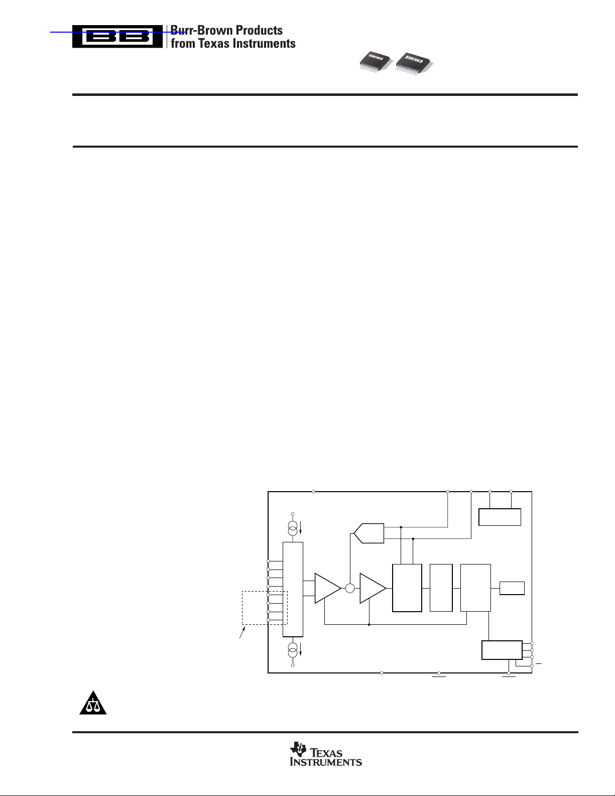
DESCRIPTION
The ADS1242 and ADS1243 are precision, wide dynamic
range, delta-sigma, analog-to-digital (A/D) converters with
24-bit resolution operating from 2.7V to 5.25V supplies.
These delta-sigma, A/D converters provide up to 24 bits of no
missing code performance and effective resolution of 21 bits.
The input channels are multiplexed. Internal buffering can be
selected to provide a very high input impedance for direct
connection to transducers or low-level voltage signals. Burnout current sources are provided that allow for the detection
of an open or shorted sensor. An 8-bit digital-to-analog
converter (DAC) pr o vides an offset correction with a range of
50% of the FSR (Full-Scale Range).
The Programmable Gain Amplifier (PGA) provides selectable
gains of 1 to 128 with an effective resolution of 19 bits at a gain
of 128. The A/D conversion is accomplished with a second-order
delta-sigma modulator and programmable FIR filter that provides a simultaneous 50Hz and 60Hz notch. The reference input
is differential and can be used for ratiometric conversion.
The serial interface is SPI compatible. Up to eight bits of data
I/O are also provided that can be used for input or output. The
ADS1242 and ADS1243 are designed for high-resolution
measurement applications in smart transmitters, industrial
process control, weight scales, chromatography, and portable
instrumentation.
V
DD
Offset
DAC
V
REF+VREF–
X
X
IN
OUT
Clock Generator
0/D0
A
IN
1/D1
A
IN
A
2/D2
IN
3/D3
A
IN
4/D4
A
IN
5/D5
A
IN
6/D6
A
IN
A
7/D7
IN
ADS1243
Only
Please be aware that an important notice concerning availability, standard warranty, and use in critical applications of
Texas Instruments semiconductor products and disclaimers thereto appears at the end of this data sheet.
All trademarks are the property of their respective owners.
PRODUCTION DATA information is current as of publication date.
Products conform to specifications per the terms of Texas Instruments
standard warranty. Production processing does not necessarily include
testing of all parameters.
IN+
MUX
IN–
2µA
GND
www.ti.com
A = 1:128
+
BUF PGA
GND
2nd-Order
Modulator
Digital
PDWN DRDY
Filter
Controller Registers
Serial Interface
Copyright © 2001-2004, Texas Instruments Incorporated
SCLK
D
IN
D
OUT
CS
ABSOLUTE MAXIMUM RATINGS
VDD to GND ........................................................................... –0.3V to +6V
Input Current ............................................................... 100mA, Momentary
Input Current .................................................................10mA, Continuous
A
.................................................................... GND – 0.5V to VDD + 0.5V
IN
Digital Input Voltage to GND...................................... –0.3V to V
Digital Output Voltage to GND ................................... –0.3V to V
Maximum Junction Temperature ................................................... +150°C
Operating Temperature Range ......................................... –40°C to +85°C
Storage Temperature Range .......................................... –60°C to +100°C
Lead Temperature (soldering, 10s) .............................................. +300°C
NOTE: (1) Stresses above those listed under “Absolute Maximum Ratings” may
cause permanent damage to the device. Exposure to absolute maximum
conditions for extended periods may affect device reliability.
(1)
+ 0.3V
DD
+ 0.3V
DD
DEMO BOARD ORDERING INFORMATION
PRODUCT DESCRIPTION
ADS1241-EVM ADS1241 Evaluation Module
ELECTROSTATIC
DISCHARGE SENSITIVITY
This integrated circuit can be damaged by ESD. Texas Instruments recommends that all integrated circuits be handled with
appropriate precautions. Failure to observe proper handling
and installation procedures can cause damage.
ESD damage can range from subtle performance degradation
to complete device failure. Precision integrated circuits may be
more susceptible to damage because very small parametric
changes could cause the device not to meet its published
specifications.
PACKAGE/ORDERING INFORMATION
PRODUCT PACKAGE-LEAD DESIGNATOR RANGE MARKING NUMBER
ADS1242 TSSOP-16 PW –40°C to +85°C ADS1242 ADS1242IPWT Tape and Reel, 250
(1)
PACKAGE TEMPERATURE PACKAGE ORDERING TRANSPORT
SPECIFIED
(2)
MEDIA, QUANTITY
" """"ADS1242IPWR Tape and Reel, 2500
ADS1243 TSSOP-20 PW –40°C to +85°C ADS1243 ADS1243IPWT Tape and Reel, 250
" """"ADS1243IPWR Tape and Reel, 2500
NOTES: (1) For the most current package and ordering information, see the Package Option Addendum located at the end of this data sheet.
(2) The ordering number contains grade, temperature range, package, and transport media information. Ordering the ADS1242IPWT will get a single
250-piece tape and reel of the ADS1242, Industrial Temperature Range device in a PW package.
DIGITAL CHARACTERISTICS: T
PARAMETER CONDITIONS MIN TYP MAX UNITS
Digital Input/Output
Logic Family CMOS
Logic Level: V
Input Leakage: I
Master Clock Rate: f
Master Clock Period: t
NOTE: (1) V
IH
(1)
V
IL
V
OH
V
OL
IH
I
IL
OSC
OSC
for XIN is GND to GND + 0.05V.
IL
MIN
to T
, VDD 2.7V to 5.25V
MAX
0.8 • V
DD
IOH = 1mA VDD – 0.4 V
IOL = 1mA GND GND + 0.4 V
VI = V
DD
VI = 0 –10 µA
1/f
OSC
GND 0.2 • V
15MHz
200 1000 ns
V
DD
10 µA
V
DD
V
2
www.ti.com
ADS1242, 1243
SBAS235B
ELECTRICAL CHARACTERISTICS: VDD = 5V
All specifications T
PARAMETER CONDITIONS MIN TYP MAX UNITS
ANALOG INPUT
Analog Input Range Buffer OFF GND – 0.1 V
Full-Scale Input Range
Differential Input Impedance Buffer OFF 5/PGA MΩ
Bandwidth
f
= 3.75Hz –3dB 1.65 Hz
DATA
f
= 7.50Hz –3dB 3.44 Hz
DATA
f
= 15.00Hz –3dB 14.6 Hz
DATA
Programmable Gain Amplifier User-Selectable Gain Ranges 1 128
Input Capacitance 9pF
Input Leakage Current Modulator OFF, T = 25°C5 pA
Burnout Current Sources 2 µA
OFFSET DAC
Offset DAC Range RANGE = 0 ±V
Offset DAC Monotonicity 8 Bits
Offset DAC Gain Error ±10 %
Offset DAC Gain Error Drift 1 ppm/°C
SYSTEM PERFORMANCE
Resolution No Missing Codes 24 Bits
Integral Nonlinearity End Point Fit ±0.0015 % of FS
Offset Error
Offset Drift
Gain Error
Gain Error Drift
Common-Mode Rejection at DC 100 dB
Normal-Mode Rejection f
Output Noise See Typical Characteristics
Power-Supply Rejection at DC, dB = –20 log(∆V
VOLTAGE REFERENCE INPUT
Reference Input Range REF IN+, REF IN– 0V
V
REF
Common-Mode Rejection at DC 120 dB
Common-Mode Rejection f
Bias Current
POWER-SUPPLY REQUIREMENTS
Power-Supply Voltage V
Current PGA = 1, Buffer OFF 240 375 µA
Power Dissipation PGA = 1, Buffer OFF 1.2 1.9 mW
TEMPERATURE RANGE
Operating –40 +85 °C
Storage –60 +100 °C
NOTES: (1) Calibration can minimize these errors. (2) ∆V
(1)
(1)
(1)
(3)
to T
MIN
(AIN0 – AIN7)
(1)
, VDD = +5V, f
MAX
= 19.2kHz, PGA = 1, Buffer ON, f
MOD
DATA
Buffer ON GND + 0.05 V
(In+) – (In–), See Block Diagram, RANGE = 0
RANGE = 1
Buffer ON 5 GΩ
RANGE = 1 ±V
f
= 60Hz, f
CM
f
= 50Hz, f
CM
= 50Hz, f
SIG
f
= 60Hz, f
SIG
V
≡ (REF IN+) – (REF IN–), RANGE = 0
REF
RANGE = 1 0.1 V
= 60Hz, f
VREFCM
V
REF
= 15Hz 130 dB
DATA
= 15Hz 120 dB
DATA
= 15Hz 100 dB
DATA
= 15Hz 100 dB
DATA
(2)
)
OUT/VDD
= 15Hz 120 dB
DATA
= 2.5V 1.3 µA
DD
PGA = 128, Buffer OFF 450 800 µA
PGA = 1, Buffer ON 290 425 µA
PGA = 128, Buffer ON 960 1400 µA
SLEEP Mode 60 µA
Read Data Continuous Mode
PDWN 0.5 nA
is a change in digital result. (3) 12pF switched capacitor at f
OUT
= 15Hz, V
≡ (REF IN+) – (REF IN–) = +2.5V, unless otherwise specified.
REF
ADS1242
ADS1243
+ 0.1 V
DD
– 1.5 V
DD
±V
REF
±V
/(2 • PGA)
REF
/(2 • PGA) V
REF
/(4 • PGA) V
REF
7.5 ppm of FS
0.02 ppm of FS/°C
0.005 %
0.5 ppm/°C
80 95 dB
0.1 2.5 2.6 V
DD
DD
4.75 5.25 V
230 µA
clock frequency.
SAMP
/PGA V
V
V
V
ADS1242, 1243
SBAS235B
www.ti.com
3

ELECTRICAL CHARACTERISTICS: VDD = 3V
All specifications T
PARAMETER CONDITIONS MIN TYP MAX UNITS
ANALOG INPUT
Analog Input Range Buffer OFF GND – 0.1 V
Full-Scale Input Voltage Range
Input Impedance Buffer OFF 5/PGA MΩ
Bandwidth
f
= 3.75Hz –3dB 1.65 Hz
DATA
f
= 7.50Hz –3dB 3.44 Hz
DATA
f
= 15.00Hz –3dB 14.6 Hz
DATA
Programmable Gain Amplifier User-Selectable Gain Ranges 1 128
Input Capacitance 9pF
Input Leakage Current Modulator OFF, T = 25°C5 pA
Burnout Current Sources 2 µA
OFFSET DAC
Offset DAC Range RANGE = 0 ±V
Offset DAC Monotonicity 8 Bits
Offset DAC Gain Error ±10 %
Offset DAC Gain Error Drift 2 ppm/°C
SYSTEM PERFORMANCE
Resolution No Missing Codes 24 Bits
Integral Nonlinearity End Point Fit ±0.0015 % of FS
Offset Error
Offset Drift
Gain Error
Gain Error Drift
Common-Mode Rejection at DC 100 dB
Normal-Mode Rejection f
Output Noise See Typical Characteristics
Power-Supply Rejection at DC, dB = –20 log(∆V
VOLTAGE REFERENCE INPUT
Reference Input Range REF IN+, REF IN– 0V
V
REF
Common-Mode Rejection at DC 120 dB
Common-Mode Rejection f
Bias Current
POWER-SUPPLY REQUIREMENTS
Power-Supply Voltage V
Current PGA = 1, Buffer OFF 190 375 µA
Power Dissipation PGA = 1, Buffer OFF 0.6 1.2 mW
TEMPERATURE RANGE
Operating –40 +85 °C
Storage –60 +100 °C
NOTES: (1) Calibration can minimize these errors. (2) ∆V
(1)
(1)
(1)
(3)
to T
MIN
(AIN0 – AIN7)
(1)
, VDD = +3V, f
MAX
= 19.2kHz, PGA = 1, Buffer ON, f
MOD
DATA
Buffer ON GND + 0.05 V
(In+) – (In–) See Block Diagram, RANGE = 0
RANGE = 1
Buffer ON 5 GΩ
RANGE = 1 ±V
f
= 60Hz, f
CM
f
= 50Hz, f
CM
= 50Hz, f
SIG
f
= 60Hz, f
SIG
V
≡ (REF IN+) – (REF IN–), RANGE = 0
REF
RANGE = 1 0.1 2.5 2.6 V
= 60Hz, f
VREFCM
V
REF
= 15Hz 130 dB
DATA
= 15Hz 120 dB
DATA
= 15Hz 100 dB
DATA
= 15Hz 100 dB
DATA
(2)
)
OUT/VDD
= 15Hz 120 dB
DATA
= 1.25 0.65 µA
DD
PGA = 128, Buffer OFF 460 700 µA
PGA = 1, Buffer ON 240 375 µA
PGA = 128, Buffer ON 870 1325 µA
SLEEP Mode 75 µA
Read Data Continuous Mode
PDWN = 0 0.5 nA
is a change in digital result. (3) 12pF switched capacitor at f
OUT
= 15Hz, V
≡ (REF IN+) – (REF IN–) = +1.25V, unless otherwise specified.
REF
ADS1242
ADS1243
+ 0.1 V
DD
– 1.5 V
DD
±V
/PGA V
REF
±V
/(2 • PGA)
REF
/(2 • PGA) V
REF
/(4 • PGA) V
REF
15 ppm of FS
0.04 ppm of FS/°C
0.01 %
1.0 ppm/°C
75 90 dB
0.1 1.25 1.30 V
DD
2.7 3.3 V
113 µA
clock frequency.
SAMP
V
V
4
www.ti.com
ADS1242, 1243
SBAS235B
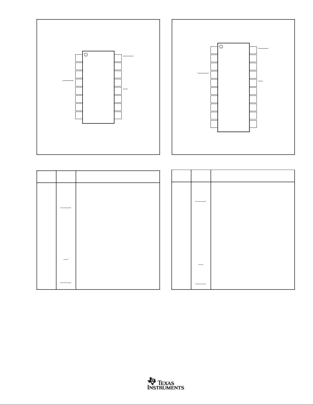
PIN CONFIGURATION (ADS1242)
PIN CONFIGURATION (ADS1243)
Top View TSSOP Top View TSSOP
V
X
X
OUT
PDWN
V
REF+
V
REF–
AIN0/D0
A
1/D1
IN
1
DD
2
IN
3
4
ADS1242
5
6
7
8
16
DRDY
15
SCLK
14
D
OUT
13
D
IN
12
CS
11
GND
10
A
3/D3
IN
9
A
2/D2
IN
PIN DESCRIPTIONS (ADS1242)
PIN
NUMBER NAME DESCRIPTION
1V
2X
3X
4 PDWN Active LOW. Power Down. The power down func-
5V
6V
7A
8A
9A
10 A
REF+
REF–
IN
IN
IN
IN
11 GND Ground
12 CS Active LOW, Chip Select
13 D
14 D
15 SCLK Serial Clock, Schmitt Trigger
16 DRDY Active LOW, Data Ready
Power Supply
DD
Clock Input
IN
Clock Output, used with crystal or ceramic
OUT
resonator.
tion shuts down the analog and digital circuits.
Positive Differential Reference Input
Negative Differential Reference Input
0/D0 Analog Input 0/Data I/O 0
1/D1 Analog Input 1/Data I/O 1
2/D2 Analog Input 2/Data I/O 2
3/D3 Analog Input 3/Data I/O 3
Serial Data Input, Schmitt Trigger
IN
Serial Data Output
OUT
V
X
X
OUT
PDWN
V
REF+
V
REF–
AIN0/D0
A
1/D1
IN
A
4/D4
IN
A
5/D5
IN
1
DD
2
IN
3
4
5
ADS1243
6
7
8
9
10
20
DRDY
19
SCLK
18
D
OUT
17
D
IN
16
CS
15
GND
14
A
3/D3
IN
13
A
2/D2
IN
12
A
7/D7
IN
11
A
6/D6
IN
PIN DESCRIPTIONS (ADS1243)
PIN
NUMBER NAME DESCRIPTION
1V
2X
3X
OUT
4 PDWN Active LOW. Power Down. The power down func-
5V
6V
7A
8A
9A
10 A
11 A
12 A
13 A
14 A
15 GND Ground
REF+
REF–
IN
IN
IN
IN
IN
IN
IN
IN
16 CS Active LOW, Chip Select
17 D
18 D
19 SCLK Serial Clock, Schmitt Trigger
20 DRDY Active LOW, Data Ready
Power Supply
DD
Clock Input
IN
Clock Output, used with crystal or ceramic
resonator.
tion shuts down the analog and digital circuits.
Positive Differential Reference Input
Negative Differential Reference Input
0/D0 Analog Input 0/Data I/O 0
1/D1 Analog Input 1/Data I/O 1
4/D4 Analog Input 4/Data I/O 4
5/D5 Analog Input 5/Data I/O 5
6/D6 Analog Input 6/Data I/O 6
7/D7 Analog Input 7/Data I/O 7
2/D2 Analog Input 2/Data I/O 2
3/D3 Analog Input 3/Data I/O 3
Serial Data Input, Schmitt Trigger
IN
Serial Data Output
OUT
ADS1242, 1243
SBAS235B
www.ti.com
5
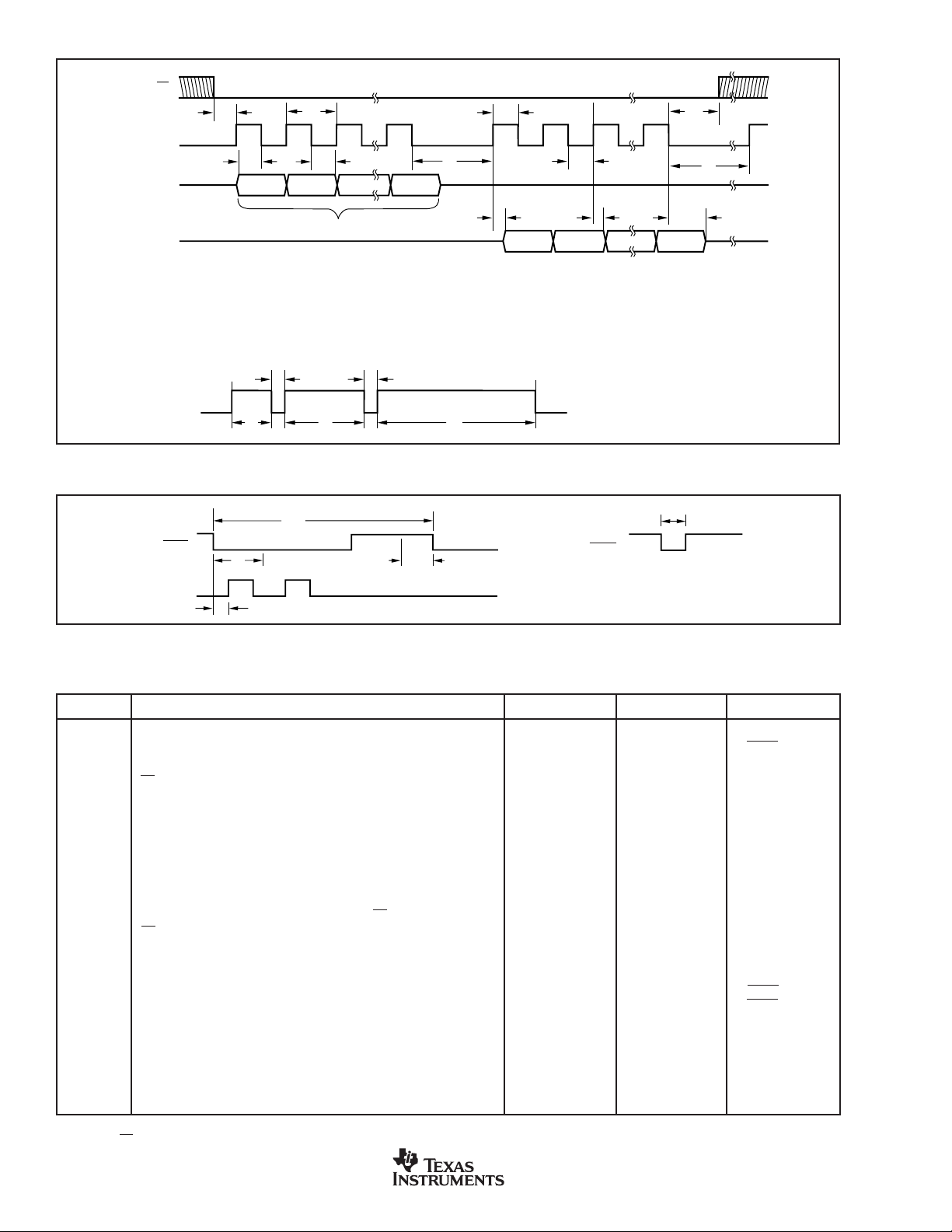
TIMING DIAGRAMS
CS
SCLK
(POL = 0)
D
IN
t
3
t
4
MSB
t
1
t
5
t
2
t
6
t
2
t
10
t
11
LSB
DIAGRAM 1.
DIAGRAM 2.
D
OUT
NOTE: (1) Bit order = 0.
SCLK Reset Waveform
SCLK
DRDY
SCLK
(Command or Command and Data)
t
13
t
12
t
17
t
19
t
DATA
t
14
t
7
MSB
t
8
(1)
LSB
t
9
(1)
ADS1242 or ADS1243
Resets On
t
Falling Edge
13
t
15
t
18
300 • t
t13 : > 5 • t
550 • t
1050 • t
PDWN
< t12 < 500 • t
OSC
OSC
< t14 < 750 • t
OSC
< t15 < 1250 • t
OSC
OSC
OSC
OSC
t
16
TIMING CHARACTERISTICS TABLES
SPEC DESCRIPTION MIN MAX UNITS
t
1
t
2
t
3
t
4
t
5
t
6
(1)
t
7
(1)
t
8
t
9
t
10
t
11
t
16
t
17
t
18
t
19
NOTES: (1) Load = 20pF 10kΩ to GND.
SCLK Period 4t
3 DRDY Periods
SCLK Pulse Width, HIGH and LOW 200 ns
CS low to first SCLK Edge; Setup Time
(2)
0ns
DIN Valid to SCLK Edge; Setup Time 50 ns
Valid DIN to SCLK Edge; Hold Time 50 ns
Delay between last SCLK edge for DIN and first SCLK edge for D
OUT
:
RDATA, RDATAC, RREG, WREG 50 t
SCLK Edge to Valid New D
SCLK Edge to D
Last SCLK Edge to D
NOTE: D
OUT
, Hold Time 0 ns
OUT
Tri-State 6 10 t
OUT
goes tri-state immediately when CS goes HIGH.
OUT
50 ns
CS LOW time after final SCLK edge. 0 ns
Final SCLK edge of one command until first edge SCLK
of next command:
RREG, WREG, DSYNC, SLEEP, RDATA, RDATAC, STOPC
4t
SELFGCAL, SELFOCAL, SYSOCAL, SYSGCAL 2 DRDY Periods
SELFCAL 4 DRDY Periods
RESET (also SCLK Reset) 16 t
Pulse Width 4t
Allowed analog input change for next valid conversion. 5000 t
DOR update, DOR data not valid. 4 t
First SCLK after DRDY goes LOW:
RDATAC Mode 10 t
Any other mode 0 t
(2) CS may be tied LOW.
OSC
OSC
OSC
OSC
OSC
OSC
OSC
OSC
OSC
OSC
Periods
Periods
Periods
Periods
Periods
Periods
Periods
Periods
Periods
Periods
6
www.ti.com
ADS1242, 1243
SBAS235B
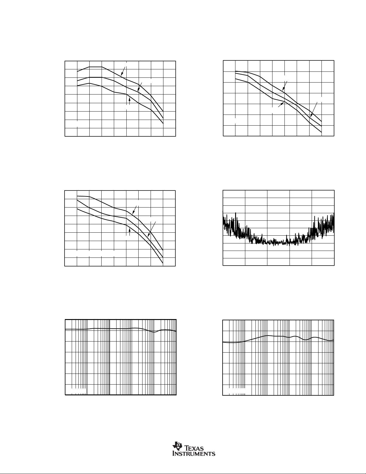
TYPICAL CHARACTERISTICS
POWER SUPPLY REJECTION RATIO
vs FREQUENCY
Frequency of Power Supply (Hz)
110 1k100 10k 100k
PSRR (dB)
140
120
100
80
60
40
20
0
Buffer ON
All specifications, VDD = +5V, f
= 2.4576MHz, PGA = 1, f
OSC
= 15Hz, and V
DATA
≡ (REF IN+) – (REF IN–) = +2.5V, unless otherwise specified.
REF
21.5
21.0
20.5
20.0
19.5
19.0
ENOB (rms)
18.5
18.0
Buffer OFF
17.5
17.0
20.5
20.0
19.5
19.0
18.5
18.0
ENOB (rms)
17.5
17.0
16.5
16.0
EFFECTIVE NUMBER OF BITS vs PGA SETTING
DR = 10
DR = 01
DR = 00
1 2 4 8 16 1286432
PGA Setting
EFFECTIVE NUMBER OF BITS vs PGA SETTING
DR = 10
DR = 01
DR = 00
Buffer OFF, V
1 2 4 8 16 64 12832
REF
= 1.25V
PGA Setting
EFFECTIVE NUMBER OF BITS vs PGA SETTING
22
21
DR = 00
PGA Setting
V
IN
DR = 10
DR = 01
(V)
20
19
18
ENOB (rms)
17
Buffer ON
16
15
2.0
1.8
1.6
1.4
1.2
1.0
0.8
0.6
Noise (rms, ppm of FS)
0.4
0.2
1 2 4 8 16 1286432
NOISE vs INPUT SIGNAL
0
–2.5 –1.5 0.5–0.5 1.5 2.5
COMMON-MODE REJECTION RATIO
140
120
100
80
60
CMRR (dB)
40
20
Buffer ON
0
1 10 100 1k 10k 100k
Frequency of Power Supply (Hz)
ADS1242, 1243
SBAS235B
vs FREQUENCY
www.ti.com
7
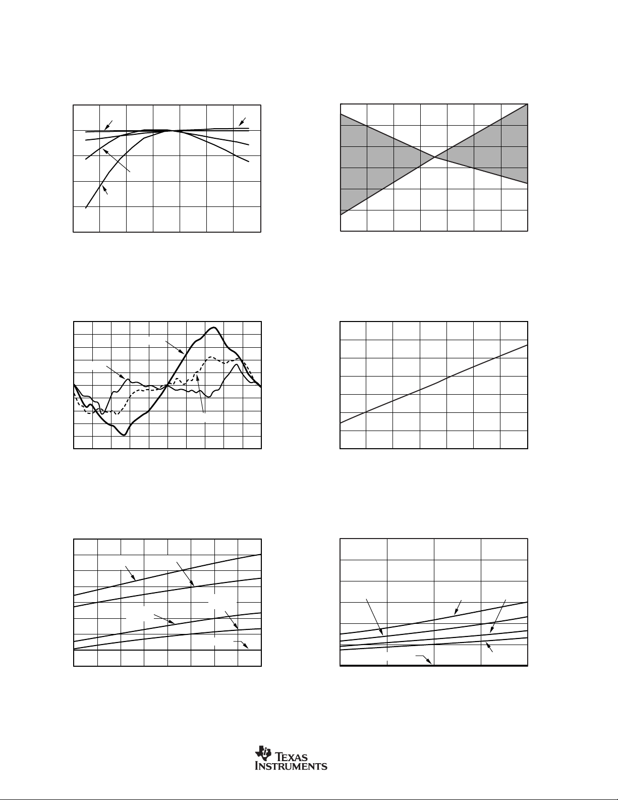
TYPICAL CHARACTERISTICS (Cont.)
All specifications, VDD = +5V, f
= 2.4576MHz, PGA = 1, f
OSC
= 15Hz, and V
DATA
≡ (REF IN+) – (REF IN–) = +2.5V, unless otherwise specified.
REF
OFFSET vs TEMPERATURE
50
PGA1
0
–50
–100
Offset (ppm of FS)
–150
–200
–50 –30 10–10 30 50 70 90
10
8
6
4
2
0
–2
INL (ppm of FS)
–4
–6
–8
–10
–2.5 –2.0 –1.0 –0.5–1.5 0 0.5 1.0 1.5 2.0 2.5
PGA128
INTEGRAL NONLINEARITY vs INPUT SIGNAL
+85°C
(Cal at 25°C)
PGA64
Temperature (°C)
–40°C
V
(V)
IN
+25°C
PGA16
1.00010
1.00006
1.00002
0.99998
0.99994
Gain (Normalized)
0.99990
0.99986
–50 –30 10–10 30 50 70 90
260
250
240
230
220
Current (µA)
210
200
190
–50 –30 10–10 30 50 70 90
GAIN vs TEMPERATURE
(Cal at 25°C)
Temperature (°C)
CURRENT vs TEMPERATURE
(Buffer Off)
Temperature (°C)
350
300
250
200
150
Current (µA)
100
50
0
–50
3.0 3.25 3.5 3.75 4.0 4.25 4.5 4.75 5.0
8
CURRENT vs VOLTAGE
Normal
4.91MHz
SLEEP
4.91MHz
Normal
2.45MHz
(V)
V
DD
SLEEP
2.45MHz
Power Down
www.ti.com
300
250
200
(µA)
DIGITAL
I
4.91MHz
150
100
50
0
3.0 3.5 4.0 4.5 5.0
SUPPLY CURRENT vs SUPPLY
SLEEP
Power Down
Normal
4.91MHz
(V)
V
DD
Normal
2.45MHz
SLEEP
2.45MHz
ADS1242, 1243
SBAS235B

TYPICAL CHARACTERISTICS (Cont.)
All specifications, VDD = +5V, f
3500
10k Readings
V
= 0V
500
0
IN
–3.5 –3.0
–2.5 –2.0 –1.5 –1 –0.5 0 0.5 1.0 1.5 2.0 2.5 3.0 3.5
3000
2500
2000
1500
1000
Number of Occurrences
= 2.4576MHz, PGA = 1, f
OSC
NOISE HISTOGRAM
ppm of FS
= 15Hz, and V
DATA
≡ (REF IN+) – (REF IN–) = +2.5V, unless otherwise specified.
REF
OFFSET DAC
OFFSET vs TEMPERATURE
200
170
140
110
80
50
20
–10
Offset (ppm of FSR)
–40
–70
–100
–50 –30 10–10 30 50 70 90
(Cal at 25°C)
Temperature (°C)
1.00020
1.00016
1.00012
1.00008
1.00004
1.00000
0.99996
0.99992
Gain (Normalized)
0.99988
0.99984
0.99980
0.99976
–50 –30 10–10 30 50 70 90
OFFSET DAC
GAIN vs TEMPERATURE
(Cal at 25°C)
Temperature (°C)
OFFSET DAC
0.8
0.7
0.6
0.5
0.4
0.3
0.2
Noise (rms, ppm of FS)
0.1
0
–128 –96 –64 –320 326496128
NOISE vs SETTING
Offset DAC Setting
ADS1242, 1243
SBAS235B
www.ti.com
9

OVERVIEW
INPUT MULTIPLEXER
The input multiplexer provides for any combination of differential inputs to be selected on any of the input channels, as
shown in Figure 1. For example, if A
positive differential input channel, any other channel can be
selected as the negative terminal for the differential input
A
0/D0
IN
A
1/D1
IN
2/D2
A
IN
0 is selected as the
IN
V
DD
Burnout Current Source
channel. With this method, it is possible to have up to eight
single-ended input channels or four independent differential
input channels for the ADS1243, and four single-ended input
channels or two independent differential input channels for
the ADS1242. Note that A
can be treated as an input
INCOM
channel.
The ADS1242 and ADS1243 feature a single-cycle settling
digital filter that provides valid data on the first conversion
after a new channel selection. In order to minimize the
settling error, synchronize MUX changes to the conversion
beginning, which is indicated by the falling edge of
DRDY
. In
other words, issuing a MUX change through the WREG
command immediately after
DRDY
goes LOW minimizes the
settling error. Increasing the time between the conversion
beginning (
mand (t
DRDY
goes LOW) and the MUX change com-
) results in a settling error in the conversion
DELAY
data, as shown in Figure 2.
AIN3/D3
4/D4
A
IN
5/D5
A
IN
6/D6
A
ADS1243
Only
IN
7/D7
A
IN
A
INCOM
GND
FIGURE 1. Input Multiplexer Configuration.
New Conversion Begins,
Complete Previous Conversion
DRDY
SCLK
(POL = 0)
Input
Buffer
Burnout Current Source
t
DELAY
Previous Conversion Data
BURNOUT CURRENT SOURCES
The Burnout Current Sources can be used to detect sensor
short-circuit or open-circuit conditions. Setting the Burnout
Current Sources (BOCS) bit in the SETUP register activates
two 2µA current sources called burnout current sources. One
of the current sources is connected to the converter’s negative input and the other is connected to the converter’s
positive input.
Figure 3 shows the situation for an open-circuit sensor. This
is a potential failure mode for many kinds of remotely connected sensors. The current source on the positive input acts
as a pull-up, causing the positive input to go to the positive
analog supply, and the current source on the negative input
acts as a pull-down, causing the negative input to go to
ground. The ADS1242/43 therefore outputs full-scale (7FFFFF
Hex).
New Conversion Complete
DIN
FIGURE 2. Input Multiplexer Configuration.
10
MSB LSB
SETTLING ERROR vs DELAY TIME
10.000000
1.000000
0.100000
0.010000
0.001000
Settling Error (%)
0.000100
0.000010
0.000001
2 4 6 8 10 12 14 160
f
= 2.4576MHz
CLK
Delay Time, t
www.ti.com
DELAY
(ms)
ADS1242, 1243
SBAS235B

V
DD
2µA
V
DD
0V
ADC
CODE = 0x7FFFFF
H
OPEN CIRCUIT
2µA
FIGURE 3. Burnout detection while sensor is open-circuited.
Figure 4 shows a short-circuited sensor. Since the inputs are
shorted and at the same potential, the ADS1242/43 signal
outputs are approximately zero. (Note that the code for
shorted inputs is not exactly zero due to internal series
resistance, low-level noise and other error sources.)
V
DD
The buffer draws additional current when activated. The
current required by the buffer depends on the PGA setting.
When the PGA is set to 1, the buffer uses approximately
50µA; when the PGA is set to 128, the buffer uses approxi-
mately 500µA.
PGA
The Programmable Gain Amplifier (PGA) can be set to gains
of 1, 2, 4, 8, 16, 32, 64, or 128. Using the PGA can improve the
effective resolution of the A/D converter. For instance, with a
PGA of 1 on a 5V full-scale signal, the A/D converter can
resolve down to 1µV. With a PGA of 128 and a full-scale signal
of 39mV, the A/D converter can resolve down to 75nV. V
DD
current increases with PGA settings higher than 4.
OFFSET DAC
The input to the PGA can be shifted by half the full-scale input
range of the PGA using the Offset DAC (ODAC) register. The
ODAC register is an 8-bit value; the MSB is the sign and the
seven LSBs provide the magnitude of the offset. Using the
offset DAC does not reduce the performance of the A/D
converter. For more details on the ODAC in the ADS1242/43,
please refer to TI application report SBAA077 (available
through the TI website).
2µA
/2
V
DD
SHORT
CIRCUIT
V
2µA
ADC
/2
DD
CODE ≅ 0
FIGURE 4. Burnout detection while sensor is short-circuited.
INPUT BUFFER
The input impedance of the ADS1242/43 without the buffer
enabled is approximately 5MΩ/PGA. For systems requiring
very high input impedance, the ADS1242/43 provides a
chopper-stabilized differential FET-input voltage buffer. When
activated, the buffer raises the ADS1242/43 input impedance
to approximately 5GΩ.
The buffer’s input range is approximately 50mV to
V
– 1.5V. The buffer’s linearity will degrade beyond this
DD
range. Differential signals should be adjusted so that both
signals are within the buffer’s input range.
The buffer can be enabled using the BUFEN pin or the
BUFEN bit in the ACR register. The buffer is on when the
BUFEN pin is high and the BUFEN bit is set to one. If the
BUFEN pin is low, the buffer is disabled. If the BUFEN bit is
set to zero, the buffer is also disabled.
MODULATOR
The modulator is a single-loop second-order system. The
modulator runs at a clock speed (f
the external clock (f
). The frequency division is deter-
OSC
) that is derived from
MOD
mined by the SPEED bit in the SETUP register, as shown in
Table I.
f
OSC
2.4576MHz 0 19,200Hz 15Hz 7.5Hz 3.75Hz 50/60Hz
4.9152MHz 0 38,400Hz 30Hz 15Hz 7.5Hz 100/120Hz
SPEED DR BITS 1st NOTCH
BIT f
MOD
1 9,600Hz 7.5Hz 3.75Hz 1.875Hz 25/30Hz
1 19,200Hz 15Hz 7.5Hz 3.75Hz 50/60Hz
00 01 10 FREQ.
TABLE I. Output Configuration.
CALIBRATION
The offset and gain errors can be minimized with calibration.
The ADS1242 and ADS1243 support both self and system
calibration.
Self-calibration of the ADS1242 and ADS1243 corrects internal offset and gain errors and is handled by three commands:
SELFCAL, SELFGAL, and SELFOCAL. The SELFCAL command performs both an offset and gain calibration. SELFGCAL
performs a gain calibration and SELFOCAL performs an
offset calibration, each of which takes two t
complete. During self-calibration, the ADC inputs are disconnected internally from the input pins. The PGA must be set to
1 prior to issuing a SELFCAL or SELFGCAL command. Any
PGA is allowed when issuing a SELFOCAL command. For
periods to
DATA
ADS1242, 1243
SBAS235B
www.ti.com
11

C
1
Crystal
X
IN
X
OUT
C
2
example, if using PGA = 64, first set PGA = 1 and issue
SELFGCAL. Afterwards, set PGA = 64 and issue SELFOCAL.
For operation with a reference voltage greater than
(V
– 1.5) volts, the buffer must also be turned off during
DD
gain self-calibration to avoid exceeding the buffer input
range.
System calibration corrects both internal and external offset
and gain errors. While performing system calibration, the
appropriate signal must be applied to the inputs. The system
offset calibration command (SYSOCAL) requires a zero input
differential signal (see Table IV, page 18). It then computes
the offset that nullifies the offset in the system. The system
gain calibration command (SYSGCAL) requires a positive
full-scale input signal. It then computes a value to nullify the
gain error in the system. Each of these calibrations takes two
t
periods to complete. System gain calibration is recom-
DATA
mended for the best gain calibration at higher PGAs.
Calibration should be performed after power on, a change in
temperature, or a change of the PGA. The RANGE bit (ACR bit
2) must be zero during calibration.
Calibration removes the effects of the ODAC; therefore, dis-
able the ODAC during calibration, and enable again after
calibration is complete.
At the completion of calibration, the
DRDY
signal goes low,
indicating the calibration is finished. The first data after
calibration should be discarded since it may be corrupt from
calibration data remaining in the filter. The second data is
always valid.
EXTERNAL VOLTAGE REFERENCE
The ADS1242 and ADS1243 require an external voltage
reference. The selection for the voltage reference value is
made through the ACR register.
The external voltage reference is differential and is represented by the voltage difference between the pins: +V
and –V
–V
REF,
. The absolute voltage on either pin, +V
REF
can range from GND to VDD. However, the following
REF
REF
or
limitations apply:
For V
V
For V
V
For V
V
For V
V
= 5.0V and RANGE = 0 in the ACR, the differential
DD
must not exceed 2.5V.
REF
= 5.0V and RANGE = 1 in the ACR, the differential
DD
must not exceed 5V.
REF
= 3.0V and RANGE = 0 in the ACR, the differential
DD
must not exceed 1.25V.
REF
= 3.0V and RANGE = 1 in the ACR, the differential
DD
must not exceed 2.5V.
REF
CLOCK GENERATOR
The clock source for the ADS1242 and ADS1243 can be
provided from a crystal, oscillator, or external clock. When the
clock source is a crystal, external capacitors must be provided
to ensure start-up and stable clock frequency. This is shown in
both Figure 5 and Table II. X
crystals and it should not be used as a clock driver for external
circuitry.
12
is only for use with external
OUT
www.ti.com
FIGURE 5. Crystal Connection.
CLOCK PART
SOURCE FREQUENCY C
Crystal 2.4576 0-20pF 0-20pF ECS, ECSD 2.45 - 32
Crystal 4.9152 0-20pF 0-20pF ECS, ECSL 4.91
Crystal 4.9152 0-20pF 0-20pF ECS, ECSD 4.91
Crystal 4.9152 0-20pF 0-20pF CTS, MP 042 4M9182
C
1
2
NUMBER
TABLE II. Recommended Crystals.
DIGITAL FILTER
The ADS1242 and ADS1243 have a 1279 tap linear phase
Finite Impulse Response (FIR) digital filter that a user can
configure for various output data rates. When a 2.4576MHz
crystal is used, the device can be programmed for an output
data rate of 15Hz, 7.5Hz, or 3.75Hz. Under these conditions,
the digital filter rejects both 50Hz and 60Hz interference. Figure
6 shows the digital filter frequency response for data output
rates of 15Hz, 7.5Hz, and 3.75Hz.
If a different data output rate is desired, a different crystal
frequency can be used. However, the rejection frequencies
shift accordingly. For example, a 3.6864MHz master clock with
the default register condition has:
(3.6864MHz/2.4576MHz) • 15Hz = 22.5Hz data output rate
and the first and second notch is:
1.5 • (50Hz and 60Hz) = 75Hz and 90Hz
DATA I/O INTERFACE
The ADS1242 has four pins and the ADS1243 has eight pins
that serve a dual purpose as both analog inputs and data
I/O. These pins are configured through the IOCON, DIR, and
DIO registers and can be individually configured as either
analog inputs or data I/O. See Figure 7 (page 14) for the
equivalent schematic of an Analog/Data I/O pin.
The IOCON register defines the pin as either an analog input
or data I/O. The power-up state is an analog input. If the pin
is configured as an analog input in the IOCON register, the
DIR and DIO registers have no effect on the state of the pin.
If the pin is configured as data I/O in the IOCON register,
then DIR and DIO are used to control the state of the pin.
The DIR register controls the direction of the data pin, either
as an input or output. If the pin is configured as an input in
the DIR register, then the corresponding DIO register bit
reflects the state of the pin. Make sure the pin is driven to a
logic one or zero when configured as an input to prevent
ADS1242, 1243
SBAS235B

ADS1242 AND ADS1243
0
FILTER RESPONSE WHEN f
DATA
–20
–40
–60
–80
–100
Gain (dB)
–120
–140
–160
–180
020 8040 60 100 120 140 160 180 200
Frequency (Hz)
= 15Hz
FREQUENCY RESPONSE FROM 45Hz to 65Hz
–40
WHEN f
DATA
= 15Hz
–50
–60
–70
–80
–90
–100
Magnitude (dB)
–110
–120
–130
–140
45 50 55 60 65
Frequency (Hz)
ADS1242 AND ADS1243
0
FILTER RESPONSE WHEN f
DATA
–20
–40
–60
–80
–100
Gain (dB)
–120
–140
–160
–180
020 8040 60 100 120 140 160 180 200
Frequency (Hz)
ADS1242 AND ADS1243
0
FILTER RESPONSE WHEN f
DATA
= 3.75Hz
–20
–40
–60
–80
–100
Gain (dB)
–120
–140
–160
–180
020 8040 60 100 120 140 160 180 200
Frequency (Hz)
= 7.5Hz
FREQUENCY RESPONSE FROM 45Hz to 65Hz
–40
WHEN f
DATA
= 7.5Hz
–50
–60
–70
–80
–90
–100
Magnitude (dB)
–110
–120
–130
–140
45 50 55 60 65
Frequency (Hz)
FREQUENCY RESPONSE FROM 45Hz to 65Hz
–40
WHEN f
DATA
= 3.75Hz
–50
–60
–70
–80
–90
–100
Magnitude (dB)
–110
–120
–130
–140
45 50 55 60 65
Frequency (Hz)
f
OSC
DATA –3dB
OUTPUT RATE BANDWIDTH f
15Hz 14.6Hz –80.8dB –87.3dB –68.5dB –76.1dB
7.5Hz 3.44Hz –85.9dB –87.4dB –71.5dB –76.2dB
3.75Hz 1.65Hz –93.8dB –88.6dB –86.8dB –77.3dB
FIGURE 6. Filter Frequency Responses.
ADS1242, 1243
SBAS235B
= 2.4576MHz, SPEED = 0 or f
= 4.9152MHz, SPEED = 1
OSC
ATTENUATION
= 50 ± 0.3Hz fIN = 60 ± 0.3Hz fIN = 50 ± 1Hz fIN = 60 ± 1Hz
IN
www.ti.com
13

excess current dissipation. If the pin is configured as an
output in the DIR register, then the corresponding DIO
register bit value determines the state of the output pin
(0 = GND, 1 = V
DD
).
It is still possible to perform A/D conversions on a pin
configured as data I/O. This may be useful as a test mode,
where the data I/O pin is driven and an A/D conversion is
done on the pin.
IOCON
DIR
DIO WRITE
AINx/Dx
T o Analog Mux
DIO READ
FIGURE 7. Analog/Data Interface Pin.
SERIAL PERIPHERAL INTERFACE
The Serial Peripheral Interface (SPI) allows a controller to
communicate synchronously with the ADS1242 and ADS1243.
The ADS1242 and ADS1243 operate in slave-only mode.
The serial interface is a standard four-wire SPI (
D
and D
IN
) interface.
OUT
CS
, SCLK,
Chip Select (CS)
The chip select (CS) input must be externally asserted
before communicating with the ADS1242 or ADS1243.
CS
must stay LOW for the duration of the communication.
Whenever
CS
goes HIGH, the serial interface is reset.
CS
may be hard-wired LOW.
Serial Clock (SCLK)
The serial clock (SCLK) features a Schmitt-triggered input
and is used to clock D
a clean SCLK to prevent accidental double-shifting of the
data. If SCLK is not toggled within three
and D
IN
data. Make sure to have
OUT
DRDY
pulses, the
serial interface resets on the next SCLK pulse and starts a
new communication cycle. A special pattern on SCLK resets
the entire chip; see the RESET section for additional information.
Data Input (DIN) and Data Output (D
The data input (DIN) and data output (D
data from the ADS1242 and ADS1243. D
ance when not in use to allow D
and D
IN
OUT
)
OUT
) receive and send
is high imped-
OUT
to be connected
OUT
together and driven by a bidirectional bus. Note: the Read
Data Continuous Mode (RDATAC) command should not be
issued when D
mode, D
either of these 8-bit bytes appear on D
nected to D
DATA READY (
The
DRDY
and D
IN
looks for the STOPC or RESET command. If
IN
), the RDATAC mode ends.
IN
DRDY
are connected. While in RDATAC
OUT
(which is con-
OUT
) PIN
line is used as a status signal to indicate when
data is ready to be read from the internal data register.
DRDY
goes LOW when a new data word is available in the
DOR register. It is reset HIGH when a read operation from
the data register is complete. It also goes HIGH prior to the
updating of the output register to indicate when not to read
from the device to ensure that a data read is not attempted
while the register is being updated.
The status of
7 of the ACR register (address 2
operate in 3-wire mode by tying the
case, the SCLK, D
DRDY
can also be obtained by interrogating bit
). The serial interface can
H
CS
input LOW. In this
, and D
IN
lines are used to communi-
OUT
cate with the ADS1242 and ADS1243. This scheme is
suitable for interfacing to microcontrollers. If
CS
is required
as a decoding signal, it can be generated from a port bit of
the microcontroller.
POWER-UP—SUPPLY VOLTAGE RAMP RATE
The power-on reset circuitry was designed to accommodate
digital supply ramp rates as slow as 1V/10ms. To ensure
proper operation, the power supply should ramp monotonically.
14
www.ti.com
ADS1242, 1243
SBAS235B

ADS1242 AND ADS1243
REGISTERS
The operation of the device is set up through individual
registers. Collectively, the registers contain all the informa-
multiplexer settings, calibration settings, data rate, etc. The
16 registers are shown in Table III.
tion needed to configure the part, such as data format,
ADDRESS REGISTER BIT 7 BIT 6 BIT 5 BIT 4 BIT 3 BIT 2 BIT 1 BIT 0
00
01
02
03
04
05
06
07
08
09
0A
0B
0C
0D
0E
0F
H
H
H
H
H
H
H
H
H
H
H
H
H
H
H
H
SETUP ID ID ID ID BOCS PGA2 PGA1 PGA0
MUX PSEL3 PSEL2 PSEL1 PSEL0 NSEL3 NSEL2 NSEL1 NSEL0
ACR DRDY U/B SPEED BUFEN BIT ORDER RANGE DR1 DR0
ODAC SIGN OSET6 OSET5 OSET4 OSET3 OSET2 OSET1 OSET0
DIO DIO_7 DIO_6 DIO_5 DIO_4 DIO_3 DIO_2 DIO_1 DIO_0
DIR DIR_7 DIR_6 DIR_5 DIR_4 DIR_3 DIR_2 DIR_1 DIR_0
IOCON IO7 IO6 IO5 IO4 IO3 IO2 IO1 IO0
OCR0 OCR07 OCR06 OCR05 OCR04 OCR03 OCR02 OCR01 OCR00
OCR1 OCR15 OCR14 OCR13 OCR12 OCR11 OCR10 OCR09 OCR08
OCR2 OCR23 OCR22 OCR21 OCR20 OCR19 OCR18 OCR17 OCR16
FSR0 FSR07 FSR06 FSR05 FSR04 FSR03 FSR02 FSR01 FSR00
FSR1 FSR15 FSR14 FSR13 FSR12 FSR11 FSR10 FSR09 FSR08
FSR2 FSR23 FSR22 FSR21 FSR20 FSR19 FSR18 FSR17 FSR16
DOR2 DOR23 DOR22 DOR21 DOR20 DOR19 DOR18 DOR17 DOR16
DOR1 DOR15 DOR14 DOR13 DOR12 DOR11 DOR10 DOR09 DOR08
DOR0 DOR07 DOR16 FSR21 DOR04 DOR03 DOR02 DOR01 DOR00
TABLE III. Registers.
DETAILED REGISTER DEFINITIONS
SETUP (Address 00H) Setup Register
Reset Value = iiii0000
bit 7 bit 6 bit 5 bit 4 bit 3 bit 2 bit 1 bit 0
ID ID ID ID BOCS PGA2 PGA1 PGA0
bit 7-4 Factory Programmed Bits
bit 3 BOCS: Burnout Current Source
0 = Disabled (default)
1 = Enabled
bit 2-0 PGA2: PGA1: PGA0: Programmable Gain Amplifier
Gain Selection
000 = 1 (default)
001 = 2
010 = 4
011 = 8
100 = 16
101 = 32
110 = 64
111 = 128
MUX (Address 01H) Multiplexer Control Register
Reset Value = 01
bit 7 bit 6 bit 5 bit 4 bit 3 bit 2 bit 1 bit 0
PSEL3 PSEL2 PSEL1 PSEL0 NSEL3 NSEL2 NSEL1 NSEL0
H
bit 7-4 PSEL3: PSEL2: PSEL1: PSEL0: Positive Channel
Select
0000 = A
0001 = A
0010 = A
0011 = A
0100 = A
0101 = A
0110 = A
0111 = A
0 (default)
IN
1
IN
2
IN
3
IN
4
IN
5
IN
6
IN
7
IN
1xxx = AINCOM (except when xxx = 111)
1111 = Reserved
bit 3-0 NSEL3: NSEL2: NSEL1: NSEL0: Negative Channel
Select
0000 = A
0001 = A
0010 = A
0011 = A
0100 = A
0101 = A
0110 = A
0111 = A
0
IN
1 (default)
IN
2
IN
3
IN
4
IN
5
IN
6
IN
7
IN
1xxx = AINCOM (except when xxx = 111)
1111 = Reserved
ADS1242, 1243
SBAS235B
www.ti.com
15

ACR (Address 02H) Analog Control Register
Reset Value = X0
bit 7 bit 6 bit 5 bit 4 bit 3 bit 2 bit 1 bit 0
DRDY U/B SPEED BUFEN
H
BIT ORDER
RANGE DR1 DR0
ODAC (Address 03 ) Offset DAC
Reset Value = 00
bit 7 bit 6 bit 5 bit 4 bit 3 bit 2 bit 1 bit 0
SIGN OSET6 OSET5 OSET4 OSET3 OSET2 OSET1 OSET0
H
bit 7
DRDY
: Data Ready (Read Only)
This bit duplicates the state of the
B
bit 6 U/
: Data Format
0 = Bipolar (default)
1 = Unipolar
U/B ANALOG INPUT DIGITAL OUTPUT (Hex)
0 Zero 0x000000
1 Zero 0x000000
+FSR 0x7FFFFF
–FSR 0x800000
+FSR 0xFFFFFF
–FSR 0x000000
bit 5 SPEED: Modulator Clock Speed
0 = f
1 = f
MOD
MOD
= f
= f
OSC
OSC
/128 (default)
/256
bit 4 BUFEN: Buffer Enable
0 = Buffer Disabled (default)
1 = Buffer Enabled
bit 3 BIT ORDER: Data Output Bit Order
0 = Most Significant Bit Transmitted First (default)
1 = Least Significant Bit Transmitted First
Data is always shifted in or out MSB first.
bit 2 RANGE: Range Select
0 = Full-Scale Input Range equal to ±V
(default).
1 = Full-Scale Input Range equal to ±1/2 V
NOTE: This allows reference voltages as high as
V
, but even with a 5V reference voltage the
DD
calibration must be performed with this bit set to 0.
bit 1-0 DR1: DR0: Data Rate
(f
= 2.4576MHz, SPEED = 0)
OSC
00 = 15Hz (default)
01 = 7.5Hz
10 = 3.75Hz
11 = Reserved
DRDY
pin.
REF
REF
bit 7 Sign
0 = Positive
1 = Negative
V
=
2 PGA
=
4
REF
•
V
•
REF
PGA
Offset
Offset
NOTE: The offset DAC must be enabled after calibration or the calibration
nullifies the effects.
OSET[6 : 0]
•
127
OSET
•
127
60
[:]
RANGE 0
RANGE
=
=
1
DIO (Address 04H) Data I/O
Reset Value = 00
bit 7 bit 6 bit 5 bit 4 bit 3 bit 2 bit 1 bit 0
DIO 7 DIO 6 DIO 5 DIO 4 DIO 3 DIO 2 DIO 1 DIO 0
H
If the IOCON register is configured for data, a value written
to this register appears on the data I/O pins if the pin is
configured as an output in the DIR register. Reading this
register returns the value of the data I/O pins.
Bits 4 to 7 are not used in ADS1242.
DIR (Address 05
Reset Value = FF
bit 7 bit 6 bit 5 bit 4 bit 3 bit 2 bit 1 bit 0
DIR7 DIR6 DIR5 DIR4 DIR3 DIR2 DIR1 DIR0
) Direction Control for Data I/O
H
H
Each bit controls whether the corresponding data I/O pin is
an output (= 0) or input (= 1). The default power-up state is
as inputs.
Bits 4 to 7 are not used in ADS1242.
IOCON (Address 06H) I/O Configuration Register
Reset Value = 00
bit 7 bit 6 bit 5 bit 4 bit 3 bit 2 bit 1 bit 0
IO7 IO6 IO5 IO4 IO3 IO2 IO1 IO0
H
16
bit 7-0 IO7: IO0: Data I/O Configuration
Configuring the pin as a data I/O pin allows it to be controlled
through the DIO and DIR registers.
Bits 4 to 7 are not used in ADS1242.
OCR0 (Address 07H) Offset Calibration Coefficient
(Least Significant Byte)
Reset Value = 00
www.ti.com
0 = Analog (default)
1 = Data
H
bit 7 bit 6 bit 5 bit 4 bit 3 bit 2 bit 1 bit 0
OCR07 OCR06 OCR05 OCR04 OCR03 OCR02 OCR01 OCR00
ADS1242, 1243
SBAS235B

OCR1 (Address 08H) Offset Calibration Coefficient
(Middle Byte)
Reset Value = 00
bit 7 bit 6 bit 5 bit 4 bit 3 bit 2 bit 1 bit 0
OCR15 OCR14 OCR13 OCR12 OCR11 OCR10 OCR09 OCR08
H
FSR2 (Address 0CH) Full-Scale Register
(Most Significant Byte)
Reset Value = 55
bit 7 bit 6 bit 5 bit 4 bit 3 bit 2 bit 1 bit 0
FSR23 FSR22 FSR21 FSR20 FSR19 FSR18 FSR17 FSR16
H
OCR2 (Address 09H) Offset Calibration Coefficient
(Most Significant Byte)
Reset Value = 00
bit 7 bit 6 bit 5 bit 4 bit 3 bit 2 bit 1 bit 0
OCR23 OCR22 OCR21 OCR20 OCR19 OCR18 OCR17 OCR16
H
FSR0 (Address 0AH) Full-Scale Register
(Least Significant Byte)
Reset Value = 59
bit 7 bit 6 bit 5 bit 4 bit 3 bit 2 bit 1 bit 0
FSR07 FSR06 FSR05 FSR04 FSR03 FSR02 FSR01 FSR00
H
FSR1 (Address 0BH) Full-Scale Register
(Middle Byte)
Reset Value = 55
bit 7 bit 6 bit 5 bit 4 bit 3 bit 2 bit 1 bit 0
FSR15 FSR14 FSR13 FSR12 FSR11 FSR10 FSR09 FSR08
H
DOR2 (Address 0DH) Data Output Register
(Most Significant Byte) (Read Only)
Reset Value = 00
bit 7 bit 6 bit 5 bit 4 bit 3 bit 2 bit 1 bit 0
DOR23 DOR22 DOR21 DOR20 DOR19 DOR18 DOR17 DOR16
H
DOR1 (Address 0EH) Data Output Register
(Middle Byte) (Read Only)
Reset Value = 00
bit 7 bit 6 bit 5 bit 4 bit 3 bit 2 bit 1 bit 0
DOR15 DOR14 DOR13 DOR12 DOR11 DOR10 DOR09 DOR08
H
DOR0 (Address 0FH) Data Output Register
(Least Significant Byte) (Read Only)
Reset Value = 00
bit 7 bit 6 bit 5 bit 4 bit 3 bit 2 bit 1 bit 0
DOR07 DOR06 DOR05 DOR04 DOR03 DOR02 DOR01 DOR00
H
ADS1242, 1243
SBAS235B
www.ti.com
17

ADS1242 AND ADS1243 CONTROL COMMAND DEFINITIONS
The commands listed in Table IV control the operations of
the ADS1242 and ADS1243. Some of the commands are
stand-alone commands (for example, RESET) while others
require additional bytes (for example, WREG requires the
count and data bytes).
COMMANDS DESCRIPTION OP CODE 2nd COMMAND BYTE
RDATA Read Data 0000 0001 (01
RDATAC Read Data Continuously 0000 0011 (03
STOPC Stop Read Data Continuously 0000 1111 (0F
RREG Read from REG “rrrr” 0001 rrrr(1x
WREG Write to REG “rrrr” 0101 rrrr(5x
SELFCAL Offset and Gain Self Cal 1111 0000 (F0
SELFOCAL Self Offset Cal 1111 0001 (F1
SELFGCAL Self Gain Cal 1111 0010 (F2
SYSOCAL Sys Offset Cal 1111 0011 (F3
SYSGCAL Sys GainCal 1111 0100 (F4
WAKEUP Wakup from SLEEP Mode 1111 1011 (FB
DSYNC Sync DRDY 1111 1100 (FC
SLEEP Put in SLEEP Mode 1111 1101 (FD
RESET Reset to Power-Up Values 1111 1110 (FE
NOTE: The received data format is always MSB first; the data out format is set by the BIT ORDER bit in the ACR register.
Operands:
n = count (0 to 127)
r = register (0 to 15)
x = don’t care
) —
H
) —
H
) —
H
) xxxx_nnnn (# of regs-1)
H
) xxxx_nnnn (# of regs-1)
H
) —
H
) —
H
) —
H
) —
H
) —
H
) —
H
) —
H
) —
H
) —
H
TABLE IV. Command Summary.
RDATA–Read Data
RDATAC–Read Data Continuous
Description: Read the most recent conversion result from the
Data Output Register (DOR). This is a 24-bit value.
Operands: None
Bytes: 1
Encoding: 0000 0001
Data Transfer Sequence:
0000 0001 • • •
D
IN
D
OUT
NOTE: (1) For wait time, refer to timing specification.
(1)
xxxx xxxx xxxx xxxx xxxx xxxx
MSB Mid-Byte LSB
Description: Read Data Continuous mode enables the continuous output of new data on each
DRDY
. This command
eliminates the need to send the Read Data Command on each
DRDY
. This mode may be terminated by either the STOPC
command or the RESET command. Wait at least 10 f
OSC
after
DRDY falls before reading.
Operands: None
Bytes: 1
Encoding: 0000 0011
Data Transfer Sequence:
Command terminated when “uuuu uuuu” equals STOPC or
RESET.
DRDY
D
IN
D
OUT
DRDY
D
OUT
NOTE: (1) For wait time, refer to timing specification.
0000 0011 • • •
• • •
(1)
uuuu uuuu uuuu uuuu uuuu uuuu
MSB Mid-Byte LSB
MSB Mid-Byte LSB
• • •
18
www.ti.com
ADS1242, 1243
SBAS235B

STOPC–Stop Continuous
D
IN
1111 0000
D
IN
1111 0001
SELFCAL–Offset and Gain Self Calibration
Description: Ends the continuous data output mode. Issue
after
DRDY
goes LOW.
Operands: None
Bytes: 1
Encoding: 0000 1111
Data Transfer Sequence:
DRDY
D
IN
0000 1111xxx
RREG–Read from Registers
Description: Output the data from up to 16 registers starting
with the register address specified as part of the instruction.
The number of registers read will be one plus the second byte
count. If the count exceeds the remaining registers, the addresses wrap back to the beginning.
Operands: r, n
Bytes: 2
Encoding: 0001 rrrr xxxx nnnn
Data Transfer Sequence:
Read Two Registers Starting from Register 01
(MUX)
H
Description: Starts the process of self calibration. The Offset
Calibration Register (OCR) and the Full-Scale Register (FSR)
are updated with new values after this operation.
Operands: None
Bytes: 1
Encoding: 1111 0000
Data Transfer Sequence:
SELFOCAL–Offset Self Calibration
Description: Starts the process of self-calibration for offset.
The Offset Calibration Register (OCR) is updated after this
operation.
Operands: None
Bytes: 1
Encoding: 1111 0001
Data Transfer Sequence:
0001 0001 0000 0001 xxxx xxxx xxxx xxxx
D
IN
D
OUT
NOTE: (1) For wait time, refer to timing specification.
• • •
(1)
MUX ACR
WREG–Write to Registers
Description: Write to the registers starting with the register
address specified as part of the instruction. The number of
registers that will be written is one plus the value of the second
byte.
Operands: r, n
Bytes: 2
Encoding: 0101 rrrr xxxx nnnn
Data Transfer Sequence:
Write Two Registers Starting from 04
0101 0100 xxxx 0001
D
IN
(DIO)
H
Data for DIO Data for DIR
SELFGCAL–Gain Self Calibration
Description: Starts the process of self-calibration for gain.
The Full-Scale Register (FSR) is updated with new values after
this operation.
Operands: None
Bytes: 1
Encoding: 1111 0010
Data Transfer Sequence:
1111 0010
D
IN
ADS1242, 1243
SBAS235B
www.ti.com
19

SYSOCAL–System Offset Calibration
DSYNC–Sync
DRDY
Description: Initiates a system offset calibration. The input
should be set to 0V, and the ADS1242 and ADS1243 compute
the OCR value that compensates for offset errors. The Offset
Calibration Register (OCR) is updated after this operation. The
user must apply a zero input signal to the appropriate analog
inputs. The OCR register is automatically updated afterwards.
Operands: None
Bytes: 1
Encoding: 1111 0011
Data Transfer Sequence:
1111 0011
D
IN
SYSGCAL–System Gain Calibration
Description: Starts the system gain calibration process. For
a system gain calibration, the input should be set to the
reference voltage and the ADS1242 and ADS1243 compute
the FSR value that will compensate for gain errors. The FSR
is updated after this operation. To initiate a system gain
calibration, the user must apply a full-scale input signal to the
appropriate analog inputs. FCR register is updated automatically.
Operands: None
Bytes: 1
Encoding: 1111 0100
Data Transfer Sequence:
1111 0100
D
IN
Description: Synchronizes the ADS1242 and ADS1243 to an
external event.
Operands: None
Bytes: 1
Encoding: 1111 1100
Data Transfer Sequence:
1111 1100
D
IN
SLEEP–Sleep Mode
Description: Puts the ADS1242 and ADS1243 into a low
power sleep mode. To exit sleep mode, issue the WAKEUP
command.
Operands: None
Bytes: 1
Encoding: 1111 1101
Data Transfer Sequence:
1111 1101
D
IN
RESET–Reset to Default Values
Description: Restore the registers to their power-up values.
This command stops the Read Continuous mode.
Operands: None
Bytes: 1
Encoding: 1111 1110
Data Transfer Sequence:
WAKEUP
Description: Wakes the ADS1242 and ADS1243 from SLEEP
mode.
Operands: None
Bytes: 1
Encoding: 1111 1011
Data Transfer Sequence:
1111 1011
D
IN
D
IN
1111 1110
20
www.ti.com
ADS1242, 1243
SBAS235B

APPLICATION EXAMPLES
GENERAL-PURPOSE WEIGHT SCALE
Figure 8 shows a typical schematic of a general-purpose
weight scale application using the ADS1242. In this example, the internal PGA is set to either 64 or 128 (depending
on the maximum output voltage of the load cell) so that the
EMI Filter
load cell output can be directly applied to the differential
inputs of ADS1242.
HIGH PRECISION WEIGHT SCALE
Figure 9 shows the typical schematic of a high-precision
weight scale application using the ADS1242. The front-end
differential amplifier helps maximize the dynamic range.
2.7V ~ 5.25V
EMI Filter
Load Cell
EMI Filter
EMI Filter
FIGURE 8. Schematic of a General-Purpose Weight Scale.
2.7V ~ 5.25V
EMI Filter
V
AIN0
AIN1
V
REF+
REF–
V
DD
ADS1242
GND
DRDY
SCLK
D
OUT
D
OUT
CS
X
OUT
V
DD
MSP430x4xx
SPI
X
IN
or other
Microprocessor
MCLK
GND
2.7V ~ 5.25V
EMI Filter
OPA2335
Load Cell
EMI Filter
EMI Filter
R
F
R
G
R
F
OPA2335
G = 1 + 2 • RF/R
G
FIGURE 9. Block Diagram for a High-Precision Weight Scale.
ADS1242, 1243
SBAS235B
www.ti.com
V
V
REF+
R
I
R
I
AIN0
C
I
A
1
IN
V
REF–
DD
ADS1242
ADS1243
GND
DRDY
SCLK
D
OUT
D
CS
X
X
OUT
SPI
IN
IN
V
DD
MSP430x4xx
or other
Microprocessor
MCLK
GND
21

DEFINITION OF TERMS
An attempt has been made to be consistent with the terminology used in this data sheet. In that regard, the definition
of each term is given as follows:
Analog Input Voltage—the voltage at any one analog input
relative to GND.
Analog Input Differential Voltage—given by the following
equation: (IN+) – (IN–). Thus, a positive digital output is
produced whenever the analog input differential voltage is
positive, while a negative digital output is produced whenever
the differential is negative.
For example, when the converter is configured with a 2.5V
reference and placed in a gain setting of 1, the positive
full-scale output is produced when the analog input differential is 2.5V. The negative full-scale output is produced when
the differential is –2.5V. In each case, the actual input
voltages must remain within the GND to V
Conversion Cycle—the term
conversion cycle
to a discrete A/D conversion operation, such as that performed by a successive approximation converter. As used
here, a conversion cycle refers to the t
Data Rate—The rate at which conversions are completed.
See definition for f
f
DATA
f
—the frequency of the crystal oscillator or CMOS com-
OSC
patible input signal at the X
.
DATA
f
=
•••
128 2 1280 2
SPEED
DR
osc
SPEED DR
=
01
=
012,,,
input of the ADS1242 and
IN
ADS1243.
f
—the frequency or speed at which the modulator of the
MOD
ADS1242 and ADS1243 is running. This depends on the
SPEED bit as given by the following equation:
range.
DD
time period.
DATA
usually refers
f
f
MOD
PGA SETTING SAMPLING FREQUENCY
1, 2, 4, 8
16
32
64, 128
f
—the frequency, or switching speed, of the input sam-
SAMP
osc osc
==
mfactor
•128 2
f
f
f
f
f
SAMP
SAMP
SAMP
SAMP
SPEED
=
mfactor
f
OSC
=
mfactor
f
OSC
=
mfactor
f
OSC
=
mfactor
f
OSC
•2
•4
•8
pling capacitor. The value is given by one of the following
equations:
f
—the frequency of the digital output data produced by
DATA
the ADS1242 and ADS1243, f
is also referred to as the
DATA
Data Rate.
Full-Scale Range (FSR)—as with most A/D converters, the
full-scale range of the ADS1242 and ADS1243 is defined as
the input, that produces the positive full-scale digital output
minus the input, that produces the negative full-scale digital
output.
For example, when the converter is configured with a 2.5V
reference and is placed in a gain setting of 2, the full-scale
range is: [1.25V (positive full-scale) minus –1.25V (negative
full-scale)] = 2.5V.
Least Significant Bit (LSB) Weight—this is the theoretical
amount of voltage that the differential voltage at the analog
input has to change in order to observe a change in the
output data of one least significant bit. It is computed as
follows:
Full ScaleRange
LSB Weight
−
=
N
21–
SPEED = 0 SPEED = 1
mfactor 128 256
where N is the number of bits in the digital output.
—the inverse of f
t
DATA
output.
+5V SUPPLY ANALOG INPUT
DIFFERENTIAL PGA OFFSET FULL-SCALE DIFFERENTIAL PGA SHIFT
GAIN SETTING FULL-SCALE RANGE INPUT VOLTAGES
15V±2.5V ±1.25V
22.5V±1.25V ±0.625V
4 1.25V ±0.625V ±312.5mV
8 0.625V ±312.5mV ±156.25mV
16 312.5mV ±156.25mV ±78.125mV
32 156.25mV ±78.125mV ±39.0625mV
64 78.125mV ±39.0625mV ±19.531mV
128 39.0625mV ±19.531mV ±9.766mV
NOTES: (1) With a +2.5V reference. (2) Refer to electrical specification for analog input voltage range.
(1)
(2)
RANGE RANGE INPUT VOLTAGES
TABLE VI. Full-Scale Range versus PGA Setting.
22
www.ti.com
V
REF
PGA
, or the period between each data
DATA
GENERAL EQUATIONS
(2)
RANGE = 0
±•V
REF
2
PGA
RANGE = 1
ADS1242, 1243
SBAS235B
RANGE
±•V
REF
4
PGA

PACKAGE OPTION ADDENDUM
www.ti.com
29-Oct-2004
PACKAGING INFORMATION
ORDERABLE DEVICE STATUS(1) PACKAGE TYPE PACKAGE DRAWING PINS PACKAGE QTY
ADS1242IPWR ACTIVE TSSOP PW 16 2500
ADS1242IPWT ACTIVE TSSOP PW 16 250
ADS1243IPWR ACTIVE TSSOP PW 20 2500
ADS1243IPWT ACTIVE TSSOP PW 20 250
(1) The marketing status values are defined as follows:
ACTIVE: Product device recommended for new designs.
LIFEBUY: TI has announced that the device will be discontinued, and a lifetime-buy period is in effect.
NRND: Not recommended for new designs. Device is in production to support existing customers, but TI does not recommend using this part in
a new design.
PREVIEW: Device has been announced but is not in production. Samples may or may not be available.
OBSOLETE: TI has discontinued the production of the device.

MECHANICAL DATA
MTSS001C – JANUARY 1995 – REVISED FEBRUARY 1999
PW (R-PDSO-G**) PLASTIC SMALL-OUTLINE PACKAGE
14 PINS SHOWN
0,65
1,20 MAX
14
0,30
0,19
8
4,50
4,30
PINS **
7
Seating Plane
0,15
0,05
8
1
A
DIM
6,60
6,20
14
0,10
M
0,10
0,15 NOM
2016
0°–8°
Gage Plane
24
0,25
0,75
0,50
28
A MAX
A MIN
NOTES: A. All linear dimensions are in millimeters.
B. This drawing is subject to change without notice.
C. Body dimensions do not include mold flash or protrusion not to exceed 0,15.
D. Falls within JEDEC MO-153
3,10
2,90
5,10
4,90
5,10
4,90
6,60
6,40
7,90
7,70
9,80
9,60
4040064/F 01/97
POST OFFICE BOX 655303 • DALLAS, TEXAS 75265

IMPORTANT NOTICE
Texas Instruments Incorporated and its subsidiaries (TI) reserve the right to make corrections, modifications,
enhancements, improvements, and other changes to its products and services at any time and to discontinue
any product or service without notice. Customers should obtain the latest relevant information before placing
orders and should verify that such information is current and complete. All products are sold subject to TI’s terms
and conditions of sale supplied at the time of order acknowledgment.
TI warrants performance of its hardware products to the specifications applicable at the time of sale in
accordance with TI’s standard warranty. Testing and other quality control techniques are used to the extent TI
deems necessary to support this warranty . Except where mandated by government requirements, testing of all
parameters of each product is not necessarily performed.
TI assumes no liability for applications assistance or customer product design. Customers are responsible for
their products and applications using TI components. To minimize the risks associated with customer products
and applications, customers should provide adequate design and operating safeguards.
TI does not warrant or represent that any license, either express or implied, is granted under any TI patent right,
copyright, mask work right, or other TI intellectual property right relating to any combination, machine, or process
in which TI products or services are used. Information published by TI regarding third-party products or services
does not constitute a license from TI to use such products or services or a warranty or endorsement thereof.
Use of such information may require a license from a third party under the patents or other intellectual property
of the third party, or a license from TI under the patents or other intellectual property of TI.
Reproduction of information in TI data books or data sheets is permissible only if reproduction is without
alteration and is accompanied by all associated warranties, conditions, limitations, and notices. Reproduction
of this information with alteration is an unfair and deceptive business practice. TI is not responsible or liable for
such altered documentation.
Resale of TI products or services with statements different from or beyond the parameters stated by TI for that
product or service voids all express and any implied warranties for the associated TI product or service and
is an unfair and deceptive business practice. TI is not responsible or liable for any such statements.
Following are URLs where you can obtain information on other Texas Instruments products and application
solutions:
Products Applications
Amplifiers amplifier.ti.com Audio www.ti.com/audio
Data Converters dataconverter.ti.com Automotive www.ti.com/automotive
DSP dsp.ti.com Broadband www.ti.com/broadband
Interface interface.ti.com Digital Control www.ti.com/digitalcontrol
Logic logic.ti.com Military www.ti.com/military
Power Mgmt power.ti.com Optical Networking www.ti.com/opticalnetwork
Microcontrollers microcontroller.ti.com Security www.ti.com/security
Telephony www.ti.com/telephony
Video & Imaging www.ti.com/video
Wireless www.ti.com/wireless
Mailing Address: Texas Instruments
Post Office Box 655303 Dallas, Texas 75265
Copyright 2004, Texas Instruments Incorporated
 Loading...