

FEATURES DESCRIPTION
APPLICATIONS
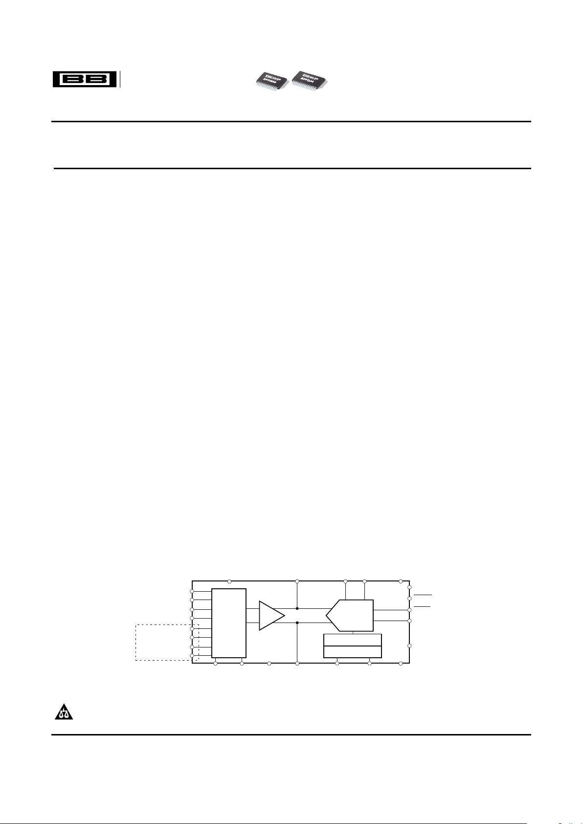
Input
Mux
DS ADC
REFP REFN
PGA
Gain=
1,2,64,or128
CAP DVDD
DGND
AGNDA1/TEMP
(1)
A0
NOTE:(1)A1forADS1234,TEMPforADS1232.
AINP1
AINN1
AINP2
AINN2
AINP3
AINN3
AINP4
AINN4
ADS1234
Only
SCLK
SPEED
DRDY/DOUT
PDWN
GAIN[1:0]
AVDD
CAP
ExternalOscillator
InternalOscillator
CLKIN/XTAL1
XTAL2
ADS1232
ADS1234
SBAS350C – JUNE 2005 – REVISED JUNE 2006
24-Bit Analog-to-Digital Converter
For Bridge Sensor
• Complete Front-End for Bridge Sensor
The ADS1232 and ADS1234 are precision 24-bit
analog-to-digital converters (ADCs). With an
• Up to 23.5 Effective Bits
onboard, low-noise programmable gain amplifier
• Onboard, Low-Noise PGA
(PGA), precision delta-sigma ADC and internal
• RMS Noise:
oscillator, the ADS1232/4 provide a complete
17nV at 10SPS (PGA = 128)
front-end solution for bridge sensor applications
44nV at 80SPS (PGA = 128)
including weigh scales, strain gauges and pressure
sensors.
• 19.2-Bit Noise-Free Resolution at Gain = 64
• Over 100dB Simultaneous 50Hz and 60Hz
The input multiplexer accepts either two (ADS1232)
or four (ADS1234) differential inputs. The ADS1232
Rejection
also includes an onboard temperature sensor to
• Flexible Clocking:
monitor ambient temperature. The onboard,
Low-Drift Onboard Oscillator ( ± 3%)
low-noise PGA has a selectable gain of 1, 2, 64, or
Optional External Crystal
128 supporting a full-scale differential input of ± 2.5V,
• Selectable Gains of 1, 2, 64, and 128
± 1.25V, ± 39mV, or ± 19.5mV. The delta-sigma ADC
has 23.5-bit effective resolution and is comprised of
• Easy Ratiometric Measurements–
a 3rd-order modulator and 4th-order digital filter. Two
External Voltage Reference up to 5V
data rates are supported: 10SPS (with both 50Hz
• Selectable 10SPS or 80SPS Data Rates
and 60Hz rejection) and 80SPS. The ADS1232/4 can
• Two-Channel Differential Input with Built-In
be clocked externally using an oscillator or a crystal.
Temperature Sensor (ADS1232)
There is also an internal oscillator available that
requires no external components. Offset calibration
• Four-Channel Differential Input (ADS1234)
is performed on-demand and the ADS1232/4 can be
• Simple Serial Digital Interface
put in a low-power standby mode or shut off
• Supply Range: 2.7V to 5.3V
completely in power-down mode. All of the features
of the ADS1232/4 are operated through simple
• –40 ° C to +105 ° C Temperature Range
pin-driven control. There are no digital registers to
program in order to simplify software development.
Data is output over an easily-isolated serial interface
• Weigh Scales
that connects directly to the MSP430 and other
• Strain Gauges
microcontrollers.
• Pressure Sensors
The ADS1232 is available in a TSSOP-24 package
• Industrial Process Control
and the ADS1234 is in a TSSOP-28. Both are fully
specified from -40 ° C to +105 ° C.
Please be aware that an important notice concerning availability, standard warranty, and use in critical applications of Texas
Instruments semiconductor products and disclaimers thereto appears at the end of this data sheet.
All trademarks are the property of their respective owners.
PRODUCTION DATA information is current as of publication date.
Copyright © 2005–2006, Texas Instruments Incorporated
Products conform to specifications per the terms of the Texas
Instruments standard warranty. Production processing does not
necessarily include testing of all parameters.
www.ti.com
ORDERING INFORMATION
ABSOLUTE MAXIMUM RATINGS
ADS1232
ADS1234
SBAS350C – JUNE 2005 – REVISED JUNE 2006
This integrated circuit can be damaged by ESD. Texas Instruments recommends that all integrated circuits be handled with
appropriate precautions. Failure to observe proper handling and installation procedures can cause damage.
ESD damage can range from subtle performance degradation to complete device failure. Precision integrated circuits may be
more susceptible to damage because very small parametric changes could cause the device not to meet its published
specifications.
For the most current package and ordering information, see the Package Option Addendum at the end of this
data sheet, or see the TI website at www.ti.com.
over operating free-air temperature range (unless otherwise noted)
(1)
ADS1232, ADS1234 UNIT
AVDD to AGND –0.3 to +6 V
DVDD to DGND –0.3 to +6 V
AGND to DGND –0.3 to +0.3 V
Input Current 100, Momentary mA
Input Current 10, Continuous mA
Analog Input Voltage to AGND –0.3 to AVDD + 0.3 V
Digital Input Voltage to DGND –0.3 to DVDD + 0.3 V
Maximum Junction Temperature +150 °C
Operating Temperature Range –40 to +105 °C
Storage Temperature Range –60 to +150 °C
(1) Stresses beyond those listed under Absolute Maximum Ratings may cause permanent damage to the device. These are stress ratings
only, and functional operation of the device at these or any other conditions beyond those indicated under Recommended Operating
Conditions is not implied. Exposure to absolute-maximum-rated conditions for extended periods may affect device reliability.
2
www.ti.com
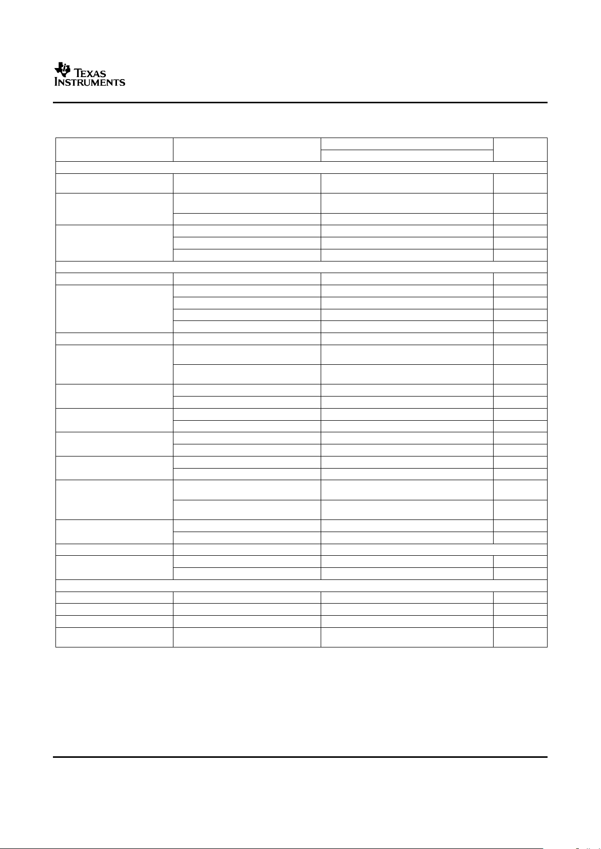
ELECTRICAL CHARACTERISTICS
ADS1232
ADS1234
SBAS350C – JUNE 2005 – REVISED JUNE 2006
All specifications at TA= –40°C to +105°C, AVDD = DVDD = VREFP = +5V, and VREFN = AGND, unless otherwise noted.
ADS1232, ADS1234
PARAMETER CONDITIONS MIN TYP MAX UNIT
Analog Inputs
Full-Scale Input Voltage
±0.5V
REF
/Gain V
(AINP – AINN)
AINxP or AINxN with respect to GND,
AGND – 0.1 AVDD + 0.1 V
Gain = 1, 2
Common-Mode Input Range
Gain = 64, 128 AGND + 1.5V AVDD – 1.5V V
Gain = 1 ± 3 nA
Differential Input Current Gain = 2 ± 6 nA
Gain = 64, 128 ± 3.5 nA
System Performance
Resolution No Missing Codes 24 Bits
Internal Oscillator, SPEED = High 78 80 82.4 SPS
Internal Oscillator, SPEED = Low 9.75 10 10.3 SPS
Data Rate
External Oscillator, SPEED = High f
CLK
/61,440 SPS
External Oscillator, SPEED = Low f
CLK
/491,520 SPS
Digital Filter Settling Time Full Settling 4 Conversions
Differential Input, End-Point Fit
± 0.0002 ± 0.001 % of FSR
(1)
Gain = 1, 2
Integral Nonlinearity (INL)
Differential Input, End-Point Fit
± 0.0004 % of FSR
Gain = 64, 128
Gain = 1 ± 0.2 ± 5 ppm of FS
Input Offset Error
(2)
Gain = 128 ± 0.02 ± 1 ppm of FS
Gain = 1 ± 0.3 µV/°C
Input Offset Drift
Gain = 128 ± 10 nV/°C
Gain = 1 ± 0.001 ± 0.02 %
Gain Error
(3)
Gain = 128 ± 0.01 ± 0.1 %
Gain = 1 ± 0.2 ppm/ ° C
Gain Drift
Gain = 128 ± 2.5 ppm/ ° C
Internal Oscillator, f
DATA
= 10SPS
100 110 dB
fIN= 50Hz or 60Hz, ± 1Hz
Normal-Mode Rejection
(4)
External Oscillator, f
DATA
= 10SPS
120 130 dB
fIN= 50Hz or 60Hz, ± 1Hz
at DC, Gain = 1, ∆ VDD = 1V 95 110 dB
Common-Mode Rejection
at DC, Gain = 128, ∆ VDD = 0.1V 95 110 dB
Input-Referred Noise See Noise Performance Tables
at DC, Gain = 1, ∆ VDD = 1V 100 120 dB
Power-Supply Rejection
at DC, Gain = 128, ∆ VDD = 0.1V 100 120 dB
Voltage Reference Input
Voltage Reference Input (V
REF
) V
REF
= VREFP – VREFN 1.5 AVDD AVDD + 0.1V V
Negative Reference Input (VREFN) AGND – 0.1 VREFP – 1.5 V
Positive Reference Input (VREFP) VREFN + 1.5 AVDD + 0.1 V
Voltage Reference
10 nA
Input Current
(1) FSR = full-scale range = V
REF
/Gain.
(2) Offset calibration can minimize these errors to the level of noise at any temperature.
(3) Gain errors are calibrated at the factory (AVDD = +5V, all gains, TA= +25 ° C).
(4) Specification is assured by the combination of design and final production test.
3
www.ti.com
ADS1232
ADS1234
SBAS350C – JUNE 2005 – REVISED JUNE 2006
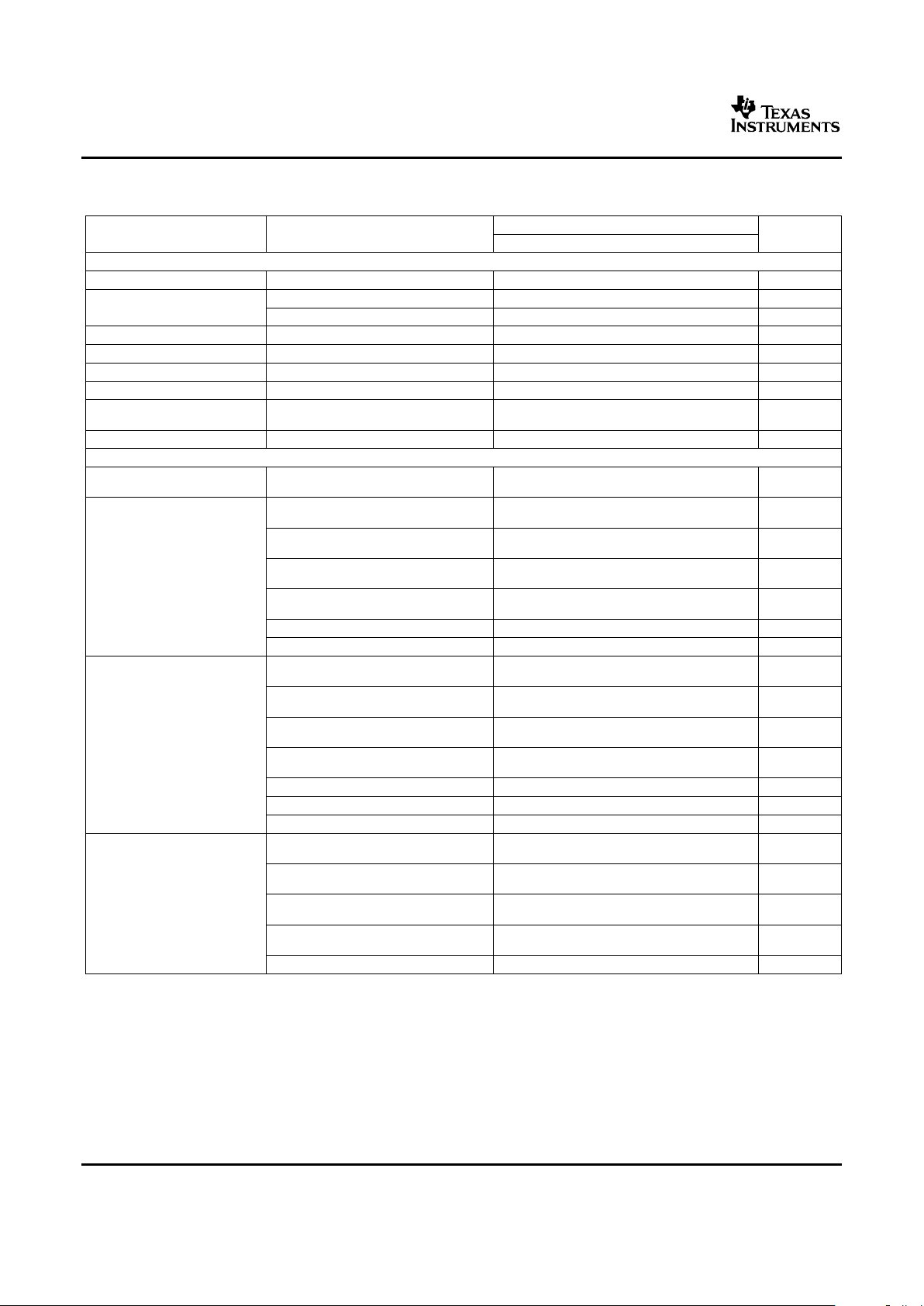
ELECTRICAL CHARACTERISTICS (continued)
All specifications at TA= –40°C to +105°C, AVDD = DVDD = VREFP = +5V, and VREFN = AGND, unless otherwise noted.
ADS1232, ADS1234
PARAMETER CONDITIONS MIN TYP MAX UNIT
Digital
Logic Levels
All digital inputs except CLKIN/XTAL1 0.7 DVDD DVDD + 0.1 V
V
IH
CLKIN/XTAL1 0.7 DVDD 5.1 V
V
IL
DGND 0.2 DVDD V
V
OH
IOH= 1mA DVDD – 0.4 V
V
OL
IOL= 1mA 0.2 DVDD V
Input Leakage 0 < VIN< DVDD ± 10 µA
External Clock Input Frequency
0.2 4.9152 8 MHz
(f
CLKIN
)
Serial Clock Input Frequency (f
SCLK
) 5 MHz
Power Supply
Power-Supply Voltage
2.7 5.3 V
(AVDD, DVDD)
Normal Mode, AVDD = 3V,
600 1300 µA
Gain = 1, 2
Normal Mode, AVDD = 3V,
1350 2500 µA
Gain = 64, 128
Normal Mode, AVDD = 5V,
650 1300 µA
Analog Supply Current
Gain = 1, 2
Normal Mode, AVDD = 5V,
1350 2500 µA
Gain = 64, 128
Standby Mode 0.1 1 µA
Power-Down 0.1 1 µA
Normal Mode, DVDD = 3V,
60 95 µA
Gain = 1, 2
Normal Mode, DVDD = 3V,
75 120 µA
Gain = 64, 128
Normal Mode, DVDD = 5V,
95 130 µA
Gain = 1, 2
Digital Supply Current
Normal mode, DVDD = 5V,
75 120 µA
Gain = 64, 128
Standby Mode, SCLK = High, DVDD = 3V 45 80 µA
Standby Mode, SCLK = High, DVDD = 5V 65 80 µ A
Power-Down 0.2 1.3 µA
Normal Mode, AVDD = DVDD = 3V,
2 4.2 mW
Gain = 1, 2
Normal Mode, AVDD = DVDD = 5V,
3.7 7.2 mW
Gain = 1, 2
Power Dissipation, Total Normal Mode, AVDD = DVDD = 3V,
4.3 7.9 mW
Gain = 64, 128
Normal Mode, AVDD = DVDD = 5V,
7.1 13.1 mW
Gain = 64, 128
Standby Mode, AVDD = DVDD = 5V 0.3 0.4 mW
4
www.ti.com
NOISE PERFORMANCE
ADS1232
ADS1234
SBAS350C – JUNE 2005 – REVISED JUNE 2006
The ADS1232/4 offer outstanding noise performance that can be optimized for a given full-scale range using the
on-chip programmable gain amplifier. Table 1 through Table 4 summarize the typical noise performance with
inputs shorted externally for different gains, data rates, and voltage reference values.
The RMS and Peak-to-Peak noise are referred to the input. The Effective Number of Bits (ENOB) is defined as:
• ENOB = ln (FSR/RMS noise)/ln(2)
The Noise-Free Bits are defined as:
• Noise-Free Bits = ln (FSR/Peak-to-Peak Noise)/ln(2)
Where FSR (Full-Scale Range) = V
REF
/Gain
Table 1. AVDD = 5V, V
REF
= 5V, Data Rate = 10SPS
GAIN RMS NOISE PEAK-TO-PEAK NOISE
(1)
ENOB (RMS) NOISE-FREE BITS
1 420nV 1.79µV 23.5 21.4
2 270nV 900nV 23.1 21.4
64 19nV 125nV 22.0 19.2
128 17nV 110nV 21.1 18.4
(1) Peak-to-peak noise data is based on direct measurement.
Table 2. AVDD = 5V, V
REF
= 5V, Data Rate = 80SPS
GAIN RMS NOISE PEAK-TO-PEAK NOISE
(1)
ENOB (RMS) NOISE-FREE BITS
1 1.36µV 8.3µV 21.8 19.2
2 850nV 5.5µV 21.5 18.8
64 48nV 307nV 20.6 18
128 44nV 247nV 19.7 17.2
(1) Peak-to-peak noise data is based on direct measurement.
Table 3. AVDD = 3V, V
REF
= 3V, Data Rate = 10SPS
GAIN RMS NOISE PEAK-TO-PEAK NOISE
(1)
ENOB (RMS) NOISE-FREE BITS
1 450nV 2.8µV 22.6 20
2 325nV 1.8µV 22.1 19.7
64 20nV 130nV 21.2 18.5
128 18nV 115nV 20.3 17.6
(1) Peak-to-peak noise data is based on direct measurement.
Table 4. AVDD = 3V, V
REF
= 3V, Data Rate = 80SPS
GAIN RMS NOISE PEAK-TO-PEAK NOISE
(1)
ENOB (RMS) NOISE-FREE BITS
1 2.2µV 12µV 20.4 17.9
2 1.2µV 6.8µV 20.2 17.8
64 54nV 340nV 19.7 17.1
128 48nV 254nV 18.9 16.5
(1) Peak-to-peak noise data is based on direct measurement of 1024 samples.
5
www.ti.com
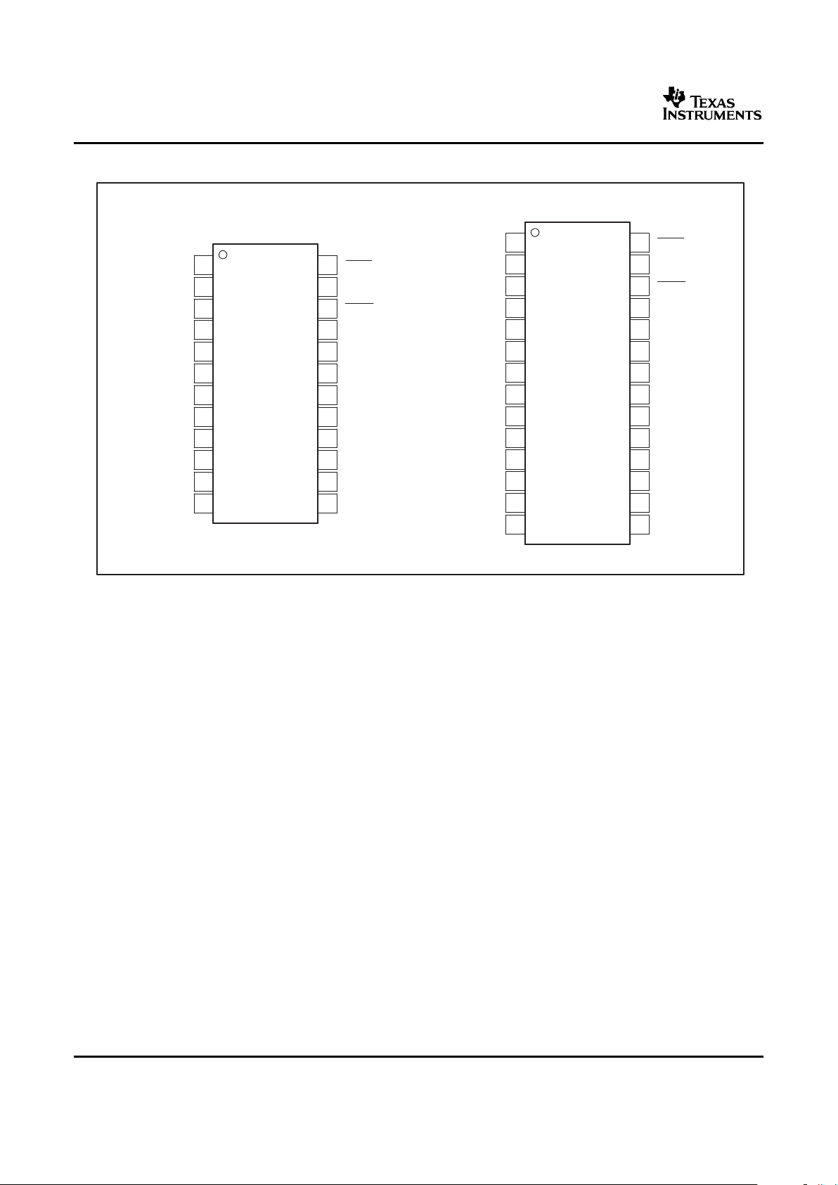
PIN CONFIGURATION
DVDD
DGND
CLKIN/XTAL1
XTAL2
DGND
DGND
A1
A0
CAP
CAP
AINP1
AINN1
AINP3
AINN3
DRDY/DOUT
SCLK
PDWN
SPEED
GAIN1
GAIN0
AVDD
AGND
REFP
REFN
AINP2
AINN2
AINP4
AINN4
1
2
3
4
5
6
7
8
9
10
11
12
13
14
28
27
26
25
24
23
22
21
20
19
18
17
16
15
ADS1234
DVDD
DGND
CLKIN/XTAL1
XTAL2
DGND
DGND
TEMP
A0
CAP
CAP
AINP1
AINN1
DRDY/DOUT
SCLK
PDWN
SPEED
GAIN1
GAIN0
AVDD
AGND
REFP
REFN
AINP2
AINN2
1
2
3
4
5
6
7
8
9
10
11
12
24
23
22
21
20
19
18
17
16
15
14
13
ADS1232
ADS1232
ADS1234
SBAS350C – JUNE 2005 – REVISED JUNE 2006
6
www.ti.com
ADS1232
ADS1234
SBAS350C – JUNE 2005 – REVISED JUNE 2006
PIN CONFIGURATION (continued)
PIN DESCRIPTIONS
TERMINAL
ANALOG/DIGITAL
NAME ADS1232 ADS1234 INPUT/OUTPUT DESCRIPTION
DVDD 1 1 Digital Digital Power Supply: 2.7V to 5.3V
DGND 2 2 Digital Digital Ground
CLKIN/ External Clock Input: typically 4.9152MHz. Tie low to activate internal oscillator. Can also use
3 3 Digital/Digital Input
XTAL1 external crystal across CLKIN/XTAL1 and XTAL2 pins. See text for more details.
XTAL2 4 4 Digital External crystal connection
DGND 5 5 Digital Digital Ground
DGND 6 6 Digital Digital Ground
TEMP 7 – Digital Input Onboard Temperature Diode Enable
Input Mux Select Input pin (MSB)
Input Mux Select Input pin (LSB):
A1 A0 Channel
A1 – 7
Digital Input 0 0 AIN1
A0 8 8
0 1 AIN2
1 0 AIN3
1 1 AIN4
CAP 9 9 Analog Gain Amp Bypass Capacitor Connection
CAP 10 10 Analog Gain Amp Bypass Capacitor Connection
AINP1 11 11 Analog Input Positive Analog Input Channel 1
AINN1 12 12 Analog Input Negative Analog Input Channel 1
AINP3 – 13 Analog Input Positive Analog Input Channel 3
AINN3 – 14 Analog Input Negative Analog Input Channel 3
AINN4 – 15 Analog Input Negative Analog Input Channel 4
AINP4 – 16 Analog Input Positive Analog Input Channel 4
AINN2 13 17 Analog Input Negative Analog Input Channel 2
AINP2 14 18 Analog Input Positive Analog Input Channel 2
REFN 15 19 Analog Input Negative Reference Input
REFP 16 20 Analog Input Positive Reference Input
AGND 17 21 Analog Analog Ground
AVDD 18 22 Analog Analog Power Supply, 2.7V to 5.3V
Gain Select
GAIN1 GAIN0 GAIN
0 0 1
GAIN0 19 23
Digital Input
GAIN1 20 24
0 1 2
1 0 64
1 1 128
Data Rate Select:
SPEED DATA RATE
SPEED 21 25 Digital Input
0 10SPS
1 80SPS
PDWN 22 26 Digital Input Power-Down: Holding this pin low powers down the entire converter and resets the ADC.
Serial Clock: Clock out data on the rising edge. Also used to initiate Offset Calibration and Sleep
SCLK 23 27 Digital Input
modes. See text for more details.
Dual-Purpose Output:
DRDY/
24 28 Digital Output Data Ready: Indicates valid data by going low.
DOUT
Data Output: Outputs data, MSB first, on the first rising edge of SCLK.
7
www.ti.com
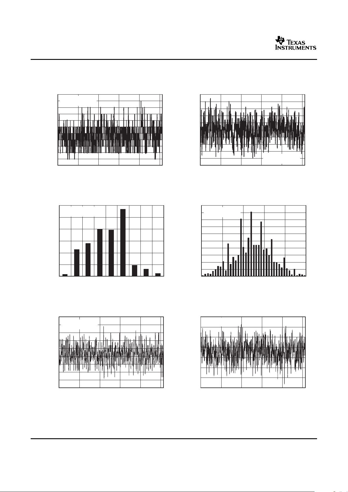
TYPICAL CHARACTERISTICS
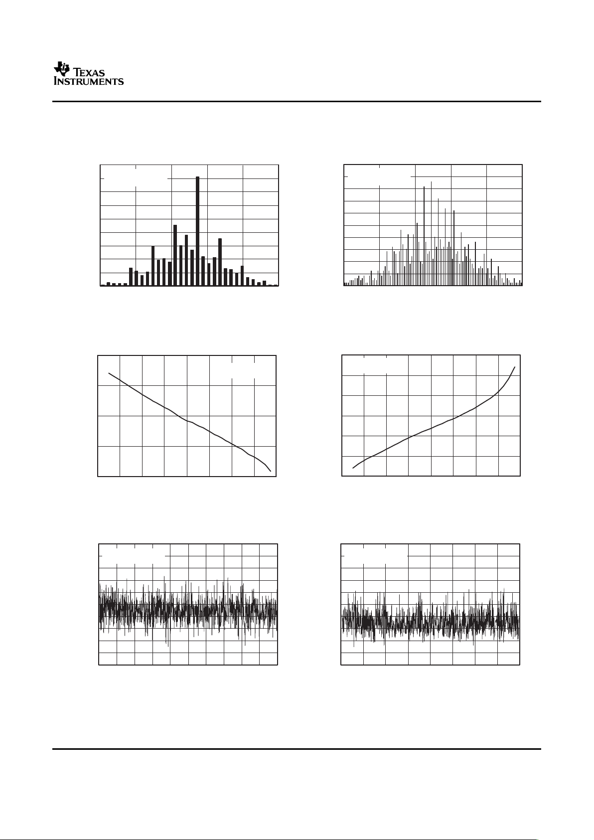
Time (Reading Number)
Output Code (LSB)
6
5
4
3
2
1
−
1
−
2
−
3
−
4
−
5
−
6
200 400 600 800 1000
0
PGA = 1
Data Rate = 10SPS
Time (Reading Number)
Output Code (LSB)
25
20
15
10
5
0
−
5
−
10
−
15
−
20
−
25
200 400 600 800 1000
0
PGA = 128
Data Rate = 10SPS
Output Code (LSB)
Occurrence
300
250
200
150
100
50
0
−
4
−
2
0
2
4
PGA = 1
Data Rate = 10SPS
Output Code (LSB)
Occurrence
100
90
80
70
60
50
40
30
20
10
0
−
16
1680
−
8
PGA = 128
Data Rate = 10SPS
Time (Reading Number)
Output Code(LSB)
22.5
17.5
12.5
7.5
2.5
−
2.5
−
7.5
−
12.5
−
17.5
−
22.5
200 400 600 800 1000
0
PGA = 1
Data Rate = 80SPS
Time (Reading Number)
Output Code (LSB)
70
50
30
10
−
10
−
30
−
50
−
70
200 400 600 800 1000
0
PGA = 128
Data Rate = 80SPS
ADS1232
ADS1234
SBAS350C – JUNE 2005 – REVISED JUNE 2006
At TA= +25 ° C, AVDD = DVDD = VREFP = 5V, and VREFN = AGND, unless otherwise noted.
NOISE PLOT NOISE PLOT
Figure 1. Figure 2.
NOISE HISTOGRAM NOISE HISTOGRAM
Figure 3. Figure 4.
NOISE PLOT NOISE PLOT
Figure 5. Figure 6.
8
www.ti.com
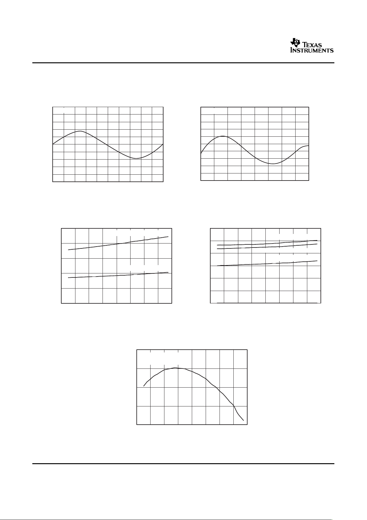
Output Code (LSB)
Occurance
180
160
140
120
100
80
60
40
20
0
−
12
−
6
1260
PGA = 1
Data Rate = 80SPS
Output Code (LSB)
Occurance
50
45
40
35
30
25
20
15
10
5
0
−
40
−
20 0 20
40
PGA = 128
Data Rate = 80SPS
Temperature (_C)
Offset (nV)
1000
500
0
−
500
−
1000
110
−50−30−
10 10 30 50 70 90
PGA = 128
Data Rate = 10SPS
Temperature (_C)
Gain Error (%)
0.04
0.03
0.02
0.01
0
−
0.01
−
0.02
110
−50−30−
10 10 30 50 70 90
PGA = 128
Data Rate = 10SPS
VIN(V)
RMS Noise (nV)
1000
900
800
700
600
500
400
300
200
100
0
2.5
−
2.5−2.0−1.5
−
0.5
−
1.0 1.00 0.5 1.5 2.0
PGA = 1
Data Rate = 10SPS
VIN(mV)
RMS Noise (nV)
50
45
40
35
30
25
20
15
10
5
0
19
−19−
14.25−9.5−4.75 4.750 9.5 14.25
PGA = 128
Data Rate = 10SPS
ADS1232
ADS1234
SBAS350C – JUNE 2005 – REVISED JUNE 2006
TYPICAL CHARACTERISTICS (continued)
At TA= +25 ° C, AVDD = DVDD = VREFP = 5V, and VREFN = AGND, unless otherwise noted.
NOISE HISTOGRAM NOISE HISTOGRAM
Figure 7. Figure 8.
OFFSET vs TEMPERATURE GAIN ERROR vs TEMPERATURE
Figure 9. Figure 10.
NOISE vs INPUT SIGNAL NOISE vs INPUT SIGNAL
Figure 11. Figure 12.
9
www.ti.com
VIN(mV)
INL (ppmof FSR)
INL (nV)
10
8
6
4
2
0
−
2
−
4
−
6
−
8
−
10
390.625
312.5
234.375
156.25
78.125
0
−
78.125
−
156.25
−
234.375
−
312.5
−
390.625
19
−19−
14.25−9.5−4.75 4.750 9.5 14.25
PGA = 128
VIN(V)
INL (ppm of FSR)
INL (
µ
V)
5
4
3
2
1
0
−
1
−
2
−
3
−
4
−
5
25
20
15
10
5
0
−
5
−
10
−
15
−
20
−
25
2.5
−
2.5−2.0−1.5
−
0.5
−
1.0 1.00 0.5 1.5 2.0
PGA = 1
Temperature (_C)
Analog Current (
µ
A)
2000
1600
1200
800
400
0
110
−50−30−
10 10 30 50 70 90
Normal Mode, PGA = 64, 128
Normal Mode, PGA = 1, 2
Temperature (_C)
Digital Current (
µ
A)
120
100
80
60
40
20
0
110
−50−30−
10 10 30 50 70 90
Normal Mode, PGA = 64, 128
Normal Mode, PGA = 1, 2
Sleep Mode, All PGAs
Temperature (_C)
Data Rate (SPS)
10.06
10.01
9.96
9.91
9.86
110
−50−30−
10 10 30 50 70 90
SPEED = LOW
CLKIN/XTAL1 = LOW (Internal Oscillator)
ADS1232
ADS1234
SBAS350C – JUNE 2005 – REVISED JUNE 2006
TYPICAL CHARACTERISTICS (continued)
At TA= +25 ° C, AVDD = DVDD = VREFP = 5V, and VREFN = AGND, unless otherwise noted.
INTEGRAL NONLINEARITY INTEGRAL NONLINEARITY
vs INPUT SIGNAL vs INPUT SIGNAL
Figure 13. Figure 14.
ANALOG CURRENT DIGITAL CURRENT
vs TEMPERATURE vs TEMPERATURE
Figure 15. Figure 16.
DATA RATE
vs TEMPERATURE
Figure 17.
10
www.ti.com
TEMPERATURE SENSOR (ADS1232 only)
OVERVIEW
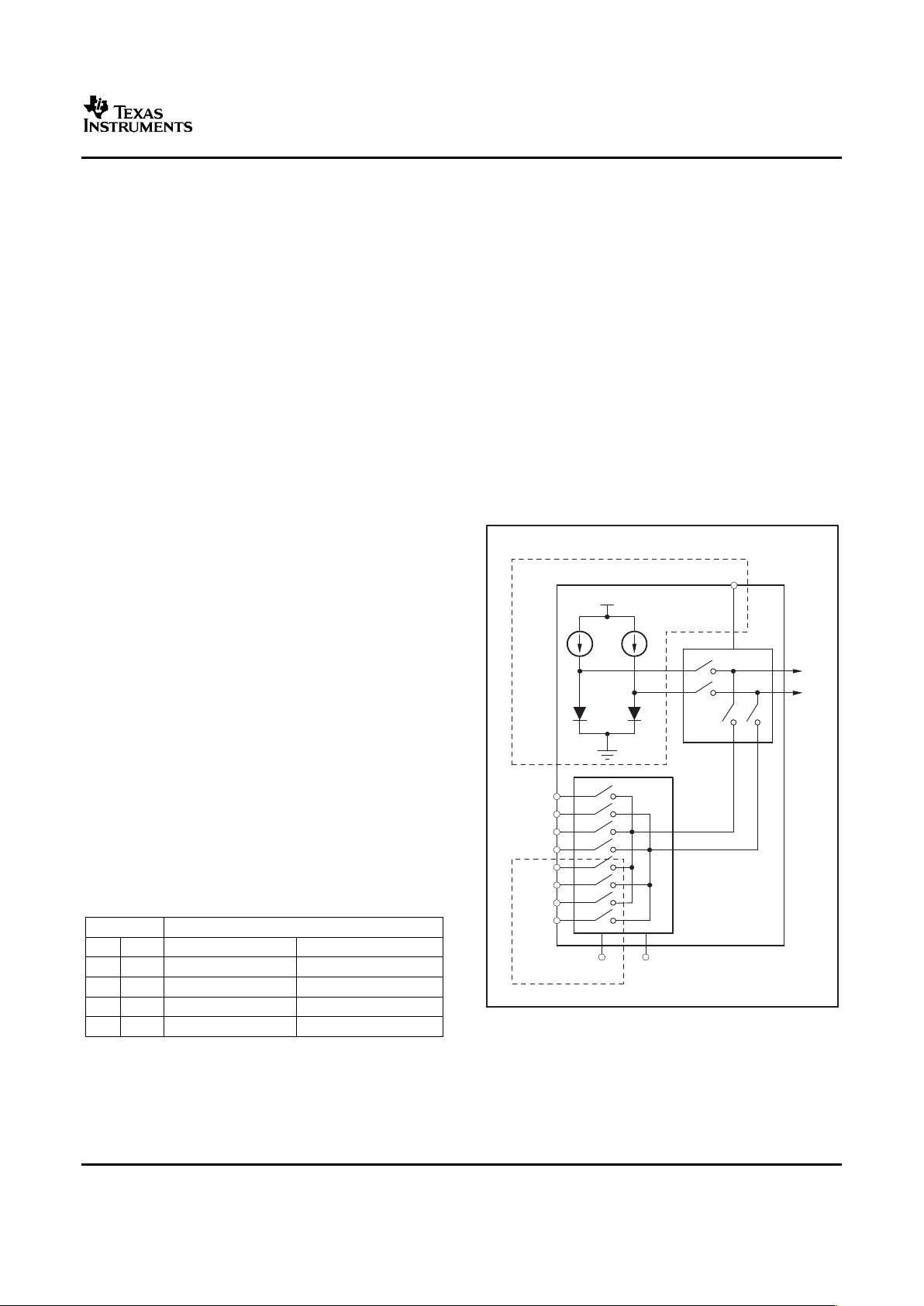
ANALOG INPUTS (AINPx, AINNx)
A0A1
AINP
AINP1
AINN1
AINP2
AINN2
AINP3
AINN3
AINP4
AINN4
10I 1I
1X 8X
AINN
ADS1232 Only
AVDD
ADS1234 Only
ADS1232
ADS1234
SBAS350C – JUNE 2005 – REVISED JUNE 2006
On-chip diodes provide temperature-sensing
capability. By setting the TEMP pin high, the
The ADS1232 and ADS1234 are highly integrated,
selected analog inputs are disconnected and the
24-bit ADCs that include an input multiplexer,
inputs to the ADC are connected to the anodes of
low-noise PGA, third-order delta-sigma ( ∆ Σ )
two diodes scaled to 1x and 80x in current and size,
modulator, and fourth-order digital filter. With
as shown in Figure 18 . By measuring the difference
input-referred RMS noise down to 17nV, the
in voltage of these diodes, temperature changes can
ADS1232/4 are ideally suited for measuring the very
be inferred from a baseline temperature. Typically,
low signals produced by bridge sensors in
the difference in diode voltage is 111.7mV at 25 ° C
applications such as weigh scales, strain gauges,
with a temperature coefficient of 379 µ V/ ° C. With
and pressure sensors.
PGA = 1 and 2, the difference voltage output from
Clocking can be supplied by an external oscillator,
the PGA will be 111.7mV and 323.4mV, respectively.
an external crystal, or by a precision internal
With PGA = 64 and 128, it is impossible to use the
oscillator. Data can be output at 10SPS for excellent
temperature sensor function. A similar structure is
50Hz and 60Hz rejection, or at 80SPS when higher
used in the MSC1210 for temperature measurement.
speeds are needed. The ADS1232/4 are easy to
For more information, see TI application report
configure, and all digital control is accomplished
SBAA100 , Using the MSC121x as a High-Precision
through dedicated pins; there are no registers to
Intelligent Temperature Sensor, available for
program. A simple two-wire serial interface retrieves
download at www.ti.com .
the data.
The input signal to be measured is applied to the
input pins AINPx and AINNx. The positive internal
input is generalized as AINP, and the negative
internal input generalized as AINN. The signal is
selected through the input mux, which is controlled
by pins A0 and A1 (ADS1234 only), as shown in
Table 5 . For the ADS1232, the A1 pin is replaced by
the TEMP pin to activate the onboard diodes (see
the Temperature Sensor section for more details).
The ADS1232/4 accept differential input signals, but
can also measure unipolar signals. When measuring
unipolar (or single-ended signals) with respect to
ground, connect the negative input (AINNx) to
ground and connect the input signal to the positive
input (AINPx). Note that when the ADS1232/4 are
configured this way, only half of the converter
full-scale range is used, since only positive digital
output codes are produced.
Table 5. Input Channel Selection with A0 and A1
(ADS1234 only)
MUX PINS SELECTED ANALOG INPUTS
A1 A0 POSITIVE INPUT NEGATIVE INPUT
0 0 AINP1 AINN1
0 1 AINP2 AINN2
1 0 AINP3 AINN3
1 1 AINP4 AINN3
Figure 18. Measurement of the Temperature
Sensor in the Input Multiplexer
11

www.ti.com
LOW-NOISE PGA
VOLTAGE REFERENCE INPUTS
Z
EFF
+
1
2f
MOD
C
BUF
Z
EFF
+
1
(2)(76.8kHz)(32.5fF)
+ 200MW
R
INT
R
INT
R
F1
R
1
R
F2
ADC
A3
Gainof1or2
CAP
AINP
AINN
CAP
A2
A1
450W
18pF
450W
18pF
AVDD
(1) f
MOD
= 76.8kHz
Z
EFF
= 200M
Ω
(1)
VREFP VREFN
AVDD
ESD
Protection
C
BUF
Bypass Capacitor
ADS1232
ADS1234
SBAS350C – JUNE 2005 – REVISED JUNE 2006
attenuates the chopping residue from the PGA (for
gains of 64 and 128 only) to improve temperature
The ADS1232/4 features a low-drift, low-noise PGA
drift performance. It is not required to use high
that provides a complete front-end solution for bridge
quality capacitors (such as ceramic or tantalum
sensors. A simplified diagram of the PGA is shown in
capacitors) for a general application. However, high
Figure 19 . It consists of two chopper-stabilized
quality capacitors such as poly are recommended for
amplifiers (A1 and A2) and three accurately-matched
high linearity applications.
resistors (R
1
, R
F1
, and R
F2
), which construct a
differential front-end stage with a gain of 64, followed
by gain stage A3. The PGA inputs are equipped with
(REFP, REFN)
an EMI filter, as shown in Figure 19 . The cut-off
frequency of the EMI filter is 19.6MHz. If the PGA is
The voltage reference used by the modulator is
set to 1 or 2, the gain-of-64 stage is bypassed and
generated from the voltage difference between
shut down to save power. With the combination of
REFP and REFN: V
REF
= REFP – REFN. The
both gain stages, the PGA can be set to 64 or 128.
reference inputs use a structure similar to that of the
The PGA of the ADS1232/4 can be set to 1, 2, 64, or
analog inputs. In order to increase the reference
128 with pins GAIN1 (MSB) and GAIN0 (LSB). By
input impedance, a switching buffer circuitry is used
using AVDD as the reference input, the bipolar input
to reduce the input equivalent capacitance. A
ranges from ± 2.5V to ± 19.5mV, while the unipolar
simplified diagram of the circuitry on the reference
ranges from 2.5V to 19.5mV. When the PGA is set to
inputs is shown in Figure 20 . The switches and
1 or 2, the absolute inputs can go rail-to-rail without
capacitors can be modeled with an effective
significant performance degradation. However, the
impedance of:
inputs of the ADS1232/4 are protected with internal
diodes connected to the power-supply rails. These
diodes will clamp the applied signal to prevent it from
damaging the input circuitry. On the other hand,
Where:
when the PGA is set to 64 or 128, the operating
f
MOD
= modulator sampling frequency (76.8kHz)
input range is limited to (AGND + 1.5V) to (AVDD –
C
BUF
= input capacitance of the buffer
1.5V), in order to prevent saturating the differential
front-end circuitry and degrading performance.
For the ADS1232/4:
Figure 19. Simplified Diagram of the PGA
Figure 20. Simplified Reference Input Circuitry
ESD diodes protect the reference inputs. To prevent
By applying a 0.1µF external capacitor (C
EXT
) across
these diodes from turning on, make sure the
two capacitor pins and the combination of the
voltages on the reference pins do not go below GND
internal 2k Ω resistor R
INT
on-chip, a low-pass filter
by more than 100mV, and likewise, do not exceed
(with a corner frequency of 720Hz) is created to
AVDD by 100mV:
bandlimit the signal path prior to the modulator input.
This low-pass filter serves two purposes. First, the
GND – 100mV < (REFP or REFN) < AVDD + 100mV
input signal is bandlimited to prevent aliasing as well
as to filter out the high-frequency noise. Second, it
12

www.ti.com
CLOCK SOURCES
CLK_DETECT
Internal
Oscillator
MUX
To ADC
S
S0 S1
EN
Crystal
Oscillator
CLKIN/XTAL1
XTAL2
ADS1232
ADS1234
SBAS350C – JUNE 2005 – REVISED JUNE 2006
When the clock source is a crystal, simply connect
the 4.9152MHz crystal across the CLKIN/XTAL1 and
The ADS1232/4 can use an external clock source,
XTAL2 pins. Table 6 shows the recommended part
external crystal, or internal oscillator to
numbers. Due to the low-power design of the parallel
accommodate a wide variety of applications.
resonant driver circuitry onboard, both the
Figure 21 shows the equivalent circuitry of the clock
CLKIN/XTAL1 and XTAL2 pins are only for use with
source. The CLK_DETECT block determines
external crystals; they should not be used as clock
whether the crystal oscillator/external clock signal is
output drivers for external circuitry. No external
applied to the CLKIN/XTAL1 pin so that the internal
capacitors are used with the crystal; it is
oscillator is bypassed or activated. When the
recommended to place the crystal close to the part in
CLKIN/XTAL1 pin frequency is above ~200kHz, the
order to reduce board stray capacitance for both the
CLK_DETECT output goes low and shuts down the
CLKIN/XTAL1 and XTAL2 pins and to insure proper
internal oscillator. When the XIN pin frequency is
operation.
below ~200kHz, the CLK_DETECT output goes high
and activates the internal oscillator. It is highly
Table 6. Recommended Crystals
recommended to hard-wire the CLKIN/XTAL1 pin to
MANUFACTURER FREQUENCY PART NUMBER
ground when the internal oscillator is chosen.
ECS 4.9152MHz ECS-49-20-1
ECS 4.9152MHz ECS-49-20-4
An external oscillator may be used by driving the
CLKIN/XTAL1 pin directly. The Electrical
Characteristics table shows the allowable frequency
range. The clock input may be driven with 5V logic,
regardless of the DVDD or AVDD voltage.
Figure 21. Equivalent Circuitry of the Clock
Source
13

www.ti.com
FREQUENCY RESPONSE
Frequency (kHz)
Gain (dB)
0
−
20
−
40
−
60
−
80
−
100
−
120
−
140
−
160
−
180
−
200
38.4 76.8
0
f
CLK
= 4.9152MHz
Frequency (Hz)
Gain (dB)
0
−
50
−
100
−
150
0 10 20 30 40 50 60 70 80 90 100
(a)
Frequency (Hz)
(b)
Gain (dB)
−
50
−
100
−
150
494846 47 50 51 52 53 54 55 56 57 58 59 60 61 62 63 64
Data Rate = 10SPS
Data Rate =10SPS
ADS1232
ADS1234
SBAS350C – JUNE 2005 – REVISED JUNE 2006
Figure 23 (b) shows the zoom in plot for both 50Hz
and 60Hz notches with the SPEED pin tied low
The ADS1232/4 use a sinc
4
digital filter with the
(10SPS data rate). With only a ± 3% variation of the
frequency response (f
CLK
= 4.9152MHz) shown in
internal oscillator, over 100dB of normal-mode
Figure 22 . The frequency response repeats at
rejection is achieved.
multiples of the modulator sampling frequency of
76.8kHz. The overall response is that of a low-pass
filter with a –3dB cutoff frequency of 3.32Hz with the
SPEED pin tied low (10SPS data rate) and 11.64Hz
with the SPEED pin tied high (80SPS data rate).
Figure 22. Frequency Response
To help see the response at lower frequencies,
Figure 23 (a) illustrates the response out to 100Hz,
when the data rate = 10SPS. Notice that signals at
multiples of 10Hz are rejected, and therefore
simultaneous rejection of 50Hz and 60Hz is
achieved.
Figure 23. Frequency Response Out To 100Hz
The benefit of using a sinc
4
filter is that every
frequency notch has four zeros on the same location.
This response, combined with the low drift internal
The ADS1232/4 data rate and frequency response
oscillator, provides an excellent normal-mode
scale directly with clock frequency. For example, if
rejection of line-cycle interference.
f
CLK
increases from 4.9152MHz to 6.144MHz when
the SPEED pin is tied high, the data rate increases
from 80SPS to 100SPS, while notches also increase
from 80Hz to 100Hz. Note that this is only possible
when the external clock source is applied.
14

www.ti.com
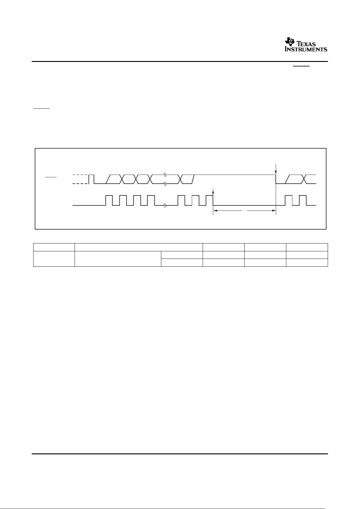
SETTLING TIME
A1, A0, or TEMP change
t
1
DRDY/DOUT
t
S
Abrupt Change in External V
IN
V
IN
DRDY/DOUT
Start of
Conversion
1st Conversion;
includes
unsettled VIN.
2nd Conversion;
VINsettled, but
digital filter
unsettled.
3rd Conversion;
VINsettled, but
digital filter
unsettled.
4th Conversion;
VINsettled, but
digital filter
unsettled.
5th Conversion;
VINand digital
filter both
settled.
Conversion
Time
ADS1232
ADS1234
SBAS350C – JUNE 2005 – REVISED JUNE 2006
In certain instances, large changes in input will
require settling time. For example, an external
After changing the input multiplexer, or selecting the
multiplexer in front of the ADS1232/4 can put large
onboard temperature sensor (ADS1232 only), the
changes in input voltage by simply switching input
first data is fully settled. In both the ADS1232/4, the
channels. Abrupt changes in the input will require
digital filter is allowed to settle after toggling any of
four data cycles to settle. When continuously
the A1, A0, or TEMP pins. Toggling any of these
converting, five readings may be necessary in order
digital pins will hold the DRDY/DOUT line high until
to settle the data. If the change in input occurs in the
the digital filter is fully settled. For example, if A0
middle of the first conversion, four more full
changes from low to high, selecting a different input
conversions of the fully-settled input will be required
channel, DRDY/DOUT immediately goes high, and
to get fully-settled data. Discard the first four
DRDY/DOUT goes low when fully-settled data is
readings because they will contain only
ready for retrieval. There is no need to discard any
partially-settled data. Figure 25 illustrates the settling
data. Figure 24 shows the timing of the DRDY/DOUT
time for the ADS1232/4 in Continuous Conversion
line as the input multiplexer changes.
Mode.
Figure 24. Example of Settling Time After Changing the Input Multiplexer
SYMBOL DESCRIPTION
(1)
MIN MAX UNITS
t
S
Setup time for changing any of the A1, A0, or TEMP pins 40 50 µ s
SPEED = 1 51 51 ms
Settling time ( DRDY/DOUT
t
1
held high)
SPEED = 0 401 401 ms
(1) Values given for f
CLK
= 4.9152MHz. For different f
CLK
frequencies, scale proportional to CLK period. Expect a ± 3% variation when an
internal oscillator is used.
Figure 25. Settling Time in Continuous Conversion Mode
15

www.ti.com
DATA RATE
DATA FORMAT
DATA READY/DATA OUTPUT ( DRDY/DOUT) SERIAL CLOCK INPUT (SCLK)
ADS1232
ADS1234
SBAS350C – JUNE 2005 – REVISED JUNE 2006
Table 7. Data Rate Settings
DATA RATE
The ADS1232/4 data rate is set by the SPEED pin,
SPEED
Internal Oscillator External
as shown in Table 7 . When SPEED is low, the data
PIN
or 4.9152MHz Crystal Oscillator
rate is nominally 10SPS. This data rate provides the
lowest noise, and also has excellent rejection of both 0 10SPS f
CLKIN
/ 491,520
50Hz and 60Hz line-cycle interference. For
1 80SPS f
CLKIN
/ 61,440
applications requiring fast data rates, setting SPEED
high selects a data rate of nominally 80SPS.
Table 8. Ideal Output Code vs Input Signal
(1)
The ADS1232/4 output 24 bits of data in binary two’s
INPUT SIGNAL V
IN
complement format. The least significant bit (LSB)
(AINP – AINN) IDEAL OUTPUT CODE
has a weight of 0.5V
REF
/(2
23
– 1). The positive
≥ +0.5V
REF
/Gain 7FFFFFh
full-scale input produces an output code of 7FFFFFh
and the negative full-scale input produces an output
(+0.5V
REF
/Gain)/(2
23
– 1) 000001h
code of 800000h. The output clips at these codes for
0 000000h
signals exceeding full-scale. Table 8 summarizes the
(–0.5V
REF
/Gain)/(2
23
– 1) FFFFFFh
ideal output codes for different input signals.
≤ – 0.5V
REF
/Gain 800000h
(1) Excludes effects of noise, INL, offset, and gain errors.
This digital output pin serves two purposes. First, it This digital input shifts serial data out with each
indicates when new data is ready by going low. rising edge. As with CLK, this input may be driven
Afterwards, on the first rising edge of SCLK, the with 5V logic regardless of the DVDD or AVDD
DRDY/DOUT pin changes function and begins voltage. This input has built-in hysteresis, but care
outputting the conversion data, most significant bit should still be taken to ensure a clean signal.
(MSB) first. Data is shifted out on each subsequent Glitches or slow-rising signals can cause unwanted
SCLK rising edge. After all 24 bits have been additional shifting. For this reason, it is best to make
retrieved, the pin can be forced high with an sure the rise-and-fall times of SCLK are less than
additional SCLK. It will then stay high until new data 50ns.
is ready. This configuration is useful when polling on
the status of DRDY/DOUT to determine when to
begin data retrieval.
16

www.ti.com
DATA RETRIEVAL
DRDY/DOUT 23 22 21
1 24
0
LSBMSB
Data
Data Ready
SCLK
t
2
t
7
t
3
t
3
t
6
New Data Ready
t
4
t
5
23
1 24 25
22 21 0
Data
25th SCLK to Force DRDY/DOUT High
Data Ready New Data Ready
DRDY/DOUT
SCLK
ADS1232
ADS1234
SBAS350C – JUNE 2005 – REVISED JUNE 2006
last bit shifted out until it is taken high (see t6),
indicating that new data is being updated. To avoid
The ADS1232/4 continuously convert the analog
having DRDY/DOUT remain in the state of the last
input signal. To retrieve data, wait until DRDY/DOUT
bit, the user can shift SCLK to force DRDY/DOUT
goes low, as shown in Figure 26 . After this occurs,
high, as shown in Figure 27 . This technique is useful
begin shifting out the data by applying SCLKs. Data
when a host controlling the device is polling
is shifted out MSB first. It is not required to shift out
DRDY/DOUT to determine when data is ready.
all 24 bits of data, but the data must be retrieved
before new data is updated (within t7) or else it will
be overwritten. Avoid data retrieval during the update
period (t6). DRDY/DOUT remains at the state of the
Figure 26. Data Retrieval Timing
SYMBOL DESCRIPTION MIN TYP MAX UNITS
t
2
DRDY/DOUT low to first SCLK rising edge 0 ns
t
3
SCLK positive or negative pulse width 100 ns
t
4
SCLK rising edge to new data bit valid: propagation 50 ns
delay
t
5
SCLK rising edge to old data bit valid: hold time 0 ns
t
6
(1)
Data updating: no readback allowed 39 µ s
SPEED = 1 12.5 ms
t
7
(1)
Conversion time (1/data rate)
SPEED = 0 100 ms
(1) Values given for f
CLK
= 4.9152MHz. For different f
CLK
frequencies, scale proportional to CLK period.
Figure 27. Data Retrieval with DRDY/DOUT Forced High Afterwards
17
www.ti.com
OFFSET CALIBRATION
23DRDY/DOUT
SCLK
1 24
t
8
25 26
2322 21 0
Data Ready AfterCalibration
Calibration Begins
ADS1232
ADS1234
SBAS350C – JUNE 2005 – REVISED JUNE 2006
When the calibration is completed, DRDY/DOUT
goes low, indicating that new data is ready. The
Offset calibration can be initiated at any time to
analog input pins are disconnected within the ADC
remove the ADS1232/4 inherited offset error. To
and the appropriate signal is applied internally to
initiate offset calibration, apply at least two additional
perform the calibration. The first conversion after a
SCLKs after retrieving 24 bits of data. Figure 28
calibration is fully settled and valid for use. The offset
shows the timing pattern. The 25th SCLK will send
calibration takes exactly the same time as specified
DRDY/DOUT high. The falling edge of the 26th
in (t8) right after the falling edge of the 26th SCLK.
SCLK will begin the calibration cycle. Additional
SCLK pulses may be sent after the 26th SCLK;
however, activity on SCLK should be minimized
during offset calibration for best results.
Figure 28. Offset-Calibration Timing
SYMBOL DESCRIPTION MIN MAX UNITS
SPEED = 1 101.28 101.29 ms
t
8
(1)
First data ready after calibration
SPEED = 0 801.02 801.03 ms
(1) Values given for f
CLK
= 4.9152MHz. For different f
CLK
frequencies, scale proportional to CLK period. Expect a ± 3% variation when an
internal oscillator is used.
18

www.ti.com
STANDBY MODE
DRDY/DOUT 23 22 21
1 24
0 23
SCLK
Standby Mode
Start Conversion
Data Ready
t
9
t
10
t
11
ADS1232
ADS1234
SBAS350C – JUNE 2005 – REVISED JUNE 2006
When t10has passed with SCLK held high, Standby
mode will activate. DRDY/DOUT stays high when
Standby mode dramatically reduces power
Standby mode begins. SCLK must remain high to
consumption by shutting down most of the circuitry.
stay in Standby mode. To exit Standby mode
In Standby mode, the entire analog circuitry is
(wakeup), set SCLK low. The first data after exiting
powered down and only the clock source circuitry is
Standby mode is valid.
awake to reduce the wake-up time from the Standby
mode. To enter Standby mode, simply hold SCLK
high after DRDY/DOUT goes low; see Figure 29 .
Standby mode can be initiated at any time during
readback; it is not necessary to retrieve all 24 bits of
data beforehand.
Figure 29. Standby Mode Timing (can be used for single conversions)
SYMBOL DESCRIPTION MIN MAX UNITS
SPEED = 1 0 12.44 ms
SCLK high after DRDY/DOUT goes
t
9
(1)
low to activate Standby mode
SPEED = 0 0 99.94 ms
SPEED = 1 12.46 ms
t
10
(1)
Standby mode activation time
SPEED = 0 99.96 ms
SPEED = 1 52.51 52.51 ms
t
11
(1)
Data ready after exiting Standby mode
SPEED = 0 401.8 401.8 ms
(1) Values given for f
CLK
= 4.9152MHz. For different f
CLK
frequencies, scale proportional to CLK period. Expect a ± 3% variation when an
internal oscillator is used.
19

www.ti.com
STANDBY MODE WITH
Standby Mode
Begin Calibration
Data Ready After Calibration
t
10
t
12
DRDY/DOUT 23
1 24 25
22 21 0 23
SCLK
ADS1232
ADS1234
SBAS350C – JUNE 2005 – REVISED JUNE 2006
To force an offset-calibration with Standby mode,
OFFSET-CALIBRATION shift 25 SCLKs and take the SCLK pin high to enter
Standby mode. Offset-calibration then begins after
Offset-calibration can be set to run immediately after
wake-up; see Figure 30 for the appropriate timing.
exiting Standby mode. This is useful when the
Note the extra time needed after wake-up for
ADS1232/4 is put in Standby mode for long periods
calibration before data is ready. The first data after
of time, and offset-calibration is desired afterwards to
Standby mode with offset-calibration is fully settled
compensate for temperature or supply voltage
and can be used right away.
changes.
Figure 30. Standby Mode with Offset-Calibration Timing (can be used for single conversions)
SYMBOL DESCRIPTION MIN MAX UNITS
t
12
(1)
SPEED = 1 103 103 ms
Data ready after exiting Standby mode
and calibration
SPEED = 0 803 803 ms
(1) Values given for f
CLK
= 4.9152MHz. For different f
CLK
frequencies, scale proportional to CLK period. Expect a ± 3% variation when an
internal oscillator is used.
20

www.ti.com
POWER-DOWN MODE
DataReady
Start
Conversion
DRDY/DOUT
SCLK
CLKSoure
WakeupPower-DownMode
PDWN
t
13
t
11
t
14
ADS1232
ADS1234
SBAS350C – JUNE 2005 – REVISED JUNE 2006
from locking up to an unknown state. Power-Down
mode can be initiated at any time during readback; it
Power-Down mode shuts down the entire ADC
is not necessary to retrieve all 24 bits of data
circuitry and reduces the total power consumption
beforehand. Figure 31 shows the wake-up timing
close to zero. To enter Power-Down mode, simply
from Power-Down mode.
hold the PDWN pin low. Power-Down mode also
resets the entire circuitry to free the ADC circuitry
Figure 31. Wake-Up Timing from Power-Down Mode
SYMBOL DESCRIPTION TYP UNITS
Internal clock 7.95 µ s
t
13
Wake-up time after Power-Down mode External clock 0.16 µ s
Crystal oscillator
(1)
5.6 ms
t
14
(2)
PDWN pulse width 26 (min) µ s
(1) No capacitors on CLKIN/XTAL1 or XTAL2 outputs.
(2) Value given for f
CLK
= 4.9152MHz. For different f
CLK
frequencies, the scale is proportional to the CLK period except for a ± 3% variation
when an internal oscillator is used.
21

www.ti.com
APPLICATION EXAMPLES
Weigh-Scale System
Noise−Free Counts +ǒ2
(18.4)1)
Ǔ
ǒ
10mV
39mV
Ǔ
+ 177,385
Thermocouple
Noise−Free Counts +ǒ2
BIT
Eff
Ǔ
ǒ
FS
LC
FS
AD
Ǔ
ADS1232
ADS1234
SBAS350C – JUNE 2005 – REVISED JUNE 2006
Therefore:
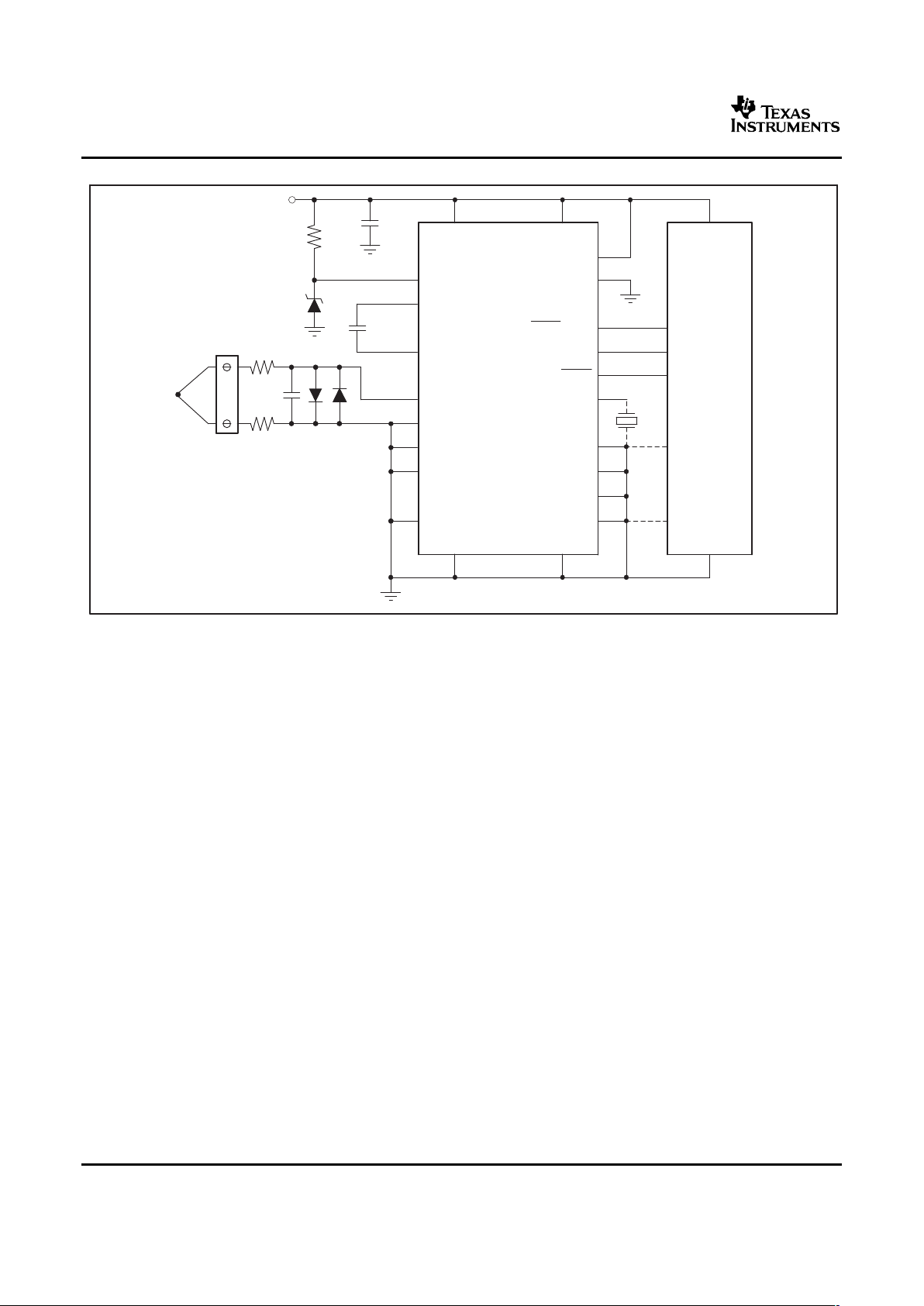
Figure 32 shows a typical ADS1232 hook-up as part
With +5V supply voltage, 177,385 noise-free counts
of a weigh-scale system. In this setup, the ADS1232
can be expected from the ADS1232/4 with the
is configured to channel one input with a gain of 128
onboard PGA set to 128.
at a 10SPS data rate. Note that the internal oscillator
is used by grounding the CLKIN/XTAL1 pin. The
user can also apply either a 4.9152MHz crystal
across the CLKIN/XTAL1 and XTAL2 pins, or simply
See Figure 33 for the ADS1232 in a thermocouple
apply a clock to the CLKIN/XTAL1 pin. For a typical
application. In this example, a type k thermocouple is
2mV/V load cell, the maximum output signal is
used; the temperature range is from –260 ° C to
approximately 10mV for a single +5V excitation
+900 ° C when the gain is set to 64 to maximize the
voltage. The ADS1232/4 can achieve 18.4 noise-free
full input range of the ADS1232. R
1
and a
bits at 10SPS when the PGA = 128 (refer to
REF1004-2.5V are used to set the common-mode
Table 1 ). With the extra software filtering/averaging
voltage to 2.5V for ungrounded junction
(typically done by a microprocessor), an extra bit can
thermocouples. With a gain of 128, the ADS1232
be expected.
input has a typical noise of 17nV
RMS
for extremely
high-resolution applications.
If either a wider temperature range application is
required (up to +1350 ° C, for example), or a
Where:
grounded junction thermocouple is used, pin 1 of the
thermocouple can be grounded (see Figure 34 ).
BIT
EFF
= effective noise-free bits (18.4 + 1 bit
When the gain is set to 2, the ADS1232 input has a
from software filtering/averaging)
typical 500nV offset error and a noise level of
FS
LC
= full-scale output of the load cell (10mV)
270nV
RMS
, which is good for all kinds of low-voltage
FS
AD
= full-scale input of the ADS1232/4 (39mV
output sensors. Note that to calculate the actual
when PGA = 128)
thermocouple temperature, the ADS1232 internal
temperature sensor can be accessed in order to
measure the cold junction temperature along with the
thermocouple reading.
22

www.ti.com
ADS1232
16
9
10
11
12
14
13
15
20
19
24
23
22
4
3
21
8
7
REFP
CAP
CAP
AINP1
AINN1
AINP2
AINN2
REFN
GAIN0
AVDD DVDD
AGND DGND
DRDY/DOUT
SCLK
PDWN
XTAL2
CLKIN/XTAL1
SPEED
A0
TEMP
0.1µF
0.1µF
2.7V to 5.3V
GAIN1
+
−
17 2, 5, 6
18 1
MSP430x4xx
or Other
Microprocessor
VDD
GND
Gain = 128
ADS1232
16
9
10
11
12
14
13
15
20
19
24
23
22
4
3
21
8
7
REFP
CAP
CAP
AINP1
AINN1
AINP2
AINN2
REFN
GAIN0
AVDD DVDD
AGND DGND
DRDY/DOUT
SCLK
PDWN
XTAL2
CLKIN/XTAL1
SPEED
A0
TEMP
0.1µF
0.1µF
2.7V to 5.3V
GAIN1
17 2, 5, 6
18 1
MSP430x4xx
or Other
Microprocessor
VDD
GND
Gain = 128
R
1
50k
Ω
REF1004−2.5V
2
1
Thermocouple Type k
ADS1232
ADS1234
SBAS350C – JUNE 2005 – REVISED JUNE 2006
Figure 32. Weigh Scale Application
Figure 33. Ungrounded Junction Thermocouple Application
23
www.ti.com
ADS1232
16
9
10
11
12
14
13
15
19
20
24
23
22
4
3
21
8
7
REFP
CAP
CAP
AINP1
AINN1
AINP2
AINN2
REFN
GAIN1
AVDD DVDD
AGND DGND
DRDY/DOUT
SCLK
PDWN
XTAL2
CLKIN/XTAL1
SPEED
A0
TEMP
0.1µF
0.1µF
2.7V to 5.3V
GAIN0
17 2, 5, 6
18 1
MSP430x4xx
or Other
Microprocessor
VDD
GND
Gain = 2
R
1
50k
Ω
REF1004−2.5V
2
1
Thermocouple Type k
ADS1232
ADS1234
SBAS350C – JUNE 2005 – REVISED JUNE 2006
Figure 34. Grounded Junction Thermocouple Application
24

www.ti.com
RTDs and Thermistors
ADS1232
16
9
10
14
11
13
12
15
20
19
24
23
22
4
3
21
8
7
REFP
CAP
CAP
AINP2
AINP1
AINN2
AINN1
REFN
GAIN0
AVDD DVDD
AGND DGND
DRDY/DOUT
SCLK
PDWN
XTAL2
CLKIN/XTAL1
SPEED
A0
TEMP
0.1µF
0.1µF
2.7V to 5.3V
GAIN1
17 2, 5, 6
18 1
MSP430x4xx
or Other
Microprocessor
VDD
GND
Gain = 128
R
1
33k
Ω
R
2
33k
Ω
R
L
R
L
R
L
RTD
NOTE: RLis lead resistance.
ADS1232
ADS1234
SBAS350C – JUNE 2005 – REVISED JUNE 2006
common-mode voltage of the ADS1232 PGA. By
using both differential channels of the ADS1232, the
Figure 35 shows a typical schematic for a style 2
temperature change in lead resistance, RL, can be
(three-wire) RTD application. R
1
and R
2
are used to
eliminated. This condition is accomplished by using
excite the RTD as well as establish the
the following formula:
(AINP1 – AINN1) – 2(AINP2 – AINN2).
Figure 35. Style 2 (Three-Wire) RTD Schematic
25
www.ti.com
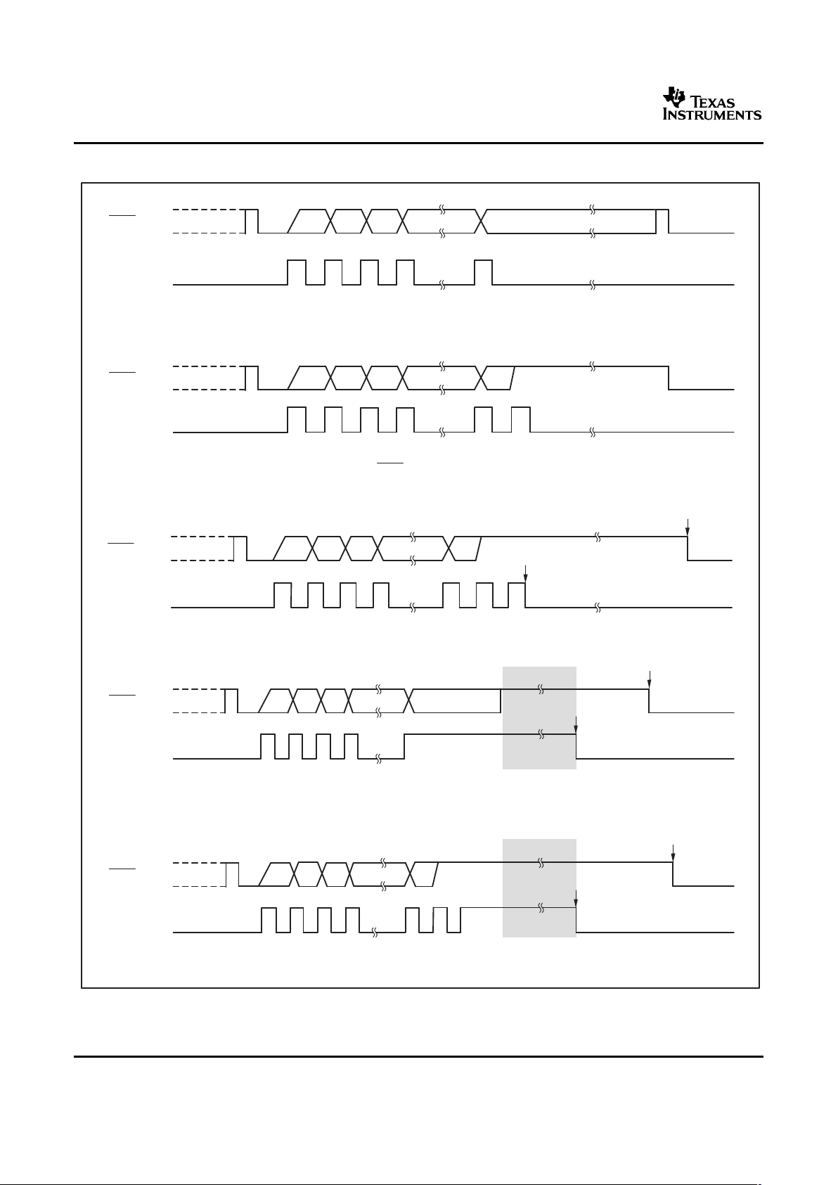
SUMMARY OF SERIAL INTERFACE WAVEFORMS
DRDY/DOUT
SCLK
23 22 21 0
MSB LSB
1 24
DRDY/DOUT
SCLK
23 22 21 0
1 24 25
DRDY/DOUT
SCLK
23 22 21 0
1 24 25 26
Calibration Begins
Data Ready
After Calibration
DRDY/DOUT
SCLK
Data Ready
Start
Conversion
Standby Mode
23 22 21 0
1 24
DRDY/DOUT
SCLK
23 22 21 0
1 24 25
Data Ready
After Calibration
Calibration Begins
(a) Data Retrieval
(b) Data Retrieval with DRDY/DOUT Forced High Afterwards
(c) Offset−Calibration Timing
(d) Standby Mode/Single Conversions
(e) Standby Mode/Single Conversions with Offset Calibration
Standby Mode
ADS1232
ADS1234
SBAS350C – JUNE 2005 – REVISED JUNE 2006
Figure 36. Summary of Serial Interface Waveforms
26

www.ti.com
ADS1232
ADS1234
SBAS350C – JUNE 2005 – REVISED JUNE 2006
Changes from B Revision (September 2005) to C Revision ......................................................................................... Page
• Deleted last row from Absolute Maximum Ratings table. ..................................................................................................... 2
• Changed Analog Inputs section of Electrical Characteristics table. ..................................................................................... 3
• Changed the typical value in last row of Voltage Reference Input section of Electrical Characteristics table. .................... 3
• Added footnote 1 to Table 1 , Table 2 , Table 3 , and Table 4 . ............................................................................................... 5
• Changed fourth sentence in Temperature Sensor section of Overview . ............................................................................ 11
• Added fifth and sixth sentences to Temperature Sensor section of Overview . .................................................................. 11
• Added fourth and fifth sentences to Low-Noise PGA section of Overview ......................................................................... 12
• Changed Figure 19 . ............................................................................................................................................................ 12
• Changed t11to t10in third paragraph of Standby Mode section of Overview . .................................................................... 19
• Changed min and max variables of t10row in table below Figure 29 . ................................................................................ 19
• Changed Figure 31 . ............................................................................................................................................................ 21
• Added last row and second footnote to table below Figure 31 . ......................................................................................... 21
27

PACKAGING INFORMATION
Orderable Device Status
(1)
Package
Type
Package
Drawing
Pins Package
Qty
Eco Plan
(2)
Lead/Ball Finish MSL Peak Temp
(3)
ADS1232IPW ACTIVE TSSOP PW 24 60 Green (RoHS &
no Sb/Br)
CU NIPDAU Level-2-260C-1 YEAR
ADS1232IPWG4 ACTIVE TSSOP PW 24 60 Green (RoHS &
no Sb/Br)
CU NIPDAU Level-2-260C-1 YEAR
ADS1232IPWR ACTIVE TSSOP PW 24 2000 Green (RoHS &
no Sb/Br)
CU NIPDAU Level-2-260C-1 YEAR
ADS1232IPWRG4 ACTIVE TSSOP PW 24 2000 Green (RoHS &
no Sb/Br)
CU NIPDAU Level-2-260C-1 YEAR
ADS1234IPW ACTIVE TSSOP PW 28 50 Green (RoHS &
no Sb/Br)
CU NIPDAU Level-2-260C-1 YEAR
ADS1234IPWG4 ACTIVE TSSOP PW 28 50 Green (RoHS &
no Sb/Br)
CU NIPDAU Level-2-260C-1 YEAR
ADS1234IPWR ACTIVE TSSOP PW 28 2000 Green (RoHS &
no Sb/Br)
CU NIPDAU Level-2-260C-1 YEAR
ADS1234IPWRG4 ACTIVE TSSOP PW 28 2000 Green (RoHS &
no Sb/Br)
CU NIPDAU Level-2-260C-1 YEAR
(1)
The marketing status values are defined as follows:
ACTIVE: Product device recommended for new designs.
LIFEBUY: TI has announced that the device will be discontinued, and a lifetime-buy period is in effect.
NRND: Not recommended for new designs. Device is in production to support existing customers, but TI does not recommend using this part in
a new design.
PREVIEW: Device has been announced but is not in production. Samples may or may not be available.
OBSOLETE: TI has discontinued the production of the device.
(2)
Eco Plan - The planned eco-friendly classification: Pb-Free (RoHS), Pb-Free (RoHS Exempt), or Green (RoHS & no Sb/Br) - please check
http://www.ti.com/productcontent for the latest availability information and additional product content details.
TBD: The Pb-Free/Green conversion plan has not been defined.
Pb-Free (RoHS): TI's terms "Lead-Free" or "Pb-Free" mean semiconductor products that are compatible with the current RoHS requirements
for all 6 substances, including the requirement that lead not exceed 0.1% by weight in homogeneous materials. Where designed to be soldered
at high temperatures, TI Pb-Free products are suitable for use in specified lead-free processes.
Pb-Free (RoHS Exempt): This component has a RoHS exemption for either 1) lead-based flip-chip solder bumps used between the die and
package, or 2) lead-based die adhesive used between the die and leadframe. The component is otherwise considered Pb-Free (RoHS
compatible) as defined above.
Green (RoHS & no Sb/Br): TI defines "Green" to mean Pb-Free (RoHS compatible), and free of Bromine (Br) and Antimony (Sb) based flame
retardants (Br or Sb do not exceed 0.1% by weight in homogeneous material)
(3)
MSL, Peak Temp. -- The Moisture Sensitivity Level rating according to the JEDEC industry standard classifications, and peak solder
temperature.
Important Information and Disclaimer:The information provided on this page represents TI's knowledge and belief as of the date that it is
provided. TI bases its knowledge and belief on information provided by third parties, and makes no representation or warranty as to the
accuracy of such information. Efforts are underway to better integrate information from third parties. TI has taken and continues to take
reasonable steps to provide representative and accurate information but may not have conducted destructive testing or chemical analysis on
incoming materials and chemicals. TI and TI suppliers consider certain information to be proprietary, and thus CAS numbers and other limited
information may not be available for release.
In no event shall TI's liability arising out of such information exceed the total purchase price of the TI part(s) at issue in this document sold by TI
to Customer on an annual basis.
PACKAGE OPTION ADDENDUM
www.ti.com
6-Dec-2006
Addendum-Page 1

MECHANICAL DATA
MTSS001C – JANUARY 1995 – REVISED FEBRUARY 1999
POST OFFICE BOX 655303 • DALLAS, TEXAS 75265
PW (R-PDSO-G**) PLASTIC SMALL-OUTLINE PACKAGE
14 PINS SHOWN
0,65
M
0,10
0,10
0,25
0,50
0,75
0,15 NOM
Gage Plane
28
9,80
9,60
24
7,90
7,70
2016
6,60
6,40
4040064/F 01/97
0,30
6,60
6,20
8
0,19
4,30
4,50
7
0,15
14
A
1
1,20 MAX
14
5,10
4,90
8
3,10
2,90
A MAX
A MIN
DIM
PINS **
0,05
4,90
5,10
Seating Plane
0°–8°
NOTES: A. All linear dimensions are in millimeters.
B. This drawing is subject to change without notice.
C. Body dimensions do not include mold flash or protrusion not to exceed 0,15.
D. Falls within JEDEC MO-153

IMPORTANT NOTICE
Texas Instruments Incorporated and its subsidiaries (TI) reserve the right to make corrections, modifications, enhancements,
improvements, and other changes to its products and services at any time and to discontinue any product or service without notice.
Customers should obtain the latest relevant information before placing orders and should verify that such information is current and
complete. All products are sold subject to TI’s terms and conditions of sale supplied at the time of order acknowledgment.
TI warrants performance of its hardware products to the specifications applicable at the time of sale in accordance with TI’s
standard warranty. Testing and other quality control techniques are used to the extent TI deems necessary to support this
warranty. Except where mandated by government requirements, testing of all parameters of each product is not necessarily
performed.
TI assumes no liability for applications assistance or customer product design. Customers are responsible for their products and
applications using TI components. To minimize the risks associated with customer products and applications, customers should
provide adequate design and operating safeguards.
TI does not warrant or represent that any license, either express or implied, is granted under any TI patent right, copyright, mask
work right, or other TI intellectual property right relating to any combination, machine, or process in which TI products or services
are used. Information published by TI regarding third-party products or services does not constitute a license from TI to use such
products or services or a warranty or endorsement thereof. Use of such information may require a license from a third party under
the patents or other intellectual property of the third party, or a license from TI under the patents or other intellectual property of TI.
Reproduction of TI information in TI data books or data sheets is permissible only if reproduction is without alteration and is
accompanied by all associated warranties, conditions, limitations, and notices. Reproduction of this information with alteration is an
unfair and deceptive business practice. TI is not responsible or liable for such altered documentation. Information of third parties
may be subject to additional restrictions.
Resale of TI products or services with statements different from or beyond the parameters stated by TI for that product or service
voids all express and any implied warranties for the associated TI product or service and is an unfair and deceptive business
practice. TI is not responsible or liable for any such statements.
TI products are not authorized for use in safety-critical applications (such as life support) where a failure of the TI product would
reasonably be expected to cause severe personal injury or death, unless officers of the parties have executed an agreement
specifically governing such use. Buyers represent that they have all necessary expertise in the safety and regulatory ramifications
of their applications, and acknowledge and agree that they are solely responsible for all legal, regulatory and safety-related
requirements concerning their products and any use of TI products in such safety-critical applications, notwithstanding any
applications-related information or support that may be provided by TI. Further, Buyers must fully indemnify TI and its
representatives against any damages arising out of the use of TI products in such safety-critical applications.
TI products are neither designed nor intended for use in military/aerospace applications or environments unless the TI products are
specifically designated by TI as military-grade or "enhanced plastic." Only products designated by TI as military-grade meet military
specifications. Buyers acknowledge and agree that any such use of TI products which TI has not designated as military-grade is
solely at the Buyer's risk, and that they are solely responsible for compliance with all legal and regulatory requirements in
connection with such use.
TI products are neither designed nor intended for use in automotive applications or environments unless the specific TI products
are designated by TI as compliant with ISO/TS 16949 requirements. Buyers acknowledge and agree that, if they use any
non-designated products in automotive applications, TI will not be responsible for any failure to meet such requirements.
Following are URLs where you can obtain information on other Texas Instruments products and application solutions:
Products Applications
Amplifiers amplifier.ti.com Audio www.ti.com/audio
Data Converters dataconverter.ti.com Automotive www.ti.com/automotive
DSP dsp.ti.com Broadband www.ti.com/broadband
Interface interface.ti.com Digital Control www.ti.com/digitalcontrol
Logic logic.ti.com Military www.ti.com/military
Power Mgmt power.ti.com Optical Networking www.ti.com/opticalnetwork
Microcontrollers microcontroller.ti.com Security www.ti.com/security
RFID www.ti-rfid.com Telephony www.ti.com/telephony
Low Power www.ti.com/lpw Video & Imaging www.ti.com/video
Wireless
Wireless www.ti.com/wireless
Mailing Address: Texas Instruments, Post Office Box 655303, Dallas, Texas 75265
Copyright © 2007, Texas Instruments Incorporated
 Loading...