

Page 1
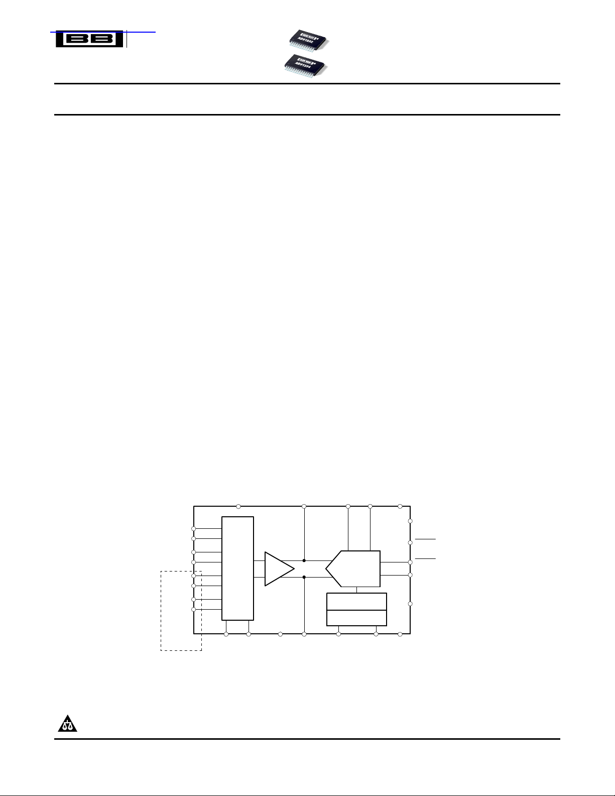
Input
Mux
∆Σ
ADC
REFP REFN
PGA
A = 1, 2, 64,
128
CAP DVDD
DGND
AGNDA1/TEMP
(1)
A0
NOTE: (1) A1 for ADS1234, TEMP for ADS1232.
AINP1
AINN1
AINP2
AINN2
AINP3
AINN3
AINP4
AINN4
ADS1234 Only
SCLK
SPEED
DRDY/DOUT
PDWN
GAIN [1:0]
AVDD
CAP
External Oscillator
Internal Oscillator
XTAL1/CLKIN XTAL2
查询ADS1232供应商查询ADS1232供应商
Ultra Low-Noise, 24-Bit Analog-to-Digital Converter
FEATURES DESCRIPTION
• Up to 23.5 Effective Bits
• RMS Noise:
– 17nV at 10Hz
– 44nV at 80Hz
• On-Board Low Noise Gain-Amp ± 19.5mV with a +5V reference. While the ADS1232
• 19.2-Bit Noise-Free Resolution at Gain = 64
• Simultaneous 50Hz and 60Hz Rejection:
– Internal Clock: 110 dB
– External Clock: 130 dB
• ± 1% Low-Drift On-Board Oscillator
• Selectable Gains of 1, 2, 64, and 128
• Selectable 10/80SPS Conversion Rates
• 2-Channel Differential Input with Built-In Temp
sensor (ADS1232)
• 4-Channel Differential Input (ADS1234)
• External Reference up to AVDD
• Simple Serial Digital Interface
• Supply Range: 2.7V to 5.3V
• –40 ° C to +105 ° C Temperature Range
The ADS1232 and ADS1234 are precision
analog-to-digital (A/D) converters featuring true 23.5
effective-bit performance and exceptional ease of
use. Selectable gains of 1, 2, 64, or 128 allow
full-scale differential input ranges of ± 2.5V to
offers a two-channel differential input and a built-in
temperature sensor, the ADS1234 features a
four-channel differential input multiplexer. A very
low-noise Gain-Amp features low differential input
current to minimize errors when using
high-impedance transducers. An on-board oscillator
is provided for excellent 50Hz and 60Hz rejection
without an external clock source. The devices also
feature a low current driver to accommodate an
external crystal; they also accept external clock
sources for all applications.
All of the features of the ADS1232/ADS1234 are
hard-wire selected, without software programming.
Data is accessed over a simple serial interface
compatible with popular microcontrollers such as the
MSP430. The ADS1232 is available in the 24-pin
TSSOP package, and the ADS1234 is available in
the 28-pin TSSOP.
ADS1232
ADS1234
SBAS350 – JUNE 2005
APPLICATIONS
• Weigh Scales
• Strain Gauges
• Bridge Sensors
• Industrial Process Control
PRODUCT PREVIEW information concerns products in the formative or design phase of development. Characteristic data and other
specifications are design goals. Texas Instruments reserves the
right to change or discontinue these products without notice.
Please be aware that an important notice concerning availability, standard warranty, and use in critical applications of Texas
Instruments semiconductor products and disclaimers thereto appears at the end of this data sheet.
Copyright © 2005, Texas Instruments Incorporated
Page 2
www.ti.com
PRODUCT PREVIEW
ADS1232
ADS1234
SBAS350 – JUNE 2005
This integrated circuit can be damaged by ESD. Texas Instruments recommends that all integrated
circuits be handled with appropriate precautions. Failure to observe proper handling and installation
procedures can cause damage.
ESD damage can range from subtle performance degradation to complete device failure. Precision
integrated circuits may be more susceptible to damage because very small parametric changes could
cause the device not to meet its published specifications.
ORDERING INFORMATION
PRODUCT PACKAGE-LEAD TEMPERATURE
ADS1232 TSSOP-24 PW –40°C to 105°C ADS1232
ADS1234 TSSOP-28 PW –40°C to 105°C ADS1234
(1) For the most current package and ordering information, see the Package Option Addendum at the end of this document, or see the TI
website at www.ti.com.
PACKAGE PACKAGE ORDERING TRANSPORT MEDIA,
DESIGNATOR MARKING NUMBER QUANTITY
SPECIFIED
RANGE
(1)
ADS1232IPWT Tape and Reel, 250
ADS1232IPWR Tape and Reel, 2500
ADS1234IPWT Tape and Reel, 250
ADS1234IPWR Tape and Reel, 2500
ABSOLUTE MAXIMUM RATINGS
over operating free-air temperature range (unless otherwise noted)
AVDD to AGND –0.3 to +6 V
DVDD to DGND –0.3 to +6 V
AGND to DGND –0.3 to +0.3 V
Input Current 100, Momentary mA
Input Current 10, Continuous mA
Analog Input Voltage to AGND –0.3 to AVDD + 0.3 V
Digital Input Voltage to DGND –0.3 to DVDD + 0.3 V
Maximum Junction Temperature +150 °C
Operating Temperature Range –40 to +105 °C
Storage Temperature Range –60 to +150 °C
Lead Temperature (soldering, 10s) +300 °C
(1) Stresses beyond those listed under Absolute Maximum Ratings may cause permanent damage to the device. These are stress ratings
only, and functional operation of the device at these or any other conditions beyond those indicated under Recommended Operating
Conditions is not implied. Exposure to absolute-maximum-rated conditions for extended periods may affect device reliability.
(1)
ADS1232, ADS1234 UNIT
2
Page 3
www.ti.com
ADS1232
ADS1234
SBAS350 – JUNE 2005
ELECTRICAL CHARACTERISTICS: V
= +5V
REF
All specifications TA= –40°C to +105°C, AVDD = DVDD = VREFP = +5V, VREFN = AGND, Internal Oscillator, SPEED =
Low, Gain = 64 (unless otherwise specified).
ADS1232, ADS1234
PARAMETER CONDITIONS MIN TYP MAX UNIT
Analog Inputs
Full-Scale Input Voltage
(AIN
- AIN
)
P
N
Common-mode Input Range
AINxP or AINxN
with respect to GND, Gain = 1
AGND – 0.1 AVDD + 0.1 V
Gain = 64, 128 (0.5)AVDD – 1 (0.5)AVDD + 1 V
Differential Input Current
Gain = 1, 2 500 nA
Gain = 64, 128 50 nA
System Performance
Resolution No missing codes 24 Bits
Internal Oscillator, SPEED = High TBD 80 TBD SPS
Conversion Rate
Internal Oscillator, SPEED = Low TBD 10 TBD SPS
External Oscillator, SPEED = High f
External Oscillator, SPEED = Low f
Digital Filter Settling Time Full Settling 4 Conversions
Differential input, End point fit
Integral Non-Linearity (INL)
Gain = 1, 2
Differential input, End point fit
Gain = 64, 128
Input Offset Error
Input Offset Error Drift
Gain Error
(3)
Gain Error Drift
(2)
Gain = 1 ± 0.2 TBD ppm of FS
Gain = 64 ± 2 TBD ppm of FS
Gain = 1 1 µV/°C
Gain = 64 15 nV/°C
Gain = 1 0.001 TBD %
Gain = 64 0.001 TBD %
Gain = 1 0.5 ppm/ ° C
Gain = 64 ± 4 ppm/ ° C
Internal oscillator, 50Hz and 60Hz 100 110 dB
Normal-mode Rejection
(4)
External oscillator,
50Hz and 60Hz, ± 1Hz
Common-mode Rejection
at DC, Gain = 1, ∆ VDD = 1V TBD 100 dB
at DC, Gain = 64, ∆ VDD = 0.1V TBD 75 dB
Input-Referred Noise See Noise Performance Tables
Power-Supply Rejection
at DC, Gain = 1, ∆ VDD = 1V TBD 100 dB
at DC, Gain = 64, ∆ VDD = 0.1V TBD 85 dB
Voltage Reference Input
Voltage Reference Input
(V
)
REF
Negative Reference Input
(VREFN)
Positive Reference Input
(VREFP)
V
= VREFP - VREFN 1 AVDD AVDD + 0.1V V
REF
AGND – 0.1 VREFP – 1.0 V
VREFN + 1.0 AVDD + 0.1 V
Voltage Reference
Input Current
(1) FSR = full scale range = V
(2) Offset calibration can minimize these errors to the level of noise at any temperature.
/Gain
REF
(3) Gain errors are calibrated at the factory (AVDD = +5V, all gains, TA= +25 ° C).
(4) Specification is assured by the combination of design and final production test.
±0.5V
/Gain V
REF
/ 61440 SPS
CLK
/ 491520 SPS
CLK
± 0.0002 ± 0.0015 % of FSR
± 0.0010 TBD % of FSR
120 130 dB
50 nA
(1)
3
Page 4

www.ti.com
PRODUCT PREVIEW
ADS1232
ADS1234
SBAS350 – JUNE 2005
ELECTRICAL CHARACTERISTICS: V
= +5V (continued)
REF
All specifications TA= –40°C to +105°C, AVDD = DVDD = VREFP = +5V, VREFN = AGND, Internal Oscillator, SPEED =
Low, Gain = 64 (unless otherwise specified).
ADS1232, ADS1234
PARAMETER CONDITIONS MIN TYP MAX UNIT
Digital
Logic Levels
V
IH
V
IL
V
OH
V
OL
Input Leakage 0 < VIN< DVDD ± 10 µA
Power Supply
Power Supply Voltage
(AVDD, DVDD)
Analog Supply Current
Digital Supply Current
Power Dissipation, Total
IOH= 1mA DVDD – 0.4 V
IOL= 1mA 0.2 DVDD V
Normal mode, AVDD = 3V, Gain = 1, 2 600 TBD µA
Normal mode, AVDD = 3V,
Gain = 64, 128
Normal mode, AVDD = 5V, Gain = 1, 2 700 TBD µA
Normal mode, AVDD = 5V,
Gain = 64, 128
Standby mode 0.1 TBD µA
Power-down 0.1 TBD µA
Normal mode, DVDD = 3V, Gain = 1, 2 90 TBD µA
Normal mode, DVDD = 3V,
Gain = 64, 128
Normal mode, DVDD = 5V, Gain = 1, 2 110 TBD µA
Normal mode, DVDD = 5V,
Gain = 64, 128
Standby mode, SCLK = High 50 TBD µA
Power-down 0.1 TBD µA
Normal mode, AVDD = DVDD = 3V,
Gain = 1, 2
Normal mode, AVDD = DVDD = 5V,
Gain = 1, 2
Normal mode, AVDD = DVDD = 3V,
Gain = 64, 128
Normal mode, AVDD = DVDD = 5V,
Gain = 64, 128
Standby TBD TBD mW
Power-down TBD TBD mW
0.6 DVDD DVDD + 0.1 V
DGND 0.3 DVDD V
2.7 5.3 V
1500 TBD µA
1600 TBD µA
90 TBD µA
110 TBD µA
2.1 TBD mW
4 TBD mW
4.8 TBD mW
8.6 TBD mW
4
Page 5

www.ti.com
DVDD
DGND
XTAL1/CLKIN
XTAL2
DGND
DGND
A1
A0
CAP
CAP
AINP1
AINN1
AINP3
AINN3
DRDY/DOUT
SCLK
PDWN
SPEED
GAIN1
GAIN0
AVDD
AGND
REFP
REFN
AINP2
AINN2
AINP4
AINN4
1
2
3
4
5
6
7
8
9
10
11
12
13
14
28
27
26
25
24
23
22
21
20
19
18
17
16
15
ADS1234
DVDD
DGND
XTAL1/CLKIN
XTAL2
DGND
DGND
TEMP
A0
CAP
CAP
AINP1
AINN1
DRDY/DOUT
SCLK
PDWN
SPEED
GAIN1
GAIN0
AVDD
AGND
REFP
REFN
AINP2
AINN2
1
2
3
4
5
6
7
8
9
10
11
12
24
23
22
21
20
19
18
17
16
15
14
13
ADS1232
ADS1232
ADS1234
SBAS350 – JUNE 2005
DEVICE INFORMATION
5
Page 6

www.ti.com
PRODUCT PREVIEW
ADS1232
ADS1234
SBAS350 – JUNE 2005
DEVICE INFORMATION (continued)
TERMINAL
NAME ADS1232 ADS1234 INPUT/OUTPUT DESCRIPTION
DVDD 1 1 Digital Digital Power Supply: 2.7V to 5.3V
DGND 2 2 Digital Digital Ground
XTAL1/ External Clock Input: Typically 4.9152MHz. Ties low to activate Internal Oscillator. Can also use
CLKIN external Crystal Oscillator across XTAL1/CLKIN and XTAL2 pins. See text for more details.
XTAL2 4 4 Digital External Clock Output pin. See text for more details.
DGND 5 5 Digital Digital Ground
DGND 6 6 Digital Digital Ground
TEMP 7 – Digital Input Onboard Temperature Diode Enable Input pin
A1 – 7 Digital Input Input Mux Select Input pin (MSB)
A0 8 8 Digital Input Input Mux Select Input pin (LSB):
CAP 9 9 Analog Gain Amp Bypass Capacitor Connection
CAP 10 10 Analog Gain Amp Bypass Capacitor Connection
AINP1 11 11 Digital Input Positive Analog Input Channel 1
AINN1 12 12 Digital Input Negative Analog Input Channel 1
AINP3 – 13 Digital Input Positive Analog Input Channel 3
AINN3 – 14 Digital Input Negative Analog Input Channel 3
AINN4 – 15 Digital Input Negative Analog Input Channel 4
AINP4 – 16 Digital Input Positive Analog Input Channel 4
AINN2 13 17 Digital Input Negative Analog Input Channel 2
AINP2 14 18 Digital Input Positive Analog Input Channel 2
REFN 15 19 Digital Input Negative Reference Input pin
REFP 16 20 Digital Input Positive Reference Input pin
AGND 17 21 Analog Analog Ground
AVDD 18 22 Analog Analog Power Supply, 2.7V to 5.3V
GAIN0 19 23 Digital Input Gain Select Input pin (LSB)
GAIN1 20 24 Digital Input Gain Select Input pin (MSB):
SPEED 21 25 Digital Input Output Data Rate Select Input pin:
3 3 Digital/Digital Input
PDWN 22 26 Digital Input
SCLK 23 27 Digital Input
DRDY/
DOUT
24 28 Digital Input Dual-Purpose Output:
PIN DESCRIPTIONS
ANALOG/DIGITAL
A1 A0 Channel
0 0 AIN1
0 1 AIN2
1 0 AIN3
1 1 AIN4
GAIN1 GAIN0 PGA
0 0 1
0 1 2
1 0 64
1 1 128
SPEED DATA RATE
0 10Hz
1 80Hz
Power Down Input pin: Holding this pin low powers down the entire converter and resets the A/D
converter.
Serial Clock Input pin: Clock out data on the rising edge. Used to initiate Offset Calibration and
Sleep modes. See text for more details.
Data Ready: Indicates valid data by going low.
Data Output: Outputs data, MSB first, on the first rising edge of SCLK.
6
Page 7

www.ti.com
ADS1232
ADS1234
SBAS350 – JUNE 2005
NOISE PERFORMANCE
The ADS1232/1234 offer outstanding noise performance that can be optimized for a givven full-scale range using
the on-chip programmable gain amplifier, Table 1 , Table 2 , Table 3 , and Table 4 summarize the typical noise
performance with inputs shorted externally for different gains, data rates and voltage reference values.
The RMS and Peak-to-Peak noise are referred to the input. The Effective Number of Bits (ENOB) is defined as:
• ENOB = ln (FSR/RMS noise)/ln(2)
The Noise Free Bits are defined as:
• Noise-Free Bits = ln (FSR/Peak-to-Peak Noise)/ln(2)
Where FSR (Full-Scale Range) = V
/Gain
REF
Table 1. AVDD = 5V, V
GAIN RMS NOISE PEAK-TO-PEAK NOISE ENOB (rms) NOISE-FREE BITS
1 420nV 1.79µV 23.5 21.4
2 270nV 900nV 23.1 21.4
64 19nV 125nV 22.0 19.2
128 17nV 110nV 21.1 18.4
Table 2. AVDD = 5V, V
GAIN RMS NOISE PEAK-TO-PEAK NOISE ENOB (rms) NOISE-FREE BITS
1 1.36µV 8.3µV 21.8 19.2
2 850nV 5.5µV 21.5 18.8
64 48nV 307nV 20.6 18
128 44nV 247nV 19.7 17.2
Table 3. AVDD = 3V, V
GAIN RMS NOISE PEAK-TO-PEAK NOISE ENOB (rms) NOISE-FREE BITS
1 450nV 2.8µV 22.6 20
2 325nV 1.8µV 22.1 19.7
64 20nV 130nV 21.2 18.5
128 18nV 115nV 20.3 17.6
Table 4. AVDD = 3V, V
GAIN RMS NOISE PEAK-TO-PEAK NOISE ENOB (rms) NOISE-FREE BITS
1 2.2µV 12µV 20.4 17.9
2 1.2µV 6.8µV 20.2 17.8
64 54nV 340nV 19.7 17.1
128 48nV 254nV 18.9 16.5
= 5V, Data Rate = 10SPS
REF
= 5V, Data Rate = 80SPS
REF
= 3V, Data Rate = 10SPS
REF
= 3V, Data Rate = 80SPS
REF
7
Page 8

PACKAGE OPTION ADDENDUM
www.ti.com
29-Jun-2005
PACKAGING INFORMATION
Orderable Device Status
(1)
Package
Type
Package
Drawing
Pins Package
Qty
Eco Plan
ADS1232IPW PREVIEW TSSOP PW 24 60 TBD Call TI Call TI
ADS1232IPWR PREVIEW TSSOP PW 24 2000 TBD Call TI Call TI
ADS1234IPW PREVIEW TSSOP PW 28 50 TBD Call TI Call TI
ADS1234IPWR PREVIEW TSSOP PW 28 2000 TBD Call TI Call TI
(1)
The marketing status values are defined as follows:
ACTIVE: Product device recommended for new designs.
LIFEBUY: TI has announced that the device will be discontinued, and a lifetime-buy period is in effect.
NRND: Not recommended for new designs. Device is in production to support existing customers, but TI does not recommend using this part in
a new design.
PREVIEW: Device has been announced but is not in production. Samples may or may not be available.
OBSOLETE: TI has discontinued the production of the device.
(2)
Eco Plan - The planned eco-friendly classification: Pb-Free (RoHS) or Green (RoHS & no Sb/Br) - please check
http://www.ti.com/productcontent for the latest availability information and additional product content details.
TBD: The Pb-Free/Green conversion plan has not been defined.
Pb-Free (RoHS): TI's terms "Lead-Free" or "Pb-Free" mean semiconductor products that are compatible with the current RoHS requirements
for all 6 substances, including the requirement that lead not exceed 0.1% by weight in homogeneous materials. Where designed to be soldered
at high temperatures, TI Pb-Free products are suitable for use in specified lead-free processes.
Green (RoHS & no Sb/Br): TI defines "Green" to mean Pb-Free (RoHS compatible), and free of Bromine (Br) and Antimony (Sb) based flame
retardants (Br or Sb do not exceed 0.1% by weight in homogeneous material)
(2)
Lead/Ball Finish MSL Peak Temp
(3)
(3)
MSL, Peak Temp. -- The Moisture Sensitivity Level rating according to the JEDEC industry standard classifications, and peak solder
temperature.
Important Information and Disclaimer:The information provided on this page represents TI's knowledge and belief as of the date that it is
provided. TI bases its knowledge and belief on information provided by third parties, and makes no representation or warranty as to the
accuracy of such information. Efforts are underway to better integrate information from third parties. TI has taken and continues to take
reasonable steps to provide representative and accurate information but may not have conducted destructive testing or chemical analysis on
incoming materials and chemicals. TI and TI suppliers consider certain information to be proprietary, and thus CAS numbers and other limited
information may not be available for release.
In no event shall TI's liability arising out of such information exceed the total purchase price of the TI part(s) at issue in this document sold by TI
to Customer on an annual basis.
Addendum-Page 1
Page 9

MECHANICAL DATA
MTSS001C – JANUARY 1995 – REVISED FEBRUARY 1999
PW (R-PDSO-G**) PLASTIC SMALL-OUTLINE PACKAGE
14 PINS SHOWN
0,65
1,20 MAX
14
0,30
0,19
8
4,50
4,30
PINS **
7
Seating Plane
0,15
0,05
8
1
A
DIM
14
0,10
6,60
6,20
M
0,10
0,15 NOM
0°–8°
2016
Gage Plane
24
0,25
0,75
0,50
28
A MAX
A MIN
NOTES: A. All linear dimensions are in millimeters.
B. This drawing is subject to change without notice.
C. Body dimensions do not include mold flash or protrusion not to exceed 0,15.
D. Falls within JEDEC MO-153
3,10
2,90
5,10
4,90
5,10
4,90
6,60
6,40
7,90
7,70
9,80
9,60
4040064/F 01/97
POST OFFICE BOX 655303 • DALLAS, TEXAS 75265
Page 10

IMPORTANT NOTICE
Texas Instruments Incorporated and its subsidiaries (TI) reserve the right to make corrections, modifications,
enhancements, improvements, and other changes to its products and services at any time and to discontinue
any product or service without notice. Customers should obtain the latest relevant information before placing
orders and should verify that such information is current and complete. All products are sold subject to TI’s terms
and conditions of sale supplied at the time of order acknowledgment.
TI warrants performance of its hardware products to the specifications applicable at the time of sale in
accordance with TI’s standard warranty. Testing and other quality control techniques are used to the extent TI
deems necessary to support this warranty . Except where mandated by government requirements, testing of all
parameters of each product is not necessarily performed.
TI assumes no liability for applications assistance or customer product design. Customers are responsible for
their products and applications using TI components. To minimize the risks associated with customer products
and applications, customers should provide adequate design and operating safeguards.
TI does not warrant or represent that any license, either express or implied, is granted under any TI patent right,
copyright, mask work right, or other TI intellectual property right relating to any combination, machine, or process
in which TI products or services are used. Information published by TI regarding third-party products or services
does not constitute a license from TI to use such products or services or a warranty or endorsement thereof.
Use of such information may require a license from a third party under the patents or other intellectual property
of the third party, or a license from TI under the patents or other intellectual property of TI.
Reproduction of information in TI data books or data sheets is permissible only if reproduction is without
alteration and is accompanied by all associated warranties, conditions, limitations, and notices. Reproduction
of this information with alteration is an unfair and deceptive business practice. TI is not responsible or liable for
such altered documentation.
Resale of TI products or services with statements different from or beyond the parameters stated by TI for that
product or service voids all express and any implied warranties for the associated TI product or service and
is an unfair and deceptive business practice. TI is not responsible or liable for any such statements.
Following are URLs where you can obtain information on other Texas Instruments products and application
solutions:
Products Applications
Amplifiers amplifier.ti.com Audio www.ti.com/audio
Data Converters dataconverter.ti.com Automotive www.ti.com/automotive
DSP dsp.ti.com Broadband www.ti.com/broadband
Interface interface.ti.com Digital Control www.ti.com/digitalcontrol
Logic logic.ti.com Military www.ti.com/military
Power Mgmt power.ti.com Optical Networking www.ti.com/opticalnetwork
Microcontrollers microcontroller.ti.com Security www.ti.com/security
Telephony www.ti.com/telephony
Video & Imaging www.ti.com/video
Wireless www.ti.com/wireless
Mailing Address: Texas Instruments
Post Office Box 655303 Dallas, Texas 75265
Copyright 2005, Texas Instruments Incorporated
 Loading...