

Page 1
Please be aware that an important notice concerning availability, standard warranty, and use in critical applications of Texas Instruments
查询ADS1224供应商查询ADS1224供应商
SBAS286A − JUNE 2003 − REVISED MARCH 2004
FEATURES
D 240SPS Data Rate with 4MHz Clock
D 20-Bit Effective Resolution
D Input Multiplexer with Four Differential
Channels
D Pin-Selectable, High-Impedance Input Buffer
D ±5V Differential Input Range
D 0.0003% INL (typ), 0.0015% INL (max)
D Self-Calibrating
D Simple 2-Wire Serial Interface
D On-Chip Temperature Sensor
D Single Conversions with Standby Mode
D Low Current Consumption: 300µA
D Analog Supply: 2.7V to 5.5V
D Digital Supply: 2.7V to 5.5V
APPLICATIONS
D Hand-Held Instrumentation
D Portable Medical Equipment
D Industrial Process Control
D Weigh Scales
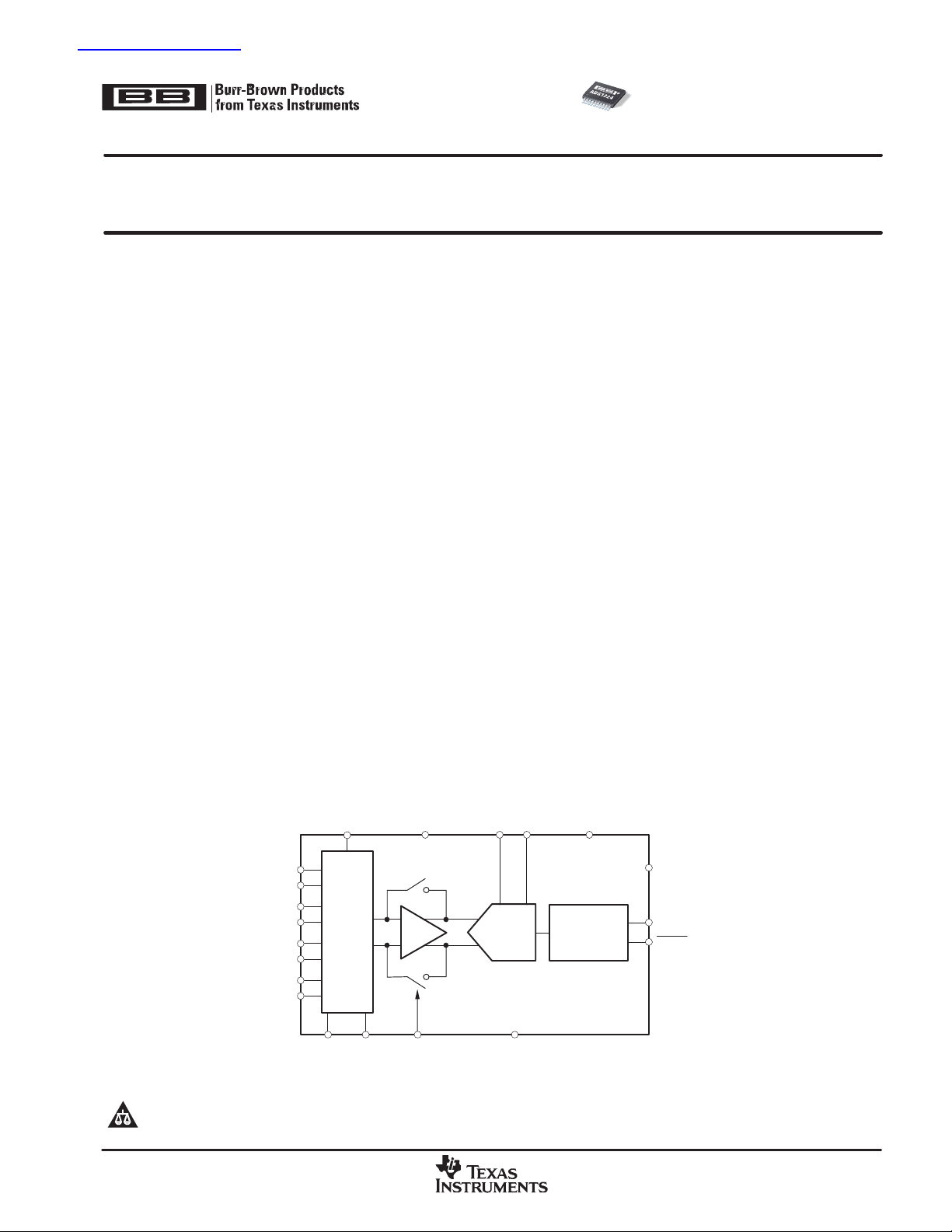
DESCRIPTION
The ADS1224 is a 4-channel, 24-bit, delta-sigma analog-to-digital (A/D) converter. It offers excellent performance and low power in a TSSOP-20 package. The
ADS1224 is well-suited for demanding, high-resolution
measurements, especially in portable systems and other space-saving and power-constrained applications.
A delta-sigma modulator and digital filter form the basis
of the A/D converter. The analog modulator has a ±5V
differential input range. An input multiplexer (mux) is
used to select between four separate differential input
channels. A bu ffer can be selected to increase the input
impedance of the measurement.
A simple, 2-wire serial interface provides all the
necessary control. Data retrieval, self-calibration, and
Standby mode are handled with a few simple
waveforms. When only single conversions are needed,
the ADS1224 can be quickly shut down (Standby mode)
while idle between measurements to dramatically
reduce the overall power consumption. Multiple
ADS1224s can be connected together to create a
synchronously sampling multichannel measurement
system. The ADS1224 is designed to easily connect to
microcontrollers, such as the MSP430.
The ADS1224 supports 2.7V to 5.5V analog supplies
and 2.7V to 5.5V digital supplies. Power is typically less
than 1mW in 3V operation and less than 1µW during
Standby mode.
TEMPEN
AINP1
AINN1
AINP2
AINN2
AINP3
AINN3
AINP4
AINN4
semiconductor products and disclaimers thereto appears at the end of this data sheet.
All trademarks are the property of their respective owners.
!"# " $ % & % '& () (&%
&$ %&&% $% "% %$% %(( *)
(& &%% (% &%%* &( % $%)
Mux
MUX1 BUFEN
AVDD DVDD
Buffer
VREFP VREFN
∆Σ
Modulator
GNDMUX0
www.ti.com
Digital Filter
and
SerialInterface
Copyright 2003−2004, Texas Instruments Incorporated
CLK
SCLK
DRDY/DOUT
Page 2
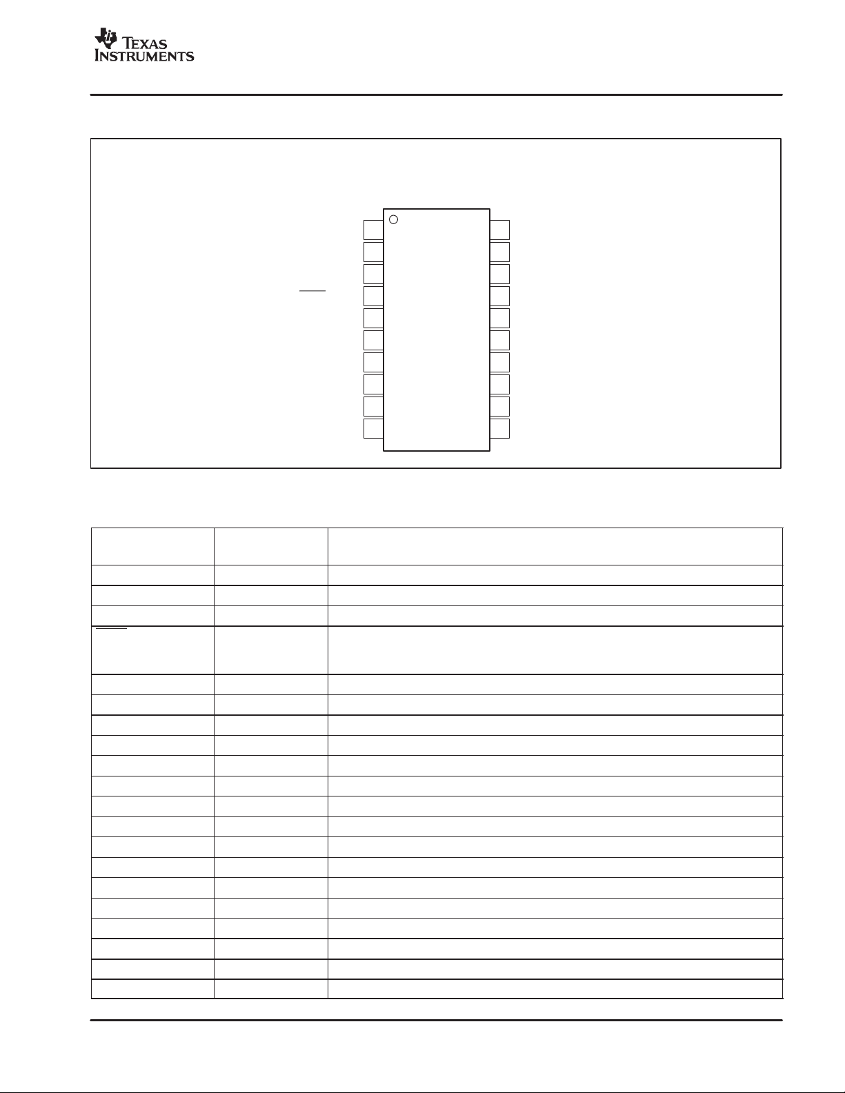
ADS1224
TSSOP-20
PW
−40°C to +85°C
ADS1224
Input current
SBAS286A − JUNE 2003 − REVISED MARCH 2004
ORDERING INFORMATION
PRODUCT PACKAGE−LEAD
(1)
For the most current specification and package information, refer to our web site at www.ti.com.
PACKAGE
DESIGNATOR
(1)
SPECIFIED
TEMPERATURE
RANGE
PACKAGE
MARKING
www.ti.com
ORDERING
NUMBER
ADS1224IPWT Tape and Reel, 250
ADS1224IPWR Tape and Reel, 2500
TRANSPORT
MEDIA, QUANTITY
ABSOLUTE MAXIMUM RATINGS
over operat i n g f ree-air temperature range unless otherwise noted
ADS1224 UNIT
AVDD to GND −0.3 to +6 V
DVDD to GND −0.3 to +6 V
100, momentary mA
10, continuous mA
Analog input voltage to GND −0.3 to AVDD + 0.3 V
Digital input voltage to GND −0.3 to DVDD + 0.3 V
Maximum Junction Temperature +150 °C
Operating Temperature Range −55 to +125 °C
Storage Temperature Range −60 to +150 °C
Lead Tem perature (soldering, 10s) +300 °C
(1)
Stresses above these ratings may cause permanent damage.
Exposure to absolute maximum conditions for extended periods
may degrade device reliability. These are stress ratings only , an d
functional operation of the device at these or any other conditions
beyond those specified is not implied.
(1)
This integrated circuit can be damaged by ESD. Texas
Instruments recommends that all integrated circuits be
handled with appropriate precautions. Failure to observe
proper handling and installation procedures can cause damage.
ESD damage can range from subtle performance degradation to
complete device failure. Precision integrated circuits may be more
susceptible t o damage because very small parametric changes could
cause the device not to meet its published specifications.
2
Page 3
Absolute input voltage
Differential input impedance
Integral nonlinearity (INL)
Offset error
Offset error drift
Gain error
Gain error drift
Common-mode rejection
Analog power-supply rejection
Digital power-supply rejection
www.ti.com
SBAS286A − JUNE 2003 − REVISED MARCH 2004
ELECTRICAL CHARACTERISTICS
All specifications at TA = −40°C to +85°C, AVDD = +5V, DVDD = +5V, f
PARAMETER TEST CONDITIONS MIN TYP MAX UNIT
Analog Input
Full-scale input voltage AINP − AINN ±2V
Buffer off; AINP, AINN with respect to GND GND − 0.1 A VDD + 0.1 V
Buffer on; AINP, AINN with respect to GND GND + 0.05 AVDD − 1.5 V
Buffer off; f
Buffer on; f
Common-mode input impedance Buffer off; f
System Performance
Resolution No missing codes 24 Bits
Data rate 120 (f
Buffer off, Differential input signal, end point fit 0.0003 0.0015 % of FSR
Buffer on, Differential input signal, end point fit 0.0006 % of FSR
Buffer off 20 100 µV
Buffer on 20 µV
Buffer off 0.2 µV/°C
Buffer on 0.2 µV/°C
Offset error match Between channels 20 100 µV
Buffer off 0.004 0.025 %
Buffer on 0.008 %
Buffer off 0.00003 % of FSR/°C
Buffer on 0.00006 % of FSR/°C
Gain error match Between channels 0.0005 %
Buffer off, at DC 90 110 dB
Buffer on, at DC 90 110 dB
Buffer off, at DC, ± 10% ∆ in AVDD 95 dB
Buffer on, at DC, ± 10% ∆ in AVDD 95 dB
Buffer off, at DC, DVDD = 2.7V to 5.5V 85 dB
Buffer on, at DC, DVDD = 2.7V to 5.5V 85 dB
Noise 0.8 ppm of FSR, rms
Temperature Sensor
Temperature sensor voltage TA = 25°C 106 mV
Temperature sensor coefficient 360 µV/°C
Voltage Reference Input
Reference input voltage V
Negative reference input Buffer off GND − 0.1 VREFP − 0.5 V
Positive reference input Buffer off VREFN + 0.5 AV DD + 0.1 V
Negative reference input Buffer on GND + 0.05 VREFP − 0.5 V
Positive reference input Buffer on VREFN + 0.5 AVD D − 1.5 V
Voltage reference impedance f
(1)
SPS = samples per second.
(2)
FSR = full-scale range = 4V
(3)
It will not be possible to reach the digital output full-scale code when V
REF
.
= VREFP − VREFN 0.5 2.5 AVDD
REF
= 2MHz 500 kΩ
CLK
= 2MHz 2.7 MΩ
CLK
= 2MHz 1.2 GΩ
CLK
= 2MHz 5.4 MΩ
CLK
= 2MHz, and V
CLK
> AVDD/2.
REF
= +2.5V , unless otherwise noted.
REF
REF
/2MHz) SPS
CLK
(3)
V
(1)
(2)
V
3
Page 4
Logic
Logic
levels
AVDD current
DVDD current
Total power dissipation
www.ti.com
SBAS286A − JUNE 2003 − REVISED MARCH 2004
ELECTRICAL CHARACTERISTICS (continued)
All specifications at TA = −40°C to +85°C, AVDD = +5V, DVDD = +5V, f
PARAMETER UNITMAXTYPMINTEST CONDITIONS
Digital Input/Output
V
IH
V
IL
levels
Input leakage ±10 µA
CLK frequency (f
CLK duty cycle 30 70 %
Power Supply
AVDD 2.7 5.5 V
DVDD 2.7 5.5 V
AVDD current
DVDD current
Temperature Range
Specified −40 +85 °C
Operating −55 +125 °C
Storage −60 +150 °C
(1)
SPS = samples per second.
(2)
FSR = full-scale range = 4V
(3)
It will not be possible to reach the digital output full-scale code when V
V
OH
V
OL
) 8 MHz
CLK
IOH = 1mA 0.8 DVDD V
IOL = 1mA 0.2 DVDD V
Standby mode < 1 µA
AVDD = 5V, normal mode, buffer off 285 µA
AVDD = 5V, normal mode, buffer on 405 µA
AVDD = 3V, normal mode, buffer off 265 µA
AVDD = 3V, normal mode, buffer on 385 µA
Standby mode < 1 µA
DVDD = 5V , normal mode 20 µA
DVDD = 3V , normal mode 10 µA
AVDD = DVDD = 5V, buffer of f 1.5 2.25 mW
AVDD = DVDD = 3V, buffer of f 0.8 mW
.
REF
= 2MHz, and V
CLK
> AVDD/2.
REF
= +2.5V , unless otherwise noted.
REF
0.8 DVDD DVDD + 0.1 V
GND − 0.1 0.2 DVDD V
4
Page 5
www.ti.com
PIN ASSIGNMENTS
SBAS286A − JUNE 2003 − REVISED MARCH 2004
PW PACKAGE
TSSOP
(TOP VIEW)
DVDD
SCLK
CLK
DRDY/DOUT
MUX0
MUX1
TEMPEN
BUFEN
AINP4
AINN4
10
1
2
3
4
5
6
7
8
9
ADS1224
20
19
18
17
16
15
14
13
12
11
AVDD
VREFP
VREFN
GND
AINN1
AINP1
AINN2
AINP2
AINN3
AINP3
Terminal Functions
TERMINAL
NAME NO. I/O DESCRIPTION
DVDD 1 Digital Digital power supply
SCLK 2 Digital input Serial clock input
CLK 3 Digital input System clock input
DRDY/DOUT 4 Digital Ouput Dual-purpose output:
Data Ready: indicates valid data by going low.
Data Output: outputs data, MSB first, on the rising edge of SCLK.
MUX0 5 Digital input Selects analog input of mux, bit 0
MUX1 6 Digital input Selects analog input of mux, bit 1
TEMPEN 7 Digital input Selects temperature sensor input from mux
BUFEN 8 Digital input Enables input buffer
AINP4 9 Analog input Analog channel 4 positive input
AINN4 10 Analog input Analog channel 4 negative input
AINP3 11 Analog input Analog channel 3 positive input
AINN3 12 Analog input Analog channel 3 negative input
AINP2 13 Analog input Analog channel 2 positive input
AINN2 14 Analog input Analog channel 2 negative input
AINP1 15 Analog input Analog channel 1 positive input
AINN1 16 Analog input Analog channel 1 negative input
GND 17 Analog/Digital Analog and digital ground
VREFN 18 Analog input Negative reference input
VREFP 19 Analog input Positive reference input
AVDD 20 Analog Analog power supply
5
Page 6
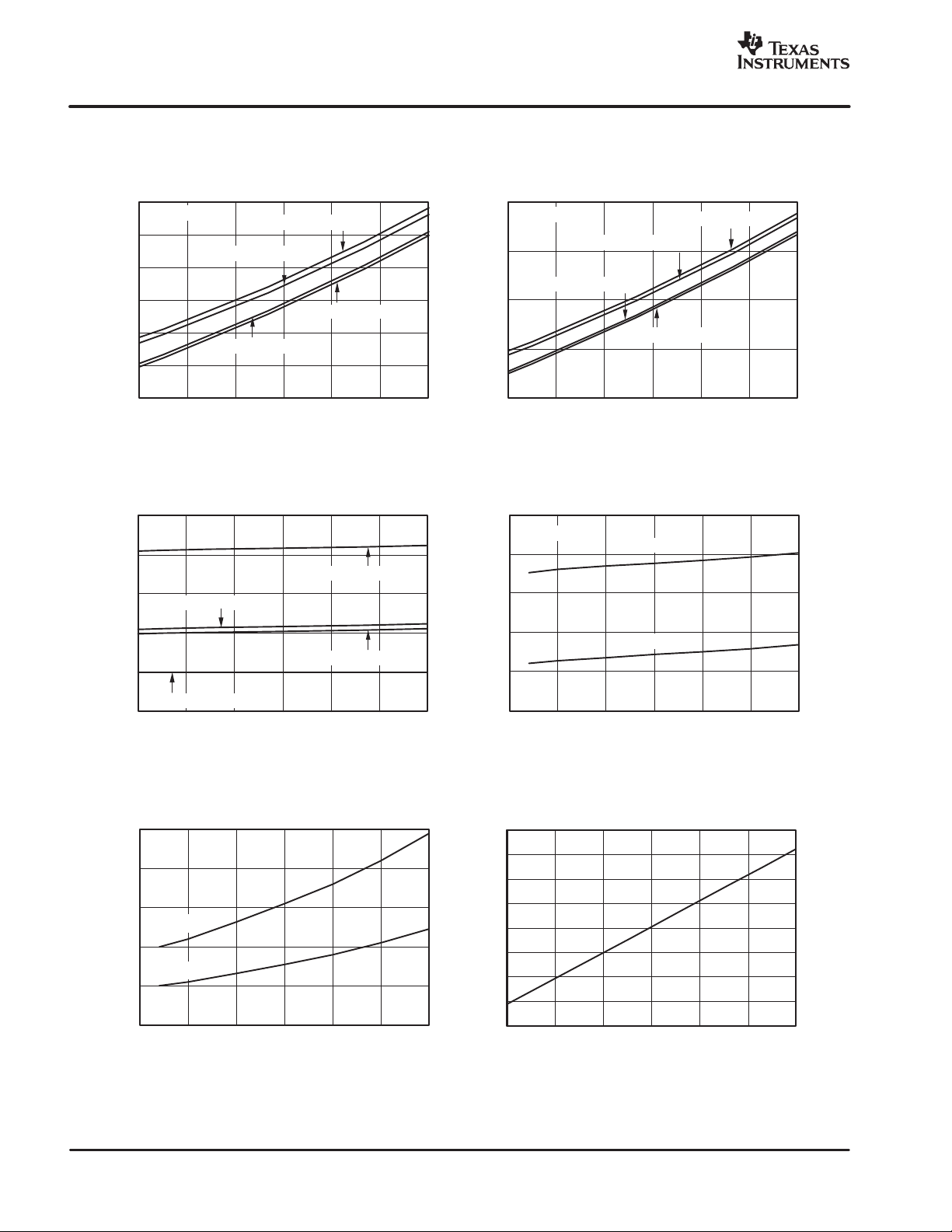
ANALOG CURRENT vs TEMPERATURE
ANALOG CURRENT vs TEMPERATURE
DIGITALCURRENT vs TEMPERATURE
ANALOG CURRENT vs SUPPLY VOLTAGE
DIGITALCURRENT vs SUPPLY VOLTAGE
TEMPERATURE SENSOR VOLTAGE vs TEMPERATURE
SBAS286A − JUNE 2003 − REVISED MARCH 2004
TYPICAL CHARACTERISTICS
At TA = −40°C to +85°C, AVDD = +5V, DVDD = +5V, f
= 2MHz, and V
CLK
= +2.5V , unless otherwise noted.
REF
www.ti.com
350
Buffer Off
325
f
300
A)
µ
275
Current (
250
225
200
−
55
CLK
f
−
25 35 65 95 125
f
=4MHz,AVDD=5V
CLK
=2MHz,AVDD=5V
=4MHz,AVDD=3V
CLK
5
Temperature (_C)
f
=2MHz,AVDD=3V
CLK
Figure 1
50
40
f
=4MHz,AVDD=5V
A)
30
µ
Current(
20
10
f
=2MHz,AVDD=5V
CLK
CLK
f
=4MHz,AVDD=3V
CLK
500
Buffer On
f
=2MHz,AVDD=5V
450
A)
µ
400
Current (
350
300
f
CLK
−
55
CLK
=4MHz,AVDD=3V
−
25 35 65 95 125
5
f
= 4MHz, AVDD = 5V
CLK
f
=2MHz,AVDD=3V
CLK
Temperature (_C)
Figure 2
450
f
=2MHz
CLK
400
A)
350
µ
300
Current (
250
Buffer On
Buffer Off
f
=2MHz,AVDD=3V
CLK
0
−
−
55
25 35 65 95 125
5
Temperature (_C)
Figure 3
50
40
A)
30
µ
Current(
f
=4MHz
CLK
20
f
=2MHz
CLK
10
0
3.53.0 4.0 4.5 5.0 5.52.5
Supply Voltage (V)
Figure 5
200
3.53.0 4.0 4.5 5.0 5.52.5
Supply Voltage (V)
Figure 4
150
140
130
120
110
100
90
80
Temperature Sensor Voltage (mV)
70
−
−
25 35 65 95 125
55
5
Temperature (_C)
Figure 6
6
Page 7
www.ti.com
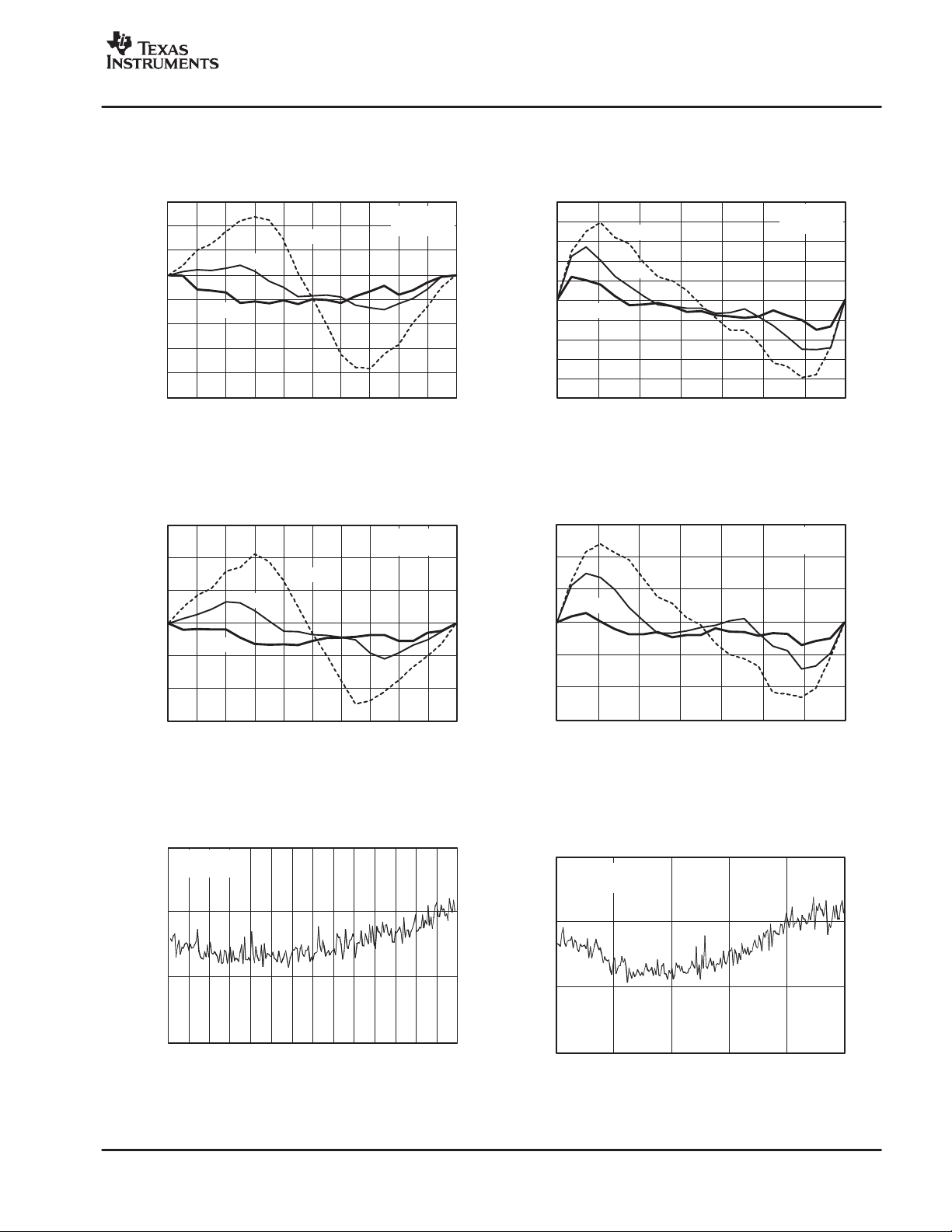
INTEGRAL NONLINEARITY vs INPUT VOLTAGE
INL (% of FSR)
INTEGRAL NONLINEARITY vs INPUT VOLTAGE
INL (% of FS R )
INTEGRAL NONLINEARITY vs INPUT VOLTAGE
INL (% o f FSR )
INTEGRAL NONLINEARITY vs INPUT VOLTAGE
INL (% o f F S R)
NOISE vs INPUT VOLTAGE
NOISE vs INPUT VOLTAGE
TYPICAL CHARACTERISTICS (CONTINUED)
At TA = −40°C to +85°C, AVDD = +5V, DVDD = +5V, f
= 2MHz, and V
CLK
SBAS286A − JUNE 2003 − REVISED MARCH 2004
= +2.5V , unless otherwise noted.
REF
0.0006
0.0004
0.0002
−
0.0002
−
0.0004
−
0.0006
−
0.0008
−
0.0010
0.0015
0.0010
0.0005
−
0.0005
f
=2MHz
CLK
−40_
C
+85_C
−
3
+25_C
−2−
1012345
Input Voltage, VIN(V)
0
−
−
4
5
Buffer Off
Figure 7
f
=4MHz
CLK
Buffer Off
−40_
C
+25_C
0
+85_C
0.0010
0.0008
0.0006
0.0004
0.0002
−
0.0002
−
0.0004
−
0.0006
−
0.0008
−
0.0010
0.0015
0.0010
0.0005
−
0.0005
−40_
C
+25_C
0
+85_C
−
−
−
3.5
2.5
−
1.5
0.5 0.5 1.5 2.5 3.5
Input Voltage, V
IN
Figure 8
−40_
C
+25_C
+85_C
0
(V)
f
CLK
Buffer On
f
CLK
Buffer On
=2MHz
=4MHz
−
−
0.0010
−
0.0015
−
5
−
−
4
3
−2−
10 1 2 3 4 5
Input Voltage, V
(V)
IN
Figure 9
1.5
f
=2MHz
CLK
Buffer On
1.0
0.5
Noise (ppm of FSR, rms)
0
3.5−3.0−2.5−2.0−1.5−1.0−0.5
−
0
0.5
Input Voltage, VIN(V)
1.0
1.5
2.0
2.5
3.0
3.5
Figure 11
0.0010
−
0.0015
Noise (ppm of FSR, rms)
1.5
1.0
0.5
−
3.5
0
−
f
=2MHz
CLK
Buffer Off
5
−
−
2.5
−
1.5
0.5 0.5 1.5 2.5 3.5
Input Voltage, V
(V)
IN
Figure 10
−
3
−
1135
Input Voltage, VIN(V)
Figure 12
7
Page 8

SBAS286A − JUNE 2003 − REVISED MARCH 2004
www.ti.com
OVERVIEW
The ADS1224 is an A/D converter comprised of a
delta-sigma modulator followed by a digital filter. A m u x
allows for one of four input channels to be selected. A
buffer can also be selected to increase the input
impedance. The modulator measures the differential
input signal VIN = (AINP – AINN) against the differential
reference V
= (VREFP – VREFN). Figure 13 shows
REF
a conceptual diagram of the device. The differential
reference is scaled internally so that the full-scale input
range i s ±2V
. The digital filter receives the modulator
REF
signal and provides a low-noise digital output. A 2-wire
serial interface indicates conversion completion and
provides the user with the output data.
ANALOG INPUTS (AINPx, AINNx)
The input signal to be measured is applied to the input
pins AINPx and AINNx. The positive internal input is
generalized as AINP, and the negative internal input is
generalized as AINN. The signal is selected though the
input mux, which is controlled by pins MUX0 and MUX1,
as shown in Table 1. The ADS1224 accepts differential
input signals, but can also measure unipolar signals.
When measuring unipolar (or single-ended signals)
with respect to ground, connect the negative input
(AINNx) to ground and connect the input signal to the
positive input (AINPx). Note that when the ADS1224 is
configured this way , only half of the converter full-scale
range is used since only positive digital output codes
are produced. An input buffer can be selected to
increase the input impedance of the A/D converter with
the BUFEN pin.
Table 1. Input Channel selection with MUX0 and
MUX1
DIGIT AL PINS SELECTED ANALOG INPUTS
MUX0 MUX1 POSITIVE INPUT NEGATIVE INPUT
0 0 AINP1 AINN1
0 1 AINP2 AINN2
1 0 AINP3 AINN3
1 1 AINP4 AINN4
AINP1
AINN1
AINP2
AINN2
AINP3
AINN3
AINP4
AINN4
TEMPEN
Temp
Sensor
AINP
Mux
AINN
MUX0
MUX1 BUFEN
Buffer
Σ
VREFPΣVREFN
+
V
IN
Modulator
2
∆Σ
Figure 13. Conceptual Diagram of the ADS1224
2V
−
V
REF
REF
Digital
Filter
and
Serial
Interface
CLK
SCLK
DRDY/DOUT
8
Page 9

www.ti.com
SBAS286A − JUNE 2003 − REVISED MARCH 2004
Analog Input Measurement without the Input Buffer
With the buffer disabled by setting the B UFEN pin l ow, the
ADS1224 measures the input signal using internal
capacitors that are continuously charged and discharged.
Figure 14 shows a sim plif ied schematic of the ADS1224
input circuitry, with F igure 15 showing t he on/off t imings of
the switches. The S
switches close during the input
1
sampling phase. With S1 closed, CA1 charges to AI NP,
CA2 charges to AINN, and CB charges to (AINP – AINN).
For the discharge phase, S1 opens first and then S
closes. CA1 and CA2 discharge to approximately A VDD/2
and CB discharges to 0V. This two-phase
sample/discharge cycle repeats with a frequency of
f
/32 (62.5kHz for f
CLK
ESD Protection
AVDD
AINPx
AINNx
AVDD
= 2MHz).
CLK
Mux
AINP
AINN
S
S
1
1
AVDD/2
S
S
AVDD/2
C
A1
3pF
2
C
B
6pF
2
C
A2
3pF
Figure 14. Simplified Input Structure with the
Buffer Turned Off
t
= 32/f
SAMPLE
ON
S
1
OFF
ON
S
2
OFF
CLK
AVDD/2
ZeffA=t
SAMPLE/CA1
AINPx
ZeffB=t
SAMPLE/CB
AINNx
ZeffA=t
SAMPLE/CA2
2
AVDD/2
NOTE: (1) f
CLK
=2MHz.
=6M
=3M
=6M
Ω
Ω
Ω
Figure 16. Effective Analog Input Impedances
with the Buffer Off
ESD diodes protect the inputs. To keep these diodes
from turning on, make sure the voltages on the input
pins do not go below GND by more than 100mV, and
likewise do not exceed AVDD by 100mV:
GND – 100mV < (AINP, AINN) < AVDD + 100mV
Analog Input Measurement with the Input Buffer
When the buffer is enabled by setting the BUFEN pin
high, a low-drift, chopper-stabilized input buffer is used
to achieve very high input impedance. The buffer
charges the input sampling capacitors, thus removing
the load from the measurement. Because the input
buffer is chopper-stabilized, the charging of parasitic
capacitances causes the charge to be carried away , as
if by resistance. The input impedance can be modeled
by a single resistor, as shown in Figure 17. The
impedance scales inversely with f
frequency, as in
CLK
the nonbuffered case.
AINP
(1)
Ω
1.2G
AINN
(1)
(1)
(1)
Figure 15. S1 and S2 Switch Timing for Figure 14
The constant charging of the input capacitors presents
a load on the inputs that can be represented by effective
impedances. Figure 16 shows the input circuitry with
the capacitors and switches of Figure 14 replaced by
their effective impedances. These impedances scale
inversely with f
frequency. For example, if f
CLK
CLK
frequency is reduced by a factor of 2, the impedances
will double.
NOTE: (1) f
CLK
=2MHz.
Figure 17. Effective Analog Input Impedances
with the Buffer On
Note that the analog inputs (listed in the Electrical
Characteristics table as Absolute Input Range) must
remain between GND + 0.05V to AVDD − 1.5V.
Exceeding this range degrades linearity and results in
performance outside the specified limits.
9
Page 10

SBAS286A − JUNE 2003 − REVISED MARCH 2004
www.ti.com
TEMPERATURE SENSOR
On-chip diodes provide temperature-sensing capability. By setting the TEMPEN pin high, the selected analog
inputs are disconnected and the inputs to the A/D
converter are connected to the anodes of two diodes
scaled to 1x and 64x in current and size inside the mux,
as shown in Figure 18. By measuring the difference in
voltage of these diodes, temperature changes can be
inferred from a baseline temperature. Typically, the
difference in diode voltages is 106mV at 25°C, with a
temperature coefficient of 360µV/°C. A similar structure
is used in the MSC1210 for temperature measurement.
For more information, see TI application report
SBAA100, Using the MSC121x as a High-Precision
Intelligent Temperature Sensor, available for download
at www.ti.com.
TEMPEN
AVDD
8I 1I
VOLTAGE REFERENCE INPUTS
(VREFP, VREFN)
The voltage reference used by the modulator is
generated from the voltage difference between VREFP
and VREFN: V
inputs use a structure similar to that of the analog
inputs. A simplified diagram of the circuitry on the
reference inputs is shown in Figure 19. The switches
and capacitors can be modeled with an effective
impedance of:
where f
Self Gain Cal
CLK
AVDD
= 2MHz.
= VREFP – VREFN. The reference
REF
t
sample
ǒ
Ǔ
ń16pF + 500kW
2
VREFP VREFN
AVDD
ESD
Protection
1X 8X
AINP1
AINN1
AINP2
AINN2
AINP3
AINN3
AINP4
AINN4
MUX0 MUX1
Figure 18. Measurement of the Temperature
Sensor in the Input Multiplexer
AINP
AINN
(1) f
CLK
AINP
=2MHz
AINN
16pF
Zeff= 500k
(1)
Ω
Figure 19. Simplified Reference input Circuitry
ESD diodes protect the reference inputs. To prevent
these diodes from turning on, make sure the voltages
on the reference pins do not go below GND by more
than 100mV, and likewise, do not exceed AVDD by
100mV:
GND – 100mV < (VREFP, VREFN) < AVDD + 100mV
During self gain calibration, all the switches in the input
multiplexer are opened, VREFN is internally connected to
AINN, and VREFP is connected to AINP. The input buffer
may be disabled or enabled during calibration. When the
buffer is dis abled, the reference pins will be driving the
circuitry shown in Figure 9 during self gain calibration,
resulting in increased loading. To prevent this additional
loading from introducing gain errors, make sure the
circuitry driving the reference pins has adequate drive
capability. When the buffer is enabled, the loading on the
reference p ins w ill b e m uch l ess, but the buffer w ill li mit the
10
Page 11
www.ti.com
SBAS286A − JUNE 2003 − REVISED MARCH 2004
allowable voltage range on VREFP and VREFN during
self or self gain calibrat ion as the ref erence pins must
remain within the specified input range of the buffer in
order to establish proper gain calibration.
For best performance, V
be raised as high as AVDD. When V
should b e A VDD/2, but it can
REF
REF
exceeds
AVDD/2, it is not possible to reach the full-scale digital
output value corresponding to ±2V
, since this r equires
REF
the analog inputs to exceed the power supplies. For
example, if V
= AVDD = 5V, the positive full-scale
REF
signal is 10V. The maximum positive input signal that can
be supplied before the ESD diodes turn on is when AINP
= 5.1V and AINN = –0.1V, resulting in VIN = 5.2V.
Therefore, it is not possible to reach the positive (or
negative) full-scale readings in this configuration. The
digital output codes are limited to approximately one half
of the entire range. For best performance, bypass the
voltage reference inputs with a 0.1µF capac itor between
VREFP and VREFN. Place the capacitor as close as
possible to the pins.
CLOCK INPUT (CLK)
This digital input supplies the system clock to the
ADS1224. The CLK frequency can be increased to
speed up the data rate. CLK must be left running during
normal operation. It may be turned off during Standby
mode to save power, but this is not required. The CLK
input may be driven with 5V logic, regardless of the
DVDD or AVDD voltage.
Minimize the overshoot and undershoot on CLK for the
best analog performance. A small resistor in series with
CLK (10Ω to 100Ω) can often help. CLK can be
generated from a number of sources including
standalone crystal oscillators and microcontrollers.
the pin can be forced high with an additional SCLK. It will
then stay high until new data is ready. This is useful
when polling on the status of DRDY/DOUT to determine
when to begin data retrieval.
SERIAL CLOCK INPUT (SCLK)
This digital input shifts serial data out with each rising
edge. As with CLK, this input may be driven with 5V
logic regardless of the DVDD or AVDD voltage. There
is hysteresis built into this input, but care should still be
taken to ensure a clean signal. Glitches or slow-rising
signals can cause unwanted additional shifting. For this
reason, it is best to make sure the rise-and-fall times of
SCLK are less than 50ns.
FREQUENCY RESPONSE
The ADS1224 frequency response for f
shown in Figure 20. The frequency response repeats at
multiples of the modulator sampling frequency of
62.5kHz. The overall response is that of a low-pass filter
with a −3db cutoff frequency of 31.5Hz. As shown, the
ADS1224 does a good job attenuating out to 60kHz. For
the best resolution, limit the input bandwidth to less than
this value to keep higher frequency noise from affecting
performance. Often, a simple RC filter on the ADS1224
analog inputs is all that is needed.
0
−
20
−
40
= 2MHz is
CLK
DATA READY/DATA OUTPUT (DRDY/DOUT)
This digital output pin serves two purposes. First, it
indicates when new data is ready by going LOW.
Afterwards, on the first rising edge of SCLK, the
DRDY/DOUT pin changes function and begins
outputting the conversion data, most significant bit
(MSB) first. Data is shifted out on each subsequent
SCLK rising edge. After all 24 bits have been retrieved,
Gain (dB)
−
60
−
80
−
100
31250 625000
Input Frequency (Hz)
Figure 20. Frequency Response
11
Page 12

SBAS286A − JUNE 2003 − REVISED MARCH 2004
www.ti.com
To help see the response at lower frequencies,
Figure 21 illustrates the response out to 1kHz. Notice
that signals at multiples of 120Hz are rejected. The
ADS1224 data rate and frequency response scale
directly with CLK frequency. For example, if f
CLK
increases from 2MHz to 4MHz, the data rate increases
from 120SPS to 240SPS, while the notches increase
from 120Hz to 240Hz.
0
−
20
−
40
Gain (dB)
−
60
−
80
−
100
500 600 700 800 900100 200 300 400 1k0
Input Frequency (Hz)
Figure 21. Frequency Response to 1kHz
Rejecting 50Hz or 60Hz noise is as simple as choosing
the clock frequency. If simultaneous rejection of 50Hz
and 60Hz noise is desired, f
= 910kHz can be
CLK
chosen. The data rate becomes 54.7sps and the
frequency response of the ADS1224 rejects the 50Hz
and 60Hz noise to below 60dB. The frequency
response of the ADS1224 near 50Hz and 60Hz with
f
= 910kHz is shown in Figure 22.
CLK
0
−
20
−
40
Gain (dB)
−
60
−
80
−
100
Input Frequency (Hz)
8030 40 50 60 70
Figure 22. Frequency Response Near 50Hz and
60Hz with f
CLK
= 910kHz
SETTLING TIME
After changing the input multiplexer, selecting the input
buffer, or using temperature sensor, the first data is fully
settled. In the ADS1224, the digital filter is allowed to
settle after toggling any of the MUX0, MUX1, BUFEN,
or TEMPEN pins. Toggling of any of these digital pins
will cause the input to switch to the proper channel, start
conversions, and hold the DRDY/DOUT line high until
the digital filter is fully settled. For example, if MUX0
changes from low to high, selecting a different input
channel, DRDY/DOUT immediately goes high and the
conversion process restarts. DRDY/DOUT goes low
when fully settled data is ready for retrieval. There is no
need to discard any data. Figure 23 shows the timing of
the DRDY/DOUT line as the input multiplexer changes.
12
MUX0
V
DRDY/DOUT
SYMBOL DESCRIPTION MIN MAX UNITS
(1)
Abrupt change in internal VINdue to status change (for example, switch channels, temp sensor, buffer enable)
IN
t
1
ADS1224 holds DRDY/DOUT
until digital filter settles
DRDY/DOUT suppressed after status change
(1)
t
1
Values given for f
Settling time (DRDY/DOUT held high) after a change in any of the 25.9 26.4 ms
MUX0, MUX1, BUFEN, or TEMPEN pins
= 2MHz. For different f
CLK
frequencies, scale proportional to CLK period.
CLK
Figure 23. Example of Settling Time After Changing the Input Multiplexer
Fully settled
data ready
Page 13

www.ti.com
SBAS286A − JUNE 2003 − REVISED MARCH 2004
The ADS1224 uses a Sinc3 digital filter to improve noise
performance. Therefore, in certain instances, large
changes in input will require settling time. For example,
an external multiplexer in front of the ADS1224 can put
large changes in input voltage by simply switching input
channels. Abrupt changes in the input will require three
data cycles to settle. When continuously converting,
four readings may be necessary to settle the data. If the
change in input occurs in the middle of the first conversion, three more full conversions of the fully settled input
will be required to get fully settled data. Discard the first
three readings because they will contain only partially−
settled data. Figure 24 illustrates the settling time for
the ADS1224 in Continuous Conversion mode.
If the input is known to change abruptly, the mux can be
quickly switched to an alternate channel and quickly
switched back to the original channel. By toggling the
mux, the ADS1224 resets the digital filter and initiates a
new conversion. During this time, the DRDY
/DOUT line
is held high until fully-settled data is available.
DATA FORMAT
The ADS1224 outputs 24 bits of data in binary two’s
complement format. The least significant bit (LSB) has
a weight of (2VREF)/(223 – 1). The positive full-scale
input produces an output code of 7FFFFFh and the
negative full-scale input produces an output code of
800000h. The output clips at these codes for signals
exceeding full-scale. Table 2 summarizes the ideal
output codes for different input signals.
Table 2. Ideal Output Code vs Input Signal
INPUT SIGNAL V
(AINP − AINN)
w +2V
+2V
223* 1
−2V
223* 1
v −2V
REF
(1)
Excludes effects of noise, INL, offset, and gain errors.
IN
REF
REF
0 000000h
REF
23
2
ǒ
223* 1
Ǔ
IDEAL OUTPUT CODE
7FFFFFh
000001h
FFFFFFh
800000h
(1)
DATA RETRIEVAL
The ADS1224 continuously converts the analog input
signal. To retrieve data, wait until DRDY/DOUT goes
low, as shown in Figure 25. After this occurs, begin
shifting out the data by applying SCLKs. Data is shifted
out MSB first. It is not required to shift out all 24 bits of
data, but the data must be retrieved before the new data
is updated (see t2) or else it will be overwritten. Avoid
data retrieval during the update period. DRDY/DOUT
remain at the state of the last bit shifted out until it is
taken high (see t6), indicating that new data is being
updated. To avoid having DRDY/DOUT remain in the
state of the last bit, shift a 25th SCLK to force
DRDY/DOUT high (see Figure 26). This technique is
useful when a host controlling the ADS1224 is polling
DRDY/DOUT to determine when data is ready.
V
DRDY/DOUT
Abrupt change in external V
IN
Starto f
conversion
Conversion
time
First Conversion;
includes
unsettled V
IN
Second Conversion;
settled, but
V
IN
digital filter
IN
unsettled
Third Conversion;
settled, but
V
IN
digital filter
unsettled
Fourth Conversion;
anddigital filter
V
IN
bothsettled
Figure 24. Settling Time in Continuous Conversion Mode
13
Page 14

SBAS286A − JUNE 2003 − REVISED MARCH 2004
Data Ready
DRDY/DOUT 23 22 21
www.ti.com
Data
NewData Ready
LSBMSB
0
SCLK
t
4
t
2
124
t
3
t
3
t
7
t
5
SYMBOL DESCRIPTION MIN MAX UNITS
t
DRDY/DOUT low to first SCLK rising edge 0 ns
2
t
SCLK positive or negative pulse width 100 ns
3
(1)
t
4
t
6
t
7
(1)
Values given for f
SCLK rising edge to new data bit valid: propogation delay 50 ns
t
SCLK rising edge to old data bit valid: hold time 0 ns
5
(1)
Data updating; no readback allowed 48 µs
(1)
Conversion time (1/data rate) 8.32 8.32 ms
= 2MHz. For different f
CLK
frequencies, scale proportional to CLK period.
CLK
Figure 25. Data Retrieval Timing
Data
Data Ready
t
6
New Data Ready
14
DRDY/DOUT
SCLK
23
22 21 0
12425
25th SCLK to Force DRDY/DOUT High
Figure 26. Data Retrieval with DRDY/DOUT Forced High Afterwards
Page 15

www.ti.com
SBAS286A − JUNE 2003 − REVISED MARCH 2004
SELF-CALIBRATION
Self-calibration can be initiated at any time, although in
many applications the ADS1224 drift performance is so
good that the self-calibration performed automatically
at power-up is all that is needed. To initiate
self-calibration, apply at least two additional SCLKs
after retrieving 24 bits of data. Figure 27 shows the
timing pattern. The 25th SCLK will send DRDY/DOUT
high. The falling edge of the 26th SCLK will begin the
calibration cycle. Additional SCLK pulses may be sent
after the 26th SCLK; however, activity on SCLK should
be minimized during calibration for best results.
When the calibration is complete, DRDY/DOUT goes
low, indicating that new data is ready. There is no need
to alter the analog input signal applied to the ADS1224
during calibration; the input pins are disconnected
within the A/D converter and the appropriate signals are
applied internally and automatically. The first
conversion after a calibration is fully settled and valid for
use. The time required for a calibration depends on two
independent signals: the falling edge of SCLK and an
internal clock derived from CLK. Variations in the
internal calibration values will change the time required
for calibration (t8) within the range given by the min/max
specs. t11 and t12 described in the next section are
affected likewise.
STANDBY MODE
Standby mode dramatically reduces power
consumption (typically < 1µW with CLK stopped) by
shutting down all of the active circuitry. To enter Standby
mode, simply hold SCLK high after DRDY/DOUT goes
low, as shown in Figure 28. Standby mode can be
initiated at any time during readback; it is not necessary
to retrieve all 24 bits of data beforehand.
When t11 has p assed with S CLK held h igh, Standby mode
will activate. DRDY/DOUT stays high when Standby
mode begins. SCLK must remain high to stay in Standby
mode. To exit St andby mode (wakeup), set SCLK low.
The first data after exiting Standby mode is valid. It is not
necessary to stop CLK during Standby mode, but doing
so will furt her reduc e the digital supply curr ent.
Standby Mode With Self-Calibration
Self-calibration can be set to run immediately after
exiting Standby mode. This is useful when the
ADS1224 is put in Standby mode for long periods of
time and self-calibration is desired afterwards to
compensate for temperature or supply voltage
changes.
To force a self-calibration with Standby mode, shift 25
bits out before taking SCLK high to enter Standby
mode. Self-calibration then begins after wakeup.
Figure 29 shows the appropriate timing. Note the extra
time needed after wakeup for calibration before data is
ready. The first data after Standby mode with
self-calibration is fully settled and can be used.
23DRDY/DOUT
SCLK 1 24
SYMBOL DESCRIPTION MIN MAX UNITS
(1)
t
8
(1)
Values given for f
First data ready after calibration 77.1 77.9 ms
= 2MHz. For different f
CLK
Figure 27. Self-Calibration Timing
Data Ready After Calibration
Calibration Begins
25 26
t
8
frequencies, scale proportional to CLK period.
CLK
2322 21 0
15
Page 16

SBAS286A − JUNE 2003 − REVISED MARCH 2004
www.ti.com
DRDY/DOUT 23 22 21
SCLK
SYMBOL DESCRIPTION MIN MAX UNITS
(2)
124
t
9
(1)
t
9
t
10
t
11
Values given for f
SCLK high after DRDY/DOUT goes low to activate Standby mode 0 8.272 ms
(1)
Standby mode activation time 8.272 8.304 ms
(1)
Data ready after exiting Standby mode 27.7 28.1 ms
= 2MHz. For different f
CLK
Figure 28. Standby Mode Timing (can be used for single conversions)
DRDY/DOUT 23
22 21 0 23
Standby Mode
023
t
10
frequencies, scale proportional to CLK period.
CLK
Standby Mode
Start Conversion
Begin Calibration
Data Ready
t
11
Data Ready After Calibration
SCLK
(1)
12425
t
10
SYMBOL DESCRIPTION MIN MAX UNITS
(1)
t
12
Values given for f
Data ready after exiting Standby mode and calibration 78.8 79.7 ms
= 2MHz. For different f
CLK
Figure 29. Standby Mode with Self-Calibration Timing (can be used for single conversions)
SINGLE CONVERSIONS
When only single conversions are needed, Standby
mode can be used to start and stop the ADS1224. To
make a single conversion, first enter the Standby mode
holding SCLK high. Now, when ready to start the
conversion, take SCLK low. The ADS1224 wakes up
and begins the conversion. Wait for DRDY/DOUT to go
low, and then retrieve the data. Afterwards, take SCLK
t
12
frequencies, scale proportional to CLK period.
CLK
high to stop the ADS1224 from converting and re-enter
Standby mode. Continue to hold SCLK high until ready
to start the next conversion. Operating in this fashion
greatly reduces power consumption since the
ADS1224 is shut down while idle between conversions.
Self-calibrations can be performed prior to the start of
the single conversions by using the waveform shown in
Figure 29.
16
Page 17

www.ti.com
SBAS286A − JUNE 2003 − REVISED MARCH 2004
APPLICATIONS INFORMATION
GENERAL RECOMMENDATIONS
The ADS1224 is a high-resolution A/D converter.
Achieving optimal device performance requires careful
attention to the support circuitry and printed circuit
board (PCB) design. Figure 30 shows the basic
connections for the ADS1224. As with any precision
circuit, be sure to use good supply bypassing capacitor
techniques. A smaller value ceramic capacitor in
parallel with a larger value tantulum capacitor works
well. Place the capacitors, in particular the ceramic
ones, close to the supply pins. Use a ground plane and
tie the ADS1224 GND pin and bypass capacitors
directly to it. Avoid ringing on the digital inputs. Small
resistors (≈100Ω) in series with the digital pins can help
by controlling the trace impedance. Place these
resistors at the source end.
+5V
VIN
VIN
Ω
301
P
301
N
0.1µF10µF
1
Ω
100
Ω
100
Ω
100
Ω
100
220pF
0.1µF
Ω
220pF
100
100
100
2
Ω
3
4
Ω
5
6
Ω
7
8
9
10
ADS1224
DVDD
SCLK
CLK
DRDY/DOUT
MUX0
MUX1
TEMPEN
BUFEN
AINP4
AINN4
Pay special attention to the reference and analog
inputs. These are the most critical circuits. Bypass the
voltage reference using similar techniques to the supply
voltages. The quality of the reference directly affects
the overall accuracy of the device. Make sure to use a
low noise and low drift reference such as the REF1004.
Often, only a simple RC filter is needed on the inputs.
This circuits limits the higher frequency noise. Avoid
low-grade dielectrics for the capacitors and place them
as close as possible to the input pins. Keep the traces
to the input pins short, and carefully watch how they are
routed on the PCB.
After the power supplies and reference voltage have
stabilized, issue a self-calibration command to
minimize offset and gain errors.
+5V
+2.5V Reference
AVDD
VREFP
VREFN
GND
AINN1
AINP1
AINN2
AINP2
AINN3
AINP3
0.1µF 10µF
20
19
18
17
16
15
14
13
12
11
0.1µF 10µF
Same as shown for AINP4 and AINN4.
Figure 30. Basic Connections
17
Page 18

SBAS286A − JUNE 2003 − REVISED MARCH 2004
www.ti.com
MULTICHANNEL SYSTEMS
Multiple ADS1224s can be operated in parallel to
measure multiple input signals. Figure 31 shows an
example of an eight-channel system. For simplicity, the
supplies and reference circuitry are not shown. The
same CLK signal should be applied to all devices. To
synchronize the ADS1224s, connect the same SCLK
signal to all devices. Then place all the devices in
Standby mode. Afterwards, starting a conversion will
synchronize all the ADS1224s; that is, they will sample
the input signals simultaneously. The DRDY/DOUT
outputs will go low at approximately the same time after
synchronization. When reading data from the devices,
the data appears in parallel on DRDY/DOUT as a result
of the common SCLK connection.
ADS1224
AINP1
CLK
SCLK
DRDY/DOUT
OUT1
Inputs
MUX Select
AINN1
…
AINP4
AINN4
MUX0
MUX1
The falling edges of DRDY
/DOUT, indicating that new
data is ready, will vary with respect to each other no
more than time t
. This variation is due to possible
13
differences in the ADS1224 internal calibration settings.
To account for this, when using multiple devices, either
wait for t13 to pass after seeing one DRDY/DOUT go
low, or wait until all DRDY/DOUTs have gone low before
retrieving data.
Note that changing channels (using the MUX0 and
MUX1 pins), or using the input buffer (BUFEN) or the
temperature sensor (TEMPEN), may require more care
to settle the digital filter. For example, if the MUX0 pin
is toggled on one device and not the other, the
DRDY/DOUT line will be held high until the conversion
settles on the first device. The latter device will continue
conversions through this time. See the Settling Time
section of this datasheet for further details.
ADS1224
AINP1
AINN1
Inputs
MUX Select
SYMBOL DESCRIPTION MIN MAX UNITS
(1)
t
13
(1)
Values given for f
…
AINP4
AINN4
MUX0
MUX1
Difference between DRDY/DOUTs going low in multichannel ±0.8 ms
systems
CLK
CLK
SCLK
DRDY/DOUT
CLK and SCLK
Sources
= 2MHz. For different f
OUT2
frequencies, scale proportional to CLK period.
CLK
OUT1
OUT2
t
13
Figure 31. Example of Using Multiple ADS1224s in Parallel
18
Page 19

www.ti.com
SBAS286A − JUNE 2003 − REVISED MARCH 2004
VESSEL WEIGHING WITH FOUR LOAD
CELLS
In vessel weighing systems, four load cells are
frequently employed to measure the weight of the
vessel and its contents. The output of the load cells are
usually combined in an external summing junction box
that balances the load cells’ sensitivities for accuracy.
The four differential inputs of the ADS1224 allow for
direct measurement of the four load cells individually. In
this way , the mechanical adjustments performed inside
the summing junction box are eliminated and are
replaced by digital summing of the load cells in
software. Figure 32 shows an example of such a
system.
The reference voltage of the ADS1224 is derived by
dividing down the AVDD supply voltage to 2.5V, while
the load cell has a positive full-scale output of 10mV . In
the figure, a low drift, dual op amp (OP A2335) provides
a differential in/differential out amplifier with a gain of
499V/V (G = 1 + 2RF/RG). Gain on the load cell gives
the amplifier a full-scale output of 5V.
Each load cell input uses an external amplifier. The
outputs of the amplifiers connect to the analog inputs of
the ADS1224 through a low-pass filter. The cut-off
frequency is set to 360Hz, allowing full settling in a
single measurement cycle. A lower cut-off frequency
can be used to reduce noise from mechanical
vibrations, but at the expense of filter settling time.
The internal buffer of the ADS1224 is disabled, allowing
the VREFN pin to be grounded. Note that the loading
from the reference inputs will change the effective
reference voltage. The effective input impedance into
the VREFP and VREFN pins will lower the reference
voltage seen at these pins. At 2MHz, input impedance
is approximately 500kΩ. For the reference circuit shown
in Figure 32, this lowers the effective reference voltage
by approximately 0.1%.
5V
+3V
Ω
350
Load Cell
NOTE: (1) Low−drift resistors.
Shield ed
Replicate for Chann e ls 2, 3 and 4
Cable
RFI
Filt er
RFI
Filt er
G=1+
RFI
Filt er
RFI
Filt er
100
2R
R
10
R
G
100
(1)
Ω
1k
VREFP
(1)
Ω
1k
VREFN
Ω
Ω
AINP1
0.22µF
AINN1
AINP2
AINN2
AINP3
AINN3
AINP4
AINN4
1/2
OPA2335
(1)
F
Ω
(1)
F
Ω
1/2
OPA2335
0.1µF
1k
1k
5V
Ω
R
F
2.49k
G
(1)
R
Ω
2.49k
Ω
0.1µF 0.1µF 0.1µF1µF
AVDD
DVDD
BUFEN
TEMPEN
ADS1224
CLK
SCLK
DRDY/DOUT
MUX0
MUX1
GND
Figure 32. Vessel Weighing System with Four Load Cells
DVCC
MSP 430 F 4 1x
P1.1/TA0/MCLK
P1.2/TA1
P1.0/TA0
P1.6/CA0
P1.7/CA1
XOUT/TCLK
GND
AVCC
XIN
19
Page 20

SBAS286A − JUNE 2003 − REVISED MARCH 2004
SUMMARY OF SERIAL INTERFACE WAVEFORMS
www.ti.com
DRDY/DOUT
SCLK
DRDY/DOUT
SCLK
DRDY/DOUT
SCLK
23 22 21 0
MSB LSB
124
(a) Data Retrieval
23 22 21 0
12425
(b) Data Retrieval with DRDY/DOUT Forced High Afterwards
Data Ready
After Calibration
23 22 21 0
1242526
Begin Calibration
DRDY/DOUT
SCLK
DRDY/DOUT
SCLK
(c) Self−Calibration
Standby Mode
23 22 21 0
124
(d) Standby Mode/Single Conversions
Standby Mode
23 22 21 0
12425
(e) Standby Mode/Single Conversions with Self−Calibration
Figure 33. Summary of Serial Interface Waveforms
Data Ready
Start
Conversion
Data Ready
AfterCalibration
Begin Calibration
20
Page 21

PACKAGE OPTION ADDENDUM
www.ti.com
29-Mar-2004
PACKAGING INFORMATION
ORDERABLE DEVICE STATUS(1) PACKAGE TYPE PACKAGE DRAWING PINS PACKAGE QTY
ADS1224IPWR ACTIVE TSSOP PW 20 2500
ADS1224IPWT ACTIVE TSSOP PW 20 250
(1) The marketing status values are defined as follows:
ACTIVE: Product device recommended for new designs.
LIFEBUY: TI has announced that the device will be discontinued, and a lifetime-buy period is in effect.
NRND: Not recommended for new designs. Device is in production to support existing customers, but TI does not recommend using this part in
a new design.
PREVIEW: Device has been announced but is not in production. Samples may or may not be available.
OBSOLETE: TI has discontinued the production of the device.
Page 22

MECHANICAL DATA
MTSS001C – JANUARY 1995 – REVISED FEBRUARY 1999
PW (R-PDSO-G**) PLASTIC SMALL-OUTLINE PACKAGE
14 PINS SHOWN
0,65
1,20 MAX
14
0,30
0,19
8
4,50
4,30
PINS **
7
Seating Plane
0,15
0,05
8
1
A
DIM
14
0,10
6,60
6,20
M
0,10
0,15 NOM
0°–8°
2016
Gage Plane
24
0,25
0,75
0,50
28
A MAX
A MIN
NOTES: A. All linear dimensions are in millimeters.
B. This drawing is subject to change without notice.
C. Body dimensions do not include mold flash or protrusion not to exceed 0,15.
D. Falls within JEDEC MO-153
3,10
2,90
5,10
4,90
5,10
4,90
6,60
6,40
7,90
7,70
9,80
9,60
4040064/F 01/97
POST OFFICE BOX 655303 • DALLAS, TEXAS 75265
Page 23

IMPORTANT NOTICE
Texas Instruments Incorporated and its subsidiaries (TI) reserve the right to make corrections, modifications,
enhancements, improvements, and other changes to its products and services at any time and to discontinue
any product or service without notice. Customers should obtain the latest relevant information before placing
orders and should verify that such information is current and complete. All products are sold subject to TI’s terms
and conditions of sale supplied at the time of order acknowledgment.
TI warrants performance of its hardware products to the specifications applicable at the time of sale in
accordance with TI’s standard warranty. Testing and other quality control techniques are used to the extent TI
deems necessary to support this warranty . Except where mandated by government requirements, testing of all
parameters of each product is not necessarily performed.
TI assumes no liability for applications assistance or customer product design. Customers are responsible for
their products and applications using TI components. To minimize the risks associated with customer products
and applications, customers should provide adequate design and operating safeguards.
TI does not warrant or represent that any license, either express or implied, is granted under any TI patent right,
copyright, mask work right, or other TI intellectual property right relating to any combination, machine, or process
in which TI products or services are used. Information published by TI regarding third-party products or services
does not constitute a license from TI to use such products or services or a warranty or endorsement thereof.
Use of such information may require a license from a third party under the patents or other intellectual property
of the third party, or a license from TI under the patents or other intellectual property of TI.
Reproduction of information in TI data books or data sheets is permissible only if reproduction is without
alteration and is accompanied by all associated warranties, conditions, limitations, and notices. Reproduction
of this information with alteration is an unfair and deceptive business practice. TI is not responsible or liable for
such altered documentation.
Resale of TI products or services with statements different from or beyond the parameters stated by TI for that
product or service voids all express and any implied warranties for the associated TI product or service and
is an unfair and deceptive business practice. TI is not responsible or liable for any such statements.
Following are URLs where you can obtain information on other Texas Instruments products and application
solutions:
Products Applications
Amplifiers amplifier.ti.com Audio www.ti.com/audio
Data Converters dataconverter.ti.com Automotive www.ti.com/automotive
DSP dsp.ti.com Broadband www.ti.com/broadband
Interface interface.ti.com Digital Control www.ti.com/digitalcontrol
Logic logic.ti.com Military www.ti.com/military
Power Mgmt power.ti.com Optical Networking www.ti.com/opticalnetwork
Microcontrollers microcontroller.ti.com Security www.ti.com/security
Telephony www.ti.com/telephony
Video & Imaging www.ti.com/video
Wireless www.ti.com/wireless
Mailing Address: Texas Instruments
Post Office Box 655303 Dallas, Texas 75265
Copyright 2004, Texas Instruments Incorporated
 Loading...