

Page 1
查询ADS1217供应商查询ADS1217供应商
A
D
S
1
2
1
7
SBAS260B – MAY 2002 – REVISED OCTOBER 2004
8-Channel, 24-Bit
ANALOG-TO-DIGITAL CONVERTER
ADS1217
FEATURES
● 24 BITS NO MISSING CODES
● INL: 0.0012% of FSR (max)
● FULL-SCALE INPUT: ±2V
REF
● PGA FROM 1 TO 128
● 22 BITS EFFECTIVE RESOLUTION
(PGA = 1), 19 BITS (PGA = 128)
● SINGLE CYCLE SETTLING MODE
● PROGRAMMABLE DATA OUTPUT RATES
UP TO 1kHz
● ON-CHIP 1.25V/2.5V REFERENCE
● ON-CHIP CALIBRATION
● SPI COMPATIBLE
● POWER SUPPLY: 2.7V to 5.25V
● < 1mW POWER CONSUMPTION, VDD = 3V
APPLICATIONS
● INDUSTRIAL PROCESS CONTROL
● LIQUID/GAS CHROMATOGRAPHY
● BLOOD ANALYSIS
● SMART TRANSMITTERS
● PORTABLE INSTRUMENTATION
● WEIGH SCALES
● PRESSURE TRANSDUCERS
IDAC2
IDAC1
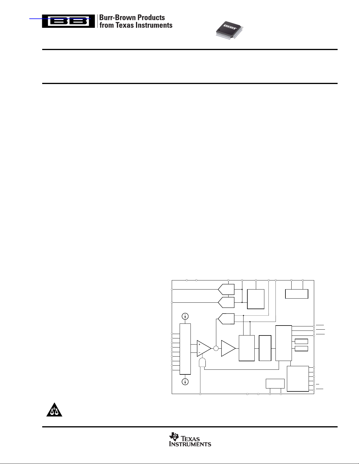
DESCRIPTION
The ADS1217 is a precision, wide dynamic range, deltasigma, Analog-to-Digital (A/D) converter with 24-bit resolution operating from 2.7V to 5.25V supplies. The delta-sigma,
A/D converter provides up to 24 bits of no missing code
performance and effective resolution of 22 bits.
The eight input channels are multiplexed. Internal buffering
can be selected to provide a very high input impedance for
direct connection to transducers or low-level voltage signals.
Burnout current sources are provided that allow for the
detection of an open or shorted sensor. An 8-bit Digital-toAnalog Converter (DAC) provides an offset correction with a
range of 50% of the FSR (Full-Scale Range).
The PGA (Programmable Gain Amplifier) provides selectable
gains of 1 to 128 with an effective resolution of 19 bits at a gain
of 128. The A/D conversion is accomplished with a 2nd-order,
delta-sigma modulator and programmable sinc filter. The
reference input is differential and can be used for ratiometric
measurements. The onboard current DACs operate independently with the maximum current set by an external resistor.
The serial interface is SPI compatible. Eight bits of digital I/O
are also provided that can be used for input or output. The
ADS1217 is designed for high-resolution measurement applications in smart transmitters, industrial process control, weigh
scales, chromatography, and portable instrumentation.
V
AGND AV
R
REFOUTVRCAPVREF+VREF–
8-Bit
IDAC
8-Bit
IDAC
DAC
Voltage
Reference
DD
X
X
IN
Clock Generator
OUT
Please be aware that an important notice concerning availability, standard warranty, and use in critical applications of
Texas Instruments semiconductor products and disclaimers thereto appears at the end of this data sheet.
All trademarks are the property of their respective owners.
PRODUCTION DATA information is current as of publication date.
Products conform to specifications per the terms of Texas Instruments
standard warranty. Production processing does not necessarily include
testing of all parameters.
A
IN
A
IN
A
IN
A
IN
A
IN
A
IN
A
IN
A
IN
A
INCOM
0
1
2
3
4
5
6
7
www.ti.com
MUX
Offset
DAC
+
BUF PGA
PDWN
DYSNC
2nd-Order
Modulator
DD
Program-
mable
Digital
Filter
Digital I/O
Interface
Controller
D7BUFEN ...D0DGNDDV
Registers
Serial Interface
RAM
RESET
POL
SCLK
D
IN
D
OUT
CS
DRDY
Copyright © 2002-2004, Texas Instruments Incorporated
Page 2

ABSOLUTE MAXIMUM RATINGS
(1)
AVDD to AGND ...................................................................... –0.3V to +6V
DV
to DGND...................................................................... –0.3V to +6V
DD
Input Current ............................................................... 100mA, Momentary
Input Current ................................................................. 10mA, Continuous
A
................................................................... GND –0.5V to AVDD + 0.5V
IN
AV
to DVDD........................................................................... –6V to +6V
DD
AGND to DGND ................................................................. –0.3V to +0.3V
Digital Input Voltage to GND.................................... –0.3V to DV
Digital Output Voltage to GND ................................. –0.3V to DV
Maximum Junction Temperature ................................................... +150°C
+ 0.3V
DD
+ 0.3V
DD
Operating Temperature Range ......................................... –40°C to +85°C
Storage Temperature Range .......................................... –60°C to +150°C
Lead Temperature (soldering, 10s) .............................................. +300°C
NOTE: (1) Stresses above those listed under “Absolute Maximum Ratings” may
cause permanent damage to the device. Exposure to absolute maximum
conditions for extended periods may affect device reliability.
ELECTROSTATIC
DISCHARGE SENSITIVITY
This integrated circuit can be damaged by ESD. Texas Instruments recommends that all integrated circuits be handled with
appropriate precautions. Failure to observe proper handling
and installation procedures can cause damage.
ESD damage can range from subtle performance degradation
to complete device failure. Precision integrated circuits may be
more susceptible to damage because very small parametric
changes could cause the device not to meet its published
specifications.
PACKAGE/ORDERING INFORMATION
(1)
SPECIFIED
PACKAGE TEMPERATURE PACKAGE ORDERING TRANSPORT
PRODUCT PACKAGE-LEAD DESIGNATOR RANGE MARKING NUMBER MEDIA, QUANTITY
ADS1217 TQFP-48 PFB –40°C to +85°C ADS1217 ADS1217IPFBT Tape and Reel, 250
" """"ADS1217IPFBR Tape and Reel, 2000
NOTE: (1) For the most current package and ordering information, see the Package Option Addendum located at the end of this data sheet.
ELECTRICAL CHARACTERISTICS: AVDD = 5V
All specifications at –40°C to +85°C, AVDD = +5V, DVDD = +2.7V to 5.25V, f
unless otherwise specified.
PARAMETER CONDITIONS MIN TYP MAX UNITS
ANALOG INPUT
(AIN0 – AIN7, A
Full-Scale Input Voltage (A
Analog Input Voltage Buffer OFF AGND – 0.1 AV
INCOM
)
) – (A
IN+
IN–
Buffer ON AGND + 0.05 AV
Differential Input Impedance Buffer OFF 10/PGA MΩ
Input Current Buffer ON 0.5 nA
Bandwidth
Fast Settling Filter –3dB 0.469f
2
Sinc
Filter –3dB 0.318f
3
Sinc
Filter –3dB 0.262f
Programmable Gain Amplifier User Selectable Gain Ranges 1 128
Burnout Current Sources 2 µA
OFFSET DAC
Offset DAC Range ±V
Offset DAC Monotonicity 8 Bits
Offset DAC Gain Error ±1%
Offset DAC Gain Error Drift 1 ppm/°C
SYSTEM PERFORMANCE
Resolution 24 Bits
No Missing Codes Sinc
3
Filter 24 Bits
Integral Nonlinearity End Point Fit, Differential Input, 0.0003 0.0012 % of FSR
Buffer Off
Offset Error Before Calibration 7.5 ppm of FSR
Offset Drift 0.02 ppm of FSR/°C
Gain Error Before Calibration 0.005 %
Gain Error Drift 0.5 ppm/°C
Common-Mode Rejection at DC 100 dB
f
= 60Hz, f
CM
f
= 50Hz, f
CM
f
= 60Hz, f
Normal-Mode Rejection f
Output Noise See Typical Characteristics
CM
SIG
f
SIG
= 50Hz, f
= 60Hz, f
DATA
DATA
DATA
DATA
DATA
Power-Supply Rejection at DC, dB = –20log(∆V
NOTES: (1) FSR is Full-Scale Range. (2) ∆V
is change in digital result. (3) 12pF switched capacitor at f
OUT
= 19.2kHz, PGA = 1, Buffer ON, R
MOD
= 150kΩ, f
DAC
= 10Hz, and V
DATA
REF
ADS1217
) ±2V
/PGA V
REF
DATA
DATA
DATA
/(PGA) V
REF
+ 0.1 V
DD
– 1.5 V
DD
Hz
Hz
Hz
= 10Hz 130 dB
= 50Hz 120 dB
= 60Hz 120 dB
= 50Hz 100 dB
= 60Hz 100 dB
(2)
OUT
/∆VDD)
80 95 dB
clock frequency.
SAMP
= +2.5V,
(1)
2
www.ti.com
ADS1217
SBAS260B
Page 3

ELECTRICAL CHARACTERISTICS: AVDD = 5V (Cont.)
All specifications at –40°C to +85°C, AVDD = +5V, DVDD = +2.7V to 5.25V, f
unless otherwise specified.
PARAMETER CONDITIONS MIN TYP MAX UNITS
VOLTAGE REFERENCE INPUT
Reference Input (V
Negative Reference Input (V
Positive Reference Input (V
Common-Mode Rejection at DC 120 dB
Common-Mode Rejection f
Bias Current
(3)
)V
REF
) AGND – 0.1 (V
REF–
)(V
REF+
≡ (V
REF
VREFCM
V
REF
) – (V
REF+
= 60Hz, f
DATA
= 2.5V, PGA = 1 1.3 µA
ON-CHIP VOLTAGE REFERENCE
Output Voltage REF HI = 1 2.4 2.5 2.6 V
REF HI = 0 1.25 V
Short-Circuit Current Source 8mA
Short-Circuit Current Sink 50 µA
Drift 15 ppm/°C
Noise V
Output Impedance Sourcing 100µA3Ω
= 0.1µF, BW = 0.1Hz to 100Hz 10 µVrms
RCAP
Startup Time 5ms
IDAC
Full-Scale Output Current R
Current Setting Resistance (R
Monotonicity R
)10kΩ
DAC
Compliance Voltage 0AV
= 150kΩ, Range = 1 0.5 mA
DAC
R
= 150kΩ, Range = 2 1 mA
DAC
R
= 150kΩ, Range = 3 2 mA
DAC
R
= 15kΩ, Range = 3 20 mA
DAC
= 150kΩ 8 Bits
DAC
Output Impedance See Typical Characteristics
PSRR V
Gain Error Individual IDAC 5 %
= AVDD/2, Code > 16 400 ppm/V
OUT
Gain Error Drift Individual IDAC 75 ppm/°C
Gain Error Mismatch
Gain Error Mismatch Drift
Between IDACs, Same Range and Code
Between IDACs, Same Range and Code
POWER-SUPPLY REQUIREMENTS
Power-Supply Voltage AV
Analog Current (I
A/D Converter Current (I
ADC
+ I
+ I
VREF
IDAC)
) PGA = 1, Buffer OFF 175 275 µA
ADC
PDWN = 0, or SLEEP 1 nA
PGA = 128, Buffer OFF 500 750 µA
DD
PGA = 1, Buffer ON 250 350 µA
PGA = 128, Buffer ON 900 1375 µA
V
I
REF
IDAC
Current (I
Current (I
) 250 375 µA
VREF
) Excludes Load Current 480 675 µA
IDAC
Digital Current Normal Mode, DV
SLEEP Mode, DV
Read Data Continuous Mode, DV
PDWN = 0 1 nA
Power Dissipation PGA = 1, Buffer OFF, REFEN = 0, 1.8 2.8 mW
IDACs OFF, DV
NOTES: (1) FSR is Full-Scale Range. (2) ∆V
is change in digital result. (3) 12pF switched capacitor at f
OUT
= 19.2kHz, PGA = 1, Buffer ON, R
MOD
= 150kΩ, f
DAC
= 10Hz, and V
DATA
ADS1217
) 0.1 2.5 2.6 V
REF–
) + 0.1 AVDD + 0.1 V
REF–
) – 0.1 V
REF+
= 60Hz 120 dB
– 1 V
DD
0.25 %
15 ppm/°C
4.75 5.25 V
= 5V 180 275 µA
DD
= 5V 150 µA
DD
DD
= 5V 230 µA
DD
= 5V
clock frequency.
SAMP
= +2.5V,
REF
ADS1217
SBAS260B
www.ti.com
3
Page 4

ELECTRICAL CHARACTERISTICS: AVDD = 3V
All specifications at –40°C to +85°C, AVDD = +3V, DVDD = +2.7V to 5.25V, f
unless otherwise specified.
PARAMETER CONDITIONS MIN TYP MAX UNITS
ANALOG INPUT
(AIN0 – AIN7, A
Full-Scale Input Voltage
Analog Input Range Buffer OFF AGND – 0.1 AV
INCOM
)
(A
) – (A
IN+
IN–
Buffer ON AGND + 0.05 AV
Input Impedance Buffer OFF 10/PGA MΩ
Input Current Buffer ON 0.5 nA
Bandwidth
Fast Settling Filter –3dB 0.469f
2
Sinc
Filter –3dB 0.318f
3
Sinc
Filter –3dB 0.262f
Programmable Gain Amplifier User Selectable Gain Ranges 1 128
Burnout Current Sources 2 µA
OFFSET DAC
Offset DAC Range ±V
Offset DAC Monotonicity 8 Bits
Offset DAC Gain Error ±1%
Offset DAC Gain Error Drift 2 ppm/°C
SYSTEM PERFORMANCE
Resolution 24 Bits
No Missing Codes Sinc
3
Filter 24 Bits
Integral Nonlinearity End Point Fit, Differential Input, 0.0003 0.0012 % of FSR
Buffer Off, T = 25°C
Offset Error Before Calibration 15 ppm of FSR
Offset Drift 0.04 ppm of FSR/°C
Gain Error Before Calibration 0.010 %
Gain Error Drift 1.0 ppm/°C
Common-Mode Rejection at DC 100 dB
f
= 60Hz, f
CM
f
= 50Hz, f
CM
f
= 60Hz, f
Normal-Mode Rejection f
Output Noise See Typical Characteristics
CM
SIG
f
SIG
= 50Hz, f
= 60Hz, f
DATA
DATA
DATA
DATA
DATA
Power-Supply Rejection at DC, dB = –20 log(∆V
VOLTAGE REFERENCE INPUT
Reference Input (V
Negative Reference Input (V
Positive Reference Input (V
Common-Mode Rejection at DC 120 dB
Common-Mode Rejection f
Bias Current
(3)
)V
REF
) AGND – 0.1 (V
REF–
)(V
REF+
REF
VREFCM
≡ (V
) – (V
REF+
= 60Hz, f
DATA
V
= 1.25V 0.65 µA
REF
ON-CHIP VOLTAGE REFERENCE
Output Voltage REF HI = 0 1.2 1.25 1.3 V
Short-Circuit Current Source 3mA
Short-Circuit Current Sink 50 µA
Drift 15 ppm/°C
Noise V
Output Impedance Sourcing 100µA3Ω
= 0.1µF, BW = 0.1Hz to 100Hz 10 µVrms
RCAP
Startup Time 5ms
IDAC
Full-Scale Output Current R
Current Setting Resistance (R
Monotonicity R
)10kΩ
DAC
Compliance Voltage 0AV
= 75kΩ, Range = 1 0.5 mA
DAC
R
= 75kΩ, Range = 2 1 mA
DAC
R
= 75kΩ, Range = 3 2 mA
DAC
R
= 15kΩ, Range = 3 20 mA
DAC
= 75kΩ 8 Bits
DAC
Output Impedance See Typical Characteristics
PSRR V
Gain Error Individual IDAC 5 %
= AVDD/ 2, Code > 16 600 ppm/V
OUT
Gain Error Drift Individual IDAC 75 ppm/°C
Gain Error Mismatch
Gain Error Mismatch Drift
NOTES: (1) FSR is Full-Scale Range. (2) ∆V
Between IDACs, Same Range and Code
Between IDACs, Same Range and Code
is change in digital result. (3) 12pF switched capacitor at f
OUT
= 19.2kHz, PGA = 1, Buffer ON, R
MOD
= 75kΩ, f
DAC
= 10Hz, and V
DATA
= +1.25V,
REF
ADS1217
)
±2V
/PGA V
REF
DATA
DATA
DATA
/(PGA) V
REF
+ 0.1 V
DD
– 1.5 V
DD
= 10Hz 130 dB
= 50Hz 120 dB
= 60Hz 120 dB
= 50Hz 100 dB
= 60Hz 100 dB
(2)
/∆VDD)
OUT
) 0.1 1.25 1.3 V
REF–
75 90 dB
) – 0.1 V
) + 0.1 AVDD + 0.1 V
REF–
REF+
= 60Hz 120 dB
– 1 V
DD
0.25 %
15 ppm/°C
clock frequency.
SAMP
Hz
Hz
Hz
(1)
4
www.ti.com
ADS1217
SBAS260B
Page 5

ELECTRICAL CHARACTERISTICS: AVDD = 3V (Cont.)
All specifications at –40°C to +85°C, AVDD = +3V, DVDD = +2.7V to 5.25V, f
unless otherwise specified.
PARAMETER CONDITIONS MIN TYP MAX UNITS
POWER-SUPPLY REQUIREMENTS
Power-Supply Voltage AV
Analog Current (I
A/D Converter Current (I
ADC
+ I
+ I
VREF
ADC
) PDWN = 0, or SLEEP 1 nA
IDAC
) PGA = 1, Buffer OFF 160 250 µA
PGA = 128, Buffer OFF 450 700 µA
DD
PGA = 1, Buffer ON 230 325 µA
PGA = 128, Buffer ON 850 1325 µA
V
I
REF
IDAC
Current (I
Current (I
) 250 375 µA
VREF
) Excludes Load Current 480 675 µA
IDAC
Digital Current Normal Mode, DV
SLEEP Mode, DV
Read Data Continuous Mode, DVDD = 3V
PDWN = 0 1 nA
Power Dissipation PGA = 1, Buffer OFF, REFEN = 0, 0.8 1.4 mW
IDACs OFF, DV
NOTES: (1) FSR is Full-Scale Range. (2) ∆V
is change in digital result. (3) 12pF switched capacitor at f
OUT
= 19.2kHz, PGA = 1, Buffer ON, R
MOD
= 75kΩ, f
DAC
= 10Hz, and V
DATA
ADS1217
2.7 3.3 V
= 3V 90 200 µA
DD
= 3V 75 µA
DD
DD
= 3V
113 µA
clock frequency.
SAMP
REF
ELECTRICAL CHARACTERISTICS: Digital
All specifications at –40°C to +85°C, and DVDD = +2.7V to 5.25V.
PARAMETER CONDITIONS MIN TYP MAX UNITS
INPUT/OUTPUT
Logic Level
V
IH
(1)
V
IL
V
OH
V
OL
Input Leakage: I
IN
CLOCK RATES
Master Clock Rate: f
Master Clock Period: t
NOTE: (1) Maximum V
OSC
OSC
for XIN is DGND + 0.05V.
IL
IOH = 1mA DVDD – 0.4 V
IOL = 1mA DGND DGND + 0.4 V
0 < VI < DV
DD
1/f
OSC
0.8 × DV
DD
DGND 0.2 × DV
DV
DD
DD
–10 10 µA
1 8 MHz
125 1000 ns
= +1.25V,
V
V
ADS1217
SBAS260B
www.ti.com
5
Page 6
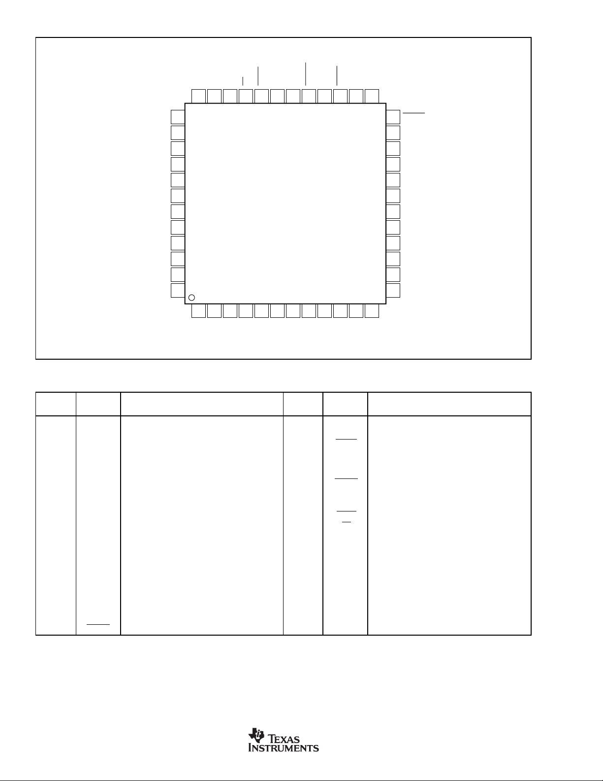
PIN CONFIGURATION
Top View TQFP
AGND
V
REFOUT
V
V
D0
D1
D2
D3
D4
D5
D6
D7
REF+
REF–
OUTDIN
D
SCLKCSDRDY
DVDDDGND
DSYNC
36 35 34 33 32 31 30 29 28 27 26
37
38
39
40
41
42
ADS1217
43
44
45
46
47
48
12345678910112512
0
1
2
3
4
5
IN
IN
IN
A
A
AV
DD
AGND
IN
IN
A
IN
A
A
A
POL
6
IN
A
PDWN
7
IN
A
OUTXIN
X
INCOM
A
AGND
24
23
22
21
20
19
18
17
16
15
14
13
RESET
BUFEN
DGND
DGND
DGND
DGND
DGND
R
DAC
IDAC2
IDAC1
V
RCAP
AV
DD
PIN DESCRIPTIONS
PIN
NUMBER NAME DESCRIPTION
1AV
DD
2 AGND Analog Ground
3A
4A
5A
6A
7A
8A
9A
10 A
11 A
IN
IN
IN
IN
IN
IN
IN
IN
INCOM
12 AGND Analog Ground
13 AV
14 V
DD
RCAP
15 IDAC1 Current DAC1 Output
16 IDAC2 Current DAC2 Output
17 R
DAC
18-22 DGND Digital Ground
23 BUFEN Buffer Enable Input
24 RESET Active LOW, resets the entire chip.
Analog Power Supply
0 Analog Input 0
1 Analog Input 1
2 Analog Input 2
3 Analog Input 3
4 Analog Input 4
5 Analog Input 5
6 Analog Input 6
7 Analog Input 7
Analog Input Common
Analog Power Supply
V
Bypass Capacitor
REFOUT
Current DAC Resistor
PIN
NUMBER NAME DESCRIPTION
25 X
26 X
IN
OUT
Clock Input
Clock Output, used with crystal or resonator.
27 PDWN Active LOW. Power Down. The power-down
function shuts down the analog and digital
circuits.
28 POL Serial Clock Polarity Input
29 DSYNC Active LOW, Synchronization Control Input
30 DGND Digital Ground
31 DV
DD
Digital Power Supply
32 DRDY Active LOW, Data Ready Output
33 CS Active LOW, Chip Select Input
34 SCLK Serial Clock, Schmitt Trigger
35 D
36 D
IN
OUT
Serial Data Input, Schmitt Trigger
Serial Data Output
37-44 D0-D7 Digital I/O 0-7
45 AGND Analog Ground
46 V
47 V
48 V
REFOUT
REF+
REF–
Voltage Reference Output
Positive Differential Reference Input
Negative Differential Reference Input
6
www.ti.com
ADS1217
SBAS260B
Page 7
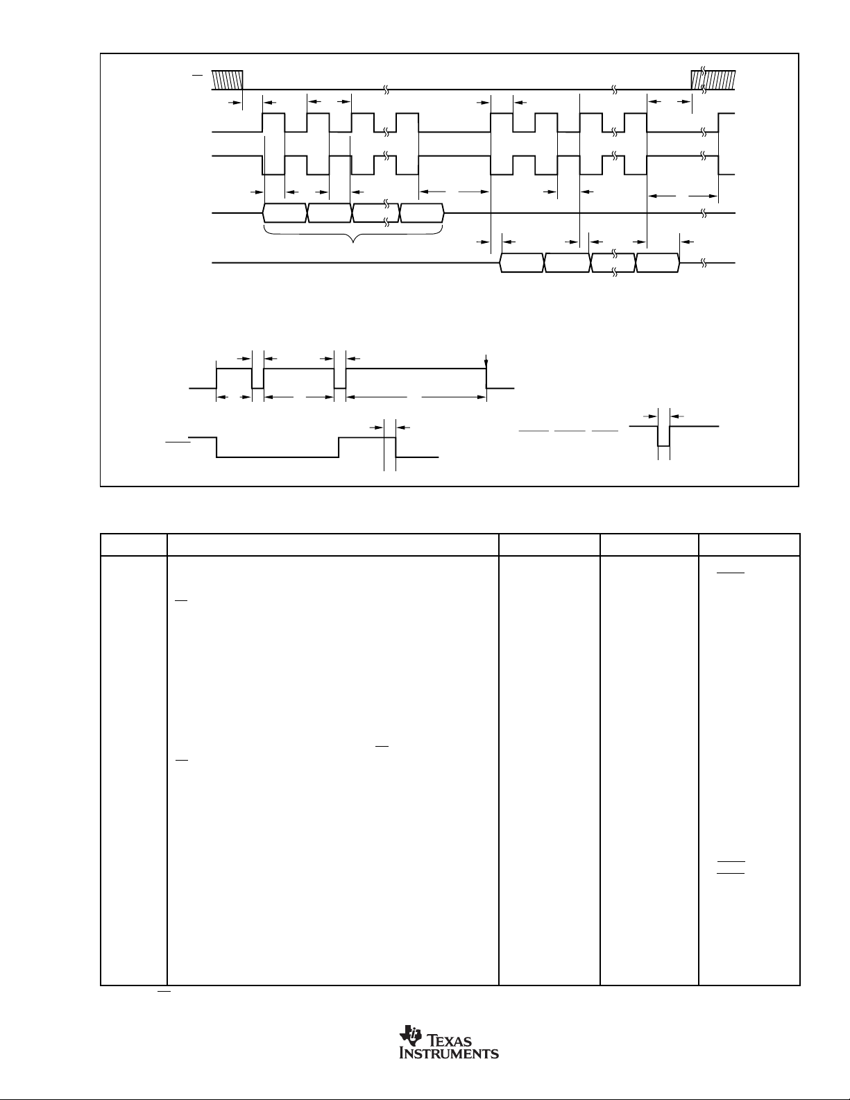
TIMING DIAGRAMS
CS
SCLK
(POL = 0)
SCLK
(POL = 1)
D
IN
t
3
t
4
MSB
t
1
t
5
t
2
t
6
t
2
t
10
t
11
LSB
t
D
OUT
(Command or Command and Data)
7
MSB
t
8
(1)
LSB
t
9
(1)
NOTE: (1) Bit Order = 0.
SCLK Reset Waveform
ADS1217
Resets On
Falling Edge
t
13
t
13
SCLK
t
12
t
14
t
15
t
t
17
RESET, DSYNC, PDWN
16
DRDY
TIMING CHARACTERISTICS
SPEC DESCRIPTION MIN MAX UNITS
t
1
t
2
t
3
t
4
t
5
t
6
(2)
t
7
(2)
t
8
t
9
t
10
t
11
t
12
t
13
t
14
t
15
t
16
t
17
NOTES: (1) CS may be tied LOW. (2) Load = 20pF.
SCLK Period 4t
3 DRDY Periods
SCLK Pulse Width, HIGH and LOW 200 ns
CS LOW to First SCLK Edge; Setup Time
(1)
0ns
DIN Valid to SCLK Edge; Setup Time 50 ns
Valid DIN to SCLK Edge; Hold Time 50 ns
Delay Between Last SCLK Edge for DIN and First SCLK
Edge for D
RDATA, RDATAC, RREG, WREG, RRAM, WRAM 50 t
OUT
:
CSREG, CSRAMX, CSRAM 200 t
CSARAM, CSARAMX 1100 t
SCLK Edge to Valid New D
SCLK Edge to D
Last SCLK Edge to D
NOTE: D
OUT
, Hold Time 0 ns
OUT
Tri-State 6 10 t
OUT
goes tri-state immediately when CS goes HIGH.
OUT
50 ns
CS LOW Time After Final SCLK Edge 0 ns
Final SCLK Edge of One Op Code Until First Edge SCLK
of Next Command:
RREG, WREG, RRAM, WRAM, CSRAMX, CSARAMX, t
CSRAM, CSARAM, CSREG, DSYNC, SLEEP, RDATA,
RDATAC, STOPC 4 t
CREG, CRAM 220 t
CREGA 1600 t
SELFGCAL, SELFOCAL, SYSOCAL, SYSGCAL 7 DRDY Periods
SELFCAL 14 DRDY Periods
RESET (Input pin, command, or SCLK pattern) 16 t
300 500 t
5t
550 750 t
1050 1250 t
Pulse Width 4t
Data Not Valid 4 t
OSC
OSC
OSC
OSC
OSC
OSC
OSC
OSC
OSC
OSC
OSC
OSC
OSC
OSC
OSC
OSC
Periods
Periods
Periods
Periods
Periods
Periods
Periods
Periods
Periods
Periods
Periods
Periods
Periods
Periods
Periods
Periods
ADS1217
SBAS260B
www.ti.com
7
Page 8
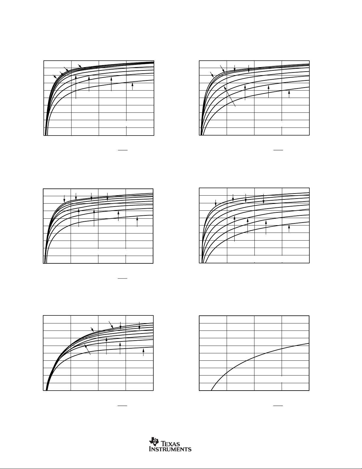
TYPICAL CHARACTERISTICS
AVDD = +5V, DVDD = +5V, f
= 2.4576MHz, PGA = 1, R
OSC
= 150kΩ, f
DAC
= 10Hz, and V
DATA
= +2.5V, unless otherwise specified.
REF
EFFECTIVE NUMBER OF BITS
vs DECIMATION RATIO
22
21
20
PGA1
PGA8
PGA4
PGA2
19
18
17
16
ENOB (rms)
PGA16
PGA32
PGA64
PGA128
15
14
13
Sinc3 Filter, BUFFER OFF
12
0 500 1000 1500 2000
f
Decimation Ratio =
MOD
f
DATA
EFFECTIVE NUMBER OF BITS
vs DECIMATION RATIO
22
21
PGA1
PGA2
PGA4
PGA8
20
19
18
17
16
ENOB (rms)
PGA16
PGA32
PGA64
PGA128
15
14
13
Sinc3 Filter, V
= 1.25V, BUFFER OFF
REF
12
0 500 1000 1500 2000
f
Decimation Ratio =
MOD
f
DATA
EFFECTIVE NUMBER OF BITS
vs DECIMATION RATIO
22
21
PGA2
PGA1
PGA4
PGA8
20
19
18
17
16
ENOB (rms)
15
14
13
PGA16
PGA32
PGA64
Sinc3 Filter, BUFFER ON
PGA128
12
0 500 1000 1500 2000
f
Decimation Ratio =
MOD
f
DATA
EFFECTIVE NUMBER OF BITS
vs DECIMATION RATIO
22
21
PGA1
PGA2
PGA4
PGA8
20
19
18
17
16
ENOB (rms)
15
14
13
12
PGA32
PGA16
Sinc3 Filter, V
PGA64
REF
PGA128
= 1.25V, BUFFER ON
0 500 1000 1500 2000
Decimation Ratio
8
EFFECTIVE NUMBER OF BITS
vs DECIMATION RATIO
22
21
PGA1
PGA2
PGA4
20
19
18
17
16
ENOB (rms)
PGA32
PGA16 PGA64
15
14
13
Sinc2 Filter
12
0 500 1000 1500 2000
f
Decimation Ratio =
f
MOD
DATA
PGA8
PGA128
www.ti.com
EFFECTIVE NUMBER OF BITS vs DECIMATION RATIO
FAST SETTLING FILTER
22
21
20
19
18
17
16
ENOB (rms)
15
14
13
Fast Settling Filter
12
f
f
DATA
1500
MOD
0 500 1000 1500 2000
Decimation Ratio =
ADS1217
SBAS260B
Page 9
TYPICAL CHARACTERISTICS (Cont.)
130
120
110
100
90
80
70
60
50
40
30
20
10
0
COMMON-MODE REJECTION RATIO vs FREQUENCY
Frequency of CM Signal (Hz)
1 10 100 1k 10k 100k
CMRR (dB)
140
120
100
80
60
40
20
0
–20
–40
OFFSET vs TEMPERATURE
Offset (ppm of FS)
Temperature (°C)
–50 0 50 100
PGA128
PGA16
PGA64
PGA1
AVDD = +5V, DVDD = +5V, f
= 2.4576MHz, PGA = 1, R
OSC
= 150kΩ, f
DAC
= 10Hz, and V
DATA
= +2.5V, unless otherwise specified.
REF
0.7
0.6
0.5
0.4
0.3
0.2
Noise (rms, ppm of FS)
0.1
0
–5 –3–4102–1–2345
POWER-SUPPLY REJECTION RATIO vs FREQUENCY
120
110
100
90
80
70
60
50
PSRR (dB)
40
30
20
10
0
110 1k100 10k 100k
NOISE vs INPUT SIGNAL
V
(V)
IN
Frequency of Power Supply (Hz)
1.00010
1.00006
1.00002
0.99998
0.99994
Gain (Normalized)
0.99990
0.99986
ADS1217
–50 –30 10–10 30 50 70 90
SBAS260B
GAIN vs TEMPERATURE
Temperature (°C)
www.ti.com
INTEGRAL NONLINEARITY vs INPUT SIGNAL
6
–40°C
4
2
0
–2
INL (ppm of FS)
–4
–6
–5 –4 –2 –1–3 012345
+25°C
+85°C
(V)
V
IN
9
Page 10

TYPICAL CHARACTERISTICS (Cont.)
AVDD = +5V, DVDD = +5V, f
= 2.4576MHz, PGA = 1, R
OSC
= 150kΩ, f
DAC
= 10Hz, and V
DATA
= +2.5V, unless otherwise specified.
REF
270
CURRENT vs TEMPERATURE
240
I
210
ANALOG
Current (µA)
180
I
DIGITAL
150
–60 –30 0 30 60 90 120
Temperature (°C)
DIGITAL CURRENT
400
350
300
250
200
150
Current (µA)
Normal
2.45MHz
SLEEP
4.91MHz
Normal
4.91MHz
100
50
SLEEP
2.45MHz
0
2.5 3.0 3.5 4.0 4.5 5 5.5
V
(V)
DD
900
800
700
AVDD = 5V, Buffer = ON
Buffer = OFF
600
A/D CURRENT vs PGA
500
(µA)
400
ADC
I
AVDD = 3V, Buffer = ON
Buffer = OFF
300
200
100
0
1824 3216 12864
PGA Setting
5000
HISTOGRAM OF OUTPUT DATA
4000
3000
2000
Number of Occurrences
1000
0
–1.5 –1.0 –0.5 0 0.5 1.0 1.5 2.0
–2.0
ppm of FS
vs LOAD CURRENT
V
2.55
REFOUT
(V)
2.50
REFOUT
V
2.45
–0.5 0 0.5 1.0 1.5 2.0 2.5
Current Load (mA)
V
REFOUT
10
www.ti.com
200
OFFSET DAC: OFFSET vs TEMPERATURE
170
140
110
80
50
20
–10
Offset (ppm of FSR)
–40
–70
–100
–50 –30 10–10 30 50 70 90
Temperature (°C)
ADS1217
SBAS260B
Page 11

TYPICAL CHARACTERISTICS (Cont.)
1.0000
1.000
0.999
0.999
0.998
IDAC
IOUT
vs V
OUT
VDD – V
OUT
(V)
012345
I
OUT
(Normalized)
+85°C
–40°C
+25°C
3000
2000
1000
0
–1000
–2000
–3000
–4000
–5000
–6000
IDAC MATCHING vs TEMPERATURE
IDAC Match (ppm)
Temperature (°C)
–50 –30 10–10 30 50 70 90
AVDD = +5V, DVDD = +5V, f
= 2.4576MHz, PGA = 1, R
OSC
= 150kΩ, f
DAC
= 10Hz, and V
DATA
= +2.5V, unless otherwise specified.
REF
1.00020
1.00016
1.00012
1.00008
1.00004
1.00000
0.99996
0.99992
Normalized Gain
0.99988
0.99984
0.99980
0.99976
–50 –30 10–10 30 50 70 90
1.010
1.005
1.000
OFFSET DAC: GAIN vs TEMPERATURE
Temperature (°C)
IDAC NORMALIZED I
vs TEMPERATURE
OUT
(Normalized)
0.995
OUT
I
0.990
0.985
–50 –30 10–10 30 50 70 90
IDAC DIFFERENTIAL NONLINEARITY
(Range = 1, R
0.5
0.4
0.3
0.2
0.1
0
–0.1
DNL (LSB)
–0.2
ADS1217
–0.3
–0.4
–0.5
0 25532 64 96 128 160 192 224
SBAS260B
Temperature (°C)
= 150kΩ, V
DAC
IDAC Code
REF
= 2.5V)
www.ti.com
IDAC INTEGRAL NONLINEARITY
0.5
(Range = 1, R
= 150kΩ, V
DAC
0.4
0.3
0.2
0.1
0
–0.1
INL (LSB)
–0.2
–0.3
–0.4
–0.5
0 25532 64 96 128 160 192 224
IDAC Code
REF
= 2.5V)
11
Page 12

OVERVIEW
INPUT MULTIPLEXER
The input multiplexer (mux) provides for any combination of
differential inputs to be selected on any of the input channels,
as shown in Figure 1. If channel 1 is selected as the positive
differential input channel, any other channel can be selected
as the negative differential input channel. With this method,
it is possible to have up to eight fully differential input
channels.
In addition, current sources are supplied that will source or
sink current to detect open or short circuits on the pins.
A
0
IN
BURNOUT CURRENT SOURCES
When the Burnout bit is set in the ACR configuration register,
two current sources are enabled. The current source on the
positive input channel sources approximately 2µA of current.
The current source on the negative input channel sinks approximately 2µA. This allows for the detection of an open circuit
(full-scale reading) or short circuit (0V differential reading) on
the selected input differential pair.
INPUT BUFFER
The input impedance of the ADS1217 without the buffer
is 10MΩ/PGA. With the buffer enabled, the input voltage range
is reduced and the analog power-supply current is higher. The
buffer is controlled by ANDing the state of the buffer pin with
the state of the BUFFER bit in the ACR register. See Application Report
(SBAA090) for more information.
Input Currents for High-Resolution ADCs
1
A
A
IN
A
IN
AIN3
A
IN
AIN5
A
IN
A
IN
INCOM
2
4
6
7
AV
DD
Burnout Current Source On
A
IN+
A
IN–
Burnout Current Source On
AGND
IDAC1
FIGURE 1. Input Multiplexer Configuration.
TEMPERATURE SENSOR
An on-chip diode provides temperature sensing capability.
When the configuration register for the input MUX is set to all
1s, the diode is connected to the input of the A/D converter.
All other channels are open. The anode of the diode is
connected to the positive input of the A/D converter, and the
cathode of the diode is connected to negative input of the
A/D converter. The output of IDAC1 is connected to the
anode to bias the diode and the cathode of the diode is also
connected to ground to complete the circuit.
In this mode, the output of IDAC1 is also connected to the
output pin, so some current may flow into an external load
from IDAC1, rather than the diode. See Application Report
Measuring Temperature with the ADS1216, ADS1217, or
ADS1218
(SBAA073) for more information.
IDAC1 AND IDAC2
The ADS1217 has two 8-bit current output DACs that can
be controlled independently. The output current is set with
R
, the range select bits in the ACR register, and the
DAC
8-bit digital value in the IDAC register. The output
current = (V
V
REFOUT
= 2.5V and R
REF
/8R
DAC
RANGE–1
) (2
= 150kΩ, the full-scale output can
DAC
) (DAC CODE). With
be selected to be 0.5, 1, or 2mA. The compliance voltage
range is AGND to within 1V of AV
. When the internal
DD
voltage reference of the ADS1217 is used, it is the reference for the IDAC. An external reference may be used for
the IDACs by disabling the internal reference and tying the
external reference input to the V
REFOUT
pin.
PGA
The PGA can be set to gains of 1, 2, 4, 8, 16, 32, 64, or 128.
Using the PGA can improve the effective resolution of the A/D
converter. For instance, with a PGA of 1 on a 10V full-scale
range, the A/D converter can resolve to 2µV. With a PGA of
128 on a 80mV full-scale range, the A/D converter can resolve
to 150nV.
PGA OFFSET DAC
The input to the PGA can be shifted by half the full-scale input
range of the PGA by using the ODAC register. The ODAC
(Offset DAC) register is an 8-bit value; the MSB is the sign and
the seven LSBs provide the magnitude of the offset. Using the
ODAC does not reduce the performance of the A/D converter.
See Application Report
The Offset DAC
(SBAA077) for more
information.
MODULATOR
The modulator is a single-loop, 2nd-order system. The modulator runs at a clock speed (f
external clock (f
). The frequency division is determined by
OSC
the SPEED bit in the setup register.
SPEED BIT f
0f
1f
) that is derived from the
MOD
MOD
/128
OSC
/ 256
OSC
12
www.ti.com
ADS1217
SBAS260B
Page 13

VOLTAGE REFERENCE INPUT
The ADS1217 uses a differential voltage reference input.
The input signal is measured against the differential voltage
V
≡ (V
REF
2.5V. For AV
REF+
) – (V
= 3V, V
DD
). For AVDD = 5V, V
REF–
is typically 1.25V. Due to the
REF
is typically
REF
sampling nature of the modulator, the reference input current
increases with higher modulator clock frequency (f
MOD
) and
higher PGA settings.
ON-CHIP VOLTAGE REFERENCE
A selectable voltage reference (1.25V or 2.5V) is available for
supplying the voltage reference input. To use, connect V
to AGND and V
REF+
to V
. The enabling and voltage
REFOUT
REF–
selection are controlled through bits REF EN and REF HI in
the setup register. The 2.5V reference requires AV
When using the on-chip voltage reference, the V
= 5V.
DD
REFOUT
pin
should be bypassed with a 0.1µF capacitor to AGND.
V
PIN
RCAP
This pin provides a bypass cap for noise filtering on internal
V
circuitry only. As this is a sensitive pin, place the
REF
capacitor as close as possible and avoid any resistive loading. The recommended capacitor is a 0.001µF ceramic cap.
If an external V
is used, this pin can be left unconnected.
REF
CLOCK GENERATOR
The clock source for the ADS1217 can be provided from a
crystal, oscillator, or external clock. When the clock source is
a crystal, external capacitors must be provided to ensure startup and a stable clock frequency; see Figure 2 and Table I.
X
C
Crystal
C
IN
1
X
OUT
2
complete both an offset and gain calibration. Self-gain calibration is optimized for PGA gains less than 8. When using
higher gains, system gain calibration is recommended.
For system calibration, the appropriate signal must be
applied to the inputs. The system offset command requires a
“zero” differential input signal. It then computes an offset that
will nullify offset in the system. The system gain command
requires a positive “full-scale” differential input signal. It then
computes a value to nullify gain errors in the system. Each of
these calibrations will take seven t
periods to complete.
DATA
Calibration must be performed after power on, a change in
decimation ratio, or a change of the PGA. For operation with
a reference voltage greater than (AV
– 1.5V), the buffer
DD
must also be turned off during calibration.
At the completion of calibration, the
DRDY
signal goes LOW,
which indicates the calibration is finished and valid data is
available. See Application Report
Register Value Generation for the ADS121x Series
Calibration Routine and
(SBAA099)
for more information.
DIGITAL FILTER
The Digital Filter can use either the fast settling, sinc2, or
3
sinc
filter, as shown in Figure 3. In addition, the Auto mode
changes the sinc filter after the input channel or PGA is
changed. When switching to a new channel, it will use the
fast settling filter; It will then use the sinc
3
sinc
filter. This combines the low-noise advantage of the
3
sinc
filter with the quick response of the fast settling time
filter. See Figure 4 for the frequency response of each filter.
When using the fast setting filter, select a decimation value
set by the DEC0 and M/DEC1 registers that is evenly
divisible by four for the best gain accuracy. For example,
choose 260 rather than 261.
Adjustable Digital Filter
3
Sinc
2
followed by the
FIGURE 2. Crystal Connection.
CLOCK PART
SOURCE FREQUENCY C
Crystal 2.4576 0-20pF 0-20pF ECS, ECSD 2.45 - 32
Crystal 4.9152 0-20pF 0-20pF ECS, ECSL 4.91
Crystal 4.9152 0-20pF 0-20pF ECS, ECSD 4.91
Crystal 4.9152 0-20pF 0-20pF CTS, MP 042 4M9182
C
1
2
NUMBER
TABLE I. Typical Clock Sources.
CALIBRATION
The offset and gain errors in the ADS1217, or the complete
system, can be reduced with calibration. Internal calibration
of the ADS1217 is called self calibration. This is handled with
three commands. One command does both offset and gain
calibration. There is also a gain calibration command and an
offset calibration command. Each calibration process takes
seven t
periods to complete. It takes 14 t
DATA
DATA
periods to
ADS1217
SBAS260B
www.ti.com
Modulator
Output
FILTER SETTLING TIME
FILTER (Conversion Cycles)
3
Sinc
2
Sinc
Fast 1
AUTO MODE FILTER SELECTION
CONVERSION CYCLE
1234+
Fast Sinc
2
Sinc
Fast Settling
2
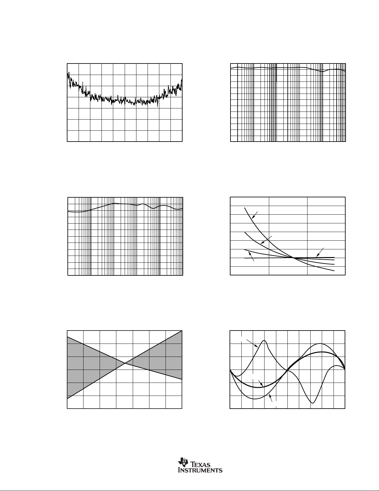
FIGURE 3. Filter Step Responses.
SETTLING TIME
3
2
3
Sinc
Data Out
3
Sinc
13
Page 14
SINC3 FILTER RESPONSE
0
(–3dB = 0.262 • f
DATA
(1)
= 15.76Hz)
SINC2 FILTER RESPONSE
0
(–3dB = 0.318 • f
DATA
(1)
= 19.11Hz)
–20
–40
–60
Gain (dB)
–80
–100
–120
0 30 12060 90 150 180 210 240 270 300
Frequency (Hz)
0
–20
–40
–60
Gain (dB)
–80
–100
–120
0
NOTE: (1) f
30 12060 90 150 180 210 240 270 300
= 60Hz.
DATA
–20
–40
–60
Gain (dB)
–80
–100
–120
0 30 12060 90 150 180 210 240 270 300
FAST SETTLING FILTER RESPONSE
(–3dB = 0.469 • f
Frequency (Hz)
= 28.125Hz)
DATA
Frequency (Hz)
(1)
FIGURE 4. Filter Frequency Responses.
DIGITAL I/O INTERFACE
The ADS1217 has eight pins dedicated for digital I/O. The
default power-up condition for the digital I/O pins are as inputs.
All of the digital I/O pins are individually configurable as inputs
or outputs. They are configured through the DIR control register. The DIR register defines whether the pin is an input or
output, and the DIO register defines the state of the digital
output. When the digital I/O are configured as inputs, DIO is
used to read the state of the pin. If the digital I/O are not used,
either 1) configure as outputs; or, 2) leave as inputs and tie to
ground, this prevents excess power dissipation.
SERIAL PERIPHERAL INTERFACE
The Serial Peripheral Interface (SPI) allows a controller to
communicate synchronously with the ADS1217. The ADS1217
operates in slave only mode.
Chip Select (CS)
The chip select (CS) input of the ADS1217 must be externally asserted before a master device can exchange data
with the ADS1217.
transaction.
CS
must be LOW for the duration of the
CS
can be tied low.
Serial Clock (SCLK)
SCLK, a Schmitt Trigger input, clocks data transfer on the D
input and D
ADS1217, multiple bits of data may be transferred back-to-
output. When transferring data to or from the
OUT
back with no delay in SCLKs or toggling of
CS
. Make sure
to avoid glitches on SCLK as they can cause extra shifting of
the data.
Polarity (POL)
The serial clock polarity is specified by the POL input. When
SCLK is active HIGH, set POL HIGH. When SCLK is active
LOW, set POL LOW.
DATA READY
The
DRDY
output is used as a status signal to indicate when
data is ready to be read from the ADS1217.
DRDY
goes LOW
when new data is available. It is reset HIGH when a read
operation from the data register is complete. It also goes HIGH
prior to the updating of the output register to indicate when not
to read from the device to ensure that a data read is not
attempted while the register is being updated.
DSYNC OPERATION
DSYNC is used to provide for synchronization of the A/D
conversion with an external event. Synchronization can be
achieved either through the
command. When the
DSYNC
reset on the falling edge of
IN
reset until
DSYNC
is taken HIGH. Synchronization occurs on
the next rising edge of the system clock after
taken HIGH.
DSYNC
pin or the DSYNC
pin is used, the filter counter is
DSYNC
. The modulator is held in
DSYNC
is
14
www.ti.com
ADS1217
SBAS260B
Page 15

When the DSYNC command is sent, the filter counter is reset
on the edge of the last SCLK on the DSYNC command. The
modulator is held in reset until the next edge of SCLK is
detected. Synchronization occurs on the next rising edge of
the system clock after the first SCLK after the DSYNC
command. After a DSYNC operation,
DRDY
is held HIGH
until valid data is ready.
RESET
There are three methods to reset the ADS1217: the
input, the RESET command, and a special SCLK input pattern. When using the
RESET
input, take it LOW to force a
reset. Make sure to follow the minimum pulse width timing
specifications before taking the
avoid glitches on the
RESET
RESET
input back high. Also,
input as these may cause
accidental resets. The RESET command takes effect after all
8 bits have been shifted into DIN. Afterwards, the reset
releases automatically. The ADS1217 can also be reset with
a special pattern on SCLK, see the Timing Diagram. Reset
occurs on the falling edge of the last SCLK edge in the pattern
(for POL = 0). Afterwards, the reset releases automatically.
RESET
POWER-UP—SUPPLY VOLTAGE RAMP RATE
The power-on reset circuitry was designed to accommodate
digital supply ramp rates as slow as 1V/10ms. To ensure
proper operation, the power supply should ramp monotonically.
Configuration
Registers
16 bytes
SETUP
MUX
ACR
IDAC1
IDAC2
ODAC
DIO
DIR
DEC0
M/DEC1
OCR0
OCR1
OCR2
FSR0
FSR1
FSR2
RAM
128 Bytes
Bank 0
16 bytes
Bank 2
16 bytes
Bank 7
16 bytes
MEMORY
Two types of memory are used on the ADS1217: registers
and RAM. 16 registers directly control the various functions
(PGA, DAC value, Decimation Ratio, etc.) and can be directly
read or written. Collectively, the registers contain all the
information needed to configure the part, such as data
format, mux settings, calibration settings, decimation ratio,
etc. Additional registers, such as output data, are accessed
through dedicated instructions.
REGISTER BANK TOPOLOGY
The operation of the device is set up through individual
registers. The set of the 16 registers required to configure the
device is referred to as a Register Bank, as shown in Figure 5.
Reads and Writes to Registers and RAM occur on a byte
basis. However, copies between registers and RAM occurs
on a bank basis. The RAM is independent of the Registers;
that is, the RAM can be used as general-purpose RAM.
The ADS1217 supports any combination of eight analog
inputs. With this flexibility, the device could easily support
eight unique configurations—one per input channel. In order
to facilitate this type of usage, eight separate register banks
are available. Therefore, each configuration could be written
once and recalled as needed without having to serially
retransmit all the configuration data. Checksum commands
are also included, which can be used to verify the integrity of
RAM.
FIGURE 5. Memory Organization.
The RAM provides eight “banks”, with a bank consisting of
16 bytes. The total size of the RAM is 128 bytes. Copies
between the registers and RAM are performed on a bank
basis. Also, the RAM can be directly read or written through
the serial interface on power-up. The banks allow separate
storage of settings for each input.
The RAM address space is linear, therefore accessing RAM
is done using an auto-incrementing pointer. Access to RAM
in the entire memory map can be done consecutively without having to address each bank individually. For example,
if you were currently accessing bank 0 at offset 0F
(the last
H
location of bank 0), the next access would be bank 1 and
offset 00
around to bank 0 and Offset 00
. Any access after bank 7 and offset 0FH will wrap
H
.
H
Although the Register Bank memory is linear, the concept of
addressing the device can also be thought of in terms of
bank and offset addressing. Looking at linear and bank
addressing syntax, we have the following comparison: in the
linear memory map, the address 14
1 and offset 04
. Simply stated, the most significant four bits
H
is equivalent to bank
H
represent the bank, and the least significant four bits represent the offset. The offset is equivalent to the register
address for that bank of memory.
ADS1217
SBAS260B
www.ti.com
15
Page 16

REGISTER MAP
ADDRESS REGISTER BIT 7 BIT 6 BIT 5 BIT 4 BIT 3 BIT 2 BIT 1 BIT 0
00
H
01
H
02
H
03
H
04
H
05
H
06
H
07
H
08
H
09
H
0A
H
0B
H
0C
H
0D
H
0E
H
0F
H
TABLE II. Registers.
SETUP ID ID ID SPEED REF EN REF HI BUF EN BIT ORDER
MUX PSEL3 PSEL2 PSEL1 PSEL0 NSEL3 NSEL2 NSEL1 NSEL0
ACR BOCS IDAC2R1 IDAC2R0 IDAC1R1 IDAC1R0 PGA2 PGA1 PGA0
IDAC1 IDAC1_7 IDAC1_6 IDAC1_5 IDAC1_4 IDAC1_3 IDAC1_2 IDAC1_1 IDAC1_0
IDAC2 IDAC2_7 IDAC2_6 IDAC2_5 IDAC2_4 IDAC2_3 IDAC2_2 IDAC2_1 IDAC2_0
ODAC SIGN OSET_6 OSET_5 OSET_4 OSET_3 OSET_2 OSET_1 OSET_0
DIO DIO_7 DIO_6 DIO_5 DIO_4 DIO_3 DIO_2 DIO_1 DIO_0
DIR DIR_7 DIR_6 DIR_5 DIR_4 DIR_3 DIR_2 DIR_1 DIR_0
DEC0 DEC07 DEC06 DEC05 DEC04 DEC03 DEC02 DEC01 DEC00
M/DEC1 DRDY U/B SMODE1 SMODE0 Reserved DEC10 DEC09 DEC08
OCR0 OCR07 OCR06 OCR05 OCR04 OCR03 OCR02 OCR01 OCR00
OCR1 OCR15 OCR14 OCR13 OCR12 OCR11 OCR10 OCR09 OCR08
OCR2 OCR23 OCR22 OCR21 OCR20 OCR19 OCR18 OCR17 OCR16
FSR0 FSR07 FSR06 FSR05 FSR04 FSR03 FSR02 FSR01 FSR00
FSR1 FSR15 FSR14 FSR13 FSR12 FSR11 FSR10 FSR09 FSR08
FSR2 FSR23 FSR22 FSR21 FSR20 FSR19 FSR18 FSR17 FSR16
DETAILED REGISTER DEFINITIONS
SETUP (Address 00H) Setup Register
Reset Value = iii01110
bit 7 bit 6 bit 5 bit 4 bit 3 bit 2 bit 1 bit 0
ID ID ID SPEED REF EN REF HI BUF EN
bit 7-5 Factory Programmed Bits
bit 4 SPEED: Modulator Clock Speed
0 : f
1 : f
bit 3 REF EN: Internal Voltage Reference Enable
0 = Internal Voltage Reference Disabled
1 = Internal Voltage Reference Enabled (default)
bit 2 REF HI: Internal Reference Voltage Select
0 = Internal Reference Voltage = 1.25V
1 = Internal Reference Voltage = 2.5V (default)
bit 1 BUF EN: Buffer Enable
0 = Buffer Disabled
1 = Buffer Enabled (default)
bit 0 BIT ORDER: Set Order Bits are Transmitted
0 = Most Significant Bit Transmitted First (default)
1 = Least Significant Bit Transmitted First
Data is always shifted into the part most significant
bit first. Data is always shifted out of the part most
significant byte first. This configuration bit only controls the bit order within the byte of data that is
shifted out.
MOD
MOD
= f
= f
OSC
OSC
/128 (default)
/256
BIT ORDER
MUX (Address 01H) Multiplexer Control Register
Reset Value = 01
bit 7 bit 6 bit 5 bit 4 bit 3 bit 2 bit 1 bit 0
PSEL3 PSEL2 PSEL1 PSEL0 NSEL3 NSEL2 NSEL1 NSEL0
H
bit 7-4 PSEL3: PSEL2: PSEL1: PSEL0: Positive Channel
Select
0000 = AIN0 (default)
0001 = AIN1
0010 = AIN2
0011 = AIN3
0100 = AIN4
0101 = AIN5
0110 = AIN6
0111 = AIN7
1xxx = AINCOM (except when all bits are 1s)
1111 = Temperature Sensor Diode
bit 3-0 NSEL3: NSEL2: NSEL1: NSEL0: Negative Channel
Select
0000 = AIN0
0001 = AIN1 (default)
0010 = AIN2
0011 = AIN3
0100 = AIN4
0101 = AIN5
0110 = AIN6
0111 = AIN7
1xxx = AINCOM (except when all bits are 1s)
1111 = Temperature Sensor Diode
16
www.ti.com
ADS1217
SBAS260B
Page 17

ACR (Address 02H) Analog Control Register
Reset Value = 00
bit 7 bit 6 bit 5 bit 4 bit 3 bit 2 bit 1 bit 0
BOCS IDAC2R1 IDAC2R0 IDAC1R1 IDAC1R0 PGA2 PGA1 PGA0
H
ODAC (Address 05H) Offset DAC Setting
Reset Value = 00
bit 7 bit 6 bit 5 bit 4 bit 3 bit 2 bit 1 bit 0
SIGN OSET6 OSET5 OSET4 OSET3 OSET2 OSET1 OSET0
H
bit 7 BOCS: Burnout Current Source
0 = Disabled (default)
1 = Enabled
IDAC Current =
V
REF
8
R
DAC
(
RANGE
2
1
−
DACCode
(
)
)
bit 6-5 IDAC2R1: IDAC2R0: Full-Scale Range Select for
IDAC2
00 = Off (default)
01 = Range 1
10 = Range 2
11 = Range 3
bit 4-3 IDAC1R1: IDAC1R0: Full-Scale Range Select for
IDAC1
00 = Off (default)
01 = Range 1
10 = Range 2
11 = Range 3
bit 2-0 PGA2: PGA1: PGA0: Programmable Gain Amplifier
Gain Selection
000 = 1 (default)
001 = 2
010 = 4
011 = 8
100 = 16
101 = 32
110 = 64
111 = 128
IDAC1 (Address 03
Reset Value = 00
bit 7 bit 6 bit 5 bit 4 bit 3 bit 2 bit 1 bit 0
IDAC1_7 IDAC1_6 IDAC1_5 IDAC1_4 IDAC1_3 IDAC1_2 IDAC1_1 IDAC1_0
) Current DAC 1
H
H
The DAC code bits set the output of DAC1 from 0 to fullscale. The value of the full-scale current is set by this Byte,
V
, R
REF
, and the DAC1 range bits in the ACR register.
DAC
bit 7 Offset Sign
0 = Positive
1 = Negative
bit 6-0 Offset =
V
PGA
REF
•
Code
127
NOTE: The offset must be used after calibration or the
calibration will notify the effects.
DIO (Address 06
Reset Value = 00
bit 7 bit 6 bit 5 bit 4 bit 3 bit 2 bit 1 bit 0
DIO7 DIO6 DIO5 DIO4 DIO3 DIO2 DIO1 DIO0
) Digital I/O
H
H
A value written to this register will appear on the digital
I/O pins if the pin is configured as an output in the DIR
register. Reading this register will return the value of the
digital I/O pins.
DIR (Address 07
Reset Value = FF
bit 7 bit 6 bit 5 bit 4 bit 3 bit 2 bit 1 bit 0
DIR7 DIR6 DIR5 DIR4 DIR3 DIR2 DIR1 DIR0
) Direction control for digital I/O
H
H
Each bit controls whether the Digital I/O pin is an output
(= 0) or input (= 1). The default power-up state is as inputs.
DEC0 (Address 08H) Decimation Register
(Least Significant 8 bits)
Reset Value = 80
bit 7 bit 6 bit 5 bit 4 bit 3 bit 2 bit 1 bit 0
DEC07 DEC06 DEC05 DEC04 DEC03 DEC02 DEC01 DEC00
H
The decimation value is defined with 11 bits for a range of 20
to 2047. This register is the least significant 8 bits. The 3
most significant bits are contained in the M/DEC1 register.
The default data rate is 10Hz with a 2.4576MHz crystal.
IDAC2 (Address 04H) Current DAC 2
Reset Value = 00
bit 7 bit 6 bit 5 bit 4 bit 3 bit 2 bit 1 bit 0
IDAC2_7 IDAC2_6 IDAC2_5 IDAC2_4 IDAC1_3 IDAC1_2 IDAC1_1 IDAC1_0
H
The DAC code bits set the output of DAC2 from 0 to fullscale. The value of the full-scale current is set by this Byte,
V
, R
REF
, and the DAC2 range bits in the ACR register.
DAC
ADS1217
SBAS260B
www.ti.com
17
Page 18

M/DEC1 (Address 09H) Mode and Decimation Register
Reset Value = 07
bit 7 bit 6 bit 5 bit 4 bit 3 bit 2 bit 1 bit 0
DRDY U/B SMODE1 SMODE0 Reserved DEC10 DEC09 DEC08
H
bit 7 DRDY: Data Ready (Read Only)
This bit duplicates the state of the DRDY pin.
bit 6 U/B: Data Format
0 = Bipolar (default)
1 = Unipolar
U/B ANALOG INPUT DIGITAL OUTPUT
0 Zero 0x000000
1 Zero 0x000000
+FS 0x7FFFFF
–FS 0x800000
+FS 0xFFFFFF
–FS 0x000000
bit 5-4 SMODE1: SMODE0: Settling Mode
00 = Auto (default)
01 = Fast Settling filter
10 = Sinc
11 = Sinc
2
filter
3
filter
bit 2-0 DEC10: DEC09: DEC08: Most Significant Bits of
the Decimation Value
OCR2 (Address 0CH) Offset Calibration Coefficient
(Most Significant Byte)
Reset Value = 00
bit 7 bit 6 bit 5 bit 4 bit 3 bit 2 bit 1 bit 0
OCR23 OCR22 OCR21 OCR20 OCR19 OCR18 OCR17 OCR16
H
FSR0 (Address 0DH) Full-Scale Register
(Least Significant Byte)
Reset Value = 24
bit 7 bit 6 bit 5 bit 4 bit 3 bit 2 bit 1 bit 0
FSR07 FSR06 FSR05 FSR04 FSR03 FSR02 FSR01 FSR00
H
FSR1 (Address 0EH) Full-Scale Register
(Middle Byte)
Reset Value = 90
bit 7 bit 6 bit 5 bit 4 bit 3 bit 2 bit 1 bit 0
FSR15 FSR14 FSR13 FSR12 FSR011 FSR10 FSR09 FSR08
H
FSR2 (Address 0FH) Full-Scale Register
(Most Significant Byte)
Reset Value = 67
bit 7 bit 6 bit 5 bit 4 bit 3 bit 2 bit 1 bit 0
FSR23 FSR22 FSR21 FSR20 FSR019 FSR18 FSR17 FSR16
H
OCR0 (Address 0A
) Offset Calibration Coefficient
H
(Least Significant Byte)
Reset Value = 00
bit 7 bit 6 bit 5 bit 4 bit 3 bit 2 bit 1 bit 0
OCR07 OCR06 OCR05 OCR04 OCR03 OCR02 OCR01 OCR00
H
OCR1 (Address 0BH) Offset Calibration Coefficient
(Middle Byte)
Reset Value = 00
bit 7 bit 6 bit 5 bit 4 bit 3 bit 2 bit 1 bit 0
OCR15 OCR14 OCR13 OCR12 OCR11 OCR10 OCR09 OCR08
H
18
www.ti.com
ADS1217
SBAS260B
Page 19

COMMAND DEFINITIONS
The commands listed below control the operation of the
ADS1217. Some of the commands are stand-alone commands (e.g., RESET) while others require additional bytes
(e.g., WREG requires command, count, and the data bytes).
Commands that output data require a minimum of four f
OSC
Operands:
n = count (0 to 127)
r = register (0 to 15)
x = don’t care
a = RAM bank address (0 to 7)
cycles before the data is ready (e.g., RDATA).
COMMANDS DESCRIPTION COMMAND BYTE 2ND COMMAND BYTE
RDATA Read Data 0000 0001 (01
RDATAC Read Data Continuously 0000 0011 (03
STOPC Stop Read Data Continuously 0000 1111 (0F
RREG Read from REG Bank
RRAM Read from RAM Bank
CREG Copy REGs to RAM Bank
CREGA Copy REGS to all RAM Banks 0100 1000 (48
WREG Write to REG
WRAM Write to RAM Bank
CRAM Copy RAM Bank
CSRAMX Calc RAM Bank
CSARAMX Calc all RAM Bank Checksum 1101 1000 (D8
CSREG Calc REG Checksum 1101 1111 (DF
CSRAM Calc RAM Bank
CSARAM Calc all RAM Banks Checksum 1110 1000 (E8
SELFCAL Self Cal Offset and Gain 1111 0000 (F0
SELFOCAL Self Cal Offset 1111 0001 (F1
SELFGCAL Self Cal Gain 1111 0010 (F2
SYSOCAL Sys Cal Offset 1111 0011 (F3
SYSGCAL Sys Cal Gain 1111 0100 (F4
WAKEUP Wake Up From Sleep Mode 1111 1011 (FB
DSYNC Sync DRDY 1111 1100 (FC
SLEEP Put in Sleep Mode 1111 1101 (FD
RESET Reset to Power-Up Values 1111 1110 (FE
NOTE: (1) The data received by the A/D converter is always MSB First, the data out format is set by the BIT ORDER bit in ACR reg.
rrrr
aaa
aaa
rrrr
aaa
aaa
to REG 1100 0aaa (CxH) —
aaa
Checksum 1101 0aaa (DxH) —
aaa
Checksum 1110 0aaa (ExH) —
0001 rrrr(1xH) xxxx_nnnn (# of reg-1)
0010 0aaa (2xH) xnnn_nnnn (# of bytes-1)
0100 0aaa (4xH) —
0101 rrrr(5xH) xxxx_nnnn (# of reg-1)
0110 0aaa (6xH) xnnn_nnnn (# of bytes-1)
) —
H
) —
H
) —
H
) —
H
) —
H
) —
H
) —
H
) —
H
) —
H
) —
H
) —
H
) —
H
) —
H
) —
H
) —
H
) —
H
TABLE III. Command Summary.
RDATA Read Data
Description: Read a single 24-bit ADC conversion result. On
completion of read back,
Operands: None
Bytes: 1
Encoding: 0000 0001
Data Transfer Sequence:
DRDY
IN
0000 0001 • • •
D
D
OUT
DRDY
goes HIGH.
(1)
xxxx xxxx xxxx xxxx xxxx xxxx
MSB Mid-Byte LSB
RDATAC Read Data Continuous
Description: Read Data Continuous mode enables the con-
tinuous output of new data on each
eliminates the need to send the Read Data Command on each
DRDY
. This mode may be terminated by either the STOP
Read Continuous command or the RESET command.
Operands: None
Bytes: 1
Encoding: 0000 0011
Data Transfer Sequence:
Command terminated when
or RESET.
(1)
D
D
OUT
DRDY
D
D
OUT
IN
IN
0000 0011 • • •
• • •
uuuu uuuu uuuu uuuu
• • •
MSB Mid-Byte
uuuu uuuu uuuu uuuu uuuu uuuu
MSB Mid-Byte LSB
DRDY
uuuu uuuu
uuuu uuuu
LSB
. This command
equals STOPC
• • •
ADS1217
SBAS260B
NOTE: (1) For wait time, refer to timing specification.
www.ti.com
19
Page 20
STOPC Stop Continuous
D
IN
0100 1000
CREG Copy Registers to RAM Bank
Description: Ends the continuous data output mode.
Operands: None
Bytes: 1
Encoding: 0000 1111
Data Transfer Sequence:
0000 1111
D
IN
RREG Read from Registers
Description: Output the data from up to 16 registers starting
with the register address specified as part of the instruction.
The number of registers read will be one plus the second byte.
If the count exceeds the remaining registers, the addresses will
wrap back to the beginning.
Operands: r, n
Bytes: 2
Encoding: 0001 rrrr xxxx nnnn
Data Transfer Sequence:
Read Two Registers Starting from Register 01
(MUX)
H
Description: Copy the 16 control registers to the RAM bank
specified in the op code. Refer to timing specifications for
command execution time.
Operands: a
Bytes: 1
Encoding: 0100 0aaa
Data Transfer Sequence:
Copy Register Values to RAM Bank 3
0100 0011
D
IN
CREGA Copy Registers to All RAM Banks
Description: Duplicate the 16 control registers to all the RAM
banks. Refer to timing specifications for command execution
time.
Operands: None
Bytes: 1
Encoding: 0100 1000
Data Transfer Sequence:
0001 0001 0000 0001 xxxx xxxx xxxx xxxx
D
IN
D
OUT
• • •
(1)
MUX ACR
RRAM Read from RAM
Description: Up to 128 bytes can be read from RAM starting
at the bank specified in the op code. All reads start at the
address for the beginning of the RAM bank. The number of
bytes to read will be one plus the value of the second byte.
Operands: a, n
Bytes: 2
Encoding: 0010 0aaa xnnn nnnn
Data Transfer Sequence:
Read Two RAM Locations Starting from 20
0010 0010 x000 0001 xxxx xxxx xxxx xxxx
D
IN
D
OUT
• • •
(1)
H
RAM Data
20
H
RAM Data
21
H
WREG Write to Register
Description: Write to the registers starting with the register
specified as part of the instruction. The number of registers that
will be written is one plus the value of the second byte.
Operands: r, n
Bytes: 2
Encoding: 0101 rrrr xxxx nnnn
Data Transfer Sequence:
Write Two Registers Starting from 06
0101 0110 xxxx 0001
D
IN
(DIO)
H
Data for DIO Data for DIR
NOTE: (1) For wait time, refer to timing specification.
20
www.ti.com
ADS1217
SBAS260B
Page 21

WRAM Write to RAM
Description: Write up to 128 RAM locations starting at the
beginning of the RAM bank specified as part of the instruction.
The number of bytes written is RAM is one plus the value of the
second byte.
Operands: a, n
Bytes: 2
Encoding: 0110 0aaa xnnn nnnn
Data Transfer Sequence:
Write to Two RAM Locations starting from 10
H
Calculate the Checksum
CSARAMX for all RAM Banks
Description: Calculate the checksum of all RAM Banks. The
checksum is calculated as a sum of all the bytes with the carry
ignored. The ID,
not included in the checksum.
Operands: None
Bytes: 1
Encoding: 1101 1000
Data Transfer Sequence:
DRDY
, and DIO bits are masked so they are
0110 0001 x000 0001
D
IN
Data for
10
H
Data for
11
H
CRAM Copy RAM Bank to Registers
Description: Copy the selected RAM Bank to the Configura-
tion Registers. This will overwrite all of the registers with the
data from the RAM bank.
Operands: a
Bytes: 1
Encoding: 1100 0aaa
Data Transfer Sequence:
Copy RAM Bank 0 to the Registers
1100 0000
D
IN
CSRAMX Calculate RAM Bank Checksum
Description: Calculate the checksum of the selected RAM
Bank. The checksum is calculated as a sum of all the bytes with
the carry ignored. The ID,
they are not included in the checksum.
Operands: a
Bytes: 1
Encoding: 1101 0aaa
Data Transfer Sequence:
Calculate Checksum for RAM Bank 3
D
IN
D
OUT
DRDY
1101 0011 • • •
, and DIO bits are masked so
(1)
xxxx xxxx
Checksum
D
IN
D
OUT
1101 1000 • • •
(1)
xxxx xxxx
Checksum
Calculate the Checksum
CSREG of Registers
Description: Calculate the checksum of all the registers. The
checksum is calculated as a sum of all the bytes with the carry
ignored. The ID,
DRDY
and DIO bits are masked so they are
not included in the checksum.
Operands: None
Bytes: 1
Encoding: 1101 1111
Data Transfer Sequence:
D
IN
D
OUT
1101 1111 • • •
(1)
xxxx xxxx
Checksum
CSRAM Calculate RAM Bank Checksum
Description: Calculate the checksum of the selected RAM
Bank. The checksum is calculated as a sum of all the bytes with
the carry ignored. All bits are included in the checksum
calculation, there is no masking of bits.
Operands: a
Bytes: 1
Encoding: 1110 0aaa
Data Transfer Sequence:
Calculate Checksum for RAM Bank 2
ADS1217
SBAS260B
NOTE: (1) For wait time, refer to timing specification.
www.ti.com
D
IN
D
OUT
1110 0010 • • •
(1)
xxxx xxxx
Checksum
21
Page 22

Calculate Checksum
D
IN
1111 0010
CSARAM for all RAM Banks
Description: Calculate the checksum of all RAM Banks. The
checksum is calculated as a sum of all the bytes with the carry
ignored. All bits are included in the checksum calculation, there
is no masking of bits.
Operands: None
Bytes: 1
Encoding: 1110 1000
Data Transfer Sequence:
SELFGCAL Gain Self Calibration
Description: Starts the process of self-calibration for gain.
The Full-Scale Register (FSR) is updated with new values after
this operation.
Operands: None
Bytes: 1
Encoding: 1111 0010
Data Transfer Sequence:
D
IN
D
OUT
1110 1000 • • •
(1)
xxxx xxxx
Checksum
SELFCAL Offset and Gain Self Calibration
Description: Starts the process of self calibration. The Offset
Control Register (OCR) and the Full-Scale Register (FSR) are
updated with new values after this operation.
Operands: None
Bytes: 1
Encoding: 1111 0000
Data Transfer Sequence:
1111 0000
D
IN
SELFOCAL Offset Self Calibration
Description: Starts the process of self-calibration for offset.
The Offset Control Register (OCR) is updated after this operation.
Operands: None
Bytes: 1
Encoding: 1111 0001
Data Transfer Sequence:
SYSOCAL System Offset Calibration
Description: Starts the system offset calibration process. For
a system offset calibration the input should be set to 0V
differential, and the ADS1217 computes the OCR register
value that will compensate for offset errors. The Offset Control
Register (OCR) is updated after this operation.
Operands: None
Bytes: 1
Encoding: 1111 0011
Data Transfer Sequence:
1111 0011
D
IN
SYSGCAL System Gain Calibration
Description: Starts the system gain calibration process. For
a system gain calibration, the differential input should be set to
the reference voltage and the ADS1217 computes the FSR
register value that will compensate for gain errors. The FSR is
updated after this operation.
Operands: None
Bytes: 1
Encoding: 1111 0100
Data Transfer Sequence:
1111 0001
D
IN
NOTE: (1) For wait time, refer to timing specification.
22
www.ti.com
D
IN
1111 0100
ADS1217
SBAS260B
Page 23

DSYNC Sync
DRDY
WAKEUP Wakeup From Sleep Mode
Description: Synchronizes the ADS1217 to the serial clock
edge.
Operands: None
Bytes: 1
Encoding: 1111 1100
Data Transfer Sequence:
1111 1100
D
IN
SLEEP Sleep Mode
Description: Puts the ADS1217 into a low power sleep mode.
SCLK must be inactive while in sleep mode. To exit this mode,
issue the WAKEUP command.
Operands: None
Bytes: 1
Encoding: 1111 1101
Data Transfer Sequence:
1111 1101
D
IN
Description: Use this command to wake up from sleep mode.
Operands: None
Bytes: 1
Encoding: 1111 1011
Data Transfer Sequence:
1111 1011
D
IN
RESET Reset to Power-Up Values
Description: Restore the registers to their power-up values.
This command will also stop the Read Continuous mode. It
does not affect the contents of RAM.
Operands: None
Bytes: 1
Encoding: 1111 1110
Data Transfer Sequence:
1111 1110
D
IN
LSB
MSB 0000 0001 0010 0011 0100 0101 0110 0111 1000 1001 1010 1011 1100 1101 1110 1111
0000 x rdata x rdatac x x x x x x x x x x x stopc
0001 rreg rreg rreg rreg rreg rreg rreg rreg rreg rreg rreg rreg rreg rreg rreg rreg
0010 rram rram rram rram rram rram rram rram x x x x x x x x
0011 x x x x x x x x x x x x x x x x
0100 creg creg creg creg creg creg creg creg crega x x x x x x x
0101 wreg wreg wreg wreg wreg wreg wreg wreg wreg wreg wreg wreg wreg wreg wreg wreg
0110 wram wram wram wram wram wram wram wram x x x x x x x x
0111 x x x x x x x x x x x x x x x x
1000 x x x x x x x x x x x x x x x x
1001 x x x x x x x x x x x x x x x x
1010 x x x x x x x x x x x x x x x x
1011 x x x x x x x x x x x x x x x x
1100 cram 0 cram 1 cram 2 cram 3 cram 4 cram 5 cram 6 cram 7 x x x x x x x x
1101 csramx csramx csramx csramx csramx csramx csramx csramx csa x x x x x x
1110 cs cs cs cs cs cs cs cs csa x x x x x x x
1111 self self self sys sys x x x x x x wakeup dsync sleep reset x
x = Reserved
0123456789ABCDEF
01234567
01234567
0123456789ABCDEF
01234567
0 1 2 3 4 5 6 7 ramx csreg
ram 0 ram 1 ram2 ram 3 ram 4 ram 5 ram 6 ram 7 ram
cal ocal gcal ocal gcal
TABLE IV. Command Map.
ADS1217
SBAS260B
www.ti.com
23
Page 24

DEFINITION OF TERMS
Analog Input Voltage—the voltage at any one analog input
relative to AGND.
Analog Input Differential Voltage—given by the following
equation: (A
produced whenever the analog input differential voltage is
positive, while a negative digital output is produced whenever
the differential is negative.
For example, when the converter is configured with a 2.5V
reference and placed in a gain setting of 1, the positive
full-scale output is produced when the analog input differential is 2 • 2.5V. The negative full-scale output is produced
when the differential is 2 • (–2.5V). In each case, the actual
input voltages must remain within the AGND to AV
Conversion Cycle—the term
to a discrete A/D conversion operation, such as that performed by a successive approximation converter. As used
here, a conversion cycle refers to the t
However, each digital output is actually based on the modulator results from several t
) – (A
IN+
). Thus, a positive digital output is
IN–
range.
DD
conversion cycle
time periods.
DATA
usually refers
time period.
DATA
BITS rms BIPOLAR Vrms UNIPOLAR Vrms
4
V
REF
PGA
. •
602
ENOB
10
24 596nV 298nV
22 2.38µV1.19µV
20 9.54µV4.77µV
18 38.1µV 19.1µV
16 153µV 76.4µV
14 610µV 305µV
12 2.44mV 1.22mV
f
—the frequency of the digital output data produced by
DATA
the ADS1217, f
f
f
MOD
DATA
=
DecimationRatio
—the frequency or speed at which the modulator of the
is also referred to as the Data Rate.
DATA
f
MOD OSC
20
=
mfactor DecimationRatio
2
V
REF
PGA
. •
602
ENOB
10
20
f
•
ADS1217 is running. This depends on the SPEED bit as
shown below:
FILTER SETTING MODULATOR RESULTS
2 t
3 t
DATA
DATA
DATA
Time Period
Time Period
Time Period
Fast Settling 1 t
2
Sinc
3
Sinc
Data Rate—the rate at which conversions are completed.
See definition for f
DATA
.
Decimation Ratio—defines the ratio between the output of
the modulator and the output Data Rate. Valid values for the
Decimation Ratio are from 20 to 2047. Larger Decimation
Ratios will have lower noise.
Effective Resolution—the effective resolution of the
ADS1217 in a particular configuration can be expressed in
two different units: bits rms (referenced to output) and Vrms
(referenced to input). Computed directly from the converter’s
output data, each is a statistical calculation. The conversion
from one to the other is shown below.
Effective number of bits
(ENOB) or
effective resolution
is
commonly used to define the usable resolution of the
A/D converter. It is calculated from empirical data taken
directly from the device. It is typically determined by applying
a fixed known signal source to the analog input and computing the standard deviation of the data sample set. The rms
noise defines the ±
σ interval about the sample mean.
The data from the A/D converter is output as codes, which
then can be easily converted to other units, such as ppm or
volts. The equations and table below show the relationship
between bits or codes, ppm, and volts.
ENOB
– log( )
=
ppm
.20602
SPEED BIT f
0f
1f
f
—the frequency of the crystal input signal at the XIN input
OSC
OSC
OSC
MOD
/128
/256
of the ADS1217.
f
—the frequency, or switching speed, of the input sam-
SAMP
pling capacitor. The value is given by one of the following
equations:
PGA SETTING SAMPLING FREQUENCY
f
1, 2, 4, 8
8
16
32
64, 128
f
f
f
f
f
SAMP
SAMP
SAMP
SAMP
SAMP
Filter Selection—the ADS1217 uses a (sinx/x) filter or
=
mfactor
=
mfactor
=
mfactor
16
=
mfactor
16
=
mfactor
OSC
f
2
OSC
f
8
OSC
f
OSC
f
OSC
sinc
filter. There are three different sinc filters that can be selected. A fast settling filter will settle in one t
2
sinc
filter will settle in two cycles and have lower noise. The
3
sinc
will achieve lowest noise and higher number of effective
cycle. The
DATA
bits, but requires three cycles to settle. The ADS1217 will
operate with any one of these filters, or it can operate in an
auto mode, where it will first select the fast settling filter after
a new channel is selected and will then switch to sinc
reading, followed by sinc
3
from then on.
2
for one
24
www.ti.com
ADS1217
SBAS260B
Page 25

Full-Scale Range (FSR)—as with most A/D converters, the
full-scale range of the ADS1217 is defined as the “input”,
which produces the positive full-scale digital output minus the
“input”, which produces the negative full-scale digital output.
The full-scale range changes with gain setting, see Table V.
For example, when the converter is configured with a 2.5V
reference and is placed in a gain setting of 2, the full-scale
range is: 2 • [1.25V (positive full-scale) minus –1.25V (negative full-scale)] = 5V.
Least Significant Bit (LSB) Weight—this is the theoretical
amount of voltage that the differential voltage at the analog
input would have to change in order to observe a change in
the output data of one least significant bit. It is computed as
follows:
Full Scale Range
LSB Weight
−
=
N
2
where N is the number of bits in the digital output.
—the inverse of f
t
DATA
, or the period between each data
DATA
output.
5V SUPPLY ANALOG INPUT
GAIN SETTING FULL-SCALE RANGE INPUT VOLTAGES
1 10V ±5V ±2.5
25V±2.5V ±1.25V
42.5V±1.25V ±0.625V
8 1.25V ±0.625V ±312.5mV
16 0.625V ±312.5mV ±156.25mV
32 312.5mV ±156.25mV ±78.125mV
64 156.25mV ±78.125mV ±39.0625mV
128 78.125mV ±39.0625mV ±19.531mV
NOTES: (1) With a 2.5V reference. (2) The ADS1217 allows common-mode voltage as long as the absolute input voltage on A
AGND or above AV
.
DD
DIFFERENTIAL PGA OFFSET FULL-SCALE DIFFERENTIAL PGA SHIFT
(1)
(2)
RANGE RANGE INPUT VOLTAGES
4V
REF
PGA
GENERAL EQUATIONS
TABLE V. Full-Scale Range versus PGA Setting.
±2V
PGA
IN+
REF
or A
does not go below
IN–
(2)
RANGE
±V
REF
PGA
ADS1217
SBAS260B
www.ti.com
25
Page 26

PACKAGE OPTION ADDENDUM
www.ti.com
11-Oct-2004
PACKAGING INFORMATION
ORDERABLE DEVICE STATUS(1) PACKAGE TYPE PACKAGE DRAWING PINS PACKAGE QTY
ADS1217IPFBR ACTIVE TQFP PFB 48 2000
ADS1217IPFBT ACTIVE TQFP PFB 48 250
(1) The marketing status values are defined as follows:
ACTIVE: Product device recommended for new designs.
LIFEBUY: TI has announced that the device will be discontinued, and a lifetime-buy period is in effect.
NRND: Not recommended for new designs. Device is in production to support existing customers, but TI does not recommend using this part in
a new design.
PREVIEW: Device has been announced but is not in production. Samples may or may not be available.
OBSOLETE: TI has discontinued the production of the device.
Page 27

MECHANICAL DATA
MTQF019A – JANUARY 1995 – REVISED JANUARY 1998
PFB (S-PQFP-G48) PLASTIC QUAD FLATPACK
37
48
1,05
0,95
0,50
36
0,27
0,17
25
24
13
1
5,50 TYP
7,20
SQ
6,80
9,20
SQ
8,80
12
M
0,08
0,05 MIN
Seating Plane
0,13 NOM
Gage Plane
0,25
0°–7°
0,75
0,45
1,20 MAX
NOTES: A. All linear dimensions are in millimeters.
B. This drawing is subject to change without notice.
C. Falls within JEDEC MS-026
0,08
4073176/B 10/96
POST OFFICE BOX 655303 • DALLAS, TEXAS 75265
Page 28

IMPORTANT NOTICE
Texas Instruments Incorporated and its subsidiaries (TI) reserve the right to make corrections, modifications,
enhancements, improvements, and other changes to its products and services at any time and to discontinue
any product or service without notice. Customers should obtain the latest relevant information before placing
orders and should verify that such information is current and complete. All products are sold subject to TI’s terms
and conditions of sale supplied at the time of order acknowledgment.
TI warrants performance of its hardware products to the specifications applicable at the time of sale in
accordance with TI’s standard warranty. Testing and other quality control techniques are used to the extent TI
deems necessary to support this warranty . Except where mandated by government requirements, testing of all
parameters of each product is not necessarily performed.
TI assumes no liability for applications assistance or customer product design. Customers are responsible for
their products and applications using TI components. To minimize the risks associated with customer products
and applications, customers should provide adequate design and operating safeguards.
TI does not warrant or represent that any license, either express or implied, is granted under any TI patent right,
copyright, mask work right, or other TI intellectual property right relating to any combination, machine, or process
in which TI products or services are used. Information published by TI regarding third-party products or services
does not constitute a license from TI to use such products or services or a warranty or endorsement thereof.
Use of such information may require a license from a third party under the patents or other intellectual property
of the third party, or a license from TI under the patents or other intellectual property of TI.
Reproduction of information in TI data books or data sheets is permissible only if reproduction is without
alteration and is accompanied by all associated warranties, conditions, limitations, and notices. Reproduction
of this information with alteration is an unfair and deceptive business practice. TI is not responsible or liable for
such altered documentation.
Resale of TI products or services with statements different from or beyond the parameters stated by TI for that
product or service voids all express and any implied warranties for the associated TI product or service and
is an unfair and deceptive business practice. TI is not responsible or liable for any such statements.
Following are URLs where you can obtain information on other Texas Instruments products and application
solutions:
Products Applications
Amplifiers amplifier.ti.com Audio www.ti.com/audio
Data Converters dataconverter.ti.com Automotive www.ti.com/automotive
DSP dsp.ti.com Broadband www.ti.com/broadband
Interface interface.ti.com Digital Control www.ti.com/digitalcontrol
Logic logic.ti.com Military www.ti.com/military
Power Mgmt power.ti.com Optical Networking www.ti.com/opticalnetwork
Microcontrollers microcontroller.ti.com Security www.ti.com/security
Telephony www.ti.com/telephony
Video & Imaging www.ti.com/video
Wireless www.ti.com/wireless
Mailing Address: Texas Instruments
Post Office Box 655303 Dallas, Texas 75265
Copyright 2004, Texas Instruments Incorporated
 Loading...