

ADS1210
ADS1211
ADS1210
ADS1211
ADS1211
查询ADS1210供应商查询ADS1210供应商
®
24-Bit ANALOG-TO-DIGITAL CONVERTER
FEA TURES
● DELTA-SIGMA A/D CONVERTER
● 23 BITS EFFECTIVE RESOLUTION AT 10Hz
AND 20 BITS AT 1000Hz
● DIFFERENTIAL INPUTS
● PROGRAMMABLE GAIN AMPLIFIER
● FLEXIBLE SPI COMPATIBLE SSI
INTERFACE WITH 2-WIRE MODE
● PROGRAMMABLE CUT-OFF FREQUENCY
UP TO 15.6kHz
● INTERNAL/EXTERNAL REFERENCE
● ON CHIP SELF-CALIBRATION
● ADS1211 INCLUDES 4 CHANNEL MUX
APPLICATIONS
● INDUSTRIAL PROCESS CONTROL
● INSTRUMENTATION
● BLOOD ANALYSIS
● SMART TRANSMITTERS
● PORTABLE INSTRUMENTS
● WEIGH SCALES
● PRESSURE TRANSDUCERS
AGND AVDDREF
OUT
ADS1210
ADS1211
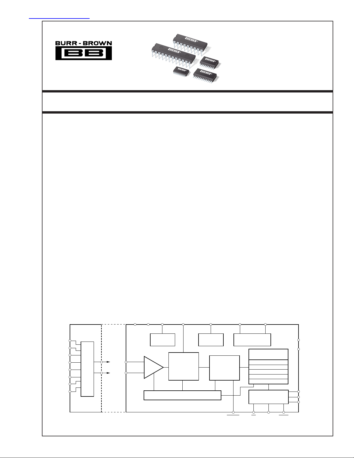
DESCRIPTION
The ADS1210 and ADS1211 are precision, wide
dynamic range, delta-sigma analog-to-digital converters
with 24-bit resolution operating from a single +5V
supply. The differential inputs are ideal for direct
connection to transducers or low level voltage signals. The delta-sigma architecture is used for wide
dynamic range and to guarantee 22 bits of no missing
code performance. An effective resolution of 23 bits
is achieved through the use of a very low-noise input
amplifier at conversion rates up to 10Hz. Effective
resolutions of 20 bits can be maintained up to a
sample rate of 1kHz through the use of the unique
Turbo modulator mode of operation. The dynamic
range of the converters is further increased by providing a low-noise programmable gain amplifier with a
gain range of 1 to 16 in binary steps.
The ADS1210 and ADS1211 are designed for high
resolution measurement applications in smart transmitters, industrial process control, weigh scales, chromatography and portable instrumentation. Both converters include a flexible synchronous serial interface
which is SPI compatible and also offers a two-wire
control mode for low cost isolation.
The ADS1210 is a single channel converter and is
offered in both 18-pin DIP and 18-lead SOIC packages. The ADS1211 includes a 4 channel input multiplexer and is available in 24-pin DIP, 24-lead SOIC,
and 28-lead SSOP packages.
REF
IN
V
BIAS
X
IN
X
OUT
PGA
+2.5V
Reference
Second-Order
∆∑
Modulator
Modulator Control
1P
A
IN
AIN1N
A
2P
IN
AIN2N
A
3P
IN
AIN3N
A
4P
IN
AIN4N
International Airport Industrial Park • Mailing Address: PO Box 11400, Tucson, AZ 85734 • Street Address: 6730 S. Tucson Blvd., Tucson, AZ 85706 • Tel: (520) 746-1111
©
1996 Burr-Brown Corporation PDS-1284E Printed in U.S.A. May, 2000
MUX
ADS1211 Only ADS1210/11
Twx: 910-952-1111 • Internet: http://www.burr-brown.com/ • Cable: BBRCORP • Telex: 066-6491 • FAX: (520) 889-1510 • Immediate Product Info: (800) 548-6132
AINP
A
IN
N
+3.3V Bias
Generator
Third-Order
Digital Filter
Clock Generator
Micro Controller
Instruction Register
Command Register
Data Output Register
Offset Register
Full-Scale Register
Serial Interface
DSYNC CS DRDY
MODE
1 ADS1210, 1211
DGND
DV
DD
SCLK
SDIO
SDOUT
®

SPECIFICATIONS
All specifications T
and external 2.5V reference, unless otherwise specified.
PARAMETER CONDITIONS MIN TYP MAX UNITS
ANALOG INPUT
Input Voltage Range
Input Impedance G = Gain, TMR = Turbo Mode Rate 4/(G • TMR)
Programmable Gain Amplifier User Programmable: 1, 2, 4, 8, or 16 1 16
Input Capacitance 8pF
Input Leakage Current At +25°C550pA
SYSTEMS PERFORMANCE
Resolution 24 Bits
No Missing Codes f
Integral Linearity f
Unipolar Offset Error
Unipolar Offset Drift
Gain Error
Gain Error Drift
Common-Mode Rejection
Normal-Mode Rejection 50Hz, f
Output Noise See Typical Performance Curves
Power Supply Rejection DC, 50Hz, and 60Hz 65 dB
VOLTAGE REFERENCE
Internal Reference (REF
Drift 25 ppm/°C
Noise 50 µVp-p
Load Current Source or Sink 1 mA
Output Impedance 2 Ω
External Reference (REF
Load Current 2.5 µA
V
Output Using Internal Reference 3.15 3.3 3.45 V
BIAS
Drift 50 ppm/°C
Load Current Source or Sink 10mA
DIGITAL INPUT/OUTPUT
Logic Family TTL Compatible CMOS
Logic Level: (all except X
X
Input Levels: V
IN
X
Frequency Range (f
IN
Output Data Rate (f
Data Format User Programmable
SYSTEM CALIBRATION
Offset and Full-Scale Limits V
VFS – | VOS |V
to T
MIN
, AVDD = DVDD = +5V, f
MAX
= 10MHz, programmable gain amplifier setting of 1, Turbo Mode Rate of 1, REF
XIN
disabled,V
OUT
BIAS
disabled,
ADS1210U, P/ADS1211U, P, E
(1)
With V
At T
DATA
DATA
f
= 1000Hz, TMR of 16 ±0.0015 %FSR
(4)
(6)
(4)
(6)
(9)
DATA
At DC, +25°C 100 115 dB
At DC, T
50Hz, f
60Hz, f
60Hz, f
) 2.4 2.5 2.6 V
OUT
) 2.0 3.0 V
IN
)
V
IH
V
IL
V
OH
V
OL
IN
IOH = 2 TTL Loads 2.4 V
IOL = 2 TTL Loads 0.4 V
IH
V
IL
) 0.5 10 MHz
XIN
) User Programmable 2.4 15,625 Hz
DATA
f
XIN
(2)
BIAS
to T
MIN
MAX
= 60Hz 22 Bits
= 60Hz ±0.0015 %FSR
to T
MIN
MAX
(7)
= 50Hz
DATA
DATA
DATA
DATA
= 60Hz
= 50Hz
= 60Hz
(7)
(7)
(7)
IIH = +5µA 2.0 DV
IIL = +5µA –0.3 0.8 V
= 500kHz 0.12 781 Hz
0+5V
–10 +10 V
(3)
MΩ
1nA
See Note 5
1 µV/°C
See Note 5
1 µV/°C
90 115 dB
160 dB
160 dB
100 dB
100 dB
+0.3 V
DD
3.5 DV
–0.3 0.8 V
+0.3 V
DD
Two’s Complement
or Offset Binary
= Full-Scale Differential Voltage
FS
= Offset Differential Voltage
OS
(8)
0.7 • (2 • REFIN)/G
(8)
1.3 • (2 • REFIN)/G
The information provided herein is believed to be reliable; however, BURR-BROWN assumes no responsibility for inaccuracies or omissions. BURR-BROWN assumes
no responsibility for the use of this information, and all use of such information shall be entirely at the user’s own risk. Prices and specifications are subject to change
without notice. No patent rights or licenses to any of the circuits described herein are implied or granted to any third party. BURR-BROWN does not authorize or warrant
any BURR-BROWN product for use in life support devices and/or systems.
®
ADS1210, 1211
2
SPECIFICATIONS (CONT)
All specifications T
and external 2.5V reference, unless otherwise specified.
PARAMETER CONDITIONS MIN TYP MAX UNITS
POWER SUPPLY REQUIREMENTS
Power Supply Voltage 4.75 5.25 V
Power Supply Current:
Analog Current 2mA
Digital Current 3.5 mA
Additional Analog Current with
REF
V
BIAS
Power Dissipation 26 40 mW
TEMPERATURE RANGE
Specified –40 +85 °C
Storage –60 +125 °C
NOTES: (1) In order to achieve the converter’s full-scale range, the input must be fully differential (A
A
P is fixed), then the full scale range is one-half that of the differential range. (2) This range is set with external resistors and V
IN
Other ranges are possible. (3) Input impedance is higher with lower f
of the effective resolution of the converter. Refer to the Typical Performance Curves which apply to the desired mode of operation. (6) Recalibration can remove
these errors. (7) The specification also applies at f
mode rejection test is performed with a 100mV differential input.
to T
MIN
Enabled 1.6 mA
OUT
Enabled No Load 1 mA
, AVDD = DVDD = +5V, f
MAX
= 10MHz, programmable gain amplifier setting of 1, Turbo Mode Rate of 1, REF
XIN
ADS1210U, P/ADS1211U, P, E
TMR of 16 37 60 mW
f
= 2.5MHz 17 mW
XIN
f
= 2.5MHz, TMR of 16 27 mW
XIN
Sleep Mode 11 mW
N = 2 • REFIN – AINP). If the input is single-ended (AINN or
IN
. (4) Applies after calibration. (5) After system calibration, these errors will be of the order
XIN
/i, where i is 2, 3, 4, etc. (8) Voltages at the analog inputs must remain within AGND to AVDD. (9) The common-
DATA
disabled,V
OUT
(as described in the text).
BIAS
BIAS
disabled,
ABSOLUTE MAXIMUM RATINGS
Analog Input: Current................................................ ±100mA, Momentary
AV
DD
AV
DD
DV
DD
AGND to DGND ................................................................................ ±0.3V
REF
Digital Input Voltage to DGND ..................................–0.3V to DV
Digital Output Voltage to DGND ............................... –0.3V to DV
Lead Temperature (soldering, 10s) .............................................. +300°C
Power Dissipation (Any package) .................................................. 500mW
Voltage ................................... AGND –0.3V to AV
to DVDD...........................................................................–0.3V to 6V
to AGND .........................................................................–0.3V to 6V
to DGND.........................................................................–0.3V to 6V
Voltage to AGND............................................–0.3V to AVDD +0.3V
IN
±10mA, Continuous
DD
DD
DD
+0.3V
+0.3V
+0.3V
ELECTROSTATIC
DISCHARGE SENSITIVITY
This integrated circuit can be damaged by ESD. Burr-Brown
recommends that all integrated circuits be handled with appropriate precautions. Failure to observe proper handling and
installation procedures can cause damage.
Electrostatic discharge can cause damage ranging from
performance degradation to complete device failure. BurrBrown Corporation recommends that all integrated circuits be
handled and stored using appropriate ESD protection
methods.
PACKAGE/ORDERING INFORMATION
PACKAGE
DRAWING TEMPERATURE
PRODUCT PACKAGE NUMBER
ADS1210P 18-Pin Plastic DIP 218 –40°C to +85°C
ADS1210U 18-Lead SOIC 219 –40°C to +85°C
ADS1211P 24-Pin Plastic DIP 243 –40°C to +85°C
ADS1211U 24-Lead SOIC 239 –40°C to +85°C
ADS1211E 28-Lead SSOP 324 –40°C to +85°C
NOTE: (1) For detailed drawing and dimension table, please see end of data
sheet, or Appendix C of Burr-Brown IC Data Book.
(1)
RANGE
3 ADS1210, 1211
®
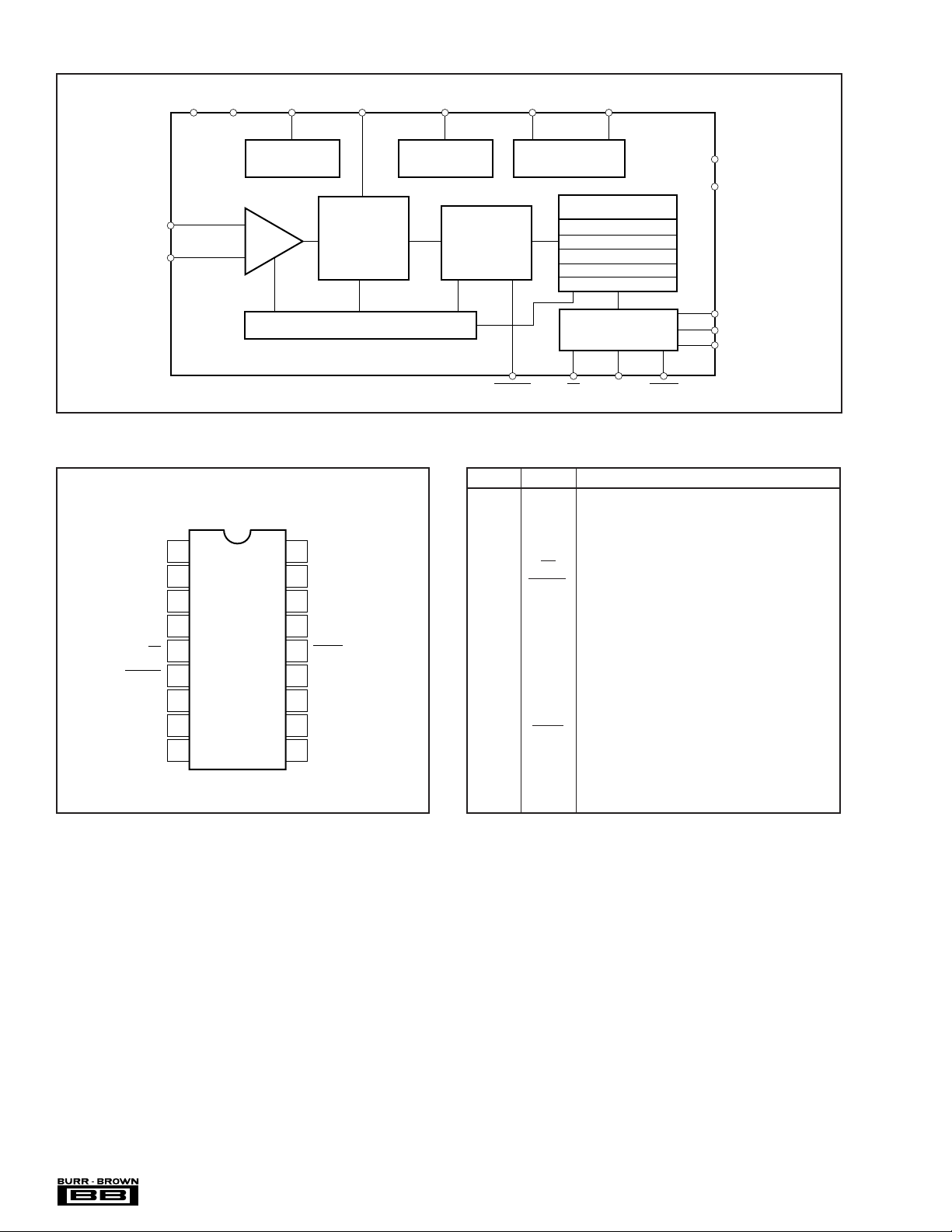
ADS1210 SIMPLIFIED BLOCK DIAGRAM
AGND AV
3
REF
DD
OUT
REF
IN
16 17 18 4 7 8
+2.5V
Reference
1
AINP
A
IN
2
N
PGA
Second-Order
∆Σ
Modulator
Modulator Control
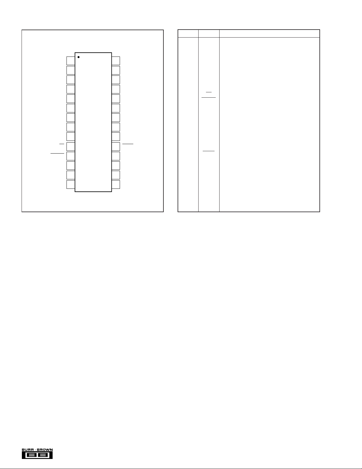
ADS1210 PIN CONFIGURATION
TOP VIEW DIP/SOIC
A
IN
A
IN
AGND
V
BIAS
CS
DSYNC
X
X
OUT
DGND
1
P
2
N
3
4
ADS1210
5
6
7
IN
8
9
18
17
16
15
14
13
12
11
10
REF
IN
REF
OUT
AV
DD
MODE
DRDY
SDOUT
SDIO
SCLK
DV
DD
V
BIAS
+3.3V Bias
Generator
X
IN
Clock Generator
Third-Order
Digital Filter
65 1415
DSYNC CS DRDYMODE
ADS1210 PIN DEFINITIONS
PIN NO NAME DESCRIPTION
1A
2A
3 AGND Analog Ground.
4V
5 CS Chip Select Input.
6 DSYNC Control Input to Synchronize Serial Output Data.
7X
8X
9 DGND Digital Ground.
10 DV
11 SCLK Clock Input/Output for serial data transfer.
12 SDIO Serial Data Input (can also function as Serial Data
13 SDOUT Serial Data Output.
14 DRDY Data Ready.
15 MODE SCLK Control Input (Master = 1, Slave = 0).
16 AV
17 REF
18 REF
P Noninverting Input.
IN
N Inverting Input.
IN
BIAS
IN
OUT
DD
DD
OUT
IN
X
OUT
9
DGND
DV
10
DD
Micro Controller
Instruction Register
Command Register
Data Output Register
Offset Register
Full-Scale Register
11
SCLK
Serial Interface
12
SDIO
13
SDOUT
Bias Voltage Output, +3.3V nominal.
System Clock Input.
System Clock Output (for Crystal or Resonator).
Digital Supply, +5V nominal.
Output).
Analog Supply, +5V nominal.
Reference Output, +2.5V nominal.
Reference Input.
®
ADS1210, 1211
4
ADS1211 SIMPLIFIED BLOCK DIAGRAM
AGND AV
REF
DD
OUT
REF
IN
6 19 20 21 7 10 11
+2.5V
4
1P
A
IN
5
A
1N
IN
2
A
2P
IN
3
A
2N
IN
A
3P
IN
A
3N
IN
A
4P
IN
A
4N
IN
MUX
24
1
22
23
Reference
PGA
Second-Order
∆∑
Modulator
Modulator Control
ADS1211P AND ADS1211U PIN CONFIGURATION
TOP VIEW DIP/SOIC
A
3N
IN
2P
A
IN
A
2N
IN
A
1P
IN
A
1N
IN
AGND
V
BIAS
CS
DSYNC
X
X
OUT
DGND
1
2
3
4
5
6
ADS1211P
7
ADS1211U
8
9
10
IN
11
12
24
23
22
21
20
19
18
17
16
15
14
13
3P
A
IN
4N
A
IN
A
4P
IN
REF
IN
REF
OUT
AV
DD
MODE
DRDY
SDOUT
SDIO
SCLK
DV
DD
V
BIAS
+3.3V Bias
Generator
X
IN
Clock Generator
X
OUT
12
13
Micro Controller
Third-Order
Digital Filter
Instruction Register
Command Register
Data Output Register
Offset Register
Full-Scale Register
14
Serial Interface
15
16
98 1718
DSYNC CS DRDYMODE
ADS1211P AND ADS1211U PIN DEFINITIONS
PIN NO NAME DESCRIPTION
1AIN3N Inverting Input Channel 3.
2AIN2P Noninverting Input Channel 2.
3A
4A
5AIN1N Inverting Input Channel 1.
6 AGND Analog Ground.
7V
8 CS Chip Select Input.
9 DSYNC Control Input to Synchronize Serial Output Data.
10 X
11 X
12 DGND Digital Ground.
13 DV
14 SCLK Clock Input/Output for serial data transfer.
15 SDIO Serial Data Input (can also function as Serial Data
16 SDOUT Serial Data Output.
17 DRDY Data Ready.
18 MODE SCLK Control Input (Master = 1, Slave = 0).
19 AV
20 REF
21 REF
22 A
23 AIN4N Inverting Input Channel 4.
24 A
2N Inverting Input Channel 2.
IN
1P Noninverting Input Channel 1.
IN
BIAS
OUT
Bias Voltage Output, +3.3V nominal.
System Clock Input.
IN
System Clock Output (for Crystal or Resonator).
Digital Supply, +5V nominal.
DD
Output).
Analog Supply, +5V nominal.
DD
Reference Output: +2.5V nominal.
OUT
Reference Input.
IN
4P Noninverting Input Channel 4.
IN
3P Noninverting Input Channel 3.
IN
DGND
DV
DD
SCLK
SDIO
SDOUT
5 ADS1210, 1211
®
ADS1211E PIN CONFIGURATION
TOP VIEW SSOP
A
3N
IN
A
2P
IN
A
2N
IN
A
1P
IN
A
1N
IN
AGND
V
BIAS
NIC
NIC
CS
DSYNC
X
X
OUT
DGND
1
2
3
4
5
6
7
ADS1211E
8
9
10
11
12
IN
13
14
28
27
26
25
24
23
22
21
20
19
18
17
16
15
3P
A
IN
A
4N
IN
A
4P
IN
REF
IN
REF
OUT
AV
DD
MODE
NIC
NIC
DRDY
SDOUT
SDIO
SCLK
DV
DD
ADS1211E PIN DEFINITIONS
PIN NO NAME DESCRIPTION
1A
2A
3AIN2N Inverting Input Channel 2.
4A
5A
6 AGND Analog Ground.
7V
8 NIC Not Internally Connected.
9 NIC Not Internally Connected.
10 CS Chip Select Input.
11 DSYNC Control Input to Synchronize Serial Output Data.
12 X
13 X
14 DGND Digital Ground.
15 DV
16 SCLK Clock Input/Output for serial data transfer.
17 SDIO Serial Data Input (can also function as Serial Data
18 SDOUT Serial Data Output.
19 DRDY Data Ready.
20 NIC Not Internally Connected.
21 NIC Not Internally Connected.
22 MODE SCLK Control Input (Master = 1, Slave = 0).
23 AV
24 REF
25 REF
26 A
27 AIN4N Inverting Input Channel 4.
28 A
3N Inverting Input Channel 3.
IN
2P Noninverting Input Channel 2.
IN
1P Noninverting Input Channel 1.
IN
1N Inverting Input Channel 1.
IN
BIAS
Bias Voltage Output, +3.3V nominal.
System Clock Input.
IN
System Clock Output (for Crystal or Resonator).
OUT
Digital Supply, +5V nominal.
DD
Output).
Analog Supply, +5V nominal.
DD
Reference Output: +2.5V nominal.
OUT
Reference Input.
IN
4P Noninverting Input Channel 4.
IN
3P Noninverting Input Channel 3.
IN
®
ADS1210, 1211
6
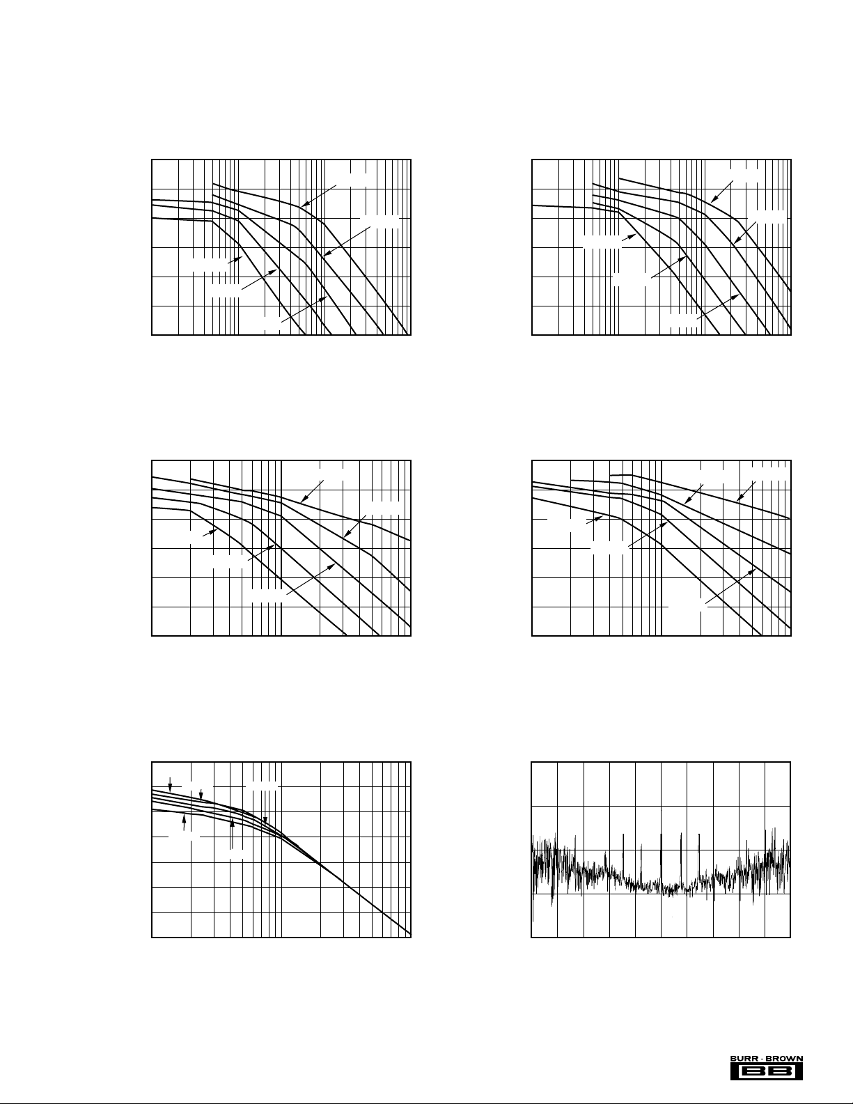
TYPICAL PERFORMANCE CURVES
At TA = +25°C, AVDD = DV
2.5V reference, unless otherwise noted.
DD =
+5V, f
= 10MHz, programmable gain amplifier setting of 1, Turbo Mode Rate of one, REF
XIN
disabled, V
OUT
disabled, and external
BIAS
EFFECTIVE RESOLUTION vs DATA RATE
24
22
20
18
16
14
Effective Resolution in Bits (rms)
12
24
22
20
18
16
14
Effective Resolution in Bits (rms)
12
10 100 1k
Turbo 1
Turbo 2
1 10 100 1k
EFFECTIVE RESOLUTION vs DATA RATE
Turbo 1
(1MHz Clock)
Turbo 16
Turbo 4
Data Rate (Hz)
(5MHz Clock)
Turbo 16
Turbo 2
Turbo 4
Data Rate (Hz)
Turbo 8
Turbo 8
EFFECTIVE RESOLUTION vs DATA RATE
24
22
20
18
16
14
Effective Resolution in Bits (rms)
12
1 10 100 1k
24
22
20
18
16
14
Effective Resolution in Bits (rms)
12
10 100 1k
Turbo 1
EFFECTIVE RESOLUTION vs DATA RATE
Turbo 1
(2.5MHz Clock)
Turbo 16
Turbo 2
Turbo 4
Data Rate (Hz)
(10MHz Clock)
Turbo 8
Turbo 2
Turbo 4
Data Rate (Hz)
Turbo 8
Turbo 16
24
22
20
18
16
14
12
Effective Resolution in Bits (rms)
10
EFFECTIVE RESOLUTION vs DATA RATE
PGA 1
PGA 2 PGA 4
PGA 16
PGA 8
10
Data Rate (Hz)
100 1k
RMS NOISE vs INPUT VOLTAGE LEVEL
2.5
2.0
1.5
RMS Noise (ppm)
1.0
0.5
–5.0 –4.0 –3.0 –2.0 –1.0 0 1.0 2.0 3.0 4.0 5.0
(60Hz Data Rate)
Analog Input Differential Voltage (V)
7 ADS1210, 1211
®
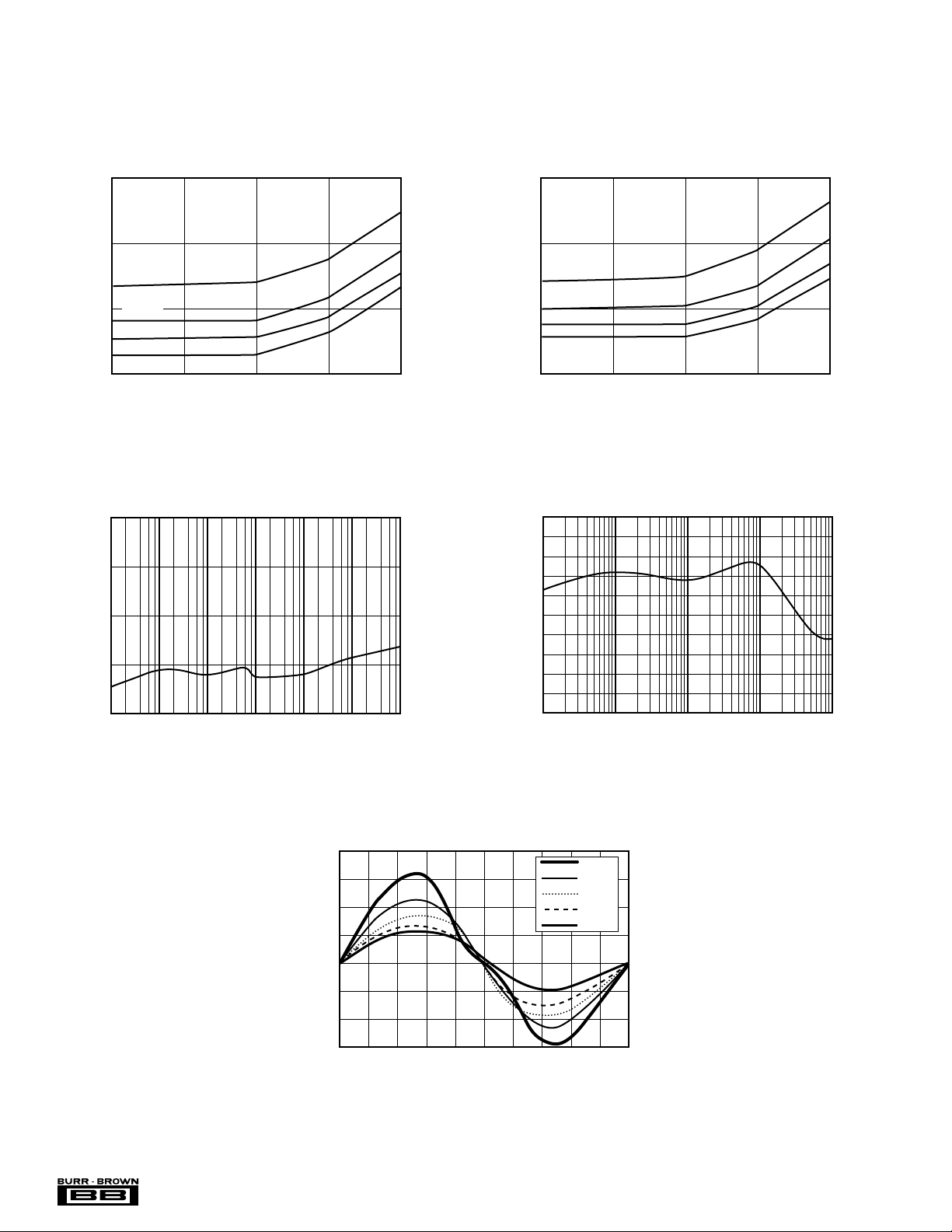
TYPICAL PERFORMANCE CURVES (CONT)
At TA = +25°C, AVDD = DV
2.5V reference, unless otherwise noted.
DD =
+5V, f
= 10MHz, programmable gain amplifier setting of 1, Turbo Mode Rate of 1, REF
XIN
disabled, V
OUT
disabled, and external
BIAS
POWER DISSIPATION vs TURBO MODE RATE
50.0
40.0
10MHz
30.0
Power Dissipation (mW)
20.0
85.0
80.0
5MHz
2.5MHz
1MHz
124816
(REF
Enabled)
OUT
Turbo Mode Rate
PSRR vs FREQUENCY
POWER DISSIPATION vs TURBO MODE RATE
40.0
30.0
10MHz
20.0
Power Dissipation (mW)
10.0
120.0
5MHz
2.5MHz
1MHz
124816
(External Reference; REF
Turbo Mode Rate
CMRR vs FREQUENCY
OUT
)
75.0
PSRR (dB)
70.0
65.0
0.1 1 10 100
Frequency (Hz)
115.0
CMRR (dB)
110.0
1k 10k 100k
LINEARITY vs TEMPERATURE
8
6
4
2
0
–2
Integral Nonlinearity (ppm)
–4
–6
–5 –4 –3 –2 –1 0 1 2 3 4 5
(60Hz Data Rate)
Analog Input Differential Voltage (V)
0.1 1 10
100 1k
Frequency (Hz)
–40°C
–5°C
+25°C
+55°C
+85°C
®
ADS1210, 1211
8

THEORY OF OPERATION
The ADS1210 and ADS1211 are precision, high dynamic
range, self-calibrating, 24-bit, delta-sigma A/D converters
capable of achieving very high resolution digital results.
Each contains a programmable gain amplifier (PGA); a
second-order delta-sigma modulator; a programmable digital filter; a microcontroller including the Instruction, Command and Calibration registers; a serial interface; a clock
generator circuit; and an internal 2.5V reference. The
ADS1211 includes a 4-channel input multiplexer.
In order to provide low system noise, common-mode rejection of 115dB and excellent power supply rejection, the
design topology is based on a fully differential switched
capacitor architecture. Turbo Mode, a unique feature of the
ADS1210/11, can be used to boost the sampling rate of the
input capacitor, which is normally 19.5kHz with a 10MHz
clock. By programming the Command Register, the sampling rate can be increased to 39kHz, 78kHz, 156kHz, or
312kHz. Each increase in sample rate results in an increase
in performance when maintaining the same output data rate.
The programmable gain amplifier (PGA) of the ADS1210/
11 can be set to a gain of 1, 2, 4, 8 or 16—substantially
increasing the dynamic range of the converter and simplifying the interface to the more common transducers (see Table
I). This gain is implemented by increasing the number of
samples taken by the input capacitor from 19.5kHz for a
gain of 1 to 312kHz for a gain of 16. Since the Turbo Mode
and PGA functions are both implemented by varying the
sampling frequency of the input capacitor, the combination
of PGA gain and Turbo Mode Rate is limited to 16 (see
Table II). For example, when using a Turbo Mode Rate of
8 (156kHz at 10MHz), the maximum PGA gain setting is 2.
ANALOG ANALOG INPUT
(1)
INPUT
FULL- EXAMPLE FULL- EXAMPLE
GAIN RANGE RANGE
SETTING (V) (V) (V) (V)
1 10 0 to 5 40 ±10
2 5 1.25 to 3.75 20 ±5
4 2.5 1.88 to 3.13 10 ±2.5
8 1.25 2.19 to 2.81 5 ±1.25
16 0.625 2.34 to 2.66 2.5 ±0.625
NOTE: (1) With a 2.5V reference, such as the internal reference. (2) This
example utilizes the circuit in Figure 12. Other input ranges are possible. (3)
The ADS1210/11 allows common-mode voltage as long as the absolute
input voltage on A
SCALE VOLTAGE SCALE VOLTAGE
P or AINN does not go below AGND or above AVDD.
IN
UTILIZING V
(3)
RANGE RANGE
BIAS
(1,2)
(3)
TABLE I. Full-Scale Range vs PGA Setting.
TURBO MODE RATE AVAILABLE PGA SETTINGS
1 1, 2, 4, 8, 16
2 1, 2, 4, 8
4 1, 2, 4
8 1, 2
16 1
The output data rate of the ADS1210/11 can be varied from
a few hertz to as much as 15,625kHz, trading off lower
resolution results for higher data rates. In addition, the data
rate determines the first null of the digital filter and sets the
–3dB point of the input bandwidth (see the Digital Filter
section). Changing the data rate of the ADS1210/11 does not
result in a change in the sampling rate of the input capacitor.
The data rate effectively sets the number of samples which
are used by the digital filter to obtain each conversion result.
A lower data rate results in higher resolution, lower input
bandwidth, and different notch frequencies than a higher
data rate. It does not result in any change in input impedance
or modulator frequency, or any appreciable change in power
consumption.
The ADS1210/11 also includes complete on-board calibration that can correct for internal offset and gain errors or
limited external system errors. Internal calibration can be
run when needed, or automatically and continuously in the
background. System calibration can be run as needed and the
appropriate input voltages must be provided to the ADS1210/
11. For this reason, there is no continuous System Calibration Mode. The calibration registers are fully readable and
writable. This feature allows for switching between various
configurations—different data rates, Turbo Mode Rates, and
gain settings—without re-calibrating.
The various settings, rates, modes, and registers of the
ADS1210/11 are read or written via a synchronous serial
interface. This interface can operate in either a self-clocked
mode (Master Mode) or an externally clocked mode (Slave
Mode). In the Master Mode, the serial clock (SCLK) frequency is one-half of the ADS1210/11 XIN clock frequency.
This is an important consideration for many systems and
may determine the maximum ADS1210/11 clock that can be
used.
The high resolution and flexibility of the ADS1210/11 allow
these converters to fill a wide variety of A/D conversion
tasks. In order to ensure that a particular configuration will
meet the design goals, there are several important items
which must be considered. These include (but are certainly
not limited to) the needed resolution, required linearity,
desired input bandwidth, power consumption goal, and sensor output voltage.
The remainder of this data sheet discusses the operation of
the ADS1210/11 in detail. In order to allow for easier
comparison of different configurations, “effective resolution” is used as the figure of merit for most tables and
graphs. For example, Table III shows a comparison between
data rate (and –3dB input bandwidth) versus PGA setting at
a Turbo Mode Rate of 1 and a clock rate of 10MHz. See the
Definition of Terms section for a definition of effective
resolution.
TABLE II. Available PGA Settings vs Turbo Mode Rate.
®
9 ADS1210, 1211

DATA -3DB
RATE FREQUENCY
(HZ) (HZ) G = 1 G = 2 G = 4 G = 8 G = 16
10 2.62 21.5 21.0 21.0 21.0 20.0
25 6.55 20.5 20.5 20.5 20.0 19.5
30 7.86 20.5 20.5 20.5 20.0 19.5
50 13.1 20.0 20.0 20.0 19.5 19.0
60 15.7 19.5 19.5 19.5 19.0 19.0
100 26.2 18.0 18.0 18.0 18.0 18.0
250 65.5 15.0 15.0 15.0 15.0 15.0
500 131 12.5 12.5 12.5 12.5 12.5
1000 262 10.0 10.5 10.0 10.0 10.0
EFFECTIVE RESOLUTION (BITS RMS)
TABLE III. Effective Resolution vs Data Rate and Gain
Setting. (Turbo Mode Rate of 1 and a 10MHz
clock.)
DEFINITION OF TERMS
An attempt has been made to be consistent with the terminology used in this data sheet. In that regard, the definition
of each term is given as follows:
Analog Input Differential Voltage—For an analog signal
that is fully differential, the voltage range can be compared
to that of an instrumentation amplifier. For example, if both
analog inputs of the ADS1210 are at 2.5V, then the differential voltage is 0V. If one is at 0V and the other at 5V, then
the differential voltage magnitude is 5V. But, this is the case
regardless of which input is at 0V and which is at 5V, while
the digital output result is quite different.
The analog input differential voltage is given by the following equation: AINP – AINN. Thus, a positive digital output is
produced whenever the analog input differential voltage is
positive, while a negative digital output is produced whenever the differential is negative.
For example, when the converter is configured with a 2.5V
reference and placed in a gain setting of 2, the positive fullscale output is produced when the analog input differential
is 2.5V. The negative full-scale output is produced when the
differential is –2.5V. In each case, the actual input voltages
must remain within the AGND to AVDD range (see Table I).
Actual Analog Input Voltage—The voltage at any one
analog input relative to AGND.
Full-Scale Range (FSR)—As with most A/D converters,
the full-scale range of the ADS1210/11 is defined as the
“input” which produces the positive full-scale digital output
minus the “input” which produces the negative full-scale
digital output.
For example, when the converter is configured with a 2.5V
reference and is placed in a gain setting of 2, the full-scale
range is: [2.5V (positive full scale) minus –2.5V (negative
full scale)] = 5V.
Typical Analog Input Voltage Range—This term describes the actual voltage range of the analog inputs which
will cover the converter’s full-scale range, assuming that
each input has a common-mode voltage that is greater than
REFIN/PGA and smaller than (AVDD – REFIN/PGA).
For example, when the converter is configured with a 2.5V
reference and placed in a gain setting of 2, the typical input
voltage range is 1.25V to 3.75V. However, an input range of
0V to 2.5V or 2.5V to 5V would also cover the converter’s
full-scale range.
Voltage Span—This is simply the magnitude of the typical
analog input voltage range. For example, when the converter
is configured with a 2.5V reference and placed in a gain
setting of 2, the input voltage span is 2.5V.
Least Significant Bit (LSB) Weight—This is the theoretical amount of voltage that the differential voltage at the
analog input would have to change in order to observe a
change in the output data of one least significant bit. It is
computed as follows:
LSB Weight =
Full−Scale Range
N
2
where N is the number of bits in the digital output.
Effective Resolution—The effective resolution of the
ADS1210/11 in a particular configuration can be expressed
in two different units: bits rms (referenced to output) and
microvolts rms (referenced to input). Computed directly
from the converter’s output data, each is a statistical calculation based on a given number of results. Knowing one, the
other can be computed as follows:
10V
ER in bits rms =
ER in Vrms =
20• log
PGA
ER in Vrms
6.02
10V
PGA
6.02•ER in bits rms +1.76
10
20
−1.76
The 10V figure in each calculation represents the full-scale
range of the ADS1210/11 in a gain setting of 1. This means
that both units are absolute expressions of resolution—the
performance in different configurations can be directly compared regardless of the units. Comparing the resolution of
different gain settings expressed in bits rms requires accounting for the PGA setting.
Main Controller—A generic term for the external
microcontroller, microprocessor, or digital signal processor
which is controlling the operation of the ADS1210/11 and
receiving the output data.
®
ADS1210, 1211
10
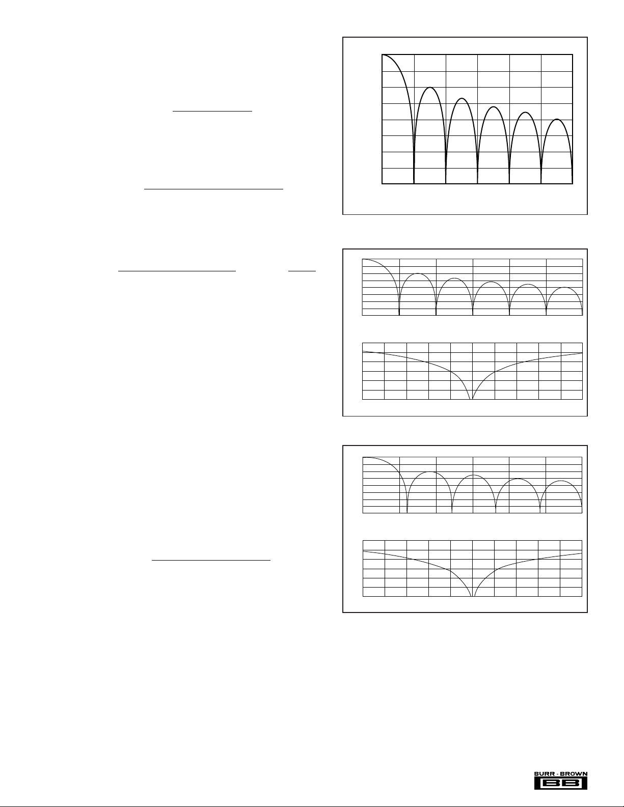
f
FILTER RESPONSE
Frequency (Hz)
–40
–60
–80
–100
–120
–140
–160
55 56 57 58 59 60 61 62 63 64 65
FILTER RESPONSE
Frequency (Hz)
0
–20
–40
–60
–80
–100
–120
–140
–160
0 50 100 150 200 250 300
Gain (dB) Gain (dB)
—The frequency of the crystal oscillator or CMOS
XIN
compatible input signal at the XIN input of the ADS1210/11.
f
—The frequency or speed at which the modulator of the
MOD
ADS1210/11 is running, given by the following equation:
•Turbo Mode
f
f
MOD
f
—The frequency or switching speed of the input
SAMP
XIN
=
512
sampling capacitor. The value is given by the following
equation:
•Turbo Mode• Gain Setting
f
XIN
=
512
—The frequency of the digital output data
f
DATA
, t
f
SAMP
DATA
produced by the ADS1210/11 or the inverse of this (the
period), respectively, f
f
f
DATA
=
XIN
512• DecimationRatio +1
()
is also referred to as the data rate.
DATA
•Turbo Mode
,t
DATA
1
=
f
DATA
Conversion Cycle—The term “conversion cycle” usually
refers to a discrete A/D conversion operation, such as that
performed by a successive approximation converter. As
used here, a conversion cycle refers to the t
time period.
DATA
However, each digital output is actually based on the modulator results from the last three t
time periods.
DATA
DIGITAL FILTER
The digital filter of the ADS1210/11 computes the output
result based on the most recent results from the delta-sigma
modulator. The number of modulator results that are used
depend on the decimation ratio set in the Command Register. At the most basic level, the digital filter can be thought
of as simply averaging the modulator results and presenting
this average as the digital output.
While the decimation ratio determines the number of modulator results to use, the modulator runs faster at higher Turbo
Modes. These two items, together with the ADS1210/11
clock frequency, determine the output data rate:
0
–20
–40
–60
–80
Gain (dB)
–100
–120
–140
–160
NORMALIZED DIGITAL FILTER RESPONSE
0123456
Frequency (Hz)
FIGURE 1. Normalized Digital Filter Response.
0
–20
–40
–60
–80
–100
Gain (dB)
–120
–140
–160
0 50 100 150 200 250 300
–40
–60
–80
–100
Gain (dB)
–120
–140
–160
45 46 47 48 49 50 51 52 53 54 55
FILTER RESPONSE
Frequency (Hz)
FILTER RESPONSE
Frequency (Hz)
FIGURE 2. Digital Filter Response at a Data Rate of 50Hz.
•Turbo Mode
f
f
DATA
=
XIN
512• Decimation Ratio +1
()
Also, since the conversion result is essentially an average,
the data rate determines where the resulting notches are in
the digital filter. For example, if the output data rate is 1kHz,
then a 1kHz input frequency will average to zero during the
1ms conversion cycle. Likewise, a 2kHz input frequency
will average to zero, etc.
In this manner, the data rate can be used to set specific notch
frequencies in the digital filter response (see Figure 1 for the
normalized response of the digital filter). For example, if the
rejection of power line frequencies is desired, then the data
rate can simply be set to the power line frequency. Figures
2 and 3 show the digital filter response for a data rate of
50Hz and 60Hz, respectively.
FIGURE 3. Digital Filter Response at a Data Rate of 60Hz.
If the effective resolution at a 50Hz or 60Hz data rate is not
adequate for the particular application, then power line frequencies could still be rejected by operating the ADS1210/11
at 25/30Hz, 16.7/20Hz, 12.5/15Hz, etc. If a higher data rate
is needed, then power line frequencies must either be rejected
before conversion (with an analog notch filter) or after
conversion (with a digital notch filter running on the main
controller).
®
11 ADS1210, 1211
Filter Equation
The digital filter is described by the following transfer
function:
3
|H(f)|=
sin
N •sin
π•f • N
f
MOD
π•f
f
MOD
where N is the Decimation Ratio.
This filter has a (sin(x)/x)3 response and is referred to a sinc
filter. For the ADS1210/11, this type of filter allows the data
rate to be changed over a very wide range (nearly four orders
of magnitude). However, the –3dB point of the filter is 0.262
times the data rate. And, as can be seen in Figures 1 and 2,
the rejection in the stopband (frequencies higher than the
first notch frequency) may only be –40dB.
These factors must be considered in the overall system
design. For example, with a 50Hz data rate, a significant
signal at 75Hz may alias back into the passband at 25Hz.
The analog front end can be designed to provide the needed
attenuation to prevent aliasing, or the system may simply
provide this inherently. Another possibility is increasing the
data rate and then post filtering with a digital filter on the
main controller.
Filter Settling
The number of modulator results used to compute each
conversion result is three times the Decimation Ratio. This
means that any step change (or any channel change for the
ADS1211) will require at least three conversions to fully
settle. However, if the change occurs asynchronously, then at
least four conversions are required to ensure complete settling. For example, on the ADS1211, the fourth conversion
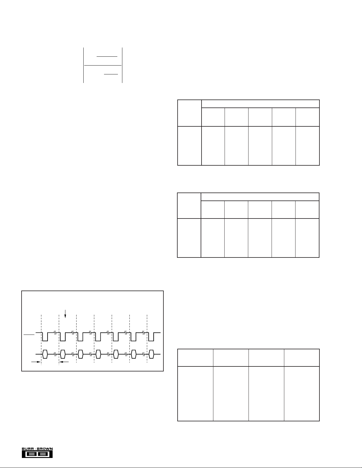
result after a channel change will be valid (see Figure 4).
Significant Analog Input Change
ADS1211 Channel Change
Valid
Data
DRDY
or
Valid
Data
Data
not
Valid
Data
not
Valid
Data
not
Valid
Valid
Data
Valid
Data
the effective resolution of the output data at a given data rate,
but there is also an increase in power dissipation. For Turbo
Mode Rates 2 and 4, the increase is slight. For rates 8 and
16, the increase is more substantial. See the Typical Performance Curves for more information.
In a Turbo Mode Rate of 16, the ADS1210/11 can offer 20
bits of effective resolution at a 1kHz data rate. A comparison
of effective resolution versus Turbo Mode Rates and output
data rates is shown in Table IV while Table V shows the
corresponding noise level in µVrms.
3
Data Turbo Turbo Turbo Turbo Turbo
Rate Mode Mode Mode Mode Mode
(Hz) Rate 1 Rate 2 Rate 4 Rate 8 Rate 16
10 21.5 22.0 22.5
20 21.0 22.0 22.0 22.5
40 20.0 21.5 22.0 22.5 23.0
50 20.0 21.5 21.5 22.0 23.0
60 19.5 21.0 21.5 22.0 23.0
100 18.0 20.0 21.0 21.5 22.5
1000 10.0 12.5 15.0 17.5 20.0
Effective Resolution (Bits rms)
TABLE IV. Effective Resolution vs Data Rate and Turbo Mode
Rate. (Gain setting of 1 and 10MHz clock.)
NOISE LEVEL (µVrms)
DATA TURBO TURBO TURBO TURBO TURBO
RATE MODE MODE MODE MODE MODE
(Hz) RATE 1 RATE 2 RATE 4 RATE 8 RATE 16
10 2.9 1.7 1.3
20 4.3 2.1 1.7 1.3
40 6.9 3.0 2.3 1.6 1.0
50 8.1 3.2 2.4 1.8 1.0
60 10.5 3.9 2.6 1.9 1.0
100 26.9 6.9 3.5 2.7 1.4
1000 6909.7 1354.5 238.4 46.6 7.8
TABLE V. Noise Level vs Data Rate and Turbo Mode Rate.
(Gain setting of 1 and 10MHz clock.)
The Turbo Mode feature allows trade-offs to be made
between the ADS1210/11 XIN clock frequency, power dissipation, and effective resolution. If a 5MHz clock is available
but a 10MHz clock is needed to achieve the desired performance, a Turbo Mode Rate of 2X will result in the same
effective resolution. Table VI provides a comparison of
effective resolution at various clock frequencies, data rates,
and Turbo Mode Rates.
Serial
I/O
t
DATA
FIGURE 4. Asynchronous ADS1210/11 Analog Input Volt-
age Step or ADS1211 Channel Change to Fully
Settled Output Data.
TURBO MODE
The ADS1210/11 offers a unique Turbo Mode feature which
can be used to increase the modulator sampling rate by 2, 4,
8, or 16 times normal. With the increase of modulator
sampling frequency, there can be a substantial increase in
®
ADS1210, 1211
DATA XIN CLOCK TURBO EFFECTIVE
RATE FREQUENCY MODE RESOLUTION
(Hz) (MHz) RATE (Bits rms)
60 10 1 19.5
60 5 2 19.5
60 2.5 4 19.5
60 1.25 8 19.5
60 0.625 16 19.5
100 10 1 18.0
100 5 2 18.0
100 2.5 4 18.0
100 1.25 8 18.0
100 0.625 16 18.0
TABLE VI. Effective Resolution vs Data Rate, Clock
Frequency, and Turbo Mode Rate. (Gain setting of 1.)
12

The Turbo Mode Rate (TMR) is programmed via the Sampling Frequency bits of the Command Register. Due to the
increase in input capacitor sampling frequency, higher Turbo
Mode settings result in lower analog input impedance;
AIN Impedance (Ω) = (10MHz/f
)•4.3E6/(G•TMR)
XIN
where G is the gain setting. Because the modulator rate also
changes in direct relation to the Turbo Mode setting, higher
values result in a lower impedance for the REFIN input:
REFIN Impedance (Ω) = (10MHz/f
)•1E6/TMR
XIN
The Turbo Mode Rate can be set to 1, 2, 4, 8, or 16. Consult
the graphs shown in the Typical Performance Curves for full
details on the performance of the ADS1210/11 operating in
different Turbo Mode Rates. Keep in mind that higher Turbo
Mode Rates result in fewer available gain settings as shown
in Table II.
PROGRAMMABLE GAIN AMPLIFIER
The programmable gain amplifier gain setting is programmed
via the PGA Gain bits of the Command Register. Changes
in the gain setting (G) of the programmable gain amplifier
results in an increase in the input capacitor sampling frequency. Thus, higher gain settings result in a lower analog
input impedance:
AIN Impedance (Ω) = (10MHz/f
)•4.3E6/(G•TMR)
XIN
where TMR is the Turbo Mode Rate. Because the modulator
speed does not depend on the gain setting, the input impedance seen at REFIN does not change.
The PGA can be set to gains of 1, 2, 4, 8, or 16. These gain
settings with their resulting full-scale range and typical
voltage range are shown in Table I. Keep in mind that higher
Turbo Mode Rates result in fewer available gain settings as
shown in Table II.
SOFTWARE GAIN
The excellent performance, flexibility, and low cost of the
ADS1210/11 allow the converter to be considered for designs which would not normally need a 24-bit ADC. For
example, many designs utilize a 12-bit converter and a highgain INA or PGA for digitizing low amplitude signals. For
some of these cases, the ADS1210/11 by itself may be a
solution, even though the maximum gain is limited to 16.
To get around the gain limitation, the digital result can
simply be shifted up by “n” bits in the main controller—
resulting in a gain of “n” times G, where G is the gain
setting. While this type of manipulation of the output data
is obvious, it is easy to miss how much the gain can be
increased in this manner on a 24-bit converter.
For example, shifting the result up by three bits when the
ADS1210/11 is set to a gain of 16 results in an effective gain
of 128. At lower data rates, the converter can easily provide
more than 12 bits of resolution. Even higher gains are
possible. The limitation is a combination of the needed data
rate, desired noise performance, and desired linearity.
CALIBRATION
The ADS1210/11 offers several different types of calibration, and the particular calibration desired is programmed
via the Command Register. In the case of Background
Calibration, the calibration will repeat at regular intervals
indefinitely. For all others, the calibration is performed once
and then normal operation is resumed.
Each type of calibration is covered in detail in their respective section. In general, calibration is recommended immediately after power-on and whenever there is a “significant”
change in the operating environment. The amount of change
which should cause a re-calibration is dependent on the
application, effective resolution, etc. Where high accuracy is
important, re-calibration should be done on changes in
temperature and power supply. In all cases, re-calibration
should be done when the gain, Turbo Mode, or data rate is
changed.
After a calibration has been accomplished, the Offset Calibration Register and the Full-Scale Calibration Register
contain the results of the calibration. The data in these
registers are accurate to the effective resolution of the
ADS1210/11’s mode of operation during the calibration.
Thus, these values will show a variation (or noise) equivalent to a regular conversion result.
For those cases where this error must be reduced, it is
tempting to consider running the calibration at a slower data
rate and then increasing the converter’s data rate after the
calibration is complete. Unfortunately, this will not work as
expected. The reason is that the results calculated at the
slower data rate would not be valid for the higher data rate.
Instead, the calibration should be done repeatedly. After
each calibration, the results can be read and stored. After the
desired number of calibrations, the main controller can
compute an average and write this value into the calibration
registers. The resulting error in the calibration values will be
reduced by the square root of the number of calibrations
which were averaged.
The calibration registers can also be used to provide system
offset and gain corrections separate from those computed by
the ADS1210/11. For example, these might be burned into
E2PROM during final product testing. On power-on, the
main controller would load these values into the calibration
registers. A further possibility is a look-up table based on the
current temperature.
Note that the values in the calibration registers will vary from
configuration to configuration and from part to part. There is
no method of reliably computing what a particular calibration
register should be to correct for a given amount of system
error. It is possible to present the ADS1210/11 with a known
amount of error, perform a calibration, read the desired
calibration register, change the error value, perform another
calibration, read the new value and use these values to
interpolate an intermediate value.
13 ADS1210, 1211
®

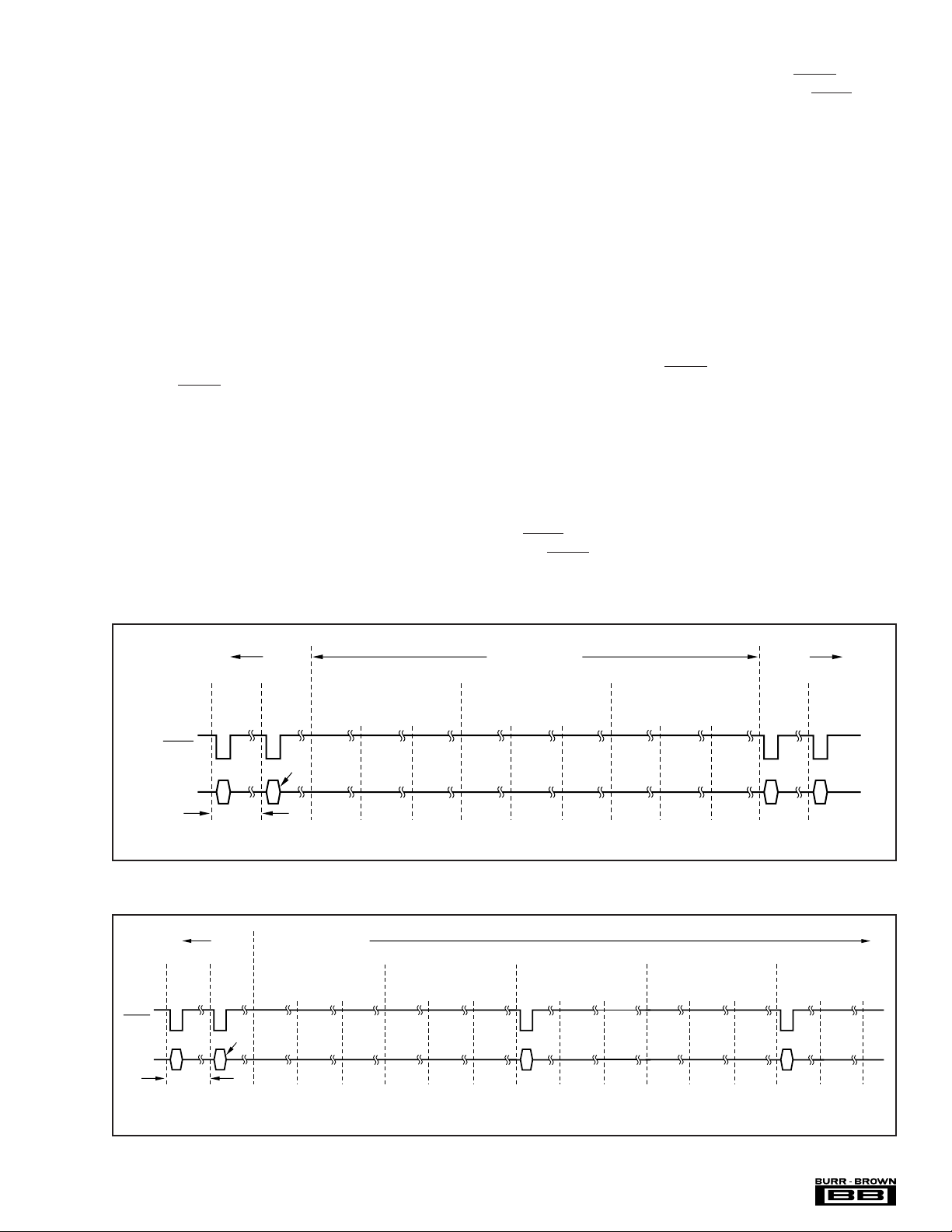
Normal
Mode
Valid
Data
DRDY
Serial
I/O
t
DATA
Valid
Data
SC
(1)
NOTES: (1) SC = Self-Calibration instruction. (2) In Slave Mode, this function requires 4 cycles.
FIGURE 5. Self-Calibration Timing.
Offset
Calibration on
Internal Offset
Self-Calibration
Mode
Full-Scale
(2)
Calibration on
Internal Full-Scale
Analog
Input
Conversion
Normal
Mode
Valid
Data
Valid
Data
Self-Calibration
A self-calibration is performed after the bits 001 have been
written to the Command Register Operation Mode bits
(MD2 through MD0). This initiates the following sequence
at the start of the next conversion cycle (see Figure 5). The
DRDY signal will not go LOW but will remain HIGH and
will continue to remain HIGH throughout the calibration
sequence. The inputs to the sampling capacitor are disconnected from the converter’s analog inputs and are shorted
together. An offset calibration is performed over the next
three conversion periods (four in Slave Mode). Then, the
input to the sampling capacitor is connected across REFIN,
and a full-scale calibration is performed over the next three
conversions.
After this, the Operation Mode bits are reset to 000 (normal
mode) and the input capacitor is reconnected to the input.
Conversions proceed as usual over the next three cycles in
order to fill the digital filter. DRDY remains HIGH during
this time. On the start of the fourth cycle, DRDY goes LOW
indicating valid data and resumption of normal operation.
System Offset Calibration
A system offset calibration is performed after the bits 010
have been written to the Command Register Operation
Mode bits (MD2 through MD0). This initiates the following
sequence (see Figure 6). At the start of the next conversion
cycle, the DRDY signal will not go LOW but will remain
HIGH and will continue to remain HIGH throughout the
calibration sequence. The offset calibration will be performed on the differential input voltage present at the
converter’s input over the next three conversion periods
(four in Slave Mode). When this is done, the Operation
Mode bits are reset to 000 (Normal Mode). A single conversion is done with DRDY HIGH. After this conversion, the
DRDY signal goes LOW indicating resumption of normal
operation.
Normal operation returns within a single conversion cycle
because it is assumed that the input voltage at the converter’s
input is not removed immediately after the offset calibration
is performed. In this case, the digital filter already contains
a valid result.
For full system calibration, offset calibration must be performed first and then full-scale calibration. In addition, the
offset calibration error will be the rms sum of the conversion
error and the noise on the system offset voltage. See the
System Calibration Limits section for information regarding
the limits on the magnitude of the system offset voltage.
System Full-Scale Calibration
A system full-scale calibration is performed after the bits
011 have been written to the Command Register Operation
Mode bits (MD2 through MD0). This initiates the following
sequence (see Figure 7). At the start of the next conversion
cycle, the DRDY signal will not go LOW but will remain
HIGH and will continue to remain HIGH throughout the
calibration sequence. The full-scale calibration will be performed on the differential input voltage (2 • REFIN/G)
present at the converter’s input over the next three conversion periods (four in Slave Mode). When this is done, the
Operation Mode bits are reset to 000 (Normal Mode). A
single conversion is done with DRDY HIGH. After this
conversion, the DRDY signal goes LOW indicating resumption of normal operation.
DRDY
Serial
I/O
Valid
Data
t
DATA
Normal
Mode
Valid
Data
(1)
SOC
NOTES: (1) SOC = System Offset Calibration instruction.
(2) In Slave Mode, this function requires 4 cycles.
System Offset
Calibration Mode
Offset
Calibration on
System Offset
Analog
Input
(2)
Conversion
FIGURE 6. System Offset Calibration Timing.
®
ADS1210, 1211
Normal
Mode
Possibly
Valid
Data
Possibly
Valid
Data
DRDY
Serial
I/O
Normal
Mode
Valid
Valid
Data
Data
(1)
SFSC
t
DATA
NOTES: (1) SFSC = System Full-Scale Calibration instruction.
(2) In Slave Mode, this function requires 4 cycles.
System Full-Scale
Calibration Mode
Full-Scale
Calibration on
System Full-Scale
(2)
Analog
Input
Conversion
FIGURE 7. System Full-Scale Calibration Timing.
14
Normal
Mode
Possibly
Valid
Data
Possibly
Valid
Data
Normal operation returns within a single conversion cycle
because it is assumed that the input voltage at the converter’s
input is not removed immediately after the full-scale calibration is performed. In this case, the digital filter already
contains a valid result.
For full system calibration, offset calibration must be performed first and then full-scale calibration. The calibration
error will be a sum of the rms noise on the conversion result
and the input signal noise. See the System Calibration Limits
section for information regarding the limits on the magnitude of the system full-scale voltage.
Pseudo System Calibration
The Pseudo System Calibration is performed after the bits
100 have been written to the Command Register Operation
Mode bits (MD2 through MD0). This initiates the following
sequence (see Figure 8). At the start of the next conversion
cycle, the DRDY signal will not go LOW but will remain
HIGH and will continue to remain HIGH throughout the
calibration sequence. The offset calibration will be performed
on the differential input voltage present at the converter’s
input over the next three conversion periods (four in Slave
Mode). Then, the input to the sampling capacitor is disconnected from the converter’s analog input and connected
across REFIN. A gain calibration is performed over the next
three conversions.
After this, the Operation Mode bits are reset to 000 (normal
mode) and the input capacitor is then reconnected to the
input. Conversions proceed as usual over the next three
cycles in order to fill the digital filter. DRDY remains
HIGH during this time. On the next cycle, the DRDY signal
goes LOW indicating valid data and resumption of normal
operation.
The system offset calibration range of the ADS1210/11
is limited and is listed in the Specifications Table. For
more information on how to use these specifications, see
the System Calibration Limits section. To calculate VOS,
use 2 • REFIN/ GAIN for VFS.
Background Calibration
The Background Calibration Mode is entered after the bits
101 have been written to the Command Register Operation
Mode bits (MD2 through MD0). This initiates the following
continuous sequence (see Figure 9). At the start of the next
conversion cycle, the DRDY signal will not go LOW but
will remain HIGH. The inputs to the sampling capacitor are
disconnected from the converter’s analog input and shorted
together. An offset calibration is performed over the next
three conversion periods (in Slave Mode, the very first offset
calibration requires four periods and all subsequent offset
calibrations require three periods). Then, the input capacitor
is reconnected to the input. Conversions proceed as usual
over the next three cycles in order to fill the digital filter.
DRDY remains HIGH during this time. On the next cycle,
the DRDY signal goes LOW indicating valid data.
Normal
Mode
Offset
Calibration on
System Offset
DRDY
Serial
I/O
Valid
Data
t
DATA
Valid
Data
(1)
PSC
NOTES: (1) PSC = Pseudo System Calibration instruction. (2) In Slave Mode, this function requires 4 cycles.
FIGURE 8. Pseudo System Calibration Timing.
DRDY
Serial
I/O
Valid
Data
t
DATA
Normal
Background Calibration
Mode
Mode
Valid
Data
(1)
BC
Offset
Calibration on
Internal Offset
(2)
NOTES: (1) BC = Background Calibration instruction. (2) In Slave Mode, the very first offset
calibration will require 4 cycles. All subsequent offset calibrations will require 3 cycles.
(2)
Analog
Input
Conversion
Pseudo System
Calibration Mode
Full-Scale
Calibration on
Internal Full-Scale
Full-Scale
Calibration on
Internal Full-Scale
Analog
Input
Conversion
Analog
Conversion
Input
Normal
Mode
Valid
Data
Valid
Data
Cycle Repeats
with Offset
Calibration
FIGURE 9. Background Calibration Timing.
®
15 ADS1210, 1211

Also, during this cycle, the sampling capacitor is disconnected from the converter’s analog input and is connected
across REFIN. A gain calibration is initiated and proceeds
over the next three conversions. After this, the input capacitor is once again connected to the analog input. Conversions
proceed as usual over the next three cycles in order to fill the
digital filter. DRDY remains HIGH during this time. On the
next cycle, the DRDY signal goes LOW indicating valid
data, the input to the sampling capacitor is shorted, and an
offset calibration is initiated. At this point, the Background
Calibration sequence repeats.
In essence, the Background Calibration Mode performs
continuous self-calibration where the offset and gain calibrations are interleaved with regular conversions. Thus, the
data rate is reduced by a factor of 6. The advantage is that
the converter is continuously adjusting to environmental
changes such as ambient or component temperature (due to
airflow variations).
The ADS1210/11 will remain in the Background Calibration Mode indefinitely. To move to any other mode, the
Command Register Operation Mode bits (MD2 through
MD0) must be set to the appropriate values.
System Calibration Offset and Full-Scale
Calibration Limits
The System Offset and Full-Scale Calibration range of the
ADS1210/11 is limited and is listed in the Specifications
Table. The range is specified as:
(VFS – | V
(VFS – | V
where VFS is the system full-scale voltage and | V
|) < 1.3 • (2 • REFIN)/GAIN
OS
|) > 0.7 • (2 • REFIN)/GAIN
OS
OS
| is the
absolute value of the system offset voltage. In the following
discussion, keep in mind that these voltages are differential
voltages.
For example, with the internal reference (2.5V) and a gain of
two, the previous equations become (after some manipulation):
VFS – 3.25 < VOS < VFS – 1.75
If VFS is perfect at 2.5V (positive full-scale), then VOS must
be greater than –0.75V and less than 0.75V. Thus, when offset
calibration is performed, the positive input can be no more
than 0.75V below or above the negative input. If this range is
exceeded, the ADS1210/11 may not calibrate properly.
This calculation method works for all gains other than one.
For a gain of one and the internal reference (2.5V), the
equation becomes:
VFS – 6.5 < VOS < VFS – 3.5
With a 5V positive full-scale input, VOS must be greater than
–1.5V and less than 1.5V. Since the offset represents a
common-mode voltage and the input voltage range in a gain
of one is 0V to 5V, a common-mode voltage will cause the
actual input voltage to possibly go below 0V or above 5V.
The specifications also show that for the specifications to be
valid, the input voltage must not go below AGND by more
than 30mV or above AVDD by more than 30mV.
This will be an important consideration in many systems
which use a 2.5V or greater reference, as the input range is
constrained by the expected power supply variations. In
addition, the expected full-scale voltage will impact the
allowable offset voltage (and vice-versa) as the combination
of the two must remain within the power supply and ground
potentials, regardless of the results obtained via the range
calculation shown previously.
There are only two solutions to this constraint: either the
system design must ensure that the full-scale and offset
voltage variations will remain within the power supply and
ground potentials, or the part must be used in a gain of 2 or
greater.
SLEEP MODE
The Sleep Mode is entered after the bits 110 have been
written to the Command Register Operation Mode bits
(MD2 through MD0). This mode is exited by entering a new
mode into the MD2-MD0 bits.
The Sleep Mode causes the analog section and a good deal
of the digital section to power down. For full analog power
down, the V
generator and the internal reference must
BIAS
also be powered down by setting the BIAS and REFO bits
in the Command Register accordingly. The power dissipation shown in the Specifications Table is with the internal
reference and the V
generator disabled.
BIAS
To initiate serial communication with the converter while it
is in Sleep Mode, one of the following procedures must be
used: If CS is being used, simply taking CS LOW will
enable serial communication to proceed normally. If CS is
not being used (tied LOW) and the ADS1210/11 is in the
Master Mode, then a falling edge must be produced on the
SDIO line. If SDIO is LOW, the SDIO line must be taken
HIGH for 2 • t
periods (minimum) and then taken LOW.
XIN
Alternatively, SDIO can be forced HIGH after putting the
ADS1210/11 to “sleep” and then taken LOW when the
Sleep Mode is to be exited. Finally, if CS is not being used
(tied LOW) and the ADS1210/11 is in the Slave Mode, then
simply sending a normal Instruction Register command will
re-establish communication.
Once serial communication is resumed, the Sleep Mode is
exited by changing the MD2-MD0 bits to any other mode.
When a new mode (other than Sleep) has been entered, the
ADS1210/11 will execute a very brief internal power-up
sequence of the analog and digital circuitry. Once this has
been done, one normal conversion cycle is performed before
the new mode is actually entered. At the end of this conversion
cycle, the new mode takes effect and the converter will
respond accordingly. The DRDY signal will remain HIGH
through the first conversion cycle. It will also remain HIGH
through the second, even if the new mode is the Normal Mode.
If the V
generator and/or the internal reference have
BIAS
been disabled, then they must be manually re-enabled via the
appropriate bits in the Command Register. In addition, the
internal reference will have to charge the external bypass
capacitor(s) and possibly other circuitry. There may also be
®
ADS1210, 1211
16

considerations associated with V
and the settling of
BIAS
external circuitry. All of these must be taken into account
when determining the amount of time required to resume
normal operation. The timing diagram shown in Figure 10
does not take into account the settling of external circuitry.
Sleep Mode
DRDY
Serial
I/O
NOTE: (1) Assuming that the external circuitry has
been stable for the previous three t
Change to Normal Mode Occurs Here
One
Normal
Conversion
t
DATA
(Other
Modes
Start Here)
Data
Not
Valid
DATA
Valid
Data
periods.
Valid
(1)
Data
(1)
FIGURE 10. Sleep Mode to Normal Mode Timing.
ANALOG OPERATION
ANALOG INPUT
The input impedance of the analog input changes with
ADS1210/11 clock frequency (f
Mode Rate (TMR). The relationship is:
AIN Impedance (Ω) = (10MHz/f
Figure 11 shows the basic input structure of the ADS1210.
The ADS1211 includes an input multiplexer, but this has
little impact on the analysis of the input structure. The
impedance is directly related to the sampling frequency of
the input capacitor. The XIN clock rate sets the basic sampling rate in a gain of 1 and Turbo Mode Rate of 1. Higher
gains and higher Turbo Mode Rates result in an increase of
the sampling rate, while slower clock (XIN) frequencies
result in a decrease.
R
SW
(8kΩ typical)
A
IN
Switching Frequency
= f
SAMP
), gain (G), and Turbo
XIN
)•4.3E6/(G•TMR)
XIN
High
Impedance
> 1GΩ
C
INT
8pF Typical
V
CM
the analog signal must reside within this range, the linearity
of the ADS1210/11 is only guaranteed when the actual
analog input voltage resides within a range defined by
AGND –30mV and AV
paths which occur within the part when AGND and AV
+30mV. This is due to leakage
DD
DD
are exceeded.
For this reason, the 0V to 5V input range (gain of 1 with a 2.5V
reference) must be used with caution. Should AVDD be 4.75V,
the analog input signal would swing outside of the guaranteed
specifications of the device. Designs utilizing this mode of
operation should consider limiting the span to a slightly smaller
range. Common-mode voltages are also a significant concern
in this mode and must be carefully analyzed.
An input voltage range of 0.75V to 4.25V is the smallest
span that is allowed if a full system calibration will be
performed (see the Calibration section for more details).
This also assumes an offset error of zero. A better choice
would be 0.5V to 4.5V (a full-scale range of 9V). This span
would allow some offset error, gain error, power supply
drift, and common-mode voltage while still providing full
system calibration over reasonable variation in each of these
parameters.
The actual input voltage exceeding AGND or AVDD should not
be a concern in higher gain settings as the input voltage range
will reside well within 0V to 5V. This is true unless the
common-mode voltage is large enough to place positive fullscale or negative full-scale outside of the AGND to AVDD range.
REFERENCE INPUT
The input impedance of the REFIN input changes with clock
frequency (f
) and Turbo Mode Rate (TMR). The relationship
XIN
is:
REFIN Impedance (Ω) = (10MHz/f
)•1E6/TMR
XIN
Unlike the analog input, the reference input impedance has
a negligible dependency on the PGA gain setting.
The reference input voltage can vary between 2V and 3V. A
nominal voltage of 2.5V appears at REF
, and this can be
OUT
directly connected to REFIN. Higher reference voltages will
cause the full-scale range to increase while the internal
circuit noise of the converter remains approximately the
same. This will increase the LSB weight but not the internal
noise, resulting in increased signal-to-noise ratio and effective resolution. Likewise, lower reference voltages will decrease the signal-to-noise ratio and effective resolution.
FIGURE 11. Analog Input Structure.
This input impedance can become a major point of consideration in some designs. If the source impedance of the input
signal is significant or if there is passive filtering prior to the
ADS1210/11, then a significant portion of the signal can be
lost across this external impedance. How significant this
effect is depends on the desired system performance.
There are two restrictions on the analog input signal to the
ADS1210/11. Under no conditions should the current into
or out of the analog inputs exceed 10mA. In addition, while
REFERENCE OUTPUT
The ADS1210/11 contains an internal +2.5V reference.
Tolerances, drift, noise, and other specifications for this
reference are given in the Specification Table. Note that it is
not designed to sink or to source more than 1mA of current.
In addition, loading the reference with a dynamic or variable
load is not recommended. This can result in small changes
in reference voltage as the load changes. Finally, for designs
approaching or exceeding 20 bits of effective resolution, a
low-noise external reference is recommended as the internal
reference may not provide adequate performance.
®
17 ADS1210, 1211

±10V
±10V
DGND
R
3kΩ
R
3kΩ
1
2
C
12pF
C
12pF
A
P
IN
N
A
3
GND
XTAL
DV
R
1kΩ
4
DD
DGND
R
1kΩ
1
2
IN
AGND
V
BIAS
CS
DSYNC
X
IN
X
OUT
DGND
ADS1210
REF
REF
OUT
AV
MODE
DRDY
SDOUT
SDIO
SCLK
DV
IN
DD
DD
AV
DGND
DV
1.0µF
AGND
DD
DD
FIGURE 12. ±10V Input Configuration Using V
BIAS
.
The circuitry which generates the +2.5V reference can be
disabled via the Command Register and will result in a lower
power dissipation. The reference circuitry consumes a little over
1.6mA of current with no external load. When the ADS1210/11
is in its default state, the internal reference is enabled.
V
BIAS
The V
output voltage is dependent on the reference input
BIAS
(REFIN) voltage and is approximately 1.33 times as great.
This output is used to bias input signals such that bipolar
signals with spans of greater than 5V can be scaled to match
the input range of the ADS1210/11. Figure 12 shows a
connection diagram which will allow the ADS1210/11 to
accept a ±10V input signal (40V full-scale range).
This method of scaling and offsetting the ±20V differential
input signal will be a concern for those requiring minimum
power dissipation. V
will supply 1.68mA for every chan-
BIAS
nel connected as shown. For the ADS1211, the current draw
is within the specifications for V
, but, at 12mW, the
BIAS
power dissipation is significant. If this is a concern, resistors
R1 and R2 can be set to 9kΩ and R3 and R4 to 3kΩ. This will
reduce power dissipation by one-third. In addition, these
resistors can also be set to values which will provide any
arbitrary input range. In all cases, the maximum current into
or out of V
should not exceed its specification of 10mA.
BIAS
Note that the connection diagram shown in Figure 12 causes
a constant amount of current to be sourced by V
BIAS
. This
will be very important in higher resolution designs as the
voltage at V
will not change with loading, as the load is
BIAS
constant. However, if the input signal is single-ended and one
side of the input is grounded, the load will not be constant and
V
will change slightly with the input signal. Also, in all
BIAS
cases, note that noise on V
introduces a common-mode
BIAS
error signal which is rejected by the converter.
The 3k resistors should not be used as part of an anti-alias
filter with a capacitor across the inputs. The ADS1210
samples charge from the capacitor which has the effect of
introducing an offset in the measurement. This might be
acceptable for relative differential measurements.
The circuitry to generate V
is disabled when the
BIAS
ADS1210/11 is in its default state, and it must be enabled,
via the Command Register, in order for the V
®
voltage to
BIAS
ADS1210, 1211
be present. When enabled, the V
circuitry consumes
BIAS
approximately 1mA with no external load.
On power-up, external signals may be present before V
is enabled. This can create a situation in which a negative
voltage is applied to the analog inputs (–2.5V for the circuit
shown in Figure 12), reverse biasing the negative input
protection diode. This situation should not be a problem as
long as the resistors R1 and R2 limit the current being
sourced by each analog input to under 10mA (a potential of
0V at the analog input pin should be used in the calculation).
DIGITAL OPERATION
SYSTEM CONFIGURATION
The Micro Controller (MC) consists of an ALU and a
register bank. The MC has two states: power-on reset and
convert. In the power-on reset state, the MC resets all the
registers to their default state, sets up the modulator to a
stable state, and performs self-calibration at a 850Hz data
rate. After this, it enters the convert mode, which is the
normal mode of operation for the ADS1210/11.
The ADS1210/11 has 5 internal registers, as shown in Table
VII. Two of these, the Instruction Register and the Command Register, control the operation of the converter. The
Data Output Register (DOR) contains the result from the
most recent conversion. The Offset and Full-Scale Calibration Registers (OCR and FCR) contain data used for correcting the internal conversion result before it is placed into the
DOR. The data in these two registers may be the result of a
calibration routine, or they may be values which have been
written directly via the serial interface.
INSR Instruction Register 8 Bits
DOR Data Output Register 24 Bits
CMR Command Register 32 Bits
OCR Offset Calibration Register 24 Bits
FCR Full-Scale Calibration Register 24 Bits
TABLE VII. ADS1210/11 Registers.
Communication with the ADS1210/11 is controlled via the
Instruction Register (INSR). Under normal operation, the INSR
is written as the first part of each serial communication. The
instruction that is sent determines what type of communication
will occur next. It is not possible to read the INSR.
18
BIAS
The Command Register (CMR) controls all of the ADS1210/
11’s options and operating modes. These include the PGA
gain setting, the Turbo Mode Rate, the output data rate
(decimation ratio), etc. The CMR is the only 32-bit register
within the ADS1210/11. It, and all the remaining registers,
may be read from or written to.
Instruction Register (INSR)
The INSR is an 8-bit register which commands the serial
interface either to read or to write “n” bytes beginning at the
specified register location. Table VIII shows the format for
the INSR.
MSB LSB
R/W MB1 MB0 0 A3 A2 A1 A0
TABLE VIII. Instruction Register.
R/W (Read/Write) Bit—For a write operation to occur, this
bit of the INSR must be 0. For a read, this bit must be 1, as
follows:
R/W
0 Write
1 Read
MB1, MB0 (Multiple Bytes) Bits—These two bits are used
to control the word length (number of bytes) of the read or
write operation, as follows:
MB1 MB0
0 0 1 Byte
0 1 2 Bytes
1 0 3 Bytes
1 1 4 Bytes
A3-A0 (Address) Bits—These four bits select the beginning register location which will be read from or written to,
as shown in Table IX. Each subsequent byte will be read
from or written to the next higher location. (If the BD bit in
the Command Register is set, each subsequent byte will be
read from the next lower location. This bit does not affect the
write operation.) If the next location is not defined in Table
IX, then the results are unknown. Reading or writing continues until the number of bytes specified by MB1 and MB0
have been transferred.
A3 A2 A1 A0 REGISTER BYTE
0000Data Output Register Byte 2 (MSB)
0001Data Output Register Byte 1
0010Data Output Register Byte 0 (LSB)
0100Command Register Byte 3 (MSB)
0101Command Register Byte 2
0110Command Register Byte 1
0111Command Register Byte 0 (LSB)
1000Offset Cal Register Byte 2 (MSB)
1001Offset Cal Register Byte 1
1010Offset Cal Register Byte 0 (LSB)
1100Full-Scale Cal Register Byte 2 (MSB)
1101Full-Scale Cal Register Byte 1
1110Full-Scale Cal Register Byte 0 (LSB)
Note: MSB = Most Significant Byte, LSB = Least Significant Byte
TABLE IX. A3-A0 Addressing.
Each serial communication starts with the 8-bits of the INSR
being sent to the ADS1210/11. This directs the remainder of
the communication cycle, which consists of n bytes being
read from or written to the ADS1210/11. The read/write bit,
the number of bytes n, and the starting register address are
defined, as shown in Table VIII. When the n bytes have been
transferred, the INSR is complete. A new communication
cycle is initiated by sending a new INSR (under restrictions
outlined in the Interfacing section).
Command Register (CMR)
The CMR controls all of the functionality of the ADS1210/
11. The new configuration takes effect on the negative
transition of SCLK for the last bit in each byte of data being
written to the command register. The organization of the
CMR is shown in Table X.
Most Significant Bit
BIAS REFO DF U/B BD MSB SDL DRDY
0 Off 1 On 0 Two’s 0 Biplr 0 MSByte 0 MSB 0 SDIO 0 Defaults
NOTE: (1) DSYNC is Write only, DRDY is Read only.
MD2 MD1 MD0 G2 G1 G0 CH1 CH0
000 Normal Mode 000 Gain 1 00 Channel 1 Defaults
SF2 SF1 SF0 DR12 DR11 DR10 DR9 DR8
000 Turbo Mode Rate of 1 00000 Defaults
DR7 DR6 DR5 DR4 DR3 DR2 DR1 DR0
(00000) 0001 0111 (23) Data Rate of 814Hz Defaults
Byte 3
Byte 2
Byte 1
Byte 0
DSYNC
Least Significant Bit
(1)
TABLE X. Organization of the Command Register and
Default Status.
BIAS (Bias Voltage) Bit—The BIAS bit controls the V
BIAS
output state—either on (1.33 • REFIN) or off (disabled), as
follows:
BIAS V
0 Off Disabled Default
1 On 1.33•REF
The V
BIAS
state current with no external load. See the V
full details. When the internal reference (REF
nected to the reference input (REFIN), V
GENERATOR V
BIAS
BIAS
STATUS
IN
circuitry consumes approximately 1mA of steady
section for
BIAS
) is con-
OUT
is 3.3V, nominal.
BIAS
REFO (Reference Output) Bit—The REFO bit controls
the internal reference (REF
) state, either on (2.5V) or off
OUT
(disabled), as follows:
REFO INTERNAL REFERENCE REF
0 Off High Impedance
1 On 2.5V Default
STATUS
OUT
The internal reference circuitry consumes approximately
1.6mA of steady state current with no external load. See the
Reference Output section for full details on the internal
reference.
19 ADS1210, 1211
®
DF (Data Format) Bit—The DF bit controls the format of
the output data, either Two’s Complement or Offset Binary,
as follows:
SDL (Serial Data Line) Bit—The SDL bit controls which
pin on the ADS1210/11 will be used as the serial data output
pin, either SDIO or SDOUT, as follows:
DF FORMAT ANALOG INPUT DIGITAL OUTPUT
0 Two’s +Full-Scale 7FFFFF
Complement Zero 000000
–Full Scale 800000
1 Offset Binary +Full-Scale FFFFFF
Zero 800000
–Full-scale 000000
Default
H
H
H
H
H
H
These two formats are the same for all bits except the most
significant, which is simply inverted in one format vs the
other. This bit only applies to the Data Output Register—it
has no effect on the other registers.
U/B (Unipolar) Bit—The U/B bit controls the limits imposed on the output data, as follows:
U/B MODE LIMITS
0 Bipolar None Default
1 Unipolar Zero to +Full-Scale only
The particular mode has no effect on the actual full-scale
range of the ADS1210/11, data format, or data format vs
input voltage. In the bipolar mode, the ADS1210/11 operates normally. In the unipolar mode, the conversion result is
limited to positive values only (zero included).
This bit only controls what is placed in the Data Output
Register. It has no effect on internal data. When cleared, the
very next conversion will produce a valid bipolar result.
BD (Byte Order) Bit—The BD bit controls the order in
which bytes of data are read, either most significant byte
first or least significant byte, as follows:
BD BYTE ACCESS ORDER
0 Most Significant Default
to Least Significant Byte
SDL SERIAL DATA OUTPUT PIN
0 SDIO Default
1 SDOUT
If SDL is LOW, then SDIO will be used for both input and
output of serial data—see the Timing section for more
details on how the SDIO pin transitions between these two
states. In addition, SDOUT will remain in a tri-state condition at all times.
Important Note: Since the default condition is SDL LOW,
SDIO has the potential of becoming an output once every
data output cycle if the ADS1210/11 is in the Master Mode.
This will occur until the Command Register can be written
and the SDL bit set HIGH. See the Interfacing section for
more information.
DRDY (Data Ready) Bit—The DRDY bit is a read only bit
which reflects the state of the ADS1210/11’s DRDY output
pin, as follows:
DRDY MEANING
0 Data Ready
1 Data Not Ready
DSYNC (Data Synchronization) Bit—The DSYNC bit is
a write only bit which occupies the same location as DRDY.
When a ‘one’ is written to this location, the affect on the
ADS1210/11 is the same as if the DSYNC input pin had
been taken LOW and returned HIGH. That is, the modulator
count for the current conversion cycle will be reset to zero.
DSYNC MEANING
0 No Change in Modulator Count
1 Modulator Count Reset to Zero
1 Least Significant
to Most Significant Byte
Note that when BD is clear and a multi-byte read is initiated,
A3-A0 of the Instruction Register is the address of the most
significant byte and subsequent bytes reside at higher addresses. If BD is set, then A3-A0 is the address of the least
significant byte and subsequent bytes reside at lower addresses. The BD bit only affects read operations, it has no
affect on write operations.
MSB (Bit Order) Bit—The MSB bit controls the order in
which bits within a byte of data are read, either most
significant bit first or least significant bit, as follows:
MSB BIT ORDER
0 Most Significant Bit First Default
1 Least Significant Bit First
The MSB bit only affects read operations, it has no affect on
write operations.
®
ADS1210, 1211
The DSYNC bit is provided in order to reduce the number of
interface signals that are needed between the ADS1210/11
and the main controller. Consult “Making Use of DSYNC”
in the Serial Interface section for more information.
MD2-MD0 (Operating Mode) Bits—The MD2-MD0 bits
initiate or enable the various calibration sequences, as follows:
MD2 MD1 MD0 OPERATING MODE
0 0 0 Normal Mode
0 0 1 Self-Calibration
0 1 0 System Offset Calibration
0 1 1 System Full-Scale Calibration
1 0 0 Pseudo System Calibration
1 0 1 Background Calibration
1 1 0 Sleep
1 1 1 Reserved
The Normal Mode, Background Calibration Mode, and
Sleep Mode are permanent modes and the ADS1210/11 will
remain in these modes indefinitely. All other modes are
temporary and will revert to Normal Mode once the appropriate actions are complete. See the Calibration and Sleep
Mode sections for more information.
20
Data DeciRate mation
(Hz) Ratio DR12 DR11 DR10 DR9 DR8 DR7 DR6 DR5 DR4 DR3 DR2 DR1 DR0
1000 19 0000 000010011
500380000000100110
250770000001001101
10019400000 110 00010
6032500001 010 00101
5039000001 100 00110
2097600011 110 10000
10 1952 0011110100000
Table XI. Decimation Ratios vs Data Rates (Turbo Mode rate of 1 and 10MHz clock).
G2-G0 (PGA Control) Bits—The G2-G0 bits control the
gain setting of the PGA, as follows:
G2 G1 G0 SETTING MODE RATES
0 0 0 1 1, 2, 4, 8, 16 Default
0 0 1 2 1, 2, 4, 8
0 1 0 4 1, 2, 4
0 1 1 8 1, 2
100 16 1
GAIN AVAILABLE TURBO
The gain is partially implemented by increasing the input
capacitor sampling frequency, which is given by the following equation:
f
= G • TMR • f
SAMP
XIN
/ 512
where G is the gain setting and TMR is the Turbo Mode
Rate. The product of G and TMR cannot exceed 16. The
sampling frequency of the input capacitor directly relates to
the analog input impedance. See the Programmable Gain
Amplifier and Analog Input sections for more details.
CH1-CH0 (Channel Selection) Bits—The CH1 and CH0 bits
control the input multiplexer on the ADS1211, as follows:
CH1 CH0 ACTIVE INPUT
0 0 Channel 1 Default
0 1 Channel 2
1 0 Channel 3
1 1 Channel 4
(For the ADS1210, CH1 and CH0 must always be zero.) The
channel change takes effect when the last bit of byte 2 has
been written to the Command Register. Output data will not
be valid for the next three conversions despite the DRDY
signal indicating that data is ready. On the fourth time that
DRDY goes LOW after a channel change has been written
to the Command Register, valid data will be present in the
Data Output Register (see Figure 4).
SF2-SF0 (Turbo Mode Rate) Bits—The SF2-SF0 bits
control the input capacitor sampling frequency and modulator rate, as follows:
TURBO AVAILABLE
SF2 SF1 SF0 RATE SETTINGS
00011, 2, 4, 8, 16Default
00121, 2, 4, 8
0104 1, 2, 4
0118 1, 2
10016 1
MODE PGA
The input capacitor sampling frequency and modulator rate
can be calculated from the following equations:
f
= G • TMR • f
SAMP
f
= TMR • f
MOD
XIN
XIN
/ 512
/ 512
where G is the gain setting and TMR is the Turbo Mode
Rate. The sampling frequency of the input capacitor directly
relates to the analog input impedance. The modulator rate
relates to the power consumption of the ADS1210/11 and
the output data rate. See the Turbo Mode, Analog Input, and
Reference Input sections for more details.
DR12-DR0 (Decimation Ratio) Bits—The DR12-DR0 bits
control the decimation ratio of the ADS1210/11. In essence,
these bits set the number of modulator results which are used in
the digital filter to compute each individual conversion result.
Since the modulator rate depends on both the ADS1210/11
clock frequency and the Turbo Mode Rate, the actual output
data rate is given by the following equation:
f
= f
DATA
• TMR /(512 • (Decimation Ratio + 1))
XIN
where TMR is the Turbo Mode Rate. Table XI shows
various data rates and corresponding decimation ratios (with
a 10MHz clock). Valid decimation ratios are from 19 to
8000. Outside of this range, the digital filter will compute
results incorrectly due to inadequate or too much data.
Data Output Register (DOR)
The DOR is a 24-bit register which contains the most recent
conversion result (see Table XII). This register is updated
with a new result just prior to DRDY going LOW. If the
contents of the DOR are not read within a period of time
defined by 1/f
DATA
–12•(1/f
), then a new conversion
XIN
result will overwrite the old. (DRDY is forced HIGH prior
to the DOR update, unless a read is in progress).
Most Significant Bit
DOR23 DOR22 DOR21 DOR20 DOR19 DOR18 DOR17 DOR16
DOR15 DOR14 DOR13 DOR12 DOR11 DOR10 DOR9 DOR8
DOR7 DOR6 DOR5 DOR4 DOR3 DOR2 DOR1 DOR0
Byte 2
Byte 1
Byte 0
Least Significant Bit
TABLE XII. Data Output Register.
The contents of the DOR can be in Two’s Complement or
Offset Binary format. This is controlled by the DF bit of the
Command Register. In addition, the contents can be limited to
unipolar data only with the U/B bit of the Command Register.
21 ADS1210, 1211
®

Offset Calibration Register (OCR)
The OCR is a 24-bit register which contains the offset
correction factor that is applied to the conversion result before
it is placed in the Data Output Register (see Table XIII). In
most applications, the contents of this register will be the
result of either a self-calibration or a system calibration.
The OCR is both readable and writeable via the serial
interface. For applications requiring a more accurate offset
calibration, multiple calibrations can be performed, each
resulting OCR value read, the results averaged, and a more
precise offset calibration value written back to the OCR.
The actual OCR value will change from part-to-part and
with configuration, temperature, and power supply. Thus,
the actual OCR value for any arbitrary situation cannot be
accurately predicted. That is, a given system offset could not
be corrected simply by measuring the error externally, computing a correction factor, and writing that value to the OCR.
In addition, be aware that the contents of the OCR are not
used to directly correct the conversion result. Rather, the
correction is a function of the OCR value. This function is
linear and two known points can be used as a basis for
interpolating intermediate values for the OCR. Consult the
Calibration section for more details.
Most Significant Bit
OCR23 OCR22 OCR21 OCR20 OCR19 OCR18 OCR17 OCR16
OCR15 OCR14 OCR13 OCR12 OCR11 OCR10 OCR9 OCR8
OCR7 OCR6 OCR5 OCR4 OCR3 OCR2 OCR1 OCR0
Byte 2
Byte 1
Byte 0
Least Significant Bit
TABLE XIII. Offset Calibration Register.
The actual FCR value will change from part-to-part and with
configuration, temperature, and power supply. Thus, the
actual FCR value for any arbitrary situation cannot be
accurately predicted. That is, a given system full-scale error
cannot be corrected simply by measuring the error externally, computing a correction factor, and writing that value
to the FCR. In addition, be aware that the contents of the
FCR are not used to directly correct the conversion result.
Rather, the correction is a function of the FCR value. This
function is linear and two known points can be used as a
basis for interpolating intermediate values for the FCR.
Consult the Calibration section for more details. The contents of the FCR are in unsigned binary format. This is not
affected by the DF bit in the Command Register.
TIMING
Table XV and Figures 13 through 21 define the basic digital
timing characteristics of the ADS1210/11. Figure 13 and the
associated timing symbols apply to the XIN input signal.
Figures 14 through 20 and associated timing symbols apply
to the serial interface signals (SCLK, SDIO, SDOUT, and
CS) and their relationship to DRDY. The serial interface is
discussed in detail in the Serial Interface section. Figure 21
and the associated timing symbols apply to the maximum
DRDY rise and fall times.
t
XIN
t
t
2
3
X
IN
The contents of the OCR are in Two’s Complement format.
This is not affected by the DF bit in the Command Register.
Full-Scale Calibration Register (FCR)
The FCR is a 24-bit register which contains the full-scale
correction factor that is applied to the conversion result before
it is placed in the Data Output Register (see Table XIV). In
most applications, the contents of this register will be the
result of either a self-calibration or a system calibration.
Most Significant Bit
FSR23 FSR22 FSR21 FSR20 FSR19 FSR18 FSR17 FSR16
FSR15 FSR14 FSR13 FSR12 FSR11 FSR10 FSR9 FSR8
FSR7 FSR6 FSR5 FSR4 FSR3 FSR2 FSR1 FSR0
Byte 2
Byte 1
Byte 0
Least Significant Bit
TABLE XIV. Full-Scale Calibration Register.
The FCR is both readable and writable via the serial interface. For applications requiring a more accurate full-scale
calibration, multiple calibrations can be performed, each
resulting FCR value read, the results averaged, and a more
precise calibration value written back to the FCR.
FIGURE 13. XIN Clock Timing.
t
4
SCLK
(Internal)
SDIO
(as input)
SDOUT
(or SDlO
as output)
t
t
5
6
t
8
t
7
t
9
FIGURE 14. Serial Input/Output Timing, Master Mode.
t
10
SCLK
(External)
SDIO
(as input)
SDOUT
(or SDlO
as output)
t
11
t
12
t
13
t
14
t
15
®
ADS1210, 1211
FIGURE 15. Serial Input/Output Timing, Slave Mode.
22

SYMBOL DESCRIPTION MIN NOM MAX UNITS
f
XIN
t
XIN
t
2
t
3
t
4
t
5
t
6
t
7
t
8
t
9
t
10
t
11
t
12
t
13
t
14
t
15
t
16
t
17
t
18
t
19
t
20
t
21
t
22
t
23
t
24
t
25
t
26
t
27
t
28
t
29
t
30
t
31
t
32
t
33
t
34
t
35
t
36
t
37
t
38
Data In Valid to Internal SCLK Falling Edge (Setup) 40 ns
Internal SCLK Falling Edge to Data In Not Valid (Hold) 20 ns
Data Out Valid to Internal SCLK Falling Edge (Setup) t
Internal SCLK Falling Edge to Data Out Not Valid (Hold) t
Data In Valid to External SCLK Falling Edge (Setup) 40 ns
External SCLK Falling Edge to Data In Not Valid (Hold) 20 ns
Data Out Valid to External SCLK Falling Edge (Setup) t
External SCLK Falling Edge to Data Out Not Valid (Hold) 1.5 • t
Falling Edge of DRDY to First SCLK Rising Edge 6 • t
Falling Edge of Last SCLK for INSR to Rising Edge of First 5 • t
Falling Edge of Last SCLK for Register Data to Rising Edge 3 • t
Falling Edge of Last SCLK for INSR to Rising Edge of First 5.5 • t
Falling Edge of Last SCLK for Register Data to Rising Edge 4 • t
Falling Edge of DRDY to Falling Edge of CS (Master and 0.5 • t
Falling Edge of CS to Rising Edge of SCLK (Master Mode) 5 • t
Rising Edge of DRDY to Rising Edge of CS (Master and 10 ns
Falling Edge of CS to Rising Edge of SCLK (Slave Mode) 5.5 • t
Falling Edge of Last SCLK for INSR to SDIO Tri-state 2 • t
SDIO as Output to Rising Edge of First SCLK for Register 2 • t
Falling Edge of Last SCLK for INSR to SDIO Tri-state 3 • t
SDIO Tri-state Time (Master and Slave Modes) t
Falling Edge of Last SCLK for Register Data to SDIO Tri-State t
Falling Edge of Last SCLK for Register Data to SDIO 2 • t
DSYNC Valid HIGH to Falling Edge of XIN (for Exact 10 ns
Synchronization of Multiple Converters only)
Falling Edge of XIN to DSYNC Not Valid LOW (for Exact 10 ns
Synchronization of Multiple Converters only)
Falling Edge of Last SCLK for Register Data to Rising Edge 20.5 • t
of First SCLK of next INSR (Slave Mode, CS Tied LOW)
Rising Edge of CS to Falling Edge of CS (Slave Mode, 10.5 • t
Rising Edge (Slave Mode, CS Tied LOW)
XIN Clock Frequency 0.5 10 MHz
XIN Clock Period 100 2000 ns
XIN Clock High 0.4 • t
XIN Clock LOW 0.4 • t
Internal Serial Clock HIGH t
Internal Serial Clock LOW t
External Serial Clock HIGH 2.5 • t
External Serial Clock LOW 2.5 • t
(Master Mode, CS Tied LOW)
SCLK for Register Data (Master Mode)
of DRDY (Master Mode)
SCLK for Register Data (Slave Mode) ns
of DRDY (Slave Mode)
Slave Mode)
XIN
XIN
XIN
XIN
–25 ns
XIN
XIN
XIN
XIN
–40 ns
XIN
XIN
XIN
XIN
XIN
XIN
XIN
XIN
XIN
5 • t
6 • t
XIN
XIN
Slave Mode)
XIN
XIN
XIN
XIN
XIN
4 • t
3 • t
XIN
XIN
(Master Mode)
Data (Master and Slave Modes)
(Slave Mode)
(Master Mode)
Tri-state (Slave Mode)
XIN
XIN
DRDY Fall Time 30 ns
DRDY Rise Time 30 ns
Minimum DSYNC LOW Time 10.5 • t
Using CS)
Falling Edge of DRDY to First SCLK 5.5 • t
XIN
XIN
XIN
XIN
ns
ns
ns
ns
ns
ns
ns
ns
ns
ns
ns
ns
ns
ns
ns
ns
ns
ns
ns
ns
ns
ns
ns
ns
ns
ns
TABLE XV. Digital Timing Characteristics.
®
23 ADS1210, 1211

DRDY
SCLK
t
16
t
t
17
18
SDIO
IN7 IN1 IN0 INM IN1 IN0
Write Register Data
SDIO
IN7 IN1 IN0 OUTM OUT1 OUT0
Read Register Data using SDIO
SDIO
IN7 IN1 IN0
SDOUT
Read Register Data using SDOUT
FIGURE 16. Serial Interface Timing (CS LOW), Master Mode.
t
DRDY
SCLK
SDIO
SDIO
SDIO
SDOUT
38
t
19
Write Register Data
Read Register Data using SDIO
IN1 IN0IN7
Read Register Data using SDOUT
OUTM OUT1 OUT0
t
20
t
36
OUT0OUT1OUTMIN1 IN0IN7
OUT0OUT1OUTM
IN7IN0IN1INMIN1 IN0IN7
IN7
IN7
FIGURE 17. Serial Interface Timing (CS LOW), Slave Mode.
DRDY
t
21
CS
SCLK
SDIO
SDIO
SDIO
SDOUT
t
22
Write Register Data
Read Register Data using SDIO
IN0IN1IN7
Read Register Data using SDOUT
DRDY
t
16
CS
SCLK
SDIO
Continuous Read of Data Output Register using SDIO
t
18
t
17
t
23
IN0IN1IN0IN1IN7 INM
OUT0OUT1IN0IN1IN7 OUTM
OUT0OUT1OUTM
t
18
OUT0OUT1OUTM
SDOUT
Continuous Read of Data Output Register using SDOUT
FIGURE 18. Serial Interface Timing (Using CS), Master Mode.
®
ADS1210, 1211
24
OUT0OUT1OUTM
DRDY
CS
SCLK
t
21
t
24
t
19
t
20
t
23
t
37
t
24
SDIO
Write Register Data
SDIO
Read Register Data Using SDIO
SDIO
SDOUT
Read Register Data Using SDOUT
DRDY
t
16
CS
SCLK
SDIO
Continuous Read of Data Output Register using SDIO
SDOUT
Continuous Read of Data Output Register using SDOUT
FIGURE 19. Serial Interface Timing (Using CS), Slave Mode.
IN7IN0IN1IN0IN1IN7 INM
IN7OUT0OUT1IN0IN1IN7 OUTM
IN7IN0IN1IN7
OUT0OUT1OUTM
t
20
OUT0OUT1OUTM
OUT0OUT1OUTM
t
DRDY
(1)
CS
SCLK
Master
Mode
SDIO
SCLK
Slave
Mode
SDIO
NOTE: (1) CS is optional.
16
t
21
t
22
IN7 IN6
t
24
t
38
IN5 IN2 IN1 IN0
IN7
SDIO is an input SDIO is an output
FIGURE 20. SDIO Input to Output Transition Timing.
t
32
DRDY
t
31
FIGURE 21. DRDY Rise and Fall Time.
IN0
t
23
t
18
t
t
25
t
17
t
27
t
28
t
19
26
OUT M OUT0
t
26
OUT MSB OUT0
t
29
t
20
t
30
25 ADS1210, 1211
®

Synchronizing Multiple Converters
A negative going pulse on DSYNC can be used to synchronize multiple ADS1210/11s. This assumes that each
ADS1210 is driven from the same master clock and is set to
the same Decimation Ratio and Turbo Mode Rate. The
affect that this signal has on data output timing in general is
discussed in the Serial Interface section.
The concern here is what happens if the DSYNC input is
completely asynchronous to this master clock. If the DSYNC
input rises at a critical point in relation to the master clock
input, then some ADS1210/11s may start-up one XIN clock
cycle before the others. Thus, the output data will be synchronized, but only to within one XIN clock cycle.
For many applications, this will be more than adequate. In
these cases, the timing symbols which relate the DSYNC
signal to the XIN signal can be ignored. For other multipleconverter applications, this one XIN clock cycle difference
could be a problem. These types of applications would
include using the DRDY and/or the SCLK output from one
ADS1210/11 as the “master” signal for all converters.
To ensure exact synchronization to the same XIN edge, the
timing relationship between the DSYNC and XIN signals,
as shown in Figure 22, must be observed. Figure 23 shows
a simple circuit which can be used to clock multiple
ADS1210/11s from one ADS1210/11, as well as to ensure
that an asynchronous DSYNC signal will exactly synchronize all the converters.
SERIAL INTERFACE
The ADS1210/11 includes a flexible serial interface which
can be connected to microcontrollers and digital signal
processors in a variety of ways. Along with this flexibility,
there is also a good deal of complexity. This section describes the trade-offs between the different types of interfacing methods in a top-down approach—starting with the
overall flow and control of serial data, moving to specific
interface examples, and then providing information on various issues related to the serial interface.
Multiple Instructions
The general timing diagrams which appear throughout this
data sheet show serial communication to and from the
ADS1210/11 occurring during the DRDY LOW period (see
Figures 4 through 10 and Figure 36). This communication
represents one instruction that is executed by the ADS1210/
11, resulting in a single read or write of register data.
However, more than one instruction can be executed by the
ADS1210/11 during any given conversion period (see Figure 24). Note that DRDY remains HIGH during the subsequent instructions. There are several important restrictions
on how and when multiple instructions can be issued during
any one conversion period.
12 • t
XIN
Internal
Update of DOR
t
34
X
IN
t
35
t
33
DSYNC
FIGURE 22. DSYNC to XIN Timing for Synchronizing
Mutliple ADS1210/11s.
Asynchronous
DGND
DSYNC
Strobe
C
1
12pF
C
2
12pF
1/6 74AHC04
XTAL
1/2 74AHC74
D
DSYNC
X
X
DGND
CLK
IN
OUT
ADS1210/11
Q
Q
SDOUT
SDIO
SCLK
DV
DD
DRDY
Serial
I/O
FIGURE 24. Timing of Data Output Register Update.
The first restriction is that the converter must be in the Slave
Mode. There is no provision for multiple instructions when
the ADS1210/11 is operating in the Master Mode. The
second is that some instructions will produce invalid results
if started at the end of one conversion period and carried into
the start of the next conversion period.
DSYNC
X
IN
X
OUT
DGND
ADS1210/11
SDOUT
SDIO
SCLK
DV
DD
DSYNC
X
IN
X
OUT
DGND
ADS1210/11
SDOUT
SDIO
SCLK
DV
DD
FIGURE 23. Exactly Synchronizing Multiple ADS1210/11s to an Asynchronous DSYNC Signal.
®
ADS1210, 1211
26

ode
o
For example, Figure 24 shows that just prior to the DRDY
signal going LOW, the internal Data Output Register (DOR)
is updated. This update involves the Offset Calibration
Register (OCR) and the Full-Scale Register (FSR). If the
OCR or FSR are being written, their final value may not be
correct, and the result placed into the DOR will certainly not
be valid. Problems can also arise if certain bits of the
Command Register are being changed.
Note that reading the Data Output Register is an exception. If the DOR is being read when the internal update is
Start
Writing
ADS1210/11
drives DRDY LOW
initiated, the update is blocked. The old output data will
remain in the DOR and the new data will be lost. The old
data will remain valid until the read operation has completed. In general, multiple instructions may be issued, but
the last one in any conversion period should be complete
within 12 • XIN clock periods of the next DRDY LOW
time. In this usage, “complete” refers to the point where
DRDY rises in Figures 17 and 19 (in the Timing Section).
Consult Figures 25 and 26 for the flow of serial data
during any one conversion period.
Start
Reading
ADS1210/11
drives DRDY LOW
CS
state
HIGH
CS
state
HIGH
CS
state
LOW
ADS1210/11
generates 8
serial clock cycles
and receives
Instruction Register
data via SDIO
ADS1210/11
generates n
serial clock cycles
and receives
specified
register data
via SDIO
ADS1210/11
drives DRDY HIGH
End
HIGH
LOW
Continuous
Read
M
?
No
ADS1210/11
generates 8 serial clock
cycles and receives
Instruction Register
data via SDIO
Use
SDIO for
output?
N
SDOUT becomes
active from tri-state
ADS1210/11 generates n
serial clock cycles
and transmits specified
register data via SDOUT
LOW
Yes
Yes
SDIO input to
output transition
ADS1210/11 generates n
serial clock cycles
and transmits specified
register data via SDIO
SDOUT returns to
tri-state condition
ADS1210/11
drives DRDY HIGH
End
SDIO transitions to
tri-state condition
FIGURE 25. Flowchart for Writing and Reading Register Data, Master Mode.
®
27 ADS1210, 1211
Start
ode
o
a Read
a
Reading
Start
Writing
ADS1210/11
drives DRDY LOW
CS
state
LOW
External device
generates 8
serial clock cycles
and transmits
instruction register
data via SDIO
External device
generates n
serial clock cycles
and transmits
specified
register data
via SDIO
HIGH
From Read
Flowchart
CS taken HIGH
periods
for 10.5 t
XIN
minimum (see text
if CS tied LOW).
CS
state
LOW
HIGH
ADS1210/11
drives DRDY LOW
CS
state
HIGH
LOW
Continuous
Read
M
?
No
External device generates
8 serial clock cycles
transmits
and receives
instruction register
data via SDIO
Use
SDIO for
output?
N
Yes
Yes
To Write
Flowchart
CS taken HIGH
periods
for 10.5 t
XIN
minimum (see text
if CS tied LOW).
CS
state
LOW
HIGH
ADS1210/11
drives DRDY HIGH
More
Instructions?
No
for restrictions
End
Yes
See text
Is Next
Instruction
?
Yes
To Read
Flowchart
No
SDOUT becomes
active
External device generates
n serial clock cycles
and transmits
specified register
data via SDOUT
SDOUT returns to
tri-state condition
ADS1210/11
drives DRDY HIGH
More
Instructions?
No
End
Yes
See text
for restrictions
SDIO input to
output transition
External device generates
n serial clock cycles
and receives
specified register
data via SDIO
SDIO transitions to
tri-state condition
Is Next
Instruction
Write?
Yes
To Write
Flowchart
No
FIGURE 26. Flowchart for Writing and Reading Register Data, Slave Mode.
®
ADS1210, 1211
28

Using CS and Continuous Read Mode
The serial interface may make use of the CS signal, or this
input may simply be tied LOW. There are several issues
associated with choosing to do one or the other.
The CS signal does not directly control the tri-state condition
of the SDOUT or SDIO output. These signals are normally
in the tri-state condition. They only become active when
serial data is being transmitted from the ADS1210/11. If the
ADS1210/11 is in the middle of a serial transfer and SDOUT
or SDIO is an output, taking CS HIGH will not tri-state the
output signal.
If there are multiple serial peripherals utilizing the same
serial I/O lines and communication may occur with any
peripheral at any time, then the CS signal must be used. The
ADS1210/11 may be in the Master Mode or the Slave Mode.
In the Master Mode, the CS signal is used to hold-off serial
communication with a “ready” (DRDY LOW) ADS1210/11
until the main controller can accommodate the communication. In the Slave Mode, the CS signal is used to enable
communication with the ADS1210/11.
The CS input has another use. If the CS state is left LOW
after a read of the Data Output Register has been performed,
then the next time that DRDY goes LOW, the ADS1210/11
Instruction Register will not be entered. Instead, the Instruction Register contents will be re-used, and the new contents
of the Data Output Register, or some part thereof, will be
transmitted. This will occur as long as CS is LOW and not
toggled.
This mode of operation is called the Continuous Read Mode
and is shown in the read flowcharts of Figures 25 and 26. It
is also shown in the Timing Diagrams of Figures 18 and 19
in the Timing section. Note that once CS has been taken
HIGH, the Continuous Read Mode will be enabled (but not
entered) and can never be disabled. The mode is actually
entered and exited as described above.
Power-On Conditions for SDIO
Even if the SDIO connection will be used only for input,
there is one important item to consider regarding SDIO. This
only applies when the ADS1210/11 is in the Master Mode
and CS will be tied LOW. At power-up, the serial I/O lines
of most microcontrollers and digital signal processors will be
in a tri-state condition, or they will be configured as inputs.
When power is applied to the ADS1210/11, it will begin
operating as defined by the default condition of the Command Register (see Table X in the System Configuration
section). This condition defines SDIO as the data output pin.
Since the ADS1210/11 is in the Master Mode and CS is tied
LOW, the serial clock will run whenever DRDY is LOW and
an instruction will be entered and executed. If the SDIO line
is HIGH, as it might be with an active pull-up, then the
instruction is a read operation and SDIO will become an
output every DRDY LOW period—for 32 serial clock cycles.
When the serial port on the main controller is enabled, signal
contention could result.
The recommended solution to this problem is to actively pull
SDIO LOW. If SDIO is LOW when the ADS1210/11 enters
the instruction byte, then the resulting instruction is a write
of one byte of data to the Data Output Register, which results
in no internal operation.
If the SDIO signal cannot be actively pulled LOW, then
another possibility is to time the initialization of the
controller’s serial port such that it becomes active between
adjacent DRDY LOW periods. The default configuration for
the ADS1210/11 produces a data rate of 814Hz—a conversion period of 1.2ms. This time should be more than adequate for most microcontrollers and DSPs to monitor DRDY
and initialize the serial port at the appropriate time.
Master Mode
The Master Mode is active when the MODE input is HIGH.
All serial clock cycles will be produced by the ADS1210/11
in this mode, and the SCLK pin is configured as an output.
The frequency of the serial clock will be one-half of the X
frequency. Multiple instructions cannot be issued during a
single conversion period in this mode—only one instruction
per conversion cycle is possible.
The Master Mode will be difficult for some microcontrollers,
particularly when the XIN input frequency is greater than a
few MHz, as the serial clock may exceed the microcontroller’s
maximum serial clock frequency. For the majority of digital
signal processors, this will be much less of a concern. In
addition, if SDIO is being used as an input and an output,
then the transition time from input to output may be a
concern. This will be true for both microcontrollers and
DSPs. See Figure 20 in the Timing section.
Note that if CS is tied LOW, there are special considerations
regarding SDIO as outlined previously in this section. Also
note that if CS is being used to control the flow of data from
the ADS1210/11 and it remains HIGH for one or more
conversion periods, the ADS1210/11 will operate properly.
However, the result in the Data Output Register will be lost
when it is overwritten by each new result. Just prior to this
update, DRDY will be forced HIGH and will return LOW
after the update.
Slave Mode
Most systems will use the ADS1210/11 in the Slave Mode.
This mode allows multiple instructions to be issued per
conversion period as well as allowing the main controller to
set the serial clock frequency and pace the serial data
transfer. The ADS1210/11 is in the Slave Mode when the
MODE input is LOW.
There are several important items regarding the serial clock
for this mode of operation. The maximum serial clock
frequency cannot exceed the ADS1210/11 XIN frequency
divided by 5 (see Figure 15 in the Timing section).
When using SDIO as the serial output, the falling edge of the
last serial clock cycle of the instruction byte will cause the
SDIO pin to begin its transition from input to output.
Between three and four XIN cycles after this falling edge, the
SDIO pin will become an output. This transition may be too
fast for some microcontrollers and digital signal processors.
29 ADS1210, 1211
IN
®

If a serial communication does not occur during any conversion period, the ADS1210/11 will continue to operate properly. However, the results in the Data Output Register will
be lost when they are overwritten by the new result at the
start of the next conversion period. Just prior to this update,
DRDY will be forced HIGH and will return LOW after the
update.
Making Use of DSYNC
The DSYNC input pin and the DSYNC write bit in the
Command Register reset the current modulator count to
zero. This causes the current conversion cycle to proceed as
normal, but all modulator outputs from the last data output
to the point where DSYNC is asserted are discarded. Note
that the previous two data outputs are still present in the
ADS1210/11 internal memory. Both will be used to compute the next conversion result, and the most recent one will
be used to compute the result two conversions later. DSYNC
does not reset the internal data to zero.
There are two main uses of DSYNC. In the first case,
DSYNC allows for synchronization of multiple converters.
In regards to the DSYNC input pin, this case was discussed
under “Synchronizing Multiple Converters” in the Timing
section. In regards to the DSYNC bit, it will be difficult to
set all of the converter’s DSYNC bits at the same time
unless all of the converters are in the Slave Mode and the
same instruction can be sent to all of the converters at the
same time.
The second use of DSYNC is to reset the modulator count
to zero in order to obtain valid data as quickly as possible.
For example, if the input channel is changed on the ADS1211,
the current conversion cycle will be a mix of the old channel
and the new channels. Thus, four conversions are needed in
order to ensure valid data. However, if the channel is
changed and then DSYNC is used to reset the modulator
count, the modulator data at the end of the current conversion cycle will be entirely from the new channel. After two
additional conversion cycles, the output data will be completely valid. Note that the conversion cycle in which
DSYNC is used will be slightly longer than normal. Its
length will depend on when DSYNC was set.
Reset, Power-On Reset, and Brown-Out
The ADS1210/11 contains an internal power-on reset circuit.
If the power supply ramp rate is greater than 50mV/ms, this
circuit will be adequate to ensure that the device powers up
correctly. (Due to oscillator settling considerations, commu-
nication to and from the ADS1210/11 should not occur for at
least 25ms after power is stable.)
If this requirement cannot be met or if the circuit has
brown-out considerations, the timing diagram of Figure 27
can be used to reset the ADS1210/11. This timing applies
only when the ADS1210/11 is in the Slave Mode and
accomplishes the reset by controlling the duty cycle of the
SCLK input. In general, a reset is required after power-up,
after a brown-out has been detected, or when a watchdog
timer event has occured.
If the ADS1210/11 is in the Master Mode, a reset of the
device is not possible. If the power supply does not meet the
minimum ramp rate requirement, or brown-out is of concern,
low on-resistance MOSFETs or equivalent should be used to
control power to the ADS1210/11. When powered down, the
device should be left unpowered for at least 300ms before
power is reapplied. An alternate method would be to control
the MODE pin and temporarily place the ADS1210/11 in the
Slave Mode while a reset is initiated as shown in Figure 27.
Two-Wire Interface
For a two-wire interface, the Master Mode of operation may
be preferable. In this mode, serial communication occurs
only when data is ready, informing the main controller as to
the status of the ADS1210/11. The disadvantages are that the
ADS1210/11 must have a dedicated serial port on the main
controller, only one instruction can be issued per data ready
period, and the serial clock may define the maximum clock
frequency of the converter.
In the Slave Mode, the main controller must read and write
to the ADS1210/11 “blindly”. Writes to the internal registers, such as the Command Register or Offset Calibration
Register, might occur during an update of the Data Output
Register. This can result in invalid data in the DOR. A twowire interface can be used if the main controller can read
and/or write to the converter, either much slower or much
faster that the data rate. For example, if much faster, the
main controller can use the DRDY bit to determine when
data is becoming valid (polling it multiple times during one
conversion cycle). Thus, the controller obtains some idea of
when to write to the internal register. If much slower, then
reads of the DOR might always return valid data (multiple
conversions have occurred since the last read of the DOR or
since any write of the internal registers).
SCLK
t
2
t
1
t
3
t
2
FIGURE 27. Resetting the ADS1210/11 (Slave Mode only).
®
ADS1210, 1211
Reset Occurs
at Falling Edge
t
4
t1: > 256 • t
t2: > 5 • t
t3: > 512 • t
t4: ≥ 1024 • t
< 400 • t
XIN
< 900 • t
< 1200 • t
XIN
XIN
XIN
XIN
XIN
XIN
30

Three-Wire Interface
Figure 28 shows a three-wire interface with a 8xC32 microprocessor. Note that the Slave Mode is being selected and
the SDIO pin is being used for input and output.
Figure 29 shows a different type of three-wire interface with
a 8xC51 microprocessor. Here, the Master Mode is used.
The interface signals consist of SDOUT, SDIO, and SCLK.
DV
DD
AGND
DGND
P1.0
8xC32
P1.1
P1.2
AV
DD
P1.3
P1.4
P
A
IN
AINN
AGND
V
BIAS
CS
DSYNC
X
IN
X
OUT
DGND
ADS1210
REF
REF
OUT
AV
MODE
DRDY
SDOUT
SDIO
SCLK
DV
IN
1.0µF
P1.5
P1.6
DD
AGND
DGND
P1.7
RESET
RXD
TXD
INT0
INT1
R
DD
DV
DD
10kΩ
1
T0
T1
C
27pF
1
WR
RD
X2
XTAL
CLK
D
C
2
27pF
Q
Q
D
CLK
Q
Q
X1
V
SS
1/2 74HC74 1/2 74HC74
FIGURE 28. Three-Wire Interface with a 8xC32 Microprocessor.
AV
DD
P
DGND
C
12pF
C
12pF
A
IN
AINN
AGND
V
AGND
DV
1
DD
XTAL
2
BIAS
CS
DSYNC
X
IN
X
OUT
DGND
ADS1210
DGND
REF
REF
OUT
AV
MODE
DRDY
SDOUT
SDIO
SCLK
DV
IN
DD
DD
DV
DD
AGND
1.0µF
R
10kΩ
P1.0
8xC51
P1.1
P1.2
P1.3
P1.4
P1.5
P1.6
P1.7
1
V
P0.0
P0.1
P0.2
P0.3
P0.4
P0.5
P0.6
CC
FIGURE 29. Three-Wire Interface with a 8xC51 Microprocessor.
31 ADS1210, 1211
®
Four-wire Interface
Figure 30 shows a four-wire interface with a 8xC32 microprocessor. Again, the Slave Mode is being used.
Multi-wire Interface
Figures 31 and 32 show multi-wire interfaces with a 8xC51
or 68HC11 microprocessor. In these interfaces, the mode of
the ADS1210/11 is actually controlled dynamically. This
could be extremely useful when the ADS1210/11 is to be
used in a wide variety of ways. For example, it might be
desirable to have the ADS1210/11 produce data at a steady
rate and to have the converter operating in the Continuous
Read Mode. But for system calibration, the Slave Mode
might be preferred because multiple instructions can be
issued per conversion period.
Note that the MODE input should not be changed in the
middle of a serial transfer. This could result in misoperation
of the device. A Master/Slave Mode change will not affect
the output data.
Note that the XIN input can also be controlled. It is possible
with some microcontrollers and digital signal processors to
produce a continuous serial clock, which could be connected
to the XIN input. The frequency of the clock is often settable
over some range. Thus, the power dissipation of the
ADS1210/11 could be dynamically varied by changing both
the Turbo Mode and XIN input-trading off conversion speed
and resolution for power consumption.
I/O Recovery
If serial communication stops during an instruction or data
transfer for longer than 4 • t
, the ADS1210/11 will reset
DATA
its serial interface. This will not affect the internal registers.
The main controller must not continue the transfer after this
event, but must restart the transfer from the beginning.
This feature is very useful if the main controller can be reset
at any point. After reset, simply wait 8 • t
DATA
before
starting serial communication.
AV
DD
P
DV
A
IN
A
N
IN
AGND
V
BIAS
CS
DSYNC
X
IN
X
OUT
DGND
D
Q
Q
CLK
1/2 74HC74 1/2 74HC74
DD
AGND
DGND
ADS1210
REF
REF
MODE
DRDY
SDOUT
SCLK
Q
Q
OUT
AV
SDIO
DV
CLK
IN
DD
DD
D
DV
AGND
DD
1.0µF
DGND
R
10kΩ
1
FIGURE 30. Four-Wire Interface with a 8xC32 Microprocessor.
AV
P1.0
P1.1
P1.2
P1.3
P1.4
P1.5
P1.6
P1.7
RESET
RXD
TXD
INT0
INT1
C
1
27pF
XTAL
C
2
27pF
DD
WR
RD
X2
X1
V
SS
8xC32
A
DGND
C
12pF
C
12pF
P
IN
AINN
AGND
V
AGND
1
XTAL
2
DGND
BIAS
CS
DSYNC
X
IN
X
OUT
DGND
ADS1210
REF
REF
OUT
AV
MODE
DRDY
SDOUT
SDIO
SCLK
DV
FIGURE 31. Full Interface with a 8xC51 Microprocessor.
®
ADS1210, 1211
P1.0
IN
DD
DD
DV
AGND
DD
1.0µF
R
10kΩ
R
1
2
10kΩ
8xC51
P1.1
P1.2
P1.3
P1.4
P1.5
P1.6
P1.7
V
P0.0
P0.1
P0.2
P0.3
P0.4
P0.5
P0.6
CC
32

PB7
PB6
PB5
PB4
PB3
PB2
PB1
PB0
PE0
PE1
PE2
68HC11
XIRQ
RESET
PC7
PC6
PC5
PC4
PC3
PC2
PC1
PC0
XTAL
DGND
C
12pF
C
12pF
1
2
FIGURE 32. Full Interface with a 68HC11 Microprocessor.
XTAL
AGND
A
P
IN
N
A
IN
AGND
V
BIAS
CS
DSYNC
X
IN
X
OUT
DGND
ADS1210
D
REF
SDOUT
2A
REF
OUT
AV
MODE
DRDY
SDIO
SCLK
DV
2A
R/T
DD
DD
IN
G
DGND
A
AV
DV
DD
DD
AGND
1.0µF
V
DD2
R
1
10kΩ
R
2
10kΩ
DRDY
2B
R/T
2B
D
SB
V
A
P
IN
N
A
IN
AGND
V
BIAS
CS
DSYNC
X
IN
X
OUT
DGND
ADS1210
DGND
C
12pF
C
12pF
AGND
V
DD1
1
XTAL
2
DGND
FIGURE 33. Isolated Four-Wire Interface.
REF
REF
OUT
AV
MODE
DRDY
SDOUT
SDIO
SCLK
DV
ISO150
AV
DD
IN
1.0µF
AGND
V
DD
DD
DD1
R
100Ω
1
1A
D
DGND
V
2A
D
R/T1AV
DD1
2A
R/T
SA
V
DD1
DGND
A
G
GND
GBR/T1BD
V
V
DD2
SB
V
DD2
GND
2B
R/T
1B
SD
OUT
SD
IN
2B
D
ISO150
1A
D
R/T1AV
SA
V
DD1
GBR/T1BD
1B
SCLK
V
DGND
GND
DD2
Isolation
The serial interface of the ADS1210/11 provides for simple
isolation methods. An example of an isolated four-wire
interface is shown in Figure 33. The ISO150 is used to
transmit the digital signals over the isolation barrier.
In addition, the digital outputs of the ADS1210/11 can, in
some cases, drive opto-isolators directly. Figures 34 and 35
show the voltage of the SDOUT pin versus source or sink
current under worst case conditions. Worst-case conditions
for source current occur when the analog input differential
®
33 ADS1210, 1211

30
SOURCE CURRENT
25
20
(mA)
15
OUT
I
25°C
85°C
10
5
0
021345
V
–40°C
OH
(V)
DGND
12pF
12pF
+5V
+5V
C
1
XTAL
C
2
DGND
FIGURE 34. Source Current vs VOH for SDOUT Under Worst-Case Conditions.
A
3N
IN
2P
A
IN
2N
A
IN
1P
A
IN
1N
A
IN
AGND
V
BIAS
CS
DSYNC
X
IN
X
OUT
DGND
ADS1211U, P
A
IN
A
IN
A
IN
REF
REF
AV
MODE
DRDY
SDOUT
SDIO
SCLK
DV
3P
4N
4P
IN
OUT
AV
DD
DD
+5V
+5V
DD
1.0µF
V
P1
2kΩ
+5V
R
1
49.9kΩ
REF1004
+2.5V
+5V
V
OH
OH
0V
30
SINK CURRENT
25
–40°C
20
(mA)
15
OUT
I
10
5
0
012345
V
(V)
OL
25°C
85°C
DGND
C
12pF
C
12pF
0V
+5V
1
XTAL
2
DGND
FIGURE 35. Sink Current vs VOL for SDOUT Under Worst-Case Conditions.
voltage is 5V and the output format is Offset Binary
(FFFFFFH). For sink current, the worst-case condition occurs when the analog input differential voltage is 0V and the
output format is Two’s Complement (000000H).
Note that SDOUT is tri-stated for the majority of the
conversion period and the opto-isolator connection must
Note that an asynchronous DSYNC input may cause multiple converters to be different from one another by one X
clock cycle. This should not be a concern for most applications. However, the Timing section contains information on
exactly synchronizing multiple converters to the same X
clock cycle.
take this into account.
Synchronization of Multiple Converters
The DSYNC input is used to synchronize the output data of
DRDY A
multiple ADS1210/11s. Synchronization involves configuring each ADS1210/11 to the same Decimation Ratio and
Turbo Mode setting, and providing a common signal to the
DRDY B
XIN inputs. Then, the DSYNC signal is pulsed LOW (see
Figure 22 in the Timing section). This results in an internal
reset of the modulator count for the current conversion.
DRDY C
Thus, all the converters start counting from zero at the same
time, producing a DRDY LOW signal at approximately the
DSYNC
same point (see Figure 36).
3N
A
IN
A
2P
IN
A
2N
IN
A
1P
IN
A
1N
IN
AGND
V
BIAS
CS
DSYNC
X
IN
X
OUT
DGND
t
DATA
t
ADS1211U, P
DATA
t
DATA
A
IN
A
IN
A
IN
REF
REF
AV
MODE
DRDY
SDOUT
SDIO
SCLK
DV
OUT
3P
4N
4P
DD
DD
t
IN
DATA
AV
+5V
+5V
R
1
49.9kΩ
V
OL
REF1004
+2.5V
+5V
0V
1.0µF
DD
V
OL
P1
2kΩ
+5V
IN
IN
®
ADS1210, 1211
FIGURE 36. Affect of Synchronization on Output Data
Timing.
34

LAYOUT
POWER SUPPLIES
The ADS1210/11 requires the digital supply (DVDD) to be
no greater than the analog supply (AVDD) +0.3V. In the
majority of systems, this means that the analog supply must
come up first, followed by the digital supply. Failure to
observe this condition could cause permanent damage to the
ADS1210/11.
Inputs to the ADS1210/11, such as SDIO, AIN, or REFIN,
should not be present before the analog and digital supplies
are on. Violating this condition could cause latch-up. If these
signals are present before the supplies are on, series resistors
should be used to limit the input current (see the Analog
Input and V
concerning these inputs).
The best scheme is to power the analog section of the design
and AVDD of the ADS1210/11 from one +5V supply and the
digital section (and DVDD) from a separate +5V supply. The
analog supply should come up first. This will ensure that A
and REFIN do not exceed AVDD and that the digital inputs
are present only after AVDD has been established, and that
they do not exceed DVDD.
The analog supply should be well regulated and low noise.
For designs requiring very high resolution from the ADS1210/
11, power supply rejection will be a concern. See the PSRR
vs Frequency curve in the Typical Performance Curves
section of this data sheet for more information.
The requirements for the digital supply are not as strict.
However, high frequency noise on DVDD can capacitively
couple into the analog portion of the ADS1210/11. This
noise can originate from switching power supplies, very fast
microprocessors or digital signal processors.
For either supply, high frequency noise will generally be
rejected by the digital filter except at interger multiplies of
f
. Just below and above these frequencies, noise will
MOD
alias back into the passband of the digital filter, affecting the
conversion result.
If one supply must be used to power the ADS1210/11, the
AVDD supply should be used to power DVDD. This connection can be made via a 10Ω resistor which, along with the
decoupling capacitors, will provide some filtering between
DVDD and AVDD. In some systems, a direct connection can
be made. Experimentation may be the best way to determine
the appropriate connection between AVDD and DVDD.
GROUNDING
The analog and digital sections of the design should be carefully and cleanly partitioned. Each section should have its own
ground plane with no overlap between them. AGND should be
connected to the analog ground plane as well as all other analog
grounds. DGND should be connected to the digital ground
plane and all digital signals referenced to this plane.
The ADS1210/11 pinout is such that the converter is cleanly
separated into an analog and digital portion. This should allow
simple layout of the analog and digital sections of the design.
sections of this data sheet for more details
BIAS
IN
For a single converter system, AGND and DGND of the
ADS1210/11 should be connected together, underneath the
converter. Do not join the ground planes, but connect the
two with a moderate signal trace. For multiple converters,
connect the two ground planes at one location as central to
all of the converters as possible. In some cases, experimentation may be required to find the best point to connect the
two planes together. The printed circuit board can be designed to provide different analog/digital ground connections via short jumpers. The initial prototype can be used to
establish which connection works best.
DECOUPLING
Good decoupling practices should be used for the ADS1210/
11 and for all components in the design. All decoupling
capacitors, but specifically the 0.1µF ceramic capacitors,
should be placed as close as possible to the pin being
decoupled. A 1µF to 10µF capacitor, in parallel with a 0.1µF
ceramic capacitor, should be used to decouple AVDD to
AGND. At a minimum, a 0.1µF ceramic capacitor should be
used to decouple DVDD to DGND, as well as for the digital
supply on each digital component.
SYSTEM CONSIDERATIONS
The recommendations for power supplies and grounding
will change depending on the requirements and specific
design of the overall system. Achieving 20 bits or more of
effective resolution is a great deal more difficult than achieving 12 bits. In general, a system can be broken up into four
different stages:
Analog Processing
Analog Portion of the ADS1210/11
Digital Portion of the ADS1210/11
Digital Processing
For the simplest system consisting of minimal analog signal
processing (basic filtering and gain), a self-contained
microcontroller, and one clock source, high-resolution could
be achieved by powering all components by a common
power supply. In addition, all components could share a
common ground plane. Thus, there would be no distinctions
between “analog” and “digital” power and ground. The
layout should still include a power plane, a ground plane,
and careful decoupling.
In a more extreme case, the design could include: multiple
ADS1210/11s; extensive analog signal processing; one or
more microcontrollers, digital signal processors, or microprocessors; many different clock sources; and interconnections to various other systems. High resolution will be very
difficult to achieve for this design. The approach would be
to break the system into as many different parts as possible.
For example, each ADS1210/11 may have its own “analog”
processing front end, its own analog power and ground
(possibly shared with the analog front end), and its own
“digital” power and ground. The converter’s “digital” power
and ground would be separate from the power and ground
for the system’s processors, RAM, ROM, and “glue” logic.
35 ADS1210, 1211
®

APPLICATIONS
The ADS1210/11 can be used in a broad range of data
acquisition tasks. The following application diagrams show
the ADS1210 and/or ADS1211 being used for bridge transducer measurements, temperature measurement, and 4-20mA
receiver applications.
1/2 OPA1013
AGND
3kΩ
DV
XTAL
AGND
DD
DGND
AGND
C
12pF
C
12pF
1
2
A
P
IN
AINN
AGND
V
BIAS
CS
DSYNC
X
IN
X
OUT
DGND
ADS1210
REF
REF
OUT
AV
MODE
DRDY
SDOUT
SDIO
SCLK
DV
AV
DD
IN
1.0µF
DD
AGND
DD
DV
DD
DGND
FIGURE 37. Bridge Transducer Interface with Voltage Excitation.
R
1
6kΩ
+In
3
1
8
2
C
C
5
INA118
AGND
DV
1
XTAL
2
865
7
100µA
AB
100µA
I
C
12 34
REF200
O
10kΩ
R
–In
DGND
G
12pF
12pF
6
DD
DGND
P
A
IN
A
N
IN
AGND
V
BIAS
CS
DSYNC
X
IN
X
OUT
DGND
ADS1210
REF
REF
OUT
AV
MODE
DRDY
SDOUT
SDIO
SCLK
DV
IN
DD
AV
DD
1.0µF
AGND
DGND
DV
DD
DD
AGND
FIGURE 38. Bridge Transducer Interface with Current Excitation.
®
ADS1210, 1211
36

100µA 100µA
AB
R
100Ω
1
R
14kΩ
R
100Ω
3
AGND
FIGURE 39. PT100 Interface.
+In
4–20mA
–In
3
C
T
2
1
2
+15V
–15V
REF200
RCV420
DGND
3
+In
R
–In
DGND
G
12pF
12pF
1
8
2
C
C
1
2
INA118
AGND
7
5
P
A
6
4
AGND
DV
DD
IN
AINN
AGND
V
BIAS
CS
ADS1210
DSYNC
X
XTAL
IN
X
OUT
DGND
REF
REF
OUT
AV
MODE
DRDY
SDOUT
SDIO
SCLK
DV
IN
DD
AV
DD
1.0µF
AGND
DGND
DV
DD
DD
DGND
15
14
13
5
AGND
DV
C
12pF
1
DD
XTAL
C
2
12pF
A
P
IN
AINN
AGND
V
BIAS
CS
DSYNC
X
IN
X
OUT
DGND
ADS1210
REF
REF
OUT
AV
MODE
DRDY
SDOUT
SDIO
SCLK
DV
IN
DD
AV
DD
1.0µF
AGND
DGND
DD
DV
DD
DGND
FIGURE 40. Complete 4-20mA Receiver.
3
Termination
R
10kΩ
+In
R
G
–In
1
1
8
2
INA128
AGND
7
5
6
4
DV
C
1
12pF
XTAL
C
DGND
12pF
2
FIGURE 41. Single Supply, High Accuracy Thermocouple.
P
DD
AGND
A
IN
A
N
IN
AGND
V
BIAS
CS
DSYNC
X
IN
X
OUT
DGND
ADS1210
REF
REF
OUT
AV
MODE
DRDY
SDOUT
SDIO
SCLK
DV
IN
DD
DGND
DV
DD
DD
DGND
37 ADS1210, 1211
+5V
1.0µF
AGND
®

3
R
10kΩ
+In
R
G
–In
1
1
8
2
7
INA128
4
–5V
5
6
AGND
DV
C
1
AGND
12pF
XTAL
C
DGND
12pF
2
FIGURE 42. Dual Supply, High Accuracy Thermocouple.
DD
DGND
P
A
IN
AINN
AGND
V
BIAS
CS
DSYNC
X
IN
X
OUT
DGND
ADS1210
REF
REF
OUT
AV
MODE
DRDY
SDOUT
SDIO
SCLK
DV
IN
DD
+5V
1.0µF
AGND
DGND
DD
DV
DD
3
AGND
1N4148
R
10kΩ
R
13kΩ
+In
R
G
–In
1
2
1
8
2
INA118
AGND
DGND
7
5
AGND
6
4
AGND
DV
C
12pF
1
DD
XTAL
C
2
12pF
3N
A
IN
A
2P
IN
A
2N
IN
A
1P
IN
A
1N
IN
AGND
V
BIAS
CS
DSYNC
X
IN
X
OUT
DGND
ADS1211U, P
3P
A
IN
A
4N
IN
A
4P
IN
REF
REF
OUT
AV
MODE
DRDY
SDOUT
SDIO
SCLK
DV
IN
DD
AGND
DGND
DV
DD
DD
DGND
FIGURE 43. Single Supply, High Accuracy Thermocouple Interface with Cold Junction Compensation.
+5V
1.0µF
AGND
®
ADS1210, 1211
38

3
AGND
1N4148
AGND
R
10kΩ
R
13kΩ
+In
R
G
–In
1
2
1
8
2
INA118
–5V
DGND
7
5
6
4
AGND
DV
C
12pF
1
DD
XTAL
C
2
12pF
3N
A
IN
A
2P
IN
A
2N
IN
A
1P
IN
A
1N
IN
AGND
V
BIAS
CS
DSYNC
X
IN
X
OUT
DGND
ADS1211U, P
A
IN
A
IN
A
IN
REF
REF
OUT
AV
MODE
DRDY
SDOUT
SDIO
SCLK
DV
3P
4N
4P
IN
DD
DGND
DV
AGND
DD
DD
DGND
FIGURE 44. Dual Supply, High Accuracy Thermocouple Interface with Cold Junction Compensation.
+5V
1.0µF
AGND
R
1
6kΩ
–In +In
10kΩ
A
VDD
865
7
REF200
100µA
100µA
I
C
1
12pF
O
DV
AGND
DD
XTAL
AB
12 34
C
DGND
C
12pF
2
DGND
AGND
FIGURE 45. Low Cost Bridge Transducer Interface with Current Excitation.
A
P
IN
AINN
AGND
V
BIAS
CS
DSYNC
X
IN
X
OUT
DGND
ADS1210
REF
REF
OUT
AV
MODE
DRDY
SDOUT
SDIO
SCLK
DV
IN
DV
AV
DD
DD
DD
DD
1.0µF
AGND
39 ADS1210, 1211
®

TOPIC INDEX
TOPIC PAGE TOPIC PAGE
FEATURES..................................................................................... 1
APPLICATIONS ............................................................................. 1
DESCRIPTION ............................................................................... 1
SPECIFICATIONS .......................................................................... 2
ABSOLUTE MAXIMUM RATINGS............................................................. 3
ELECTROSTATIC DISCHARGE SENSITIVITY ........................................ 3
PACKAGE INFORMATION ........................................................................ 3
ORDERING INFORMATION ...................................................................... 3
ADS1210 SIMPLIFIED BLOCK DIAGRAM ................................................ 4
ADS1210 PIN CONFIGURATION.............................................................. 4
ADS1210 PIN DEFINITIONS ..................................................................... 4
ADS1211 SIMPLIFIED BLOCK DIAGRAM ................................................ 5
ADS1211P and ADS1211U PIN CONFIGURATION................................. 5
ADS1211P and ADS1211U PIN DEFINITIONS ........................................ 5
ADS1211E PIN CONFIGURATION ........................................................... 6
ADS1211E PIN DEFINITIONS................................................................... 6
TYPICAL PERFORMANCE CURVES ........................................... 7
THEORY OF OPERATION ............................................................ 9
DEFINITION OF TERMS ......................................................................... 10
DIGITAL FILTER ...................................................................................... 11
Filter Equation ....................................................................................... 12
Filter Settling .......................................................................................... 12
TURBO MODE ......................................................................................... 12
PROGRAMMABLE GAIN AMPLIFIER..................................................... 13
SOFTWARE GAIN ................................................................................... 13
CALIBRATION .......................................................................................... 13
Self-Calibration ...................................................................................... 14
System Offset Calibration ..................................................................... 14
System Full-Scale Calibration ............................................................... 14
Pseudo System Calibration ................................................................... 15
Background Calibration ......................................................................... 15
System Calibration Offset and Full-Scale Calibration Limits ................ 16
SLEEP MODE .......................................................................................... 16
ANALOG OPERATION ................................................................. 17
ANALOG INPUT ....................................................................................... 17
REFERENCE INPUT ................................................................................ 17
REFERENCE OUTPUT............................................................................ 17
V
..................................................................................................................................................... 18
BIAS
DIGITAL OPERATION .................................................................. 18
SYSTEM CONFIGURATION .................................................................... 18
Instruction Register (INSR) ................................................................... 19
Command Register (CMR) .................................................................... 19
Data Output Register (DOR)................................................................. 21
Offset Calibration Register (OCR) ........................................................ 22
Full-Scale Calibration Register (FCR) ................................................... 22
TIMING ..................................................................................................... 22
Synchronizing Multiple Converters ........................................................ 26
SERIAL INTERFACE ............................................................................... 26
Multiple Instructions............................................................................... 26
Using CS and Continuous Read Mode ................................................ 29
Power-On Conditions for SDIO............................................................. 29
Master Mode .......................................................................................... 29
Slave Mode ............................................................................................ 29
Making Use of DSYNC ......................................................................... 30
Reset, Power-On Reset, and Brown-Out ............................................. 30
Two-Wire Interface ................................................................................ 30
Three-Wire Interface .............................................................................. 30
Four-Wire Interface ................................................................................ 30
Multi-Wire Interface ............................................................................... 32
I/O Recovery .......................................................................................... 32
Isolation ................................................................................................. 33
Synchronization of Multiple Converters ................................................ 34
LAYOUT ........................................................................................35
POWER SUPPLIES ................................................................................. 35
GROUNDING ............................................................................................ 35
DECOUPLING .......................................................................................... 35
SYSTEM CONSIDERATIONS ................................................................. 35
APPLICATIONS ............................................................................ 36
®
ADS1210, 1211
40

FIGURE INDEX TABLE INDEX
FIGURE TITLE PAGE
Figure 1 Normalized Digital Filter Response ......................................... 11
Figure 2 Digital Filter Response at a Data Rate of 50Hz..................... 11
Figure 3 Digital Filter Response at a Data Rate of 60Hz..................... 11
Figure 4 Asynchronous ADS1210/11 Analog Input Voltage Step or
Figure 5 Self-Calibration Timing ............................................................ 14
Figure 6 System Offset Calibration Timing ........................................... 14
Figure 7 System Full-Scale Calibration ................................................. 14
Figure 8 Pseudo System Calibration Timing ......................................... 15
Figure 9 Background Calibration ........................................................... 15
Figure 10 Sleep Mode to Normal Mode Timing...................................... 17
Figure 11 Analog Input Structure ............................................................. 17
Figure 12 ±10V Input Configuration Using V
Figure 13 X
Figure 14 Serial Input/Output Timing, Master Mode............................... 22
Figure 15 Serial Input/Output Timing, Slave Mode................................. 22
Figure 16 Serial Interface Timing (CS LOW), Master Mode ................... 24
Figure 17 Serial Interface Timing (CS LOW), Slave Mode..................... 24
Figure 18 Serial Interface Timing (Using CS), Master Mode .................. 24
Figure 19 Serial Interface Timing (Using CS), Slave Mode.................... 25
Figure 20 SDIO Input to Output Transition Timing ................................. 25
Figure 21 DRDY Rise and Fall Time....................................................... 25
Figure 22 DSYNC to X
Figure 23 Exactly Synchronizing Multiple ADS1210/11s
Figure 24 Timing of Data Output Register Update ................................. 26
Figure 25
Figure 26
Figure 27 Resetting the ADS1210/11 (Slave Mode Only) ...................... 30
Figure 28 Three-Wire Interface with an 8xC32 Microprocessor ............. 31
Figure 29 Three-Wire Interface with an 8xC51 Microprocessor ............. 31
Figure 30 Four-Wire Interface with an 8xC32 Microprocessor ............... 32
Figure 31 Full Interface with an 8xC51 Microprocessor ......................... 32
Figure 32 Full Interface with a 68HC11 Microprocessor ........................ 33
Figure 33 Isolated Four-Wire Interface .................................................... 33
Figure 34 Source Current vs V
Figure 35 Sink Current vs V
Figure 36 Affect of Synchronization on Output Data Timing .................. 34
Figure 37 Bridge Transducer Interface with Voltage Excitation .............. 36
Figure 38 Bridge Transducer Interface with Current Excitation .............. 36
Figure 39 PT100 Interface ....................................................................... 37
Figure 40 Complete 4-20mA Receiver .................................................... 37
Figure 41 Single Supply, High Accuracy Thermocouple......................... 37
Figure 42 Dual Supply, High Accuracy Thermocouple ........................... 38
Figure 43 Single Supply, High Accuracy Thermocouple Interface
Figure 44 Dual Supply, High Accuracy Thermocouple Interface
Figure 45
ADS1211 Channel Change to Fully Settled Output Data ...... 12
.................................................... 18
BIAS
Clock Timing ...................................................................... 22
IN
Timing for Synchronizing Multiple
IN
ADS1210/11s........................................................................... 26
to Asynchronous DSYNC Signal ............................................. 26
Flowchart for Writing and Reading Register Data, Master Mode 27
Flowchart for Writing and Reading Register Data, Slave Mode .. 28
for SDOUT Under
OH
Worst-Case Conditions ............................................................ 34
for SDOUT Under
OL
Worst-Case Conditions ............................................................ 34
with Cold Junction Compensation ........................................... 38
with Cold Junction Compensation ........................................... 39
Low Cost Bridge Transducer Interface with Current Excitation.....
39
TABLE TITLE PAGE
Table I Full-Scale Range vs PGA Setting............................................. 9
Table II Available PGA Settings vs Turbo Mode Rate .......................... 9
Table III Effective Resolution vs Data Rate and Gain Setting ............. 10
Table IV Effective Resolution cs Data Rate and Turbo Mode Rate..... 12
Table V Noise Level vs Data Rate and Turbo Mode Rate .................. 12
Table VI Effective Resolution vs Data Rate, Clock Frequency, and
Turbo Mode Rate .................................................................... 12
Table VII ADS1210/11 Registers ............................................................ 18
Table VIII Instruction Register .................................................................. 19
Table IX A3-A0 Addressing .................................................................... 19
Table X Organization of the Command Register and Default Status .. 19
Table XI Decimation Ratios vs Data Rates........................................... 21
Table XII Data Output Register ............................................................... 21
Table XIII Offset Calibration Register ...................................................... 22
Table XIV Full-Scale Calibration Register ................................................ 22
Table XV Digital Timing Characteristics .................................................. 23
41 ADS1210, 1211
®
 Loading...