

Page 1
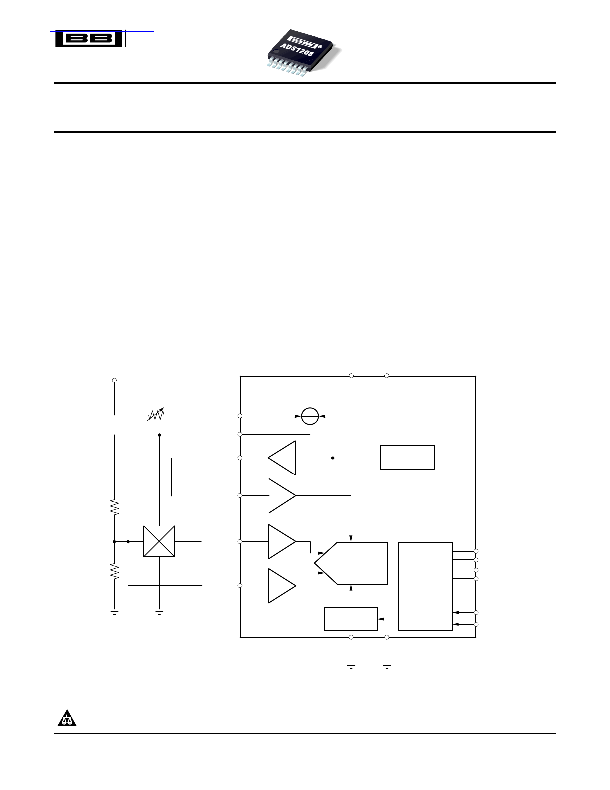
Internal 2.5V
Reference
RC Oscillator
20MHz
Interface
Circuit
MDATA
IADJ
IOUT
AVDD
ADS1208
REFOUT
REFIN
V
IN+
V
IN
−
MDATA
BVDD
MCLK
M0
M1
MCLK
Buffer
Buffer
Buffer
Buffer
2nd−Order
∆Σ
Modulator
BGNDAGND
AVDD
查询ADS1208供应商查询ADS1208供应商
SBAS348A – MARCH 2005 – REVISED MARCH 2005
2nd-Order Delta-Sigma Modulator
with Excitation for Hall Elements
FEATURES DESCRIPTION
• ±100mV Specified Input Range
• ±125mV Full-Scale Range
• 95dB typ. CMR, 82dB typ. SNR
• Adjustable Current Output for Sensor Biasing
• Digital Output Compatible to ADS1202/03 programmable current source for sensor biasing and
• Differential Digital Outputs
• Separate 2.7V to 5.5V Digital Supply Pin
APPLICATIONS
• Motor Control
• Current Measurement
• Hall Sensors
• Bridge Sensors
• Instrumentation
The ADS1208 is a 2nd-order ∆ Σ (delta-sigma) modulator operating at a 10MHz clock rate. The specified
input range is ±100mV, optimized for current
measurement with a Hall sensor, especially in motor
control applications. The ADS1208 contains a
has integrated input buffers for fast settling of the
sample capacitors; it also requires only a minimum of
external components. The differential analog input
offers low noise and excellent common-mode rejection.
ADS1208
Please be aware that an important notice concerning availability, standard warranty, and use in critical applications of Texas
Instruments semiconductor products and disclaimers thereto appears at the end of this data sheet.
PRODUCTION DATA information is current as of publication date.
Products conform to specifications per the terms of the Texas
Instruments standard warranty. Production processing does not
necessarily include testing of all parameters.
Copyright © 2005, Texas Instruments Incorporated
Page 2
www.ti.com
ADS1208
SBAS348A – MARCH 2005 – REVISED MARCH 2005
This integrated circuit can be damaged by ESD. Texas Instruments recommends that all integrated
circuits be handled with appropriate precautions. Failure to observe proper handling and installation
procedures can cause damage.
ESD damage can range from subtle performance degradation to complete device failure. Precision
integrated circuits may be more susceptible to damage because very small parametric changes could
cause the device not to meet its published specifications.
Package/Ordering Information
For the most current package and ordering information, see the Package Option Addendum at the end of this
document, or see the TI web site at www.ti.com .
ABSOLUTE MAXIMUM RATINGS
over operating free-air temperature range (unless otherwise noted)
Supply voltage, AGND to AV
Supply voltage, BGND to BV
Analog input voltage with respect to AGND AGND – 0.3 to AV
Reference input voltage with respect to AGND AGND – 0.3 to AV
Digital input voltage with respect to BGND BGND – 0.3 to BV
Ground voltage difference AGND to BGND ±0.3 V
Input current to any pin except supply ±10 mA
Power dissipation See Dissipation Ratings Table
Operating virtual junction temperature range, T
Operating free-air temperature range, T
Storage temperature range, T
(1) Stresses beyond those listed under Absolute Maximum Ratings may cause permanent damage to the device. These are stress ratings
only, and functional operation of the device at these or any other conditions beyond those indicated under Recommended Operating
Conditions is not implied. Exposure to absolute-maximum-rated conditions for extended periods may affect device reliability.
DD
DD
J
A
STG
(1)
ADS1208I UNIT
–0.3 to +6 V
–0.3 to +6 V
+ 0.3 V
DD
+ 0.3 V
DD
+ 0.3 V
DD
–40 to +150 °C
–40 to +85 °C
–65 to +150 °C
RECOMMENDED OPERATING CONDITIONS
PARAMETER MIN NOM MAX UNIT
Supply voltage, AGND to AV
Supply voltage, BGND to BV
DD
Low-voltage levels 2.7 3.6 V
DD
5V logic levels 4.5 5.0 5.5 V
4.5 5.0 5.5 V
Reference input voltage 0.5 2.5 3.0 V
Analog inputs V
– V
IN+
IN-
–V
/20 +V
REFIN
REFIN
/20 V
DISSIPATION RATINGS TABLE
BOARD PACKAGE R
(1)
Low-K
(2)
High-K
PW 35°C/W 147°C/W 6.8mW/°C 850mW 544mW 442mW
PW 33.6°C/W 108.4°C 9.225W/°C 1150mW 738mW 600mW
θ JC
R
(1) The JEDEC low-K (1s) board used to derive this data was a 3in x 3in, two-layer board with 2-ounce copper traces on top of the board.
(2) The JEDEC high-K (2s2p) board used to derive this data was a 3in x 3in, multilayer board with 1-ounce internal power and ground
planes and 2-ounce copper traces on top and bottom of the board.
2
DERATING FACTOR TA≤ 25°C TA= 70°C TA= 85°C
θ JA
ABOVE TA= 25°C POWER RATING POWER RATING POWER RATING
Page 3
www.ti.com
ADS1208
SBAS348A – MARCH 2005 – REVISED MARCH 2005
ELECTRICAL CHARACTERISTICS
Over recommended operating free-air temperature range at –40°C to +85°C, AV
Mode 3, MCLK input = 20MHz, differential input voltage = 200mV
, common-mode voltage = 1.4V, and 16-bit Sinc
PP
OSR = 256, unless otherwise noted.
PARAMETER TEST CONDITIONS MIN TYP
Resolution 16 Bits
DC Accuracy
Integral nonlinearity
Integral nonlinearity –0.012 0.0025 0.012 %
Differential nonlinearity
Input offset
(4)
Input offset drift 2.0 8.0 µV/°C
Gain error
(4)
Gain error drift Referenced to voltage at REFIN 15 ppm/°C
Power-supply rejection ratio 66 dB
Analog Input
Full-scale range V
Operating common-mode signal 0.8 1.4 2.5 V
Input capacitance 5.0 pF
Common-mode rejection 95 dB
Current Source (IOUT)
Output current
Voltage at IOUT pin V
Voltage between AVDD pin and IADJ V
Internal Voltage Reference
Reference output voltage REFOUT 2.45 2.5 2.55 V
Reference temperature drift 20 ppm/°C
Output resistance 0.3 Ω
Output source current 3.0 mA
Power-supply rejection ratio 60 dB
Startup time 0.1 ms
Voltage Reference Input
Reference voltage input REFIN 0.5 3.0 V
Reference input capacitance 5 pF
Reference input current -50 +50 nA
Internal Clock for Modes 0, 1 and 2
Clock frequency 8.0 10.1 12.0 MHz
External Clock for Mode 3
Clock frequency 1.0 24.0 MHz
(1) All values are at TA= 25°C.
(2) Integral nonlinearity is defined as the maximum deviation of the line through the end points of the specified input range of the transfer
curve for V
(200mV).
(3) Ensured by design.
(4) Maximum values, including temperature drift, are ensured over the full specified temperature range.
(5) It is possible to leave pin IOUT unconnected (I
(2)
(3)
16-bit resolution –8 1.6 8 LSB
16-bit resolution –1.0 1.0 LSB
Referenced to voltage at REFIN –1.25 –0.7 1.25 %
– V
IN+
IN–
(5)
ADJ
– V
IN+
= –100mV to +100mV, expressed either as the number of LSBs or as a percent of the measured input range
IN–
= 0mA).
OUT
I
OUT
OUT
at I
= 1mA to 8mA 480 500 520 mV
OUT
= BV
DD
DD
= +5V, V
= internal +2.5V,
REF
ADS1208I
(1)
–2.0 –1.4 0 mV
–125 125 mV
1.0 5.0 8.0 mA
0 AVDD – 1.0 V
3
MAX UNIT
filter with
3
Page 4
www.ti.com
ADS1208
SBAS348A – MARCH 2005 – REVISED MARCH 2005
ELECTRICAL CHARACTERISTICS (continued)
Over recommended operating free-air temperature range at –40°C to +85°C, AV
Mode 3, MCLK input = 20MHz, differential input voltage = 200mV
, common-mode voltage = 1.4V, and 16-bit Sinc
PP
OSR = 256, unless otherwise noted.
PARAMETER TEST CONDITIONS MIN TYP
AC Accuracy
SNR VIN= 200mV
SINAD VIN= 200mV
THD VIN= 200mV
SFDR VIN= 200mV
Digital Inputs
(6)
Logic family CMOS
V
High-level input voltage 0.7 x BV
IH
V
Low-level input voltage –0.3 0.3 x BV
IL
I
Input current VIN= BV
IN
C
Input capacitance 5 pF
I
Digital Outputs
(6)
Logic family CMOS
V
High-level output voltage BV
OH
V
Low-level output voltage BV
OL
C
Load capacitance 30 pF
L
= 4.5V, IOH= –100µA 4.44 V
DD
= 4.5V, IOL= +100µA 0.5 V
DD
Data format Bit stream
Digital Inputs
(7)
Logic family LVCMOS
V
High-level input voltage BV
IH
V
Low-level input voltage BV
IL
I
Input current VIN= BV
IN
C
Input capacitance 5 pF
I
Digital Outputs
(7)
Logic family LVCMOS
V
High-level output voltage BV
OH
V
Low-level output voltage BV
OL
C
Load capacitance 30 pF
L
= 2.7, IOH= –100µA BV
DD
= 2.7, IOL= +100µA 0.2 V
DD
Data format Bit stream
Power Supply
Analog supply voltage, AV
Digital interface supply voltage, BV
Operating supply current, AI
Operating supply current, AI
Operating supply current, BI
Operating supply current, BI
DD
DD
DD
DD
DD
DD
Modes 0, 1 and 2 11.9 15.0 mA
Modes 0, 1 and 2 2.3 3.0 mA
Power dissipation Modes 0, 1 and 2 71 90 mW
Power dissipation Mode 3 64 82.5 mW
(6) Applicable for 5.0V nominal supply; BV
(7) Applicable for 3.0V nominal supply; BV
(min) = 4.5V and BV
DD
(min) = 2.7V and BV
DD
at 1kHz 80 82 dB
PP
at 1kHz 77 81.5 dB
PP
at 1kHz –91 –80 dB
PP
at 1kHz 80 93 dB
PP
or GND –50 50 nA
DD
= 3.6V 2 BV
DD
= 2.7V –0.3 0.8 V
DD
or GND –50 50 nA
DD
Mode 3 11.5 14.5 mA
Mode 3 1.3 2.0 mA
(max) = 5.5V.
DD
(max) = 3.6V
DD
= BV
DD
DD
= +5V, V
= internal +2.5V,
REF
ADS1208I
(1)
DD
– 0.2 V
DD
BV
DD
DD
4.5 5.0 5.5 V
2.7 5 5.5 V
MAX UNIT
+ 0.3 V
DD
+ 0.3 V
3
filter with
V
4
Page 5
www.ti.com
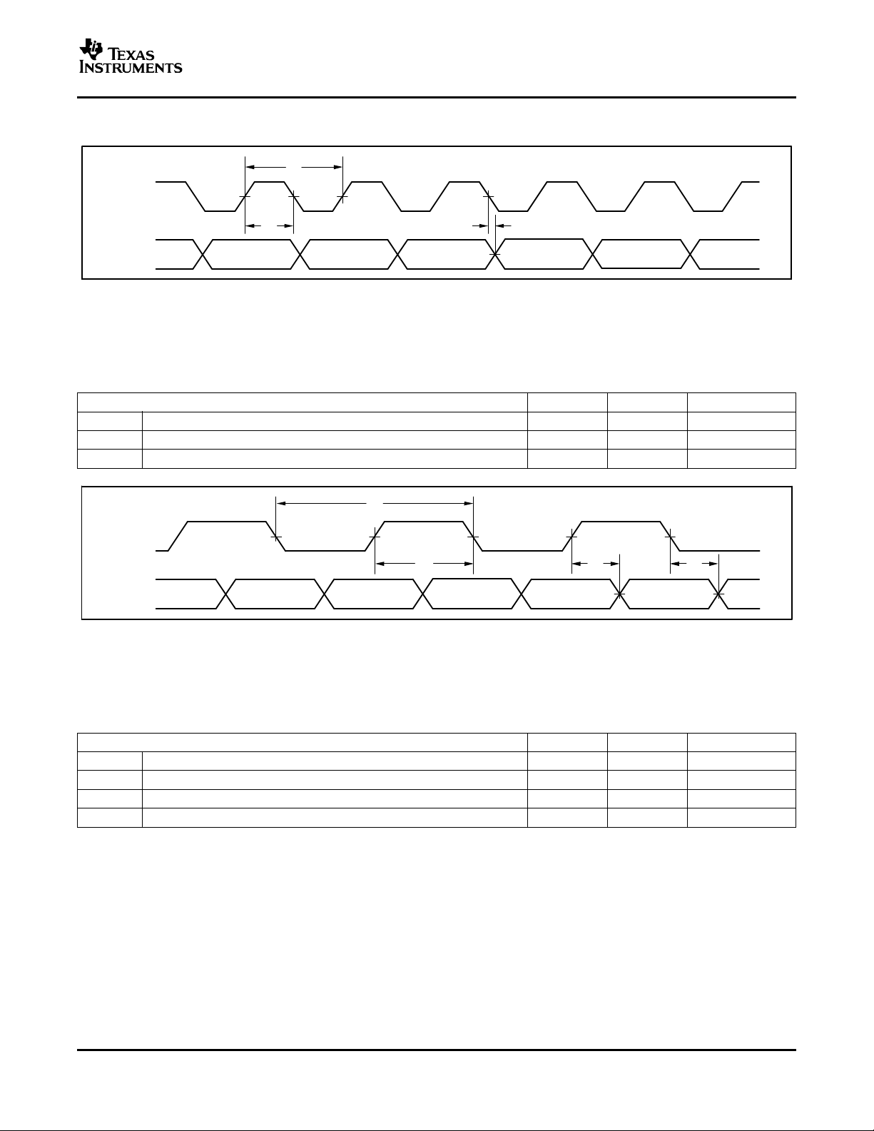
MCLK
MDATA
t
C1
t
W1
t
D1
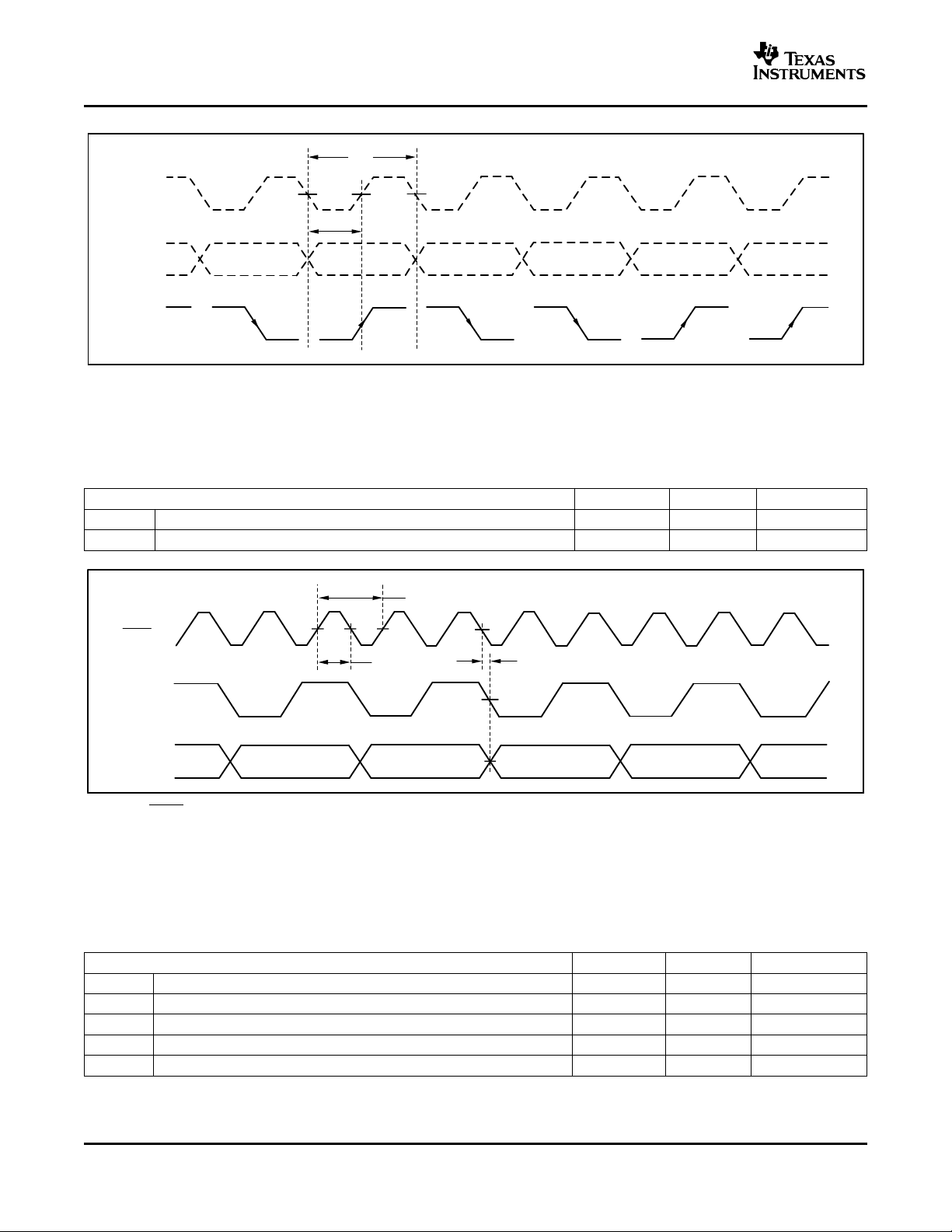
MCLK
MDATA
t
C2
t
W2
t
D2
t
D3
PARAMETER MEASUREMENT INFORMATION
Figure 1. Mode 0 Operation
TIMING CHARACTERISTICS: MODE 0
Over recommended operating free-air temperature range at –40°C to +85°C, and AV
otherwise noted.
PARAMETER MIN MAX UNIT
t
C1
t
W1
t
D1
Clock period 83 125 ns
Clock high time (tC1/2) – 5 (tC1/2) + 5 ns
Data delay after rising edge of clock –2 +2 ns
ADS1208
SBAS348A – MARCH 2005 – REVISED MARCH 2005
= +5V, BV
DD
= +2.7 to +5.5V, unless
DD
Figure 2. Mode 1 Operation
TIMING CHARACTERISTICS: MODE 1
Over recommended operating free-air temperature range at –40°C to +85°C, and AV
otherwise noted.
PARAMETER MIN MAX UNIT
t
C1
t
W2
t
D2
t
D3
Clock period 166 250 ns
Clock high time (tC2/2) – 5 (tC2/2) + 5 ns
Data delay after rising edge of clock (t
Data delay after falling edge of clock (t
= +5V, BV
DD
/2) – 2 (t
W2
/2) – 2 (t
W2
DD
/2) + 2 ns
W2
/2) + 2 ns
W2
= +2.7 to +5.5V, unless
5
Page 6
www.ti.com
Internal
MCLK
Internal
MDATA
MDATA
t
C1
t
W 1
1 0 1 1 0 0
MDAT
MCLK
t
C4
t
W 4
t
D4
MCLK
ADS1208
SBAS348A – MARCH 2005 – REVISED MARCH 2005
Figure 3. Mode 2 Operation
TIMING CHARACTERISTICS: MODE 2
Over recommended operating free-air temperature range at –40°C to +85°C, and AV
otherwise noted.
PARAMETER MIN MAX UNIT
t
C1
t
W1
Clock period 83 125 ns
Clock high time (tC1/2) – 5 (tC1/2) + 5 ns
= +5V, BV
DD
= +2.7 to +5.5V, unless
DD
note: MCLK is system clock input. MCLK is modulator clock output. Modulator clock frequency is half of system clock
frequency.
Figure 4. Mode 3 Operation
TIMING CHARACTERISTICS: MODE 3
Over recommended operating free-air temperature range at –40°C to +85°C, and AV
otherwise noted.
PARAMETER MIN MAX UNIT
t
C4
t
W4
t
D4
t
R
t
F
6
Clock period 41 1000 ns
Clock high time 10 tC4– 10 ns
Data and output clock delay after falling edge of input clock 0 10 ns
Rise time of clock (10% to 90% of BV
Fall time of clock (90% to 10% of BV
) 0 10 ns
DD
) 0 10 ns
DD
= +5V, BV
DD
DD
= +2.7 to +5.5V, unless
Page 7
www.ti.com
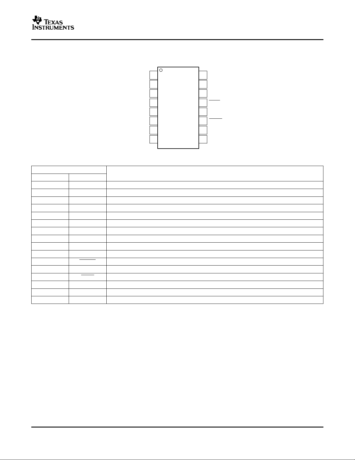
DEVICE INFORMATION
1
2
3
4
16
15
14
13
BVDD
BGND
MCLK
MCLK
12
11
10
9
MDATA
MDATA
M0
M1
ADS1208
(TOP VIEW)
IOUT
IADJ
AVDD
V
IN+
V
IN−
AGND
REFIN
REFOUT
5
6
7
8
16-LEAD TSSOP PACKAGE
Table 1. TERMINAL FUNCTIONS
PIN
NO. NAME
1 IOUT Current output for sensor
2 IADJ Output current adjustment
3 AVDD Analog supply
4 V
5 V
IN+
IN–
6 AGND Analog ground
7 REFIN Reference input
8 REFOUT Reference output
9 M1 Mode selection input
10 M0 Mode selection input
11 MDATA Inverted data output
12 MDATA Noninverted data output
13 MCLK Inverted clock output (Modes 0, 1); Clock input (Mode 3)
14 MCLK Noninverted clock output
15 BGND Digital interface ground
16 BVDD Digital interface supply (2.7V to 5.5V)
DESCRIPTION
Positive input
Negative input
ADS1208
SBAS348A – MARCH 2005 – REVISED MARCH 2005
7
Page 8

www.ti.com
ADS1208
IOUT
IADJ
AVDD
V
IN+
V
IN
−
AGND
REFIN
REFOUT
BVDD
BGND
MCLK
MCLK
MDATA
MDATA
M0
M1
1k
Ω
100nF 10µF
R
2
R
1
R
4
R
3
R
ADJ
100nF
10µF 100nF
Hall Element
+5V
+5V
ADS1208
SBAS348A – MARCH 2005 – REVISED MARCH 2005
FUNCTIONAL BLOCK DIAGRAM
A. For Functional configuration (Mode 0), possible Hall elements include the Toshiba THS119 and the Philips KMZ10.
Figure 5. Functional Configuration (Mode 0)
8
Page 9

www.ti.com
Differential Input Signal (mV)
INL (LSB)
0
−
100 100
−
80 80
−
60 60
−
40 40
−
20 20
6
5
4
3
2
1
0
−
1
−
2
+25C
−
40C
+85C
Differential Input Signal (mV)
INL (LSB)
0
−
100 100
−
80 80
−
60 60
−
40 40
−
20 20
4
3
2
1
0
−
1
−
2
−
3
−
4
+25C
−
40C
+85C
Temperature (C)
INL (LSB)
0
−
40 +80+60+40
−
20 +20
6
5
4
3
2
1
0
M0
M3
Temperature (C)
Gain Error (%)
0
−
40 +80+60+40
−
20 +20
0
−
0.1
−
0.2
−
0.3
−
0.4
−
0.5
−
0.6
−
0.7
−
0.8
M0
M3
Temperature (C)
Offset (mV)
0
−
40 +80+60+40
−
20 +20
0
−
0.2
−
0.4
−
0.6
−
0.8
−
1.0
−
1.2
−
1.4
−
1.6
M0
M3
Power Supply (V)
Offset (mV)
4.50 4.75 5.00 5.25 5.50
0
−
0.2
−
0.4
−
0.6
−
0.8
−
1.0
−
1.2
−
1.4
−
1.6
−
1.8
M0
M3
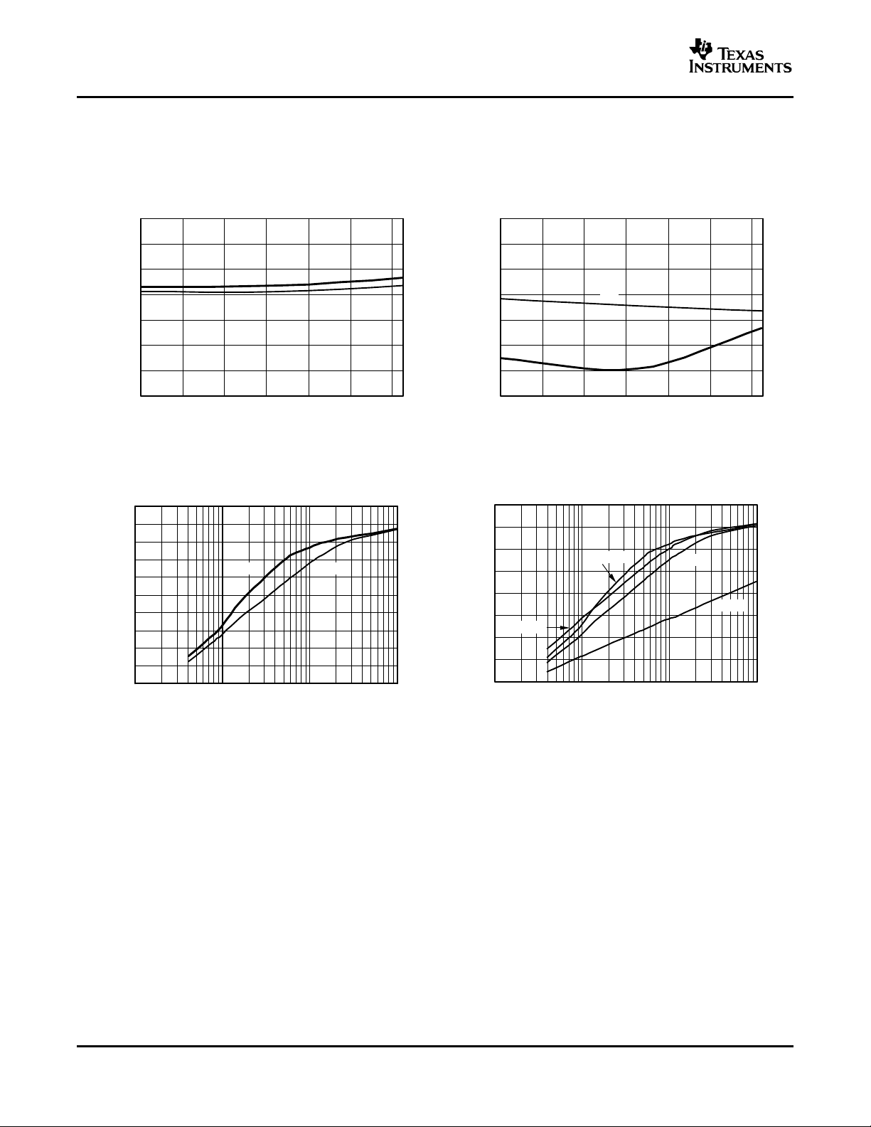
At 25°C, AV
SBAS348A – MARCH 2005 – REVISED MARCH 2005
TYPICAL CHARACTERISTICS
= BV
DD
common-mode voltage = 1.4V, and 16-bit Sinc
DD
= +5V, V
= internal +2.5V, Mode 3, MCLK input = 20MHz, differential input voltage = 200mV
REF
3
filter with OSR = 256, unless otherwise noted.
INTEGRAL NONLINEARITY vs INTEGRAL NONLINEARITY vs
INPUT SIGNAL (Mode 0) INPUT SIGNAL (Mode 3, MCLK = 20MHZ)
Figure 6. Figure 7.
ADS1208
,
PP
INTEGRAL NONLINEARITY vs GAIN ERROR vs
TEMPERATURE TEMPERATURE
Figure 8. Figure 9.
OFFSET vs OFFSET vs
TEMPERATURE POWER SUPPLY
Figure 10. Figure 11.
9
Page 10
www.ti.com
Temperature (C)
SNR (dB)
0
−
40 +80+60+40
−
20 +20
85
84
83
82
81
80
79
78
M0
M3
Temperature (C)
SINAD (dB)
0
−
40 +80+60+40
−
20 +20
85
84
83
82
81
80
79
78
M0
M3
Decimation Ratio (OSR)
ENOB (BIts)
1 10 100 1000
16
14
12
10
8
6
4
2
0
Sinc1
Sinc2
Sinc3
Sincfast
Decimation Ratio (OSR)
SNR (dB)
1 10 100 1000
100
90
80
70
60
50
40
30
20
10
0
Sinc2Sinc3
ADS1208
SBAS348A – MARCH 2005 – REVISED MARCH 2005
TYPICAL CHARACTERISTICS (continued)
At 25°C, AV
common-mode voltage = 1.4V, and 16-bit Sinc
= BV
DD
DD
= +5V, V
= internal +2.5V, Mode 3, MCLK input = 20MHz, differential input voltage = 200mV
REF
SIGNAL-TO-NOISE RATIO vs SIGNAL-TO-NOISE AND DISTORTION vs
TEMPERATURE TEMPERATURE
Figure 12. Figure 13.
3
filter with OSR = 256, unless otherwise noted.
,
PP
SIGNAL-TO-NOISE RATIO vs EFFECTIVE NUMBER OF BITS vs
DECIMATION RATIO DECIMATION RATIO
Figure 14. Figure 15.
10
Page 11

www.ti.com
Temperature (C)
SFDR (dB)
0
−
40 +80+60+40
−
20 +20
105
100
95
90
85
80
SFDR
THD
−
105
−
100
−
95
−
90
−
85
−
80
THD (dB)
Temperature (C)
SFDR (dB)
0
−
40 +80+60+40
−
20 +20
105
100
95
90
85
80
SFDR
THD
−
105
−
100
−
95
−
90
−
85
−
80
THD (dB)
f
SIG
(kHz)
SFDR (dB)
0 5 1510 20
105
100
95
90
85
80
SFDR
THD
−
105
−
100
−
95
−
90
−
85
−
80
THD (dB)
f
SIG
(kHz)
SFDR (dB)
0 5 1510 20
105
100
95
90
85
80
SFDR
THD
−
105
−
100
−
95
−
90
−
85
−
80
THD (dB)
TYPICAL CHARACTERISTICS (continued)
At 25°C, AV
common-mode voltage = 1.4V, and 16-bit Sinc
= BV
DD
DD
= +5V, V
= internal +2.5V, Mode 3, MCLK input = 20MHz, differential input voltage = 200mV
REF
SPURIOUS-FREE DYNAMIC RANGE AND SPURIOUS-FREE DYNAMIC RANGE AND
TOTAL HARMONIC DISTORTION vs TOTAL HARMONIC DISTORTION vs
FREQUENCY (Mode 1) TEMPERATURE (Mode 3)
Figure 16. Figure 17.
3
filter with OSR = 256, unless otherwise noted.
ADS1208
SBAS348A – MARCH 2005 – REVISED MARCH 2005
,
PP
SPURIOUS-FREE DYNAMIC RANGE AND SPURIOUS-FREE DYNAMIC RANGE AND
TOTAL HARMONIC DISTORTION vs TOTAL HARMONIC DISTORTION vs
FREQUENCY (Mode 1) TEMPERATURE (Mode 3)
Figure 18. Figure 19.
11
Page 12

www.ti.com
Frequency (kHz)
Magnitude (dB)
0 5 1510 20
0
−
20
−
40
−
60
−
80
−
100
−
120
−
140
Frequency (kHz)
Magnitude (dB)
0 5 1510 20
0
−
20
−
40
−
60
−
80
−
100
−
120
−
140
Frequency (kHz)
CMRR (dB)
1 10 100 1000
110
105
100
95
90
85
80
75
70
65
60
M0
M3
Frequency (kHz)
PSRR (dB)
0.1 1 10 100 1000
90
85
80
75
70
65
60
55
50
M0
M3
Temperature (C)
MCLK (MHz)
0
−
40 +80+60+40
−
20 +20
10.6
10.5
10.4
10.3
10.2
10.1
10.0
9.9
9.8
9.7
9.6
VDD(V)
MCLK (MHz)
4.50 4.75 5.255.00 5.50
10.20
10.15
10.10
10.05
10.00
9.95
ADS1208
SBAS348A – MARCH 2005 – REVISED MARCH 2005
TYPICAL CHARACTERISTICS (continued)
At 25°C, AV
common-mode voltage = 1.4V, and 16-bit Sinc
= BV
DD
DD
= +5V, V
= internal +2.5V, Mode 3, MCLK input = 20MHz, differential input voltage = 200mV
REF
FREQUENCY SPECTRUM FREQUENCY SPECTRUM
(4096 POINT FFT, fIN= 1kHz) (4096 POINT FFT, fIN= 5kHz)
Figure 20. Figure 21.
3
filter with OSR = 256, unless otherwise noted.
,
PP
COMMON-MODE REJECTION RATIO vs POWER-SUPPLY REJECTION RATIO vs
FREQUENCY FREQUENCY
Figure 22. Figure 23.
CLOCK FREQUENCY vs CLOCK FREQUENCY vs
TEMPERATURE POWER SUPPLY
12
Figure 24. Figure 25.
Page 13

www.ti.com
Temperature (C)
I
DD
(mA)
0
−
40 +80+60+40
−
20 +20
14
13
12
11
10
9
8
M0
M3
Temperature (C)
I
DD
(mA)
0
−
40 +80+60+40
−
20 +20
3.0
2.5
2.0
1.5
1.0
0.5
0
M0
M3
Temperature (C)
V
REF
(V)
0
−
40 +80+60+40
−
20 +20
2.5000
2.4998
2.4996
2.4994
2.4992
2.4990
2.4988
2.4986
2.4984
2.4982
2.4980
VDD(V)
V
REF
(V)
3.0 4.03.5 5.04.5 5.5 6.0
2.5000
2.4998
2.4996
2.4994
2.4992
2.4990
2.4988
2.4986
2.4984
2.4982
2.4980
I
OUT
(mA)
V
REF
(V)
−
5 50 1510 20
2.525
2.520
2.515
2.510
2.505
2.500
2.495
2.490
2.485
2.480
2.475
5.5V
5.0V
4.5V
V
OUT
(V)
V
REF
(mV)
0 21 43 65
499.2
499.1
499.0
498.9
498.8
498.7
498.6
498.5
498.4
498.3
498.2
VDD= 5.0V
V
DD
= 4.5V
VDD= 5.5V
TYPICAL CHARACTERISTICS (continued)
At 25°C, AV
common-mode voltage = 1.4V, and 16-bit Sinc
= BV
DD
DD
= +5V, V
= internal +2.5V, Mode 3, MCLK input = 20MHz, differential input voltage = 200mV
REF
3
filter with OSR = 256, unless otherwise noted.
ADS1208
SBAS348A – MARCH 2005 – REVISED MARCH 2005
,
PP
ANALOG POWER SUPPLY CURRENT vs DIGITAL POWER SUPPLY CURRENT vs
TEMPERATURE TEMPERATURE
Figure 26. Figure 27.
REFERENCE OUTPUT VOLTAGE vs REFERENCE OUTPUT VOLTAGE vs
TEMPERATURE POWER SUPPLY
REFERENCE OUTPUT VOLTAGE vs CURRENT SOURCE REFERENCE VOLTAGE vs
LOAD CURRENT LOAD VOLTAGE (I = 8mA)
Figure 28. Figure 29.
Figure 30. Figure 31.
13
Page 14

www.ti.com
Temperature (C)
V
ADJ
(mV)
0
−
40 +80+60+40
−
20 +20
499.2
499.1
499.0
498.9
498.8
498.7
498.6
498.5
498.4
498.3
498.2
VDD(V)
V
ADJ
(mV)
4.00 5.254.25 5.004.50 5.50 6.005.754.75
499.2
499.1
499.0
498.9
498.8
498.7
498.6
498.5
498.4
498.3
498.2
Differential Input Voltage (V)
RMS Noise (
µ
V)
−
125−100−75−50−25 1250 25 7550 100
10
9
8
7
6
5
4
3
2
1
0
ADS1208
SBAS348A – MARCH 2005 – REVISED MARCH 2005
TYPICAL CHARACTERISTICS (continued)
At 25°C, AV
common-mode voltage = 1.4V, and 16-bit Sinc
= BV
DD
DD
= +5V, V
= internal +2.5V, Mode 3, MCLK input = 20MHz, differential input voltage = 200mV
REF
3
filter with OSR = 256, unless otherwise noted.
,
PP
CURRENT SOURCE REFERENCE VOLTAGE vs CURRENT SOURCE REFERENCE VOLTAGE vs
TEMPERATURE (I = 8mA) POWER SUPPLY (I = 8mA)
Figure 32. Figure 33.
RMS NOISE vs
INPUT VOLTAGE LEVEL
14
Figure 34.
Page 15

www.ti.com
Delta−Sigma
Modulator
AZ
AVDD
V
IN+
V
IN
−
AZ
ADS1208
SBAS348A – MARCH 2005 – REVISED MARCH 2005
APPLICATION INFORMATION
should be used at the output of the delta-sigma
GENERAL DESCRIPTION
The ADS1208 is a 2nd-order delta-sigma modulator,
which is implemented with a switched capacitor
circuit. The analog input signal is continuously
sampled by the modulator and compared to an
internal voltage reference. A digital bit stream, which
accurately represents the analog input voltage over
time, appears at the output of the converter.
The ADS1208 is optimized for Hall sensors and
similar applications. As a result, the full-scale input
range is ±V
/20, which is typically ±125mV. How-
REFIN
ever, to achieve good noise and linearity, only 80% of
this range should be used (±100mV). The analog
input pins (V
and V
IN+
) are internally buffered with
IN-
two low-noise, high bandwidth, low offset amplifiers.
A current source is also integrated into the ADS1208
that can be used for biasing a Hall element or bridge
sensor. This current can be programmed with a
resistor that must be placed between AVDD and
IADJ.
Additionally, the ADS1208 includes a reference voltage source with a buffered output. A reference input
pin is provided as well. The voltage at the REFIN pin
sets the analog input range.
The device digital interface is fully compatible with the
ADS1202 and ADS1203. The ADS1208 also provides
inverted outputs of MCLK and MDATA ( MCLK and
MDATA, respectively) to increase noise immunity for
the digital data transmission.
The clock source can be internal as well as external.
Different clock frequencies in combination with an
optional digital filter enable a variety of solutions and
signal bandwidths.
Figure 5 (page 8) shows the functional block diagram
with external circuitry. The Hall element is biased
from the internal current source. The current is set by
resistor R
. An offset compensation of the Hall
ADJ
element is enabled by the optional resistors R1 to R4.
The analog inputs V
and V
IN+
are directly connec-
IN–
ted with the Hall element outputs. The reference input
REFIN is connected to the reference output REFOUT
with an optional RC low-pass filter, for additional
noise filtering. For both power-supply pairs, AVDD
and BVDD, decoupling capacitors of 100nF and 10µF
(respectively) are recommended.
ANALOG SECTION
Modulator
The 2nd-order modulator acts as a filter. The input
signal is low-passed while the quantization noise is
shifted to higher frequencies. A digital low-pass filter
modulator. The primary purpose of the digital filter is
to remove high-frequency noise. The secondary purpose is to convert the 1-bit data stream at a high
sampling rate into a higher-bit data word at a lower
rate (that is, decimation). A digital signal processor
(DSP), microcontroller (µC), or field programmable
gate array (FPGA) could be used to implement the
digital filter.
Analog Inputs
The internal sampling capacitors present a very
significant load that needs to be recharged within
50ns. The ADS1208 provides two input buffers to
decouple the sampling capacitors from the pins (V
V
). These buffers provide a high bandwidth
IN–
(typically, 50MHz) at a low noise and low offset. This
configuration improves the system performance significantly, if the input source has a high impedance in
the k Ω range. A source impedance in this range
without buffers would decrease THD and linearity
significantly, and would also cause a gain error that
changes with supply or temperature.
The input buffers have an auto zero function to
reduce the input offset. The auto zero switches of the
input buffers may apply a glitch of 10fC to 50fC to the
signal source in each clock cycle. For this reason,
placing a 1nF capacitor between the inputs is recommended, if the source impedance is larger than
500 Ω . See Figure 35 for the equivalent input circuit,
including the protection diodes.
Figure 35. Equivalent Input Circuit
Internal Reference
The ADS1208 includes a 2.5V reference. The reference output is connected to the REFOUT pin via an
output buffer that can source 3mA. The sink current is
limited to 50µA. The output resistance of this buffer is
0.3 Ω . The internal reference is also used to control
the current source at the IOUT pin.
The ADS1208 additionally provides a REFIN pin. The
applied voltage V
sets the gain of the internal
REFIN
,
IN+
15
Page 16

www.ti.com
Y
OUT
1
R
ADJ
V
IADJ
AVDD
V
REFOUT
5
RI= 0.3
Ω
AVDD
IADJ
IOUT
V
REF
/5
R
ADJ
e.g., 100
Ω
for 5mA
+5V
R
OUT
V
ADJ
= 0.5V
V
ADJ
V
REFOUT
5
0.5 V
I
OUT
V
REFOUT
5 R
ADJ
0.3
Modulator Output
Analog Input
+FS (Analog Input)
−
FS (Analog Input)
ADS1208
SBAS348A – MARCH 2005 – REVISED MARCH 2005
modulator. An external reference could vary from also directly proportional to the reference voltage, the
0.5V to 3V. The modulator input range is defined to drift of the reference is actually cancelled out. Be
±V
is ±125mV. The REFIN pin is decoupled from the using IOUT to drive the Hall sensor and if REFIN is
modulator with a buffer. connected to REFOUT.
Current Source for the Hall Element
Internal circuitry (see Figure 36 ) forces the IADJ pin
to a potential of:
/20. For a 2.5V reference, the full-scale range aware that this is only the case if the application is
REFIN
This means that trimming the resistor can calibrate
the gain of the entire system. The resistor can be
chosen to be stable over temperature, or to compensate any temperature behavior of the Hall sensor.
DIGITAL OUTPUT
A differential analog input signal of 0V ideally produces a stream of 1s and 0s that are high 50% of the
time and low 50% of the time. A differential analog
input of +100mV produces a stream of 1s and 0s that
are high 80% of the time. A differential analog input
of –100mV produces a stream of 1s and 0s that are
high 20% of the time. The input voltage versus the
output modulator signal is shown in Figure 37 .
Figure 36. Current Source
This means that the voltage drop of the resistor R
is equal to the current source reference V
With resistor R
placed between AVDD and IADJ, a
ADJ
.
ADJ
current of:
is sourced out of the IOUT pin. The current should be
set between 1mA and 8mA. However, it is also
possible to leave the pin open. As the Hall voltage is
directly proportional to this current, the input voltage
to the modulator V
internal reference voltage V
digital output data word Y
is directly proportional to the
IN
OUT
. As the filtered
REFOUT
from the modulator is
DIGITAL INTERFACE
Introduction
ADJ
The analog signal that is connected to the input of the
delta-sigma modulator is converted using the clock
signal that is applied to the modulator. The result of
the conversion, or modulation, is the output signal
MDATA from the delta-sigma modulator. In most
applications, the two standard signals (MCLK and
MDATA) are provided from the modulator to an ASIC,
FPGA, DSP, or µC (each with an implemented filter,
respectively). A single wire interface is provided in
Mode 2, where the data stream is Manchester
encoded. This configuration reduces the costs for
galvanic isolation.
The interface also provides the inverted outputs
MDATA and MCLK for the signals MDATA and
MCLK, respectively. These inverted outputs are useful for systems with high common-mode noise at the
digital data transmission. The digital interface is
specified for the voltage range of 2.7V to 5.5V.
16
Figure 37. Analog Input vs Modulator Output of the ADS1208
Page 17

www.ti.com
H(z)
1z
OSR
1z
1
3
ADS1208
SBAS348A – MARCH 2005 – REVISED MARCH 2005
Different Modes of Operation
The typical system clock of the ADS1208 is 20MHz.
The system clock can be provided either from the
internal 20MHz RC oscillator or from an external
clock source. For this reason, the MCLK pin is
bidirectional and is controlled by the mode setting.
The system clock is divided by two for the modulator
clock. Therefore, the default clock frequency of the
modulator is 10MHz. With a possible external clock
range of 1MHz to 24MHz, the modulator operates
between 500kHz and 12MHz. The four modes of
operation for the digital data interface are shown in
Table 2 .
Mode 0
In Mode 0, the internal RC oscillator is running. The
data is provided at the MDATA and MDATA output
pins, and the modulator clock at the MCLK and
MCLK pins. The data changes at the falling edge of
MCLK. Therefore, it can safely be strobed with the
rising edge. See Figure 1 on page 5.
Mode 1
In Mode 1, the internal RC oscillator is running. The
data is provided at the MDATA and MDATA output
pins. The frequency at the MCLK and MCLK pins is
equivalent to the modulator clock frequency divided
by two. The data must be strobed at both the rising
and falling edges of MCLK. The data at MDATA
changes in the middle, between the rising and falling
edge. In this mode, the frequency of both MCLK and
MDATA is only 5MHz. See Figure 2 on page 5.
Mode 2
In Mode 2, the internal RC oscillator is running. The
data is Manchester encoded and is provided at the
MDATA and MDATA pins. There is no clock output in
this mode. The MCLK and MCLK outputs are set to
low. The Manchester coding allows the data transfer
with only a single wire. See Figure 3 on page 6.
Mode 3
In Mode 3, the internal RC oscillator is disabled. The
system clock must be provided externally at the input
MCLK. The system clock must have twice the frequency of the chosen modulator clock. The data is
provided at the MDATA and MDATA output pins.
Since the modulator runs with half the frequency of
the system clock, the data changes at every other
falling edge of the external clock. The data can be
safely strobed at every rising edge of the MCLK
output, which provides half the frequency of the
system clock. This mode allows synchronous operation to any digital system or the use of modulator
clocks different from 10MHz. See Figure 4 on page 6.
Filter Usage
The modulator generates only a bitstream, which is
different from the digital word of an analog-to-digital
converter (ADC). In order to output a digital word
equivalent to the analog input voltage, the bitstream
must be processed by a digital filter. A very simple
filter built with minimal effort and hardware is the
3
Sinc
filter, shown in Equation 1 :
(1)
Table 2. Operating Mode Definition and Description
MODE DEFINITION M1 M0
Mode 0 Internal clock, synchronous data output Low Low
Mode 1 Internal clock, synchronous data output, half output clock frequency Low High
Mode 2 Internal clock, Manchester encoded data output, no clock output High Low
Mode 3 External clock, synchronous data output High High
17
Page 18

www.ti.com
Decimation Ratio (OSR)
ENOB (BIts)
1 10 100 1000
16
14
12
10
8
6
4
2
0
Sinc1
Sinc2
Sinc3
Sincfast
0
−
10
−
20
−
30
−
40
−
50
−
60
−
70
−
80
Gain (dB)
Frequency (kHz)
0 200 400 600 800 1000 1200 1400 1600
OSR = 32
fDATA = 10MHz/32 = 312.5kHz
−
3dB: 81.9kHz
H(z)
1z
OSR
1z
1
2
1z
2OSR
10
9
8
7
6
5
4
3
2
1
0
ENOB (Bits)
Settling Time (µs)
1 2 3 4 5 6 7 8 90 10
Sinc
2
Sinc
Sinc
3
Sincfast
30k
25k
20k
15k
10k
5k
0
Output Code
Number of Output Clocks
0 5 10 15 20 25 30 35 40
OSR = 32
FSR = 32768
ENOB = 9.9 Bits
Settling Time =
3×1/fDATA = 9.6µs
ADS1208
SBAS348A – MARCH 2005 – REVISED MARCH 2005
This filter provides the best output performance at the
lowest hardware size (for example, a count of digital
gates). For oversampling ratios in the range of 16 to
256, the Sinc
characterizations in this datasheet were obtained
using a Sinc
of 256 and an output word length of 16 bits. In a
3
Sinc
filter response (shown in Figure 38 and Figure 39 ), the location of the first notch occurs at the
frequency of output data rate f
–3dB point is located at half the Nyquist frequency, or
f
/4. For some applications, it may be necessary
DATA
to use another filter type for better frequency response. Device performance can be improved, for
example, by using a cascaded filter structure. The
first decimation stage can be a Sinc
OSR and a second stage, high-order filter.
3
filter is a good choice. All
3
filter with an oversampling ratio (OSR)
DATA
= f
CLK
3
filter with a low
/OSR. The
Figure 40. Measured ENOB vs OSR
In motor control applications, a very fast response
time for overcurrent detection is required. There is a
constraint between 1µs and 5µs with 3 bits to 7 bits
of resolution. The time for full settling depends on the
filter order. Therefore, the full settling of the Sinc
filter needs three data clocks and the Sinc
2
needs two data clocks. The data clock is equal to the
modulator clock divided by the OSR. For overcurrent
protection, filter types other than Sinc
better choice. A good example is a Sinc
Figure 41 compares the settling time of different filter
types. The Sincfast is a modified Sinc
3
might be a
2
filter, as
2
filter.
shown in Equation 2 :
3
filter
Figure 38. Frequency Response of Sinc
Figure 39. Pulse Response of Sinc
(f
The effective number of bits (ENOB) can be used to
compare the performance of ADCs and delta-sigma
modulators. Figure 40 shows the ENOB of the
ADS1208 with different filter types. In this datasheet,
the ENOB is calculated from the SNR:
SNR = 1.76dB + 6.02dB × ENOB
18
MOD
= 10MHz)
3
Filter
3
Filter
Figure 41. Measured ENOB vs Settling Time
(2)
For more information, see application note SBAA094 ,
Combining the ADS1202 with an FPGA Digital Filter
for Current Measurement in Motor Control Applications, available for download at www.ti.com .
Page 19

www.ti.com
ADS1208
SBAS348A – MARCH 2005 – REVISED MARCH 2005
LAYOUT CONSIDERATIONS
Power Supplies
The ADS1208 has two power supplies, AVDD and
BVDD. If there are separate analog and digital power
supplies on the board, a good design approach is to
have AVDD connected to the analog and BVDD to
the digital power supply. Another possible approach
to control noise is the use of a resistor on the power
supply. The connection can be made between the
ADS1208 power supply pins via a 5 Ω resistor. The
combination of this resistor and the decoupling ca-
Grounding
Analog and digital sections of the system design must
be carefully and cleanly partitioned. Each section
should have its own ground plane, with no overlap
between them. Do not join the ground planes. Instead, connect the two planes with a moderate signal
trace underneath the modulator. For multiple modulators, connect the two ground planes as close as
possible to one central location for all of the modulators. In some cases, experimentation may be required to find the best point to connect the two planes
together.
pacitors between the power supply pins AVDD and
AGND provides some filtering. The analog supply
must be well-regulated and offer low noise. For
designs requiring higher resolution from the
ADS1208, power-supply rejection will be a concern.
The digital power supply has high-frequency noise
that can be coupled into the analog portion of the
ADS1208. This noise can originate from switching
power supplies, microprocessors, or DSPs.
High-frequency noise will generally be rejected by the
external digital filter at integer multiples of MCLK.
Just below and above these frequencies, noise will
alias back into the passband of the digital filter,
Decoupling
Good decoupling practices must be used for the
ADS1208 and for all components in the system
design. All decoupling capacitors, specifically the
0.1µF ceramic capacitors, must be placed as close as
possible to the respective pin being decoupled. A 1µF
and 10µF capacitor, in parallel with the 0.1µF ceramic
capacitor, can be used to decouple AVDD to AGND.
At least one 0.1µF ceramic capacitor must be used to
decouple BVDD to BGND, as well as for the digital
supply on each digital component
affecting the conversion result. Inputs to the It is highly recommended to place the 100nF comADS1208, such as V
, V
IN+
and MCLK should not be pensation capacitor, which is connected between
IN-
present before the power supply is turned on. Viol- AVDD and AGND, directly at pins 3 and 6. Otherwise,
ating this condition could cause latch-up. If these current glitches from the internal circuitry can cause
signals are present before the supply is turned on, glitches in the supply, which again causes jitter on the
series resistors should be used to limit the input internal clock signal. This jitter degrades the noise
current. Additional user testing may be necessary in performance of the ADS1208. The input signals V
order to determine the appropriate connection be- and V
can be routed underneath this capacitor.
IN–
tween the ADS1208 and different power supplies.
IN+
19
Page 20

PACKAGE OPTION ADDENDUM
www.ti.com
27-May-2005
PACKAGING INFORMATION
Orderable Device Status
(1)
Package
Type
Package
Drawing
Pins Package
Qty
Eco Plan
ADS1208IPW ACTIVE TSSOP PW 16 90 Green (RoHS &
no Sb/Br)
ADS1208IPWG4 ACTIVE TSSOP PW 16 90 Green (RoHS &
no Sb/Br)
ADS1208IPWR ACTIVE TSSOP PW 16 2000 Green (RoHS &
no Sb/Br)
ADS1208IPWRG4 ACTIVE TSSOP PW 16 2000 Green (RoHS &
no Sb/Br)
(1)
The marketing status values are defined as follows:
ACTIVE: Product device recommended for new designs.
LIFEBUY: TI has announced that the device will be discontinued, and a lifetime-buy period is in effect.
NRND: Not recommended for new designs. Device is in production to support existing customers, but TI does not recommend using this part in
a new design.
PREVIEW: Device has been announced but is not in production. Samples may or may not be available.
OBSOLETE: TI has discontinued the production of the device.
(2)
Eco Plan - The planned eco-friendly classification: Pb-Free (RoHS) or Green (RoHS & no Sb/Br) - please check
http://www.ti.com/productcontent for the latest availability information and additional product content details.
TBD: The Pb-Free/Green conversion plan has not been defined.
Pb-Free (RoHS): TI's terms "Lead-Free" or "Pb-Free" mean semiconductor products that are compatible with the current RoHS requirements
for all 6 substances, including the requirement that lead not exceed 0.1% by weight in homogeneous materials. Where designed to be soldered
at high temperatures, TI Pb-Free products are suitable for use in specified lead-free processes.
Green (RoHS & no Sb/Br): TI defines "Green" to mean Pb-Free (RoHS compatible), and free of Bromine (Br) and Antimony (Sb) based flame
retardants (Br or Sb do not exceed 0.1% by weight in homogeneous material)
(2)
Lead/Ball Finish MSL Peak Temp
CU NIPDAU Level-2-260C-1 YEAR
CU NIPDAU Level-2-260C-1 YEAR
CU NIPDAU Level-2-260C-1 YEAR
CU NIPDAU Level-2-260C-1 YEAR
(3)
(3)
MSL, Peak Temp. -- The Moisture Sensitivity Level rating according to the JEDEC industry standard classifications, and peak solder
temperature.
Important Information and Disclaimer:The information provided on this page represents TI's knowledge and belief as of the date that it is
provided. TI bases its knowledge and belief on information provided by third parties, and makes no representation or warranty as to the
accuracy of such information. Efforts are underway to better integrate information from third parties. TI has taken and continues to take
reasonable steps to provide representative and accurate information but may not have conducted destructive testing or chemical analysis on
incoming materials and chemicals. TI and TI suppliers consider certain information to be proprietary, and thus CAS numbers and other limited
information may not be available for release.
In no event shall TI's liability arising out of such information exceed the total purchase price of the TI part(s) at issue in this document sold by TI
to Customer on an annual basis.
Addendum-Page 1
Page 21

MECHANICAL DATA
MTSS001C – JANUARY 1995 – REVISED FEBRUARY 1999
PW (R-PDSO-G**) PLASTIC SMALL-OUTLINE PACKAGE
14 PINS SHOWN
0,65
1,20 MAX
14
0,30
0,19
8
4,50
4,30
PINS **
7
Seating Plane
0,15
0,05
8
1
A
DIM
14
0,10
6,60
6,20
M
0,10
0,15 NOM
0°–8°
2016
Gage Plane
24
0,25
0,75
0,50
28
A MAX
A MIN
NOTES: A. All linear dimensions are in millimeters.
B. This drawing is subject to change without notice.
C. Body dimensions do not include mold flash or protrusion not to exceed 0,15.
D. Falls within JEDEC MO-153
3,10
2,90
5,10
4,90
5,10
4,90
6,60
6,40
7,90
7,70
9,80
9,60
4040064/F 01/97
POST OFFICE BOX 655303 • DALLAS, TEXAS 75265
Page 22

IMPORTANT NOTICE
Texas Instruments Incorporated and its subsidiaries (TI) reserve the right to make corrections, modifications,
enhancements, improvements, and other changes to its products and services at any time and to discontinue
any product or service without notice. Customers should obtain the latest relevant information before placing
orders and should verify that such information is current and complete. All products are sold subject to TI’s terms
and conditions of sale supplied at the time of order acknowledgment.
TI warrants performance of its hardware products to the specifications applicable at the time of sale in
accordance with TI’s standard warranty. Testing and other quality control techniques are used to the extent TI
deems necessary to support this warranty . Except where mandated by government requirements, testing of all
parameters of each product is not necessarily performed.
TI assumes no liability for applications assistance or customer product design. Customers are responsible for
their products and applications using TI components. To minimize the risks associated with customer products
and applications, customers should provide adequate design and operating safeguards.
TI does not warrant or represent that any license, either express or implied, is granted under any TI patent right,
copyright, mask work right, or other TI intellectual property right relating to any combination, machine, or process
in which TI products or services are used. Information published by TI regarding third-party products or services
does not constitute a license from TI to use such products or services or a warranty or endorsement thereof.
Use of such information may require a license from a third party under the patents or other intellectual property
of the third party, or a license from TI under the patents or other intellectual property of TI.
Reproduction of information in TI data books or data sheets is permissible only if reproduction is without
alteration and is accompanied by all associated warranties, conditions, limitations, and notices. Reproduction
of this information with alteration is an unfair and deceptive business practice. TI is not responsible or liable for
such altered documentation.
Resale of TI products or services with statements different from or beyond the parameters stated by TI for that
product or service voids all express and any implied warranties for the associated TI product or service and
is an unfair and deceptive business practice. TI is not responsible or liable for any such statements.
Following are URLs where you can obtain information on other Texas Instruments products and application
solutions:
Products Applications
Amplifiers amplifier.ti.com Audio www.ti.com/audio
Data Converters dataconverter.ti.com Automotive www.ti.com/automotive
DSP dsp.ti.com Broadband www.ti.com/broadband
Interface interface.ti.com Digital Control www.ti.com/digitalcontrol
Logic logic.ti.com Military www.ti.com/military
Power Mgmt power.ti.com Optical Networking www.ti.com/opticalnetwork
Microcontrollers microcontroller.ti.com Security www.ti.com/security
Telephony www.ti.com/telephony
Video & Imaging www.ti.com/video
Wireless www.ti.com/wireless
Mailing Address: Texas Instruments
Post Office Box 655303 Dallas, Texas 75265
Copyright 2005, Texas Instruments Incorporated
 Loading...