

Page 1
查询ADS1202供应商查询ADS1202供应商
1-Bit, 10MHz, 2nd-Order, Delta-Sigma Modulator
ADS1202
SBAS275 – DECEMBER 2002
Motor Control Current Shunt
FEATURES
● 16-BIT RESOLUTION
● 13-BIT LINEARITY
● RESOLUTION/SPEED TRADE-OFF:
10-Bit Effective Resolution with 20µs Signal
Delay (12-bit with 77µs)
●±250mV INPUT RANGE WITH SINGLE 5V SUPPLY
● 2% INTERNAL REFERENCE VOLTAGE
● 2% GAIN ERROR
● FLEXIBLE SERIAL INTERFACE WITH FOUR
DIFFERENT MODES
● IMPLEMENTED TWINNED BINARY CODING AS
SPLIT PHASE OR MANCHESTER CODING FOR
ONE LINE INTERFACING
● OPERATING TEMPERATURE RANGE:
–40°C to +85°C
APPLICATIONS
● MOTOR CONTROL
● CURRENT MEASUREMENT
● INDUSTRIAL PROCESS CONTROL
● INSTRUMENTATION
● SMART TRANSMITTERS
● PORTABLE INSTRUMENTS
● WEIGHT SCALES
● PRESSURE TRANSDUCERS
V
V
V
GND
DESCRIPTION
The ADS1202 is a precision, 80dB dynamic range, deltasigma (∆∑) modulator operating from a single +5V supply.
The differential inputs are ideal for direct connections to
transducers or low-level signals. With the appropriate digital
filter and modulator rate, the device can be used to achieve
16-bit Analog-to-Digital (A/D) conversion with no missing
codes. Effective resolution of 12 bits can be maintained with
a digital filter bandwidth of 10kHz at a modulator rate of
10MHz. The ADS1202 is designed for use in medium resolution measurement applications including current measurements, smart transmitters, industrial process control, weigh
scales, chromatography, and portable instrumentation. It is
available in a TSSOP-8 package.
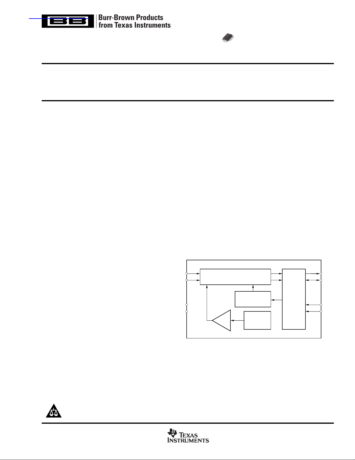
IN+
IN–
DD
2nd-Order
∆∑ Modulator
Buffer
RC Oscillator
20MHz
Reference
Voltage
2.5V
Interface
Circuit
MDAT
MCLK
M0
M1
Please be aware that an important notice concerning availability, standard warranty, and use in critical applications of
Texas Instruments semiconductor products and disclaimers thereto appears at the end of this data sheet.
PRODUCTION DATA information is current as of publication date.
Products conform to specifications per the terms of Texas Instruments
standard warranty. Production processing does not necessarily include
testing of all parameters.
Copyright © 2002, Texas Instruments Incorporated
www.ti.com
Page 2
ABSOLUTE MAXIMUM RATINGS
Over operating free-air temperature (unless otherwise noted)
(1)
ELECTROSTATIC
DISCHARGE SENSITIVITY
Supply Voltage, GND to VDD................................................. –0.3V to 6V
Analog Input Voltage Range ......................... GND – 0.4V to VDD + 0.3V
Digital Input Voltage Range .......................... GND – 0.3V to V
Power Dissipation ............................................................................ 0.25W
Operating Virtual Junction Temperature Range, T
Operating Free-Air Temperature Range, T
Storage Temperature Range, T
Lead Temperature 1.6mm (1/16") from Case for 10s .................. +260°C
NOTE: (1) Stresses beyond those listed under the Absolute Maximum Ratings
may cause permanent damage to the device. These are stress ratings only,
and functional operation of the device at these or any other conditions beyond
those indicated under the Recommended Operating Conditions is not implied.
Exposure to absolute-maximum-rated conditions for extended periods may
affect device reliability.
................................–65°C to +150°C
STG
........ –40°C to +150°C
J
....................–40°C to +85°C
A
+ 0.3V
DD
PACKAGE/ORDERING INFORMATION
MAXIMUM
INTEGRAL SPECIFIED
PRODUCT ERROR (LSB) GAIN ERROR (%) PACKAGE-LEAD DESIGNATOR
ADS1202 12 ±2 TSSOP-8 PW –40°C to +85°C ADS1202I ADS1202IPWT Tape and Reel, 250
ADS1202
NOTE: (1) For the most current specifications and package information, refer to our web site at www.ti.com.
LINEARITY MAXIMUM PACKAGE TEMPERATURE PACKAGE ORDERING TRANSPORT
"" """"
This integrated circuit can be damaged by ESD. Texas Instruments recommends that all integrated circuits be handled with
appropriate precautions. Failure to observe proper handling
and installation procedures can cause damage.
ESD damage can range from subtle performance degradation to complete device failure. Precision integrated circuits
may be more susceptible to damage because very small
parametric changes could cause the device not to meet its
published specifications.
(1)
RANGE MARKING NUMBER MEDIA, QUANTITY
ADS1202IPWR Tape and Reel, 2000
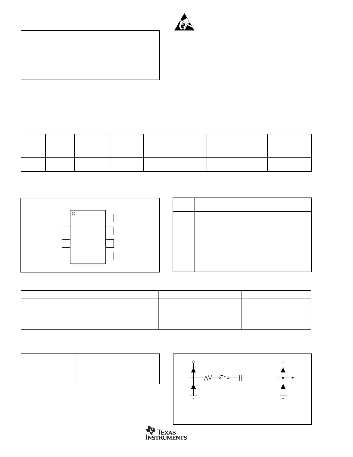
PIN CONFIGURATION
Top View TSSOP
1
M0
2
V
IN+
V
IN–
M1
ADS1202
3
4
8
V
DD
7
MCLK
6
MDAT
5
GND
PIN DESCRIPTIONS
PIN
NUMBER NAME DESCRIPTION
1 MO Mode Input
2V
3V
4 M1 Mode Input
5 GND Power Supply Ground
6 MDAT Modulator Data Output
7 MCLK Modulator Clock Input or Output
8VDDPower Supply, +5V Nominal
+ Analog Input: Noninverting Input
IN
– Analog Input: Inverting Input
IN
RECOMMENDED OPERATING CONDITIONS
PARAMETER MIN NOM MAX UNIT
Supply Voltage, V
Analog Input Voltage, V
Operating Common-Mode Signal, V
External Clock
Operating Junction Temperature Range –40 105 °C
NOTE: (1) With reduced accuracy, minimum clock can go up to 500kHz.
DD
IN
(1)
CM
DISSIPATION RATING
T
< 25°C FACTOR TA = 70°CTA = 85°C
A
PACKAGE RATING T
TSSOP-8 483.6mW 3.868mW/°C 309.5mW 251.4mW
NOTE: (1) This is the inverse of the traditional junction-to-ambient thermal
resistance (R
informational purposes only.
POWER ABOVE POWER POWER
). Thermal resistances are not production tested and are for
θ
JA
DERATING
= 25°C
A
(1)
RATING RATING
4.75 5.0 5.25 V
–250 +250 mV
05V
81012MHz
EQUIVALENT INPUT CIRCUIT
AV
DD
RON = 350Ω
A
IN
AGND
Diode Turn on Voltage: 0.35V
Equivalent Analog Input Circuit
C
(SAMPLE)
= 5pF
BV
DD
D
IN
BGND
Equivalent Digital Input Circuit
2
www.ti.com
ADS1202
SBAS275
Page 3

ELECTRICAL CHARACTERISTICS
Over recommended operating free-air temperature range at –40°C to +85°C, VDD = 5V, +In = –250mV to 250mV, –In = 0V, and MCLK = 10MHz, unless otherwise noted.
ADS1202IPW
PARAMETER CONDITIONS MIN TYP
(1)
RESOLUTION 16 Bits
DC ACCURACY
Integral Nonlinearity INL ±3 ±12 LSB
Differential Linearity
Input Offset V
Input Offset Drift TCV
Gain Error G
Gain Error Drift TCG
Power-Supply Rejection Ratio PSRR 4.75V < V
(1)
DNL ±1 LSB
OS
OS
ERR
ERR
< 5.25V 80 dB
DD
0.005 0.018 %
±300 ±1000 µV
28µV/°C
±0.25 ±2%
20 ppm/°C
ANALOG INPUT
Full-Scale Range FSR +In – (–In) ±320 mV
Operating Common-Mode Signal
(2)
–0.1 5 V
Input Capacitance Common-Mode 3 pF
Input Leakage Current ±1nA
Differential Input Resistance Equivalent 28 kΩ
Differential Input Capacitance 5pF
Common-Mode Rejection Ratio
(2)
CMRR At DC 90 dB
V
= ±1.25Vp-p at 50kHz 85 dB
IN
INTERNAL VOLTAGE REFERENCE
Reference Voltage V
Initial Accuracy Scale to 320mV ±2+-+ %
Reference Temperature Drift dV
PSRR 80 dB
OUT
/dT ±20 ppm/°C
OUT
Scale to 320mV 2.450 2.5 2.550 V
Startup Time 0.1 ms
INTERNAL CLOCK FOR MODES, 0, 1, AND 2
Clock Frequency 8 10 12 MHz
EXTERNAL CLOCK FOR MODE 3
Clock Frequency 16 20 24 MHz
AC ACCURACY
Signal-to-Noise Ratio + Distortion SINAD V
Signal-to-Noise Ratio SNR V
Total Harmonic Distortion THD V
Spurious Free Dynamic Range SFDR V
= ±250mVp-p at 5kHz 70 dB
IN
= ±250mVp-p at 5kHz 67 70.5 dB
IN
= ±250mVp-p at 5kHz –84 dB
IN
= ±250mVp-p at 5kHz 84 dB
IN
DIGITAL INPUT
Logic Family TTL with Schmitt Trigger
High-Level Input Voltage V
Low-Level Input Voltage V
High-Level Input Current I
Low-Level Input Current I
Input Capacitance C
IH
IL
IH
IL
J
VI = V
DD
VI = GND –2.5 0.005 µA
2.6 VDD + 0.3 V
–0.3 0.8 V
0.005 2.5 µA
5pF
DIGITAL OUTPUT
High-Level Digital Output V
Low-Level Digital Output V
Output Capacitance C
Load Capacitance C
OH
OL
O
L
VDD = 4.5V, IO = –5mA 4.6 V
V
= 4.5V, IO = –15mA 3.9 V
DD
VDD = 4.5V, IO = 5mA 0.4 V
V
= 4.5V, IO = 15mA 1.1 V
DD
5pF
POWER SUPPLY
Supply Voltage V
Operating Supply Current I
DD
CC
Power Dissipation V
Mode 0 6 7.5 mA
Mode 3 8 9.5 mA
= 5V, Mode 0 30 37.5 mW
DD
V
= 5V, Mode 3 40 47.5 mW
DD
4.5 5 5.5 V
OPERATING TEMPERATURE –40 +85 °C
NOTES: (1) All typical values are at T
line through the transfer curve for V
typical information parameter not tested.
= +25°C. (2) Ensured by design. (3) Integral nonlinearity is defined as one-half the peak-to-peak deviation of the best fit
A
+ = –250mV to +250mV, expressed either as the number of LSBs or as a percent of measured input range (500mV). (4) Only
IN
MAX UNITS
30 pF
ADS1202
SBAS275
www.ti.com
3
Page 4
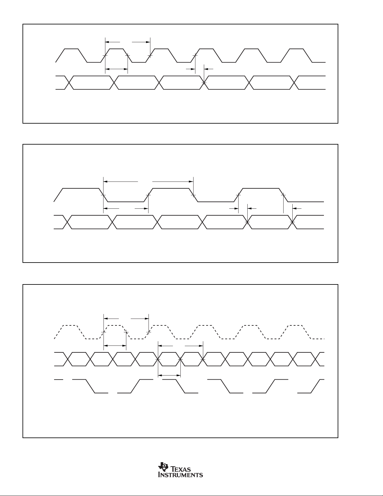
TIMING DIAGRAMS
MCLK
MDAT
DIAGRAM 1: Mode 0 Operation.
MCLK
t
C1
t
W1
t
C2
t
D1
MDAT
DIAGRAM 2: Mode 1 Operation.
MCLK
MDAT
t
W2
t
C1
t
w1
t
C3
t
w3
t
D2
t
D3
10 1100
DIAGRAM 3: Mode 2 Operation.
4
www.ti.com
ADS1202
SBAS275
Page 5
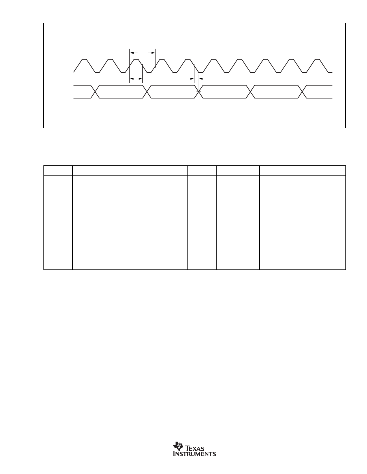
TIMING DIAGRAMS (Cont.)
t
C4
MCLK
t
w4
t
D4
MDAT
DIAGRAM 4: Mode 3 Operation.
TIMING CHARACTERISTICS
over recommended operating free-air temperature range –40°C to +85°C, VDD = 5V, and MCLK = 10MHz, unless otherwise noted.
SPEC DESCRIPTION MODE MIN MAX UNITS
t
C1
t
W1
t
D1
t
C2
t
W2
t
D2
t
D3
t
C3
t
W3
t
C4
t
W4
t
D4
t
R1
t
F1
NOTE: All input signals are specified with t
Clock Period 0 90 110 ns
Clock HIGH Time 0 tC1/2 – 5t
/2 + 5 ns
C1
Data delay after rising edge of clock 0 tC1/4 – 10 tC1/4 + 10 ns
Clock Period 1 180 220 ns
Clock HIGH Time 1 tC2/2 – 5t
/2 + 5 ns
C2
Data delay after rising edge of clock 1 tC2/4 – 10 tC2/4 + 10 ns
Data delay after falling edge of clock 1 tC2/4 – 10 tC2/4 + 10 ns
Clock Period 2 90 110 ns
Clock HIGH Time 2 tC3/2 – 5t
/2 + 5 ns
C3
Clock Period 3 45 55 ns
Clock HIGH Time 3 10 tC4 – 10 ns
Data delay after falling edge of clock 3 0 10 ns
Rise Time of Clock 3 0 10 ns
Fall Time of Clock 3 0 10 ns
= tF = 5ns (10% to 90% of VDD) and timed from a voltage level of (VIL + VIH)/2. See timing diagrams 1 thru 4.
R
ADS1202
SBAS275
www.ti.com
5
Page 6
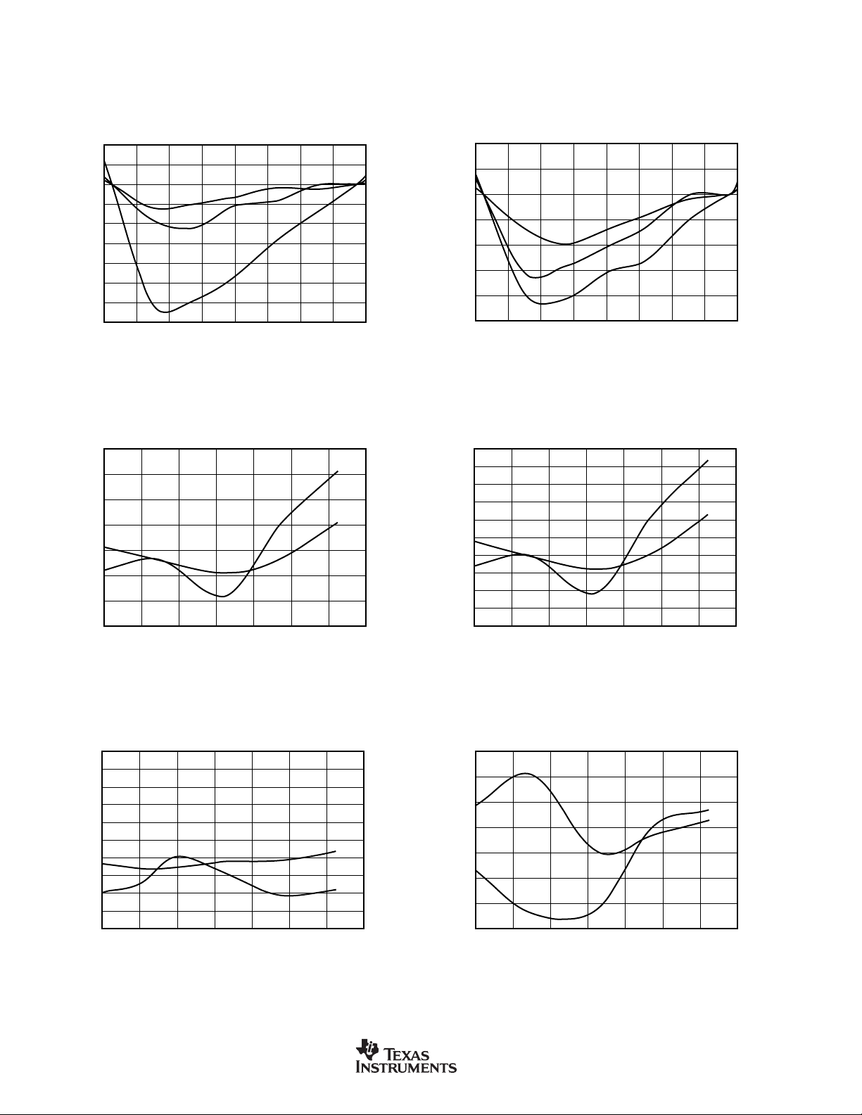
TYPICAL CHARACTERISTICS
VDD = 5V, +In = –250mV to 250mV, –In = 0V, and MCLK = 10MHz, unless otherwise noted.
INTEGRAL NONLINEARITY vs INPUT SIGNAL (Mode 0)
2
1
0
–1
–2
–3
INL (LSB)
–4
–5
–6
–7
INTEGRAL NONLINEARITY vs TEMPERATURE
7
6
5
4
3
INL (LSB)
2
1
0
–40 –20 200408060 100
25°C
–40°C
+85°C
0–320 –240 –80–160 80 240160 320
Differential Input Voltage (mV)
Mode 0
Mode 3
Temperature (°C)
INTEGRAL NONLINEARITY vs INPUT SIGNAL (Mode 3)
2
1
0
–1
–2
INL (LSB)
–3
–4
–5
0.010
0.009
0.008
0.007
0.006
0.005
INL (%)
0.004
0.003
0.002
0.001
INTEGRAL NONLINEARITY vs TEMPERATURE
0
–40 –20 200408060 100
25°C
–40°C
0–320 –240 –80–160 80 240160 320
Differential Input Voltage (mV)
Mode 0
Mode 3
Temperature (°C)
+85°C
300
200
100
0
–100
–200
–300
Offset (µV)
–400
–500
–600
–700
–40 –20 200408060 100
6
OFFSET vs TEMPERATURE
Mode 3
Mode 0
Temperature (°C)
www.ti.com
0.14
0.12
0.10
0.08
0.06
Gain (%)
0.04
0.02
0
–40 –20 200408060 100
GAIN vs TEMPERATURE
Mode 3
Mode 0
Temperature (°C)
ADS1202
SBAS275
Page 7
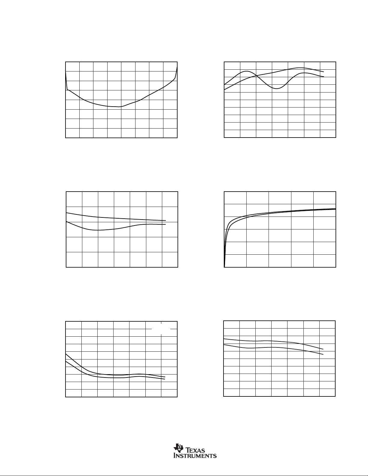
TYPICAL CHARACTERISTICS (Cont.)
SIGNAL-TO-NOISE RATIO vs TEMPERATURE
–40 –20 200408060 100
Temperature (°C)
SNR (dB)
71.0
70.8
70.6
70.4
70.2
70.0
69.8
69.6
69.4
69.2
69.0
Mode 0
Mode 3
EFFECTIVE NUMBER OF BITS
vs DECIMATION RATIO
0 400 800 1200 1600 2000
Decimation Ratio (OSR)
ENOB
16
14
12
10
8
6
4
Sinc
3
Filter
Sinc
2
Filter
VDD = 5V, +In = –250mV to 250mV, –In = 0V, and MCLK = 10MHz, unless otherwise noted.
80
70
60
50
40
30
RMS Noise (µV)
20
10
0
–320 –240 –80–160 0 24016080 320
71.0
70.6
70.2
RMS NOISE vs INPUT VOLTAGE LEVEL
Differential Input Voltage (mV)
SIGNAL-TO-NOISE + DISTORTION
vs TEMPERATURE
Mode 3
69.8
SINAD (dB)
69.4
69.0
–40 –20 200408060 100
Temperature (°C)
SPURIOUS-FREE DYNAMIC RANGE
AND TOTAL HARMOINIC DISTORTION
95
93
91
89
87
85
83
SFDR (dB)
81
79
77
75
–40 –20 200408060 100
ADS1202
SBAS275
vs TEMPERATURE (Mode 0)
SFDR
THD
Temperature (°C)
Mode 0
0.5Vp-p
5kHz
–95
–93
–91
–89
–87
–85
THD (dB)
–83
–81
–79
–77
–75
www.ti.com
SPURIOUS-FREE DYNAMIC RANGE
AND TOTAL HARMOINIC DISTORTION
95
93
91
89
87
85
83
SFDR (dB)
81
79
77
75
–40 –20 200408060 100
vs TEMPERATURE (Mode 3)
SFDR
THD
Temperature (°C)
–95
–93
–91
–89
–87
–85
–83
–81
–79
–77
–75
THD (dB)
7
Page 8

TYPICAL CHARACTERISTICS (Cont.)
SPURIOUS-FREE DYNAMIC RANGE
AND TOTAL HARMOINIC DISTORTION
vs INPUT FREQUENCY (Mode 3)
110
Input Frequency (kHz)
SFDR
THD
SFDR (dB)
THD (dB)
110
100
90
80
70
60
50
–110
–100
–90
–80
–70
–60
–50
OSR = 256
Sinc
3
Filter
VDD = 5V, +In = –250mV to 250mV, –In = 0V, and MCLK = 10MHz, unless otherwise noted.
SPURIOUS-FREE DYNAMIC RANGE
AND TOTAL HARMOINIC DISTORTION
110
vs INPUT FREQUENCY (Mode 0)
–110
100
90
80
SFDR (dB)
70
60
50
110
0
–20
–40
–60
–80
Magnitude (dB)
–100
SFDR
OSR = 256
3
Sinc
Filter
THD
Input Frequency (kHz)
FREQUENCY SPECTRUM
(4096 Point FFT, f
= 1kHz, 0.5Vp-p)
IN
Mode 0
–100
–90
–80
–70
–60
–50
THD (dB)
0
–20
–40
–60
–80
Magnitude (dB)
–100
FREQUENCY SPECTRUM
(4096 Point FFT, f
= 5kHz, 0.5Vp-p)
IN
Mode 0
–120
–140
10.5
10.2
9.9
9.6
MCLK (MHz)
9.3
9.0
8
–40 –20 0 20 40 60 80 100 120
CLOCK FREQUENCY vs TEMPERATURE
802 641014161812 20
Frequency (kHz)
Temperature (°C)
www.ti.com
–120
–140
100
95
90
85
80
75
70
CMRR (dB)
65
60
55
50
1 10 100
802 641014161812 20
Frequency (kHz)
COMMON-MODE REJECTION RATIO
vs FREQUENCY
Frequency of Power Supply (Hz)
ADS1202
SBAS275
Page 9
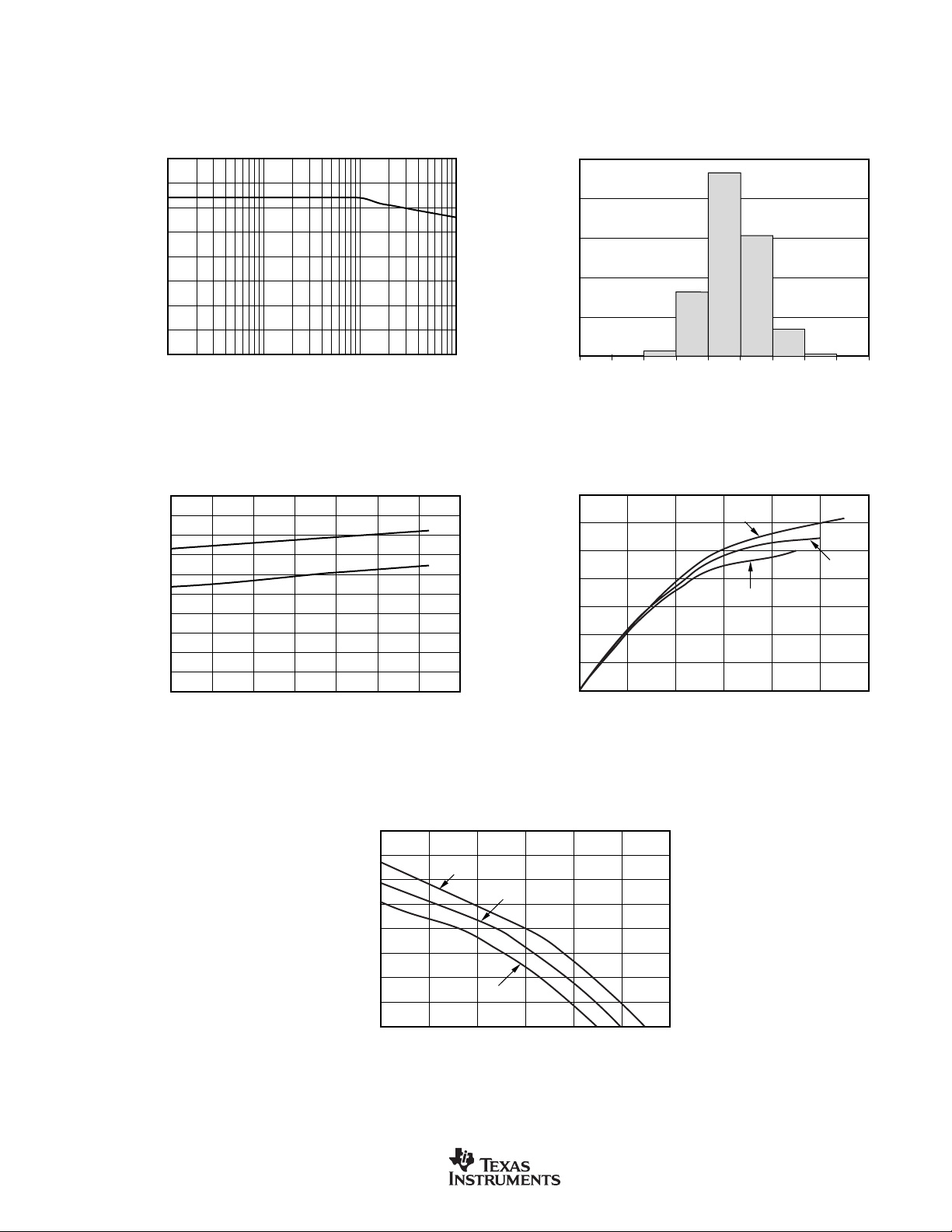
TYPICAL CHARACTERISTICS (Cont.)
2000
1800
1600
1400
1200
1000
800
600
400
200
0
HISTOGRAM OF OUTPUT DATA
ppm of FS
–1114
–1053
–992
–931
–870
–809
–748
–687
–626
Number of Occurrences
MCLK AND MDAT
TYPICAL SINK CURRENT
3012 456
Output Voltage V
OL
(V)
Output Current I
OL
(mA)
70
60
50
40
30
20
10
0
5.5V
5V
4.5V
k
VDD = 5V, +In = –250mV to 250mV, –In = 0V, and MCLK = 10MHz, unless otherwise noted.
POWER-SUPPLY REJECTION RATIO
90
85
80
75
70
PSRR (dB)
65
60
55
50
100 1k 10k 100
POWER-SUPPLY CURRENT vs TEMPERATURE
10
9
8
7
6
5
4
Current (mA)
3
2
1
0
–40 –20 200408060 100
vs FREQUENCY
Frequency of Power Supply (Hz)
Mode 0
Mode 3
Temperature (°C)
ADS1202
SBAS275
80
70
60
(mA)
50
OH
40
30
20
Output Current I
10
0
MCLK AND MDAT
TYPICAL SOURCE CURRENT
5.5V
5V
4.5V
3012 456
Output Voltage V
(V)
OH
www.ti.com
9
Page 10

GENERAL DESCRIPTION
The ADS1202 is a single-channel, 2nd-order, CMOS analog
modulator designed for medium to high resolution conversions from DC to 39kHz with an oversampling ratio (OSR) of
256. The output of the converter (MDAT) provides a stream
of digital ones and zeros. The time average of this serial
output is proportional to the analog input voltage. The combination of an ADS1202 and a Digital Signal Processor
(DSP) that is programmed to implement a digital filter results
in a medium resolution A/D converter system. This system
allows flexibility with the digital filter design and is capable of
A/D conversion results that have a dynamic range that
exceeds 85dB with OSR = 256.
THEORY OF OPERATION
The differential analog input of the ADS1202 is implemented
with a switched capacitor circuit. This switched capacitor
circuit implements a 2nd-order modulator stage, which digitizes the input signal into a 1-bit output stream. The sample
clock (MCLK) provides the switched capacitor network and
modulator clock signal for the A/D conversion process, as
well as the output data-framing clock. The clock source can
be internal as well as external. Different frequencies for this
clock allow for a variety of solutions and signal bandwidths
(however, this can only be utilized in mode 3). The analog
input signal is continuously sampled by the modulator and
compared to an internal voltage reference. A digital stream,
which accurately represents the analog input voltage over
time, appears at the output of the converter.
+5V+5V
M
27Ω
27Ω
0.1µF0.1µF
10nF
M0
V
V
M1
IN
IN
ADS1202
+
–
V
MCLK
MDAT
GND
DD
0.1µF
FIGURE 1. Connection Diagram for the ADS1202 Delta-Sigma Modulator Including DSP.
V
DDO
SPICLK
SPISIMO
V
SSO
DSP
10
www.ti.com
ADS1202
SBAS275
Page 11

ANALOG INPUT STAGE
Analog Input
The input design topology of the ADS1202 is based on a fully
differential switched-capacitor architecture. This input stage
provides the mechanism to achieve low system noise, high
common-mode rejection (90dB), and excellent power-supply
rejection. The input impedance of the analog input is dependant on the input capacitor and modulator clock frequency
(MCLK), which is also the sampling frequency of the modulator. Figure 2 shows the basic input structure of the ADS1202.
The relationship between the input impedance of the ADS1202
and the modulator clock frequency is:
A
Ω
=
(
)
IN
The input impedance becomes a consideration in designs
where the source impedance of the input signal is HIGH. In
this case, it is possible for a portion of the signal to be lost
across this external source impedance. The importance of this
effect depends on the desired system performance. There are
two restrictions on the analog input signal to the ADS1202.
Under no conditions should the current into or out of the
analog inputs exceed 10mA. The absolute input voltage range
must stay in the range GND – 0.4V to V
the inputs exceed these limits, the input protection diodes on
the front end of the converter will begin to turn on. In addition,
12
f MHz
•107
MCLK
()
+ 0.3V. If either of
DD
(1)
the linearity of the device is ensured only when the analog
voltage applied to either input resides within the range defined
by –320mV and +320mV.
Modulator
The modulator sampling frequency (CLK) can be operated
over a range of a few MHz to 12MHz in mode 3. The
frequency of MCLK can be decreased to adjust for the clock
requirements of the application. The external MCLK must
have double the modulator frequency.
The modulator topology is fundamentally a 2nd-order, chargebalancing A/D converter, as the one conceptualized in Figure 3.
The analog input voltage and the output of the 1-bit Digital-toAnalog Converter (DAC) are differentiated, providing an analog
voltage at X
to their individual integrators. The output of these integrators
progress in a negative or positive direction. When the value of
the signal at X
output of the comparator switches from negative to positive, or
positive to negative, depending on its original state. When the
output value of the comparator switches from HIGH to LOW or
vice versa, the 1-bit DAC responds on the next clock pulse by
changing its analog output voltage at X
to progress in the opposite direction. The feedback of the
modulator to the front end of the integrators forces the value of
the integrator output to track the average of the input.
and X3. The voltage at X2 and X3 are presented
2
equals the comparator reference voltage, the
4
, causing the integrators
6
AIN+
Switching Frequency
= CLK
AIN–
FIGURE 2. Input Impedance of the ADS1202.
X
X(t)
f
S
2
Integrator 1
1.5pF
1.5pF
R
SW
350kΩ (typ)
R
SW
350kΩ (typ)
X
3
V
Integrator 2
CM
C
INT
7pF (typ)
C
INT
7pF (typ)
X
V
REF
4
High
Impedance
> 1GΩ
High
Impedance
> 1GΩ
f
CLK
Comparator
DATA
FIGURE 3. Block Diagram of the 2nd-Order Modulator.
ADS1202
SBAS275
www.ti.com
X
6
D/A Converter
11
Page 12
DIGITAL OUTPUT
The timing diagram for the ADS1202 data retrieval is shown
in the Timing Diagrams. When an external clock is applied to
MCLK, it is used as a system clock by the ADS1202, as well
as a framing clock for data out (this procedure, however, can
only be utilized in mode 3). The modulator output data, which
is a serial stream, is available on the MDAT pin. Typically,
MDAT is read on the falling edge of MCLK.
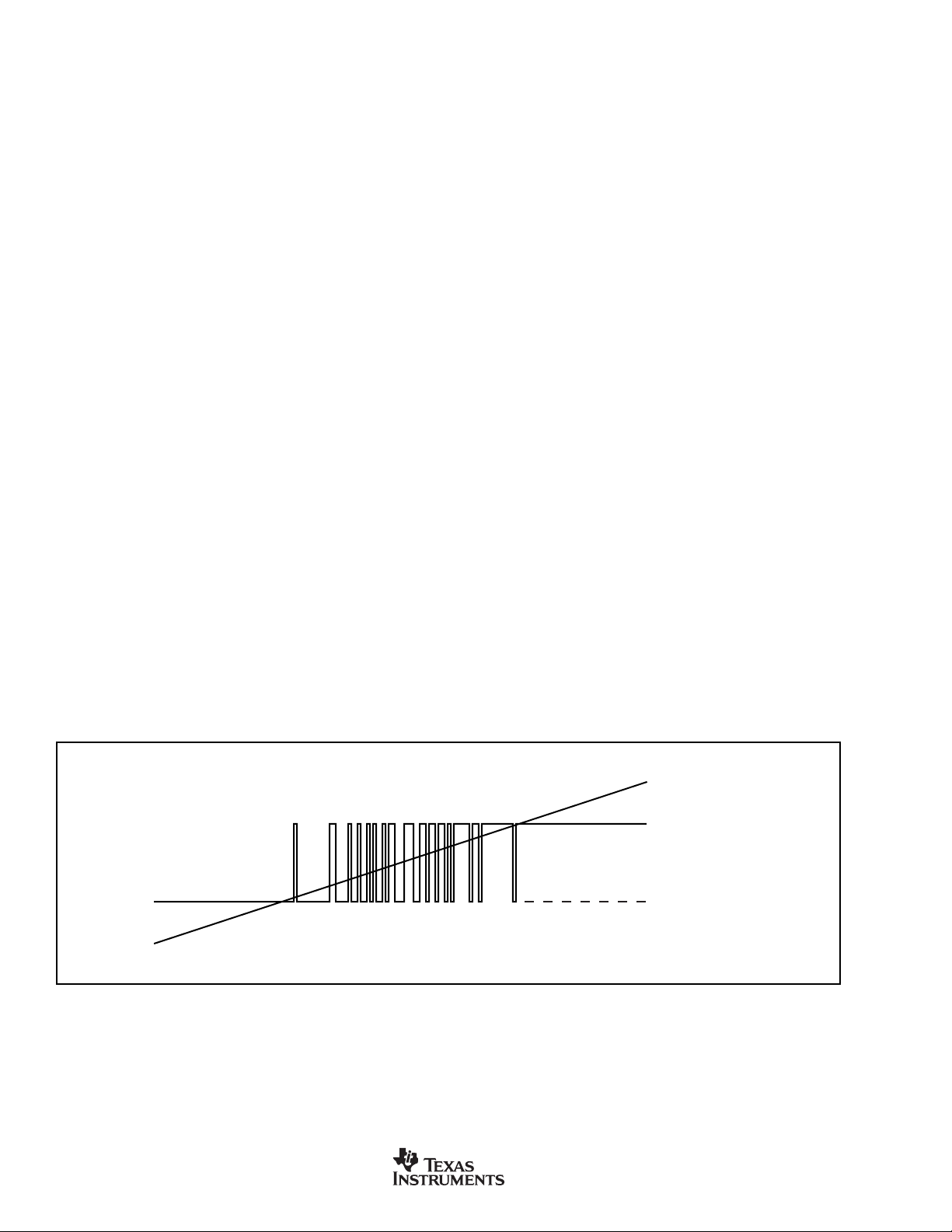
An input differential signal of 0V will ideally produce a stream
of ones and zeros that are HIGH 50% of the time and LOW
50% of the time. A differential input of 256mV will produce a
stream of ones and zeros that are HIGH 80% of the time. A
differential input of –256mV will produce a stream of ones
and zeros that are HIGH 20% of the time. The input voltage
versus the output modulator signal is shown in Figure 4.
DIGITAL INTERFACE
INTRODUCTION
The analog signal that is connected to the input of the delta-sigma
modulator is converted using the clock signal (CLK) applied to the
modulator. The result of the conversion, or modulation, is the
output signal DATA from the delta-sigma modulator.
In most applications where direct connection is realized
between delta-sigma modulator and DSP or uC, two standard signals are provided. The MDAT and MCLK signals
provide the easiest means of connection. If it is required to
reduce the number of connection lines, having two signals is
sometimes not an optimal solution.
The receiver, DSP, or other control circuit must sample the
output data signal from the modulator at the precise sampling
instant. To do this, sampling a clock signal at the receiver is
needed in order to synchronize with the clock signal at the
transmitter. The delta-sigma modulator clock signal, receiver,
filter, and clock must be synchronized. Three general meth-
ods can be used to obtain this synchronization. The first
method has the delta-sigma modulator and the filter receive
the clock signal from the master clock. The second method
has the delta-sigma modulator transmit the clock signal
together with the data signal. The third method has the filter
derivate the clock signal from the received waveform itself.
An ideal solution is a delta-sigma modulator with a flexible
interface, such as the ADS1202, which can provide flexible
output format on the output lines MCLK and MDAT, thus
covering different modes of operation. The signal type that
can be provided is selected with control signals M0 and M1.
FLEXIBLE DELTA-SIGMA INTERFACE
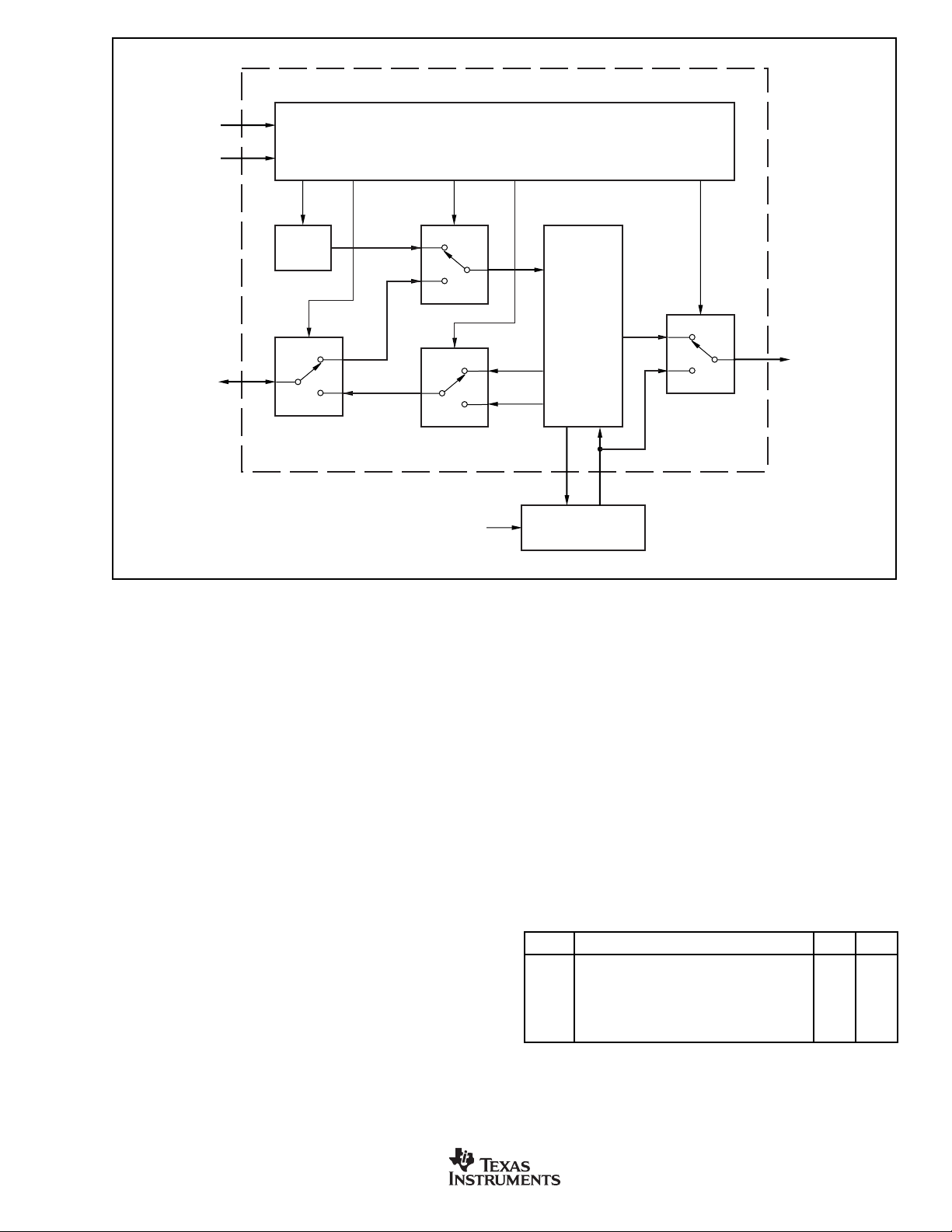
Figure 5 illustrates the flexible interface of the ADS1202
delta-sigma converter. The control signals M0 and M1 are
entered in the decoder that decodes the input code and
selects the desired mode of operation. Five output signals
from the decoder control the RC oscillator, multiplexer MUX1,
multiplexer MUX2, multiplexer MUX3, and multiplexer MUX4.
MUX1 is controlled by the decoder signal. When the internal
RC oscillator is used, the control signal from the decoder
enables the RC oscillator. At the same time, MUX1 uses the
INTCLK signal as a source for the output signal from MUX1,
which is entering the code generator. If the external clock is
used, the control signal from the decoder disables the internal RC oscillator and the control signal from the decoder, and
positions MUX1 so that EXTCLK provides the output signal
from MUX1 as the input in the code generator.
MUX2 selects the output clock, OCLK. The control signal
coming from the decoder controls the output clock. Two
signals come from the code generator as a half clock frequency, CLK/2, and as a quarter clock frequency, CLK/4,
and provide MUX2 with the input signal. The control signal
will select two different output modes on the OCLK signal as
half clock or quarter clock.
Modulator Output
Analog Input
FIGURE 4. Analog Input Versus Modulator Output of the ADS1201.
12
www.ti.com
+FS (Analog Input)
–FS (Analog Input)
ADS1202
SBAS275
Page 13
M0
M1
Interface Circuit
Decoder
MUX1
MUX2
AIN
MCLK
RC
Oscillator
MUX4
INTCLK
EXTCLK
OCLK
FIGURE 5. Flexible Interface Block Diagram.
The code generator receives the clock signal from MUX1 and
generates the delta-sigma modulator clock (CLK) divided as
half clock (CLK/2) and quarter clock (CLK/4). At the same
time, the continuous data stream (DATA) coming from the
delta-sigma modulator is elaborated by the Code Generator.
Twinned binary coding (also known as split phase or Manchester coding) is implemented and then output from the code
generator to MUX3.
MUX3 selects the source of the output bit stream data,
MDAT. The control signal coming from the decoder controls
the input source of MDAT. Two signals are coming in to the
MUX3, one directly from the delta-sigma modulator and the
other from the code generator. The control signal from the
decoder can select two different output modes on the signal
MDAT: bit stream from a delta-sigma modulator or twinned
binary coding of the same signal.
The last control signal from the decoder controls MUX4.
MUX2 selects the input or output clock, the MCLK signal.
The control signal coming from the decoder controls the
direction of the clock. One signal entering MUX4 from MUX2
comes as a clock signal OCLK. Another signal leaves MUX4
and provides an input to MUX1 as an external clock, EXTCLK.
Code
Generator
CLK/2
CLK/4
CLK DATA
∆∑
Modulator
MUX3
MDAT
The control signal from the decoder can select two different
modes on MCLK, one as an output of the internal clock signal
and another as the input for the external clock signal.
As a function of two control signals (M0 and M1), the decoder
circuit, using five control signals, will set multiplexers in order
to obtain the desired mode of operation.
DIFFERENT MODES OF OPERATION
Figure 5 presents mode selectors (input signals M0 and M1)
that enter the flexible interface circuit and decoder that
decodes the input code, and select the desired mode of
operation. With two control lines it is possible to select four
different modes of operation mode 0, mode 1, mode 2, and
mode 3, which are shown in Table I.
MODE DEFINITION M1 MO
0 Internal Clock, Synchronous Data Output LOW LOW
1 Internal Clock, Synchronous Data Output, LOW HIGH
Half Output Clock Frequency
2 Internal Clock, Manchester Coded Data Output HIGH LOW
3 External Clock, Synchronous Data Output HIGH HIGH
TABLE I. Mode Definition and Description.
ADS1202
SBAS275
www.ti.com
13
Page 14

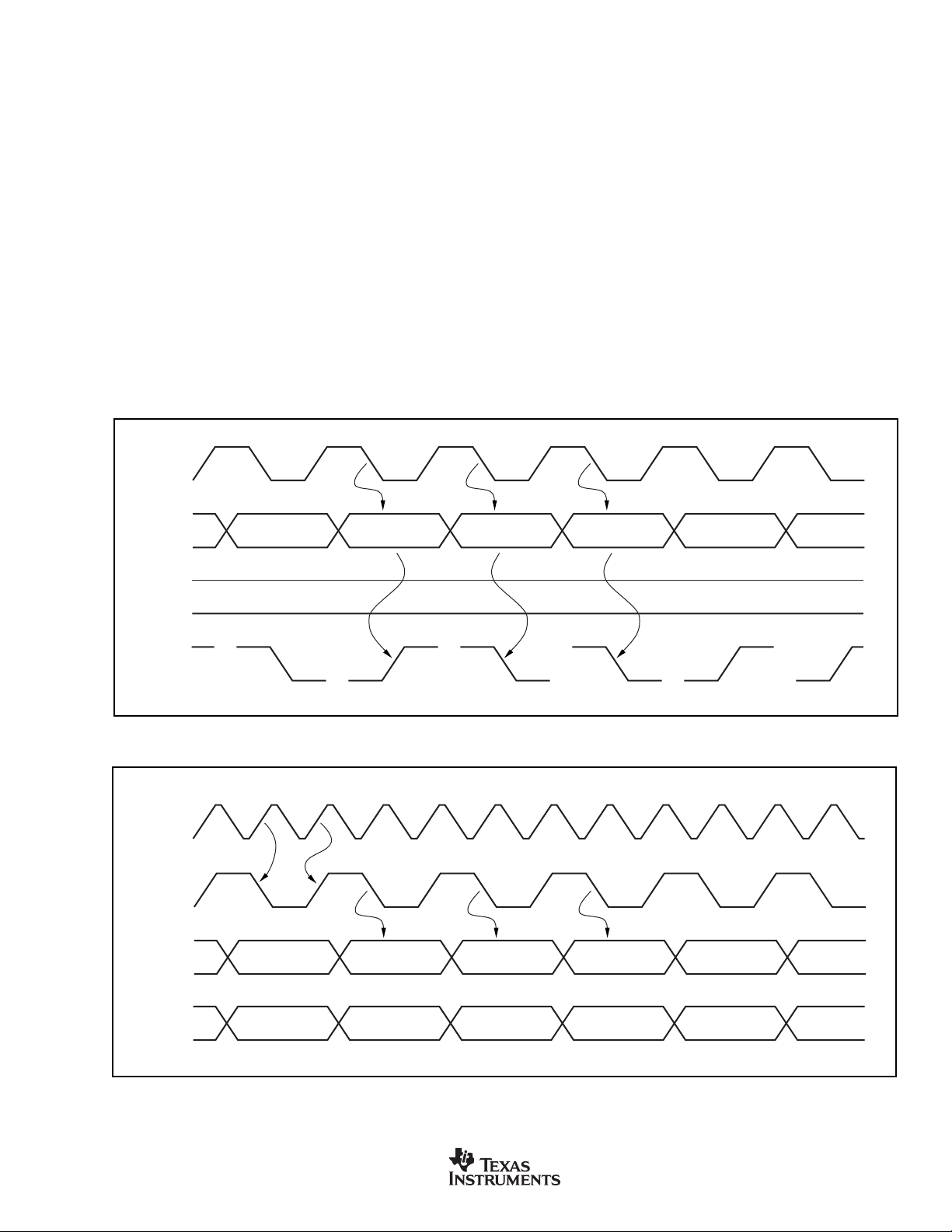
Mode 0
In mode 0 both input signals, M0 and M1, are LOW. The
control signal coming from the decoder enables the internal
RC oscillator that provides the clock signal INTCLK as an
input to MUX1. The control signal coming from the decoder
also positions MUX1 so that the output signal, which is an
input signal for the code generator, is INTCLK. Another
control signal from the decoder circuit positions MUX3 so
that the source for the output signal MDAT is the signal
arriving directly from the delta-sigma modulator, DATA. MUX2
is positioned for the mode controlled by the signal coming
from the decoder so output signal OCLK is CLK/2. The signal
timings for mode 0 operation are presented in Figure 6. In
this mode, DSP or µC read MDAT data on every rising edge
of the MCLK output clock.
CLK
Mode 1
In mode 1, the input signal M0 is HIGH and M1 is LOW (see
Table I). The first control signal coming from the decoder
enables the internal RC oscillator that provides clock signal
INTCLK as an input to MUX1. The second control signal
coming from the decoder positions MUX1 so that the output
signal that is the input signal to the code generator is
INTCLK. The output signal from the delta-sigma modulator,
DATA, is also the MDAT signal coming from the modulator
because the control signal from the decoder positions MUX3
for that operation. MUX2 is positioned for the mode controlled by the control signal coming from the decoder with an
OCLK of CLK/2. Output clock signal MCLK comes through
MUX4 from MUX2 as OCLK or CLK/2. The signal timings for
mode 1 operation are presented in Figure 7. In this mode,
DSP or µC read data on every edge, rising and falling, of the
output clock.
DATA
MCLK
MDAT
FIGURE 6. Signal Timing in Mode 0.
CLK
DATA
MCLK
MDAT
FIGURE 7. Signal Timing in Mode 1.
14
www.ti.com
ADS1202
SBAS275
Page 15
Mode 2
In mode 2, M0 is low and M1 is HIGH (see Table I). The control
signal coming from the decoder enables the internal RC oscillator that provides the clock signal INTCLK as an input to MUX1.
Another control signal coming from the decoder positions MUX1
so that the output signal that is the input signal to the code
generator is INTCLK. The output signal MDAT comes from the
code generator because the control signal from the decoder
positions MUX3 for that operation. The DATA signal coming
from the delta-sigma modulator enters the code generator,
where it combines with the clock signal, and twinned binary
coding is implemented as split phase or Manchester coding,
providing the output signal for MUX3. The MCLK output clock
is not active, as multiplexers MUX2 and MUX4 are positioned
for this mode controlled by the control signals coming from the
decoder. The signals timings for mode 2 operation are presented in Figure 8. In this mode, DSP or µC need to derive the
clock signal from the received waveform itself. Different clock
recovery networks can be implemented.
CLK
Mode 3
mode 3 is similar to mode 0; the only difference is that an
external clock (EXTCLK) is provided. In mode 3, both input
signals M0 and M1 are HIGH (see Table I). The control
signal coming from the decoder disables the internal RC
oscillator. The input signal EXTCLK provides the clock
signal as an input to MUX1. The control signal coming from
the decoder positions MUX1 so that the output signal that
is the input signal to the code generator is EXTCLK. The
output signal MDAT is the DATA signal coming directly from
the delta-sigma modulator because the control signal from
the decoder positions MUX3 for that operation. The signal
timings for mode 3 operation are presented in Figure 9. In
this mode, DSP or µC read data on every falling edge of the
input clock.
DATA
MCLK
MDAT
FIGURE 8. Signal Timing in Mode 2.
MCLK
CLK
DATA
MDAT
FIGURE 9. Signal Timing in Mode 3.
ADS1202
SBAS275
www.ti.com
15
Page 16
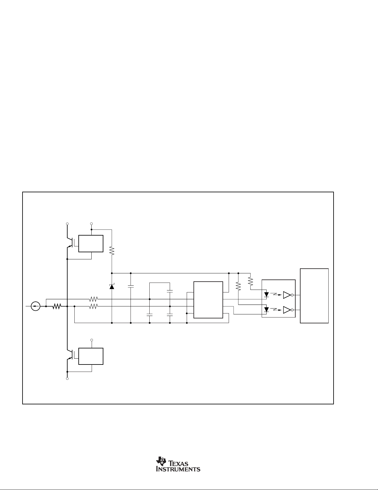
APPLICATIONS
Mode 0 operation in a typical application is shown in Figure
10. Measurement of the motor phase current is done via the
shunt resistor. For better performance, both signals are
filtered. R
signal, R
C
in combination with R2 and R3 filter the common-mode
4
input noise. In this configuration, the shunt resistor is connected via three wires with the ADS1202.
The power supply is taken from the upper gate driver power
supply. A decoupling capacitor of 0.1µF is recommended for
filtering the power supply. If better filtering is required, an
additional 1µF to 10µF capacitor can be added.
The control lines M0 and M1 are both LOW while the part is
operating in mode 0. Two output signals, MCLK and MDAT,
are connected directly to the optocoupler. The optocoupler
can be connected to transfer a direct or inverse signal
because the output stage has the capacity to source and sink
the same current. The discharge resistor is not needed in
parallel with optocoupler diodes because the output driver
has the capacity to keep the LED diode out of the charge.
and C2 filter noise on the noninverting input
2
and C3 filter noise on the inverting input signal, and
3
The DSP can be directly connected at the output of two
channels of the optocoupler, C28x or C24x. In this configuration, the signals arriving at C28x or C24x are standard
delta-sigma modulator signals and are connected directly to
the SPICLK and SPISIMO pins. Being a delta-sigma converter, there is no need to have word synch on the serial
data, so SPI is ideal for connection. McBSP would work as
well in SPI mode.
When component reduction is necessary, the ADS1202 can
operate in mode 2, as shown in Figure 11. M1 is HIGH and
M0 is LOW. Only the noninverting input signal is filtered.
R
and C2 filter noise on the input signal. The inverting input
2
is directly connected to the GND pin, which is simultaneously
connected to the shunt resistor.
The output signal from the ADS1202 is Manchester coded. In
this case, only one signal is transmitted. For that reason, one
optocoupler channel is used instead of two channels, as in
the previous example of Figure 10. Another advantage of this
configuration is that the DSP will use only one line per
channel instead of two. That permits the use of smaller DSP
packages in the application.
R
SENSE
HV+
HV–
Floating
Power Supply
Gated
Drive Circuit
R
2
27Ω
R
3
27Ω
Power
Supply
Gated
Drive Circuit
R
D
5.1V
1
C28x
R
5
C
1
1
0.1µF
C
2
0.1µF
C
4
10nF
C
3
0.1µF
ADS1202
M0
+
V
IN
–
V
IN
M1
V
MCLK
MDAT
GND
R
4
DD
Optocoupler
C24x
SPICLK
SPISIMO
or
FIGURE 10. Application Diagram in Mode 0.
16
www.ti.com
ADS1202
SBAS275
Page 17

FIGURE 11. Application Diagram in Mode 2.
R
SENSE
R
2
27Ω
D
1
5.1V
R
1
C
1
0.1µF
ADS1202
C
2
0.1µF
R
4
M0
V
IN
+
V
IN
–
M1
V
DD
MCLK
MDAT
GND
HV+
HV–
Floating
Power Supply
Gated
Drive Circuit
C28x
or
C24x
Optocoupler
Gated
Drive Circuit
Power
Supply
Floating
HV+
Power Supply
Gate Drive
Circuit
R
2
27Ω
+
R
FIGURE 12. Application Diagram without Galvanical Isolation in Mode 0.
SENSE
–
C
2
0.1µF
ADS1202
M0
+
V
IN
–
V
IN
M1
V
MCLK
MDAT
GND
C28x
or
C24x
CV
DD
C
1
DD
0.1µF
SPICLK
SPISIMO
DV
DD
ADS1202
SBAS275
www.ti.com
17
Page 18

+
–
R
R
27Ω
SENSE
1
C
1
0.1µF
ADS1202
M0
V
+
IN
–
V
IN
M1
V
MCLK
MDAT
GND
DD
C
4
0.1µF
ADS1202
M0
V
+
IN
–
V
IN
M1
ADS1202
M0
V
+
IN
V
–
IN
M1
V
MCLK
MDAT
GND
V
MCLK
MDAT
GND
DD
DD
+
–
+
–
R
R
R
27Ω
SENSE
R
27Ω
SENSE
2
C
2
0.1µF
3
C
3
0.1µF
FIGURE 13. Parallel Operation of ADS1202 in Mode 3.
LAYOUT CONSIDERATIONS
POWER SUPPLIES
The ADS1202 requires only one power supply (VDD). If there
are separate analog and digital power supplies on the board,
a good design approach is to have the ADS1202 connected
to the analog power supply. Another approach to control the
noise is the use of a resistor on the power supply. The
connection can be made between the ADS1202 powersupply pins via a 10Ω resistor. The combination of this
resistor and the decoupling capacitors between the powersupply pins on the ADS1202 provide some filtering. The
analog supply that is used must be well regulated and low
noise. For designs requiring higher resolution from the
ADS1202, power-supply rejection will be a concern. The
digital power supply has high-frequency noise that can be
capacitively coupled into the analog portion of the ADS1202.
This noise can originate from switching power supplies,
microprocessors, or digital signal processors. High-frequency
noise will generally be rejected by the external digital filter at
integer multiples of MCLK. Just below and above these
frequencies, noise will alias back into the passband of the
digital filter, affecting the conversion result. Inputs to the
ADS1202, such as V
present before the power supply is on. Violating this condition could cause latch-up. If these signals are present before
the supply is on, series resistors should be used to limit the
+, VIN–, and MCLK should not be
IN
C
5
0.1µF
C28x
or
C24x
CV
DD
C
6
0.1µF
SPICLK
SPISIMO
SPISIMO
SPISIMO
DV
DD
CLK
input current. Experimentation may be the best way to
determine the appropriate connection between the ADS1202
and different power supplies.
GROUNDING
Analog and digital sections of the design must be carefully
and cleanly partitioned. Each section should have its own
ground plane with no overlap between them. Do not join the
ground planes, but connect the two with a moderate signal
trace underneath the converter. For multiple converters,
connect the two ground planes as close as possible to one
central location for all of the converters. In some cases,
experimentation may be required to find the best point to
connect the two planes together.
DECOUPLING
Good decoupling practices must be used for the ADS1202
and for all components in the design. All decoupling capacitors, specifically the 0.1µF ceramic capacitors, must be
placed as close as possible to the pin being decoupled. A
1µF and 10µF capacitor, in parallel with the 0.1µF ceramic
capacitor, must be used to decouple V
one 0.1µF ceramic capacitor must be used to decouple V
to GND, as well as for the digital supply on each digital
component.
to GND. At least
DD
DD
18
www.ti.com
ADS1202
SBAS275
Page 19

PW (R-PDSO-G**) PLASTIC SMALL-OUTLINE PACKAGE
14 PINS SHOWN
0,65
M
0,10
0,10
0,25
0,50
0,75
0,15 NOM
Gage Plane
28
9,80
9,60
24
7,90
7,70
2016
6,60
6,40
4040064/F 01/97
0,30
6,60
6,20
8
0,19
4,30
4,50
7
0,15
14
A
1
1,20 MAX
14
5,10
4,90
8
3,10
2,90
A MAX
A MIN
DIM
PINS **
0,05
4,90
5,10
Seating Plane
0°–8°
NOTES: A. All linear dimensions are in millimeters.
B. This drawing is subject to change without notice.
C. Body dimensions do not include mold flash or protrusion not to exceed 0,15.
D. Falls within JEDEC MO-153
PACKAGE DRAWING
ADS1202
SBAS275
www.ti.com
19
Page 20

MECHANICAL DATA
MTSS001C – JANUARY 1995 – REVISED FEBRUARY 1999
PW (R-PDSO-G**) PLASTIC SMALL-OUTLINE PACKAGE
14 PINS SHOWN
0,65
1,20 MAX
14
0,30
0,19
8
4,50
4,30
PINS **
7
Seating Plane
0,15
0,05
8
1
A
DIM
6,60
6,20
14
0,10
M
0,10
0,15 NOM
0°–8°
2016
Gage Plane
24
0,25
0,75
0,50
28
A MAX
A MIN
NOTES: A. All linear dimensions are in millimeters.
B. This drawing is subject to change without notice.
C. Body dimensions do not include mold flash or protrusion not to exceed 0,15.
D. Falls within JEDEC MO-153
3,10
2,90
5,10
4,90
5,10
4,90
6,60
6,40
7,90
7,70
9,80
9,60
4040064/F 01/97
POST OFFICE BOX 655303 • DALLAS, TEXAS 75265
1
Page 21

IMPORTANT NOTICE
Texas Instruments Incorporated and its subsidiaries (TI) reserve the right to make corrections, modifications,
enhancements, improvements, and other changes to its products and services at any time and to discontinue
any product or service without notice. Customers should obtain the latest relevant information before placing
orders and should verify that such information is current and complete. All products are sold subject to TI’s terms
and conditions of sale supplied at the time of order acknowledgment.
TI warrants performance of its hardware products to the specifications applicable at the time of sale in
accordance with TI’s standard warranty . Testing and other quality control techniques are used to the extent TI
deems necessary to support this warranty . Except where mandated by government requirements, testing of all
parameters of each product is not necessarily performed.
TI assumes no liability for applications assistance or customer product design. Customers are responsible for
their products and applications using TI components. T o minimize the risks associated with customer products
and applications, customers should provide adequate design and operating safeguards.
TI does not warrant or represent that any license, either express or implied, is granted under any TI patent right,
copyright, mask work right, or other TI intellectual property right relating to any combination, machine, or process
in which TI products or services are used. Information published by TI regarding third–party products or services
does not constitute a license from TI to use such products or services or a warranty or endorsement thereof.
Use of such information may require a license from a third party under the patents or other intellectual property
of the third party , or a license from TI under the patents or other intellectual property of TI.
Reproduction of information in TI data books or data sheets is permissible only if reproduction is without
alteration and is accompanied by all associated warranties, conditions, limitations, and notices. Reproduction
of this information with alteration is an unfair and deceptive business practice. TI is not responsible or liable for
such altered documentation.
Resale of TI products or services with statements different from or beyond the parameters stated by TI for that
product or service voids all express and any implied warranties for the associated TI product or service and
is an unfair and deceptive business practice. TI is not responsible or liable for any such statements.
Mailing Address:
Texas Instruments
Post Office Box 655303
Dallas, Texas 75265
Copyright 2002, Texas Instruments Incorporated
 Loading...