

查询ADS1201供应商查询ADS1201供应商
®
ADS1201
High Dynamic Range
DELTA-SIGMA MODULATOR
ADS1201
FEATURES
● 130dB DYNAMIC RANGE
● FULLY DIFFERENTIAL INPUT
● TWO-WIRE INTERFACE
● INTERNAL/EXTERNAL REFERENCE
● ON-CHIP SWITCHES FOR CALIBRATION
APPLICATIONS
● INDUSTRIAL PROCESS CONTROL
● INSTRUMENTATION
● SMART TRANSMITTERS
● PORTABLE INSTRUMENTS
● WEIGH SCALES
● PRESSURE TRANSDUCERS
AVDDAGND REF
REF
IN
DESCRIPTION
The ADS1201 is a precision, 130dB dynamic range,
delta-sigma (∆Σ) modulator operating from a single
+5V supply. The differential inputs are ideal for direct
connection to transducers or low level signals. With
the appropriate digital filter and modulator rate, the
device can be used to achieve 24-bit analog-to-digital
(A/D) conversion with no missing codes. Effective
resolution of 20 bits can be maintained with a digital
filter bandwidth of 1kHz at a modulator rate of 320kHz.
The ADS1201 is designed for use in high resolution
measurement applications including smart transmitters, industrial process control, weigh scales, chromatography, and portable instrumentation. It is available
in a 16-lead SOIC package.
OUT
V
BIAS
+2.5V
Reference
AINP
A
N
IN
International Airport Industrial Park • Mailing Address: PO Box 11400, Tucson, AZ 85734 • Street Address: 6730 S. Tucson Blvd., Tucson, AZ 85706 • Tel: (520) 746-1111
Twx: 910-952-1111 • Internet: http://www.burr-brown.com/ • Cable: BBRCORP • Telex: 066-6491 • FAX: (520) 889-1510 • Immediate Product Info: (800) 548-6132
©
1997 Burr-Brown Corporation PDS-1417C Printed in U.S.A. October, 1999
Second-Order
∆Σ
Modulator
CAL GAIN/OFFSET DGNDDV
Bias
Generator
DD
BIAS
REF
MOUT
MCLK
EN
EN

SPECIFICATIONS
At TA = +25°C, AVDD = DVDD = +5V, MCLK = 320kHz, REFEN LOW, BIASEN LOW, and external +2.5V reference, unless otherwise specified.
ADS1201U
PARAMETER CONDITIONS MIN TYP MAX UNITS
ANALOG INPUT
Absolute Input Voltage Range 0 +5 V
With V
Differential Input Voltage Range –5 +5 V
With V
Input Impedance 250
Input Capacitance 8pF
Input Leakage Current 550pA
At T
SYSTEM PERFORMANCE
Dynamic Range 10Hz Bandwidth
60Hz Bandwidth
1kHz Bandwidth
Integral Linearity Error 60Hz Bandwidth
Offset Error
Offset Drift
Gain Error
(2)
(3)
(2)
Gain Error Drift
(3)
1kHz Bandwidth
Common-Mode Rejection At DC 80 100 dB
Power Supply Rejection 80 dB
REFERENCE
Internal Reference (REF
Drift 25 ppm/°C
) 2.4 2.5 2.6 V
OUT
Noise 50 µVp-p
Load Current Source or Sink –1 1 mA
Output Impedance 2 Ω
External Reference (REF
Load Current 2.5 µA
V
Output Using Internal Reference 3.15 3.3 3.45 V
BIAS
Drift 50 ppm/°C
) 2.0 3.0 V
IN
Load Current 10 mA
DIGITAL INPUT/OUTPUT
Logic Family TTL Compatible CMOS
Logic Levels:
V
(MCLK) IIH = +5µA 2.0 DV
IH
V
(MCLK) IIL = +5µA –0.3 0.8 V
IL
V
(MOUT) IOH = 2 TTL Loads 2.4 V
OH
V
(MOUT) IOL = 2 TTL Loads 0.4 V
OL
MCLK Frequency 0.02 1 MHz
POWER SUPPLY REQUIREMENTS
Power Supply Voltage Specified Performance 4.75 5.25 V
Supply Current
Analog Current 4.6 mA
Digital Current 0.4 mA
Additional Analog Current
REF
Enabled No Load 1.6 mA
OUT
V
Enabled No Load 1 mA
BIAS
Total Power Dissipation REF
OUT
TEMPERATURE RANGE
Specified Performance –40 +85 °C
NOTES: (1) This range is set with external resistors and V
calibration functions have been employed. (3) Re-calibration can reduce these errors. (4) Input impedance changes with MCLK. (5) Assume brick wall digital
filter is used. (6) 20 Log (full scale/r ms noise). (7) After calibration, these errors will be of the order of the effective resolution.
MIN
BIAS
BIAS
to T
(1)
(1)
MAX
(5)
(5)
(5)
(5)
(5)
–10 +10 V
–20 See Note 2 +20 V
(4)
1nA
(6)
115
(6)
130
120
115
(6)
(6)
±0.0015 %FSR
±0.0015 %FSR
See Note 7 µV
1 µV/°C
See Note 7 ppm
1 µV/°C
+0.3 V
DD
, V
Disabled 25 40 mW
BIAS
(as described in the text). Other ranges are possible. (2) After the on-chip offset and gain
BIAS
kΩ
dB
dB
dB
The information provided herein is believed to be reliable; however, BURR-BROWN assumes no responsibility for inaccuracies or omissions. BURR-BROWN assumes
no responsibility for the use of this information, and all use of such information shall be entirely at the user’s own risk. Prices and specifications are subject to change
without notice. No patent rights or licenses to any of the circuits described herein are implied or granted to any third party. BURR-BROWN does not authorize or warrant
any BURR-BROWN product for use in life support devices and/or systems.
®
ADS1201
2
ABSOLUTE MAXIMUM RATINGS
Analog Input: Current................................................ ±100mA, Momentary
AV
DD
AV
DD
DV
DD
AGND to DGND ................................................................................ ±0.3V
REF
Digital Input Voltage to DGND ..................................–0.3V to DV
Digital Output Voltage to DGND ............................... –0.3V to DV
Lead Temperature (soldering, 10s) .............................................. +300°C
Internal Power Dissipation ............................................................. 500mW
NOTE: (1) Stresses above those listed under “Absolute Maximum Ratings” may
cause permanent damage to the device. Exposure to absolute maximum
conditions for extended periods may affect device reliability.
Voltage ................................... AGND –0.3V to AV
to DVDD...........................................................................–0.3V to 6V
to AGND .........................................................................–0.3V to 6V
to DGND.........................................................................–0.3V to 6V
Voltage to AGND............................................ –0.3V to AVDD +0.3V
IN
±10mA, Continuous
DD
DD
DD
+0.3V
+0.3V
+0.3V
ELECTROSTATIC
DISCHARGE SENSITIVITY
This integrated circuit can be damaged by ESD. Burr-Brown
recommends that all integrated circuits be handled with
appropriate precautions. Failure to observe proper handling
and installation procedures can cause damage.
ESD damage can range from subtle performance degradation
to complete device failure. Precision integrated circuits may
be more susceptible to damage because very small parametric
changes could cause the device not to meet its published
specifications.
PIN CONFIGURATION
Top View SOIC
16
REF
15
MOUT
14
MCLK
13
DV
DD
12
DGND
11
CAL
10
GAIN/OFFSET
9
BIAS
EN
EN
REF
REF
AGND
AV
V
A
A
OUT
NIC
IN
IN
BIAS
1
DD
2
3
IN
4
ADS1201
5
P
6
N
7
8
PIN DESCRIPTIONS
PIN NO
1AVDDAnalog Input: Analog Supply, +5V nominal.
2 REF
3 REF
4 NIC Not Internally Connected.
5A
6A
7 AGND Analog Input: Analog Ground.
8V
9 BIAS
10
11 CAL Digital Input: Calibration Control Input (HIGH =
12 DGND Digital Input: Digital Ground.
13 DV
14 MCLK Digital Input: Modulator Clock Input. CMOS
15 MOUT Digital Output: Modulator Output.
16 REF
NAME DESCRIPTION
Analog Output: Internal Reference Voltage Output:
OUT
+2.5V nominal.
Analog Input: Reference Voltage Input.
IN
P Analog Input: Noninverting Input.
IN
N Analog Input: Inverting Input.
IN
BIAS
GAIN/OFFSET
Analog Output: Bias Voltage Output, nominally
+3.3V (with +2.5V reference).
Digital Input: Bias Voltage Enable Input (HIGH =
EN
enabled, LOW = disabled).
Digital Input: Gain/Offset Calibration Select Input
(with CAL LOW; HIGH = gain configuration,
LOW = offset configuration).
normal operation, LOW = gain or offset
calibration configuration).
Digital Input: Digital Supply, +5V nominal.
DD
compatible.
Digital Input: REF
EN
(HIGH = enabled, LOW = disabled).
Voltage Enable Input
OUT
PACKAGE/ORDERING INFORMATION
PACKAGE SPECIFIED
PRODUCT PACKAGE NUMBER RANGE MARKING NUMBER
DRAWING TEMPERATURE PACKAGE ORDERING TRANSPORT
ADS1201U SOL-16 211 –40°C to +85°C ADS1201U ADS1201U Rails
"""""ADS1201U/1K Tape and Reel
NOTE: (1) Models with a slash (/) are available only in Tape and Reel in the quantities indicated (e.g., /1K indicates 1000 devices per reel). Ordering 1000 pieces
of “ADS1201U/1K” will get a single 1000-piece Tape and Reel.
3
(1)
ADS1201
MEDIA
®
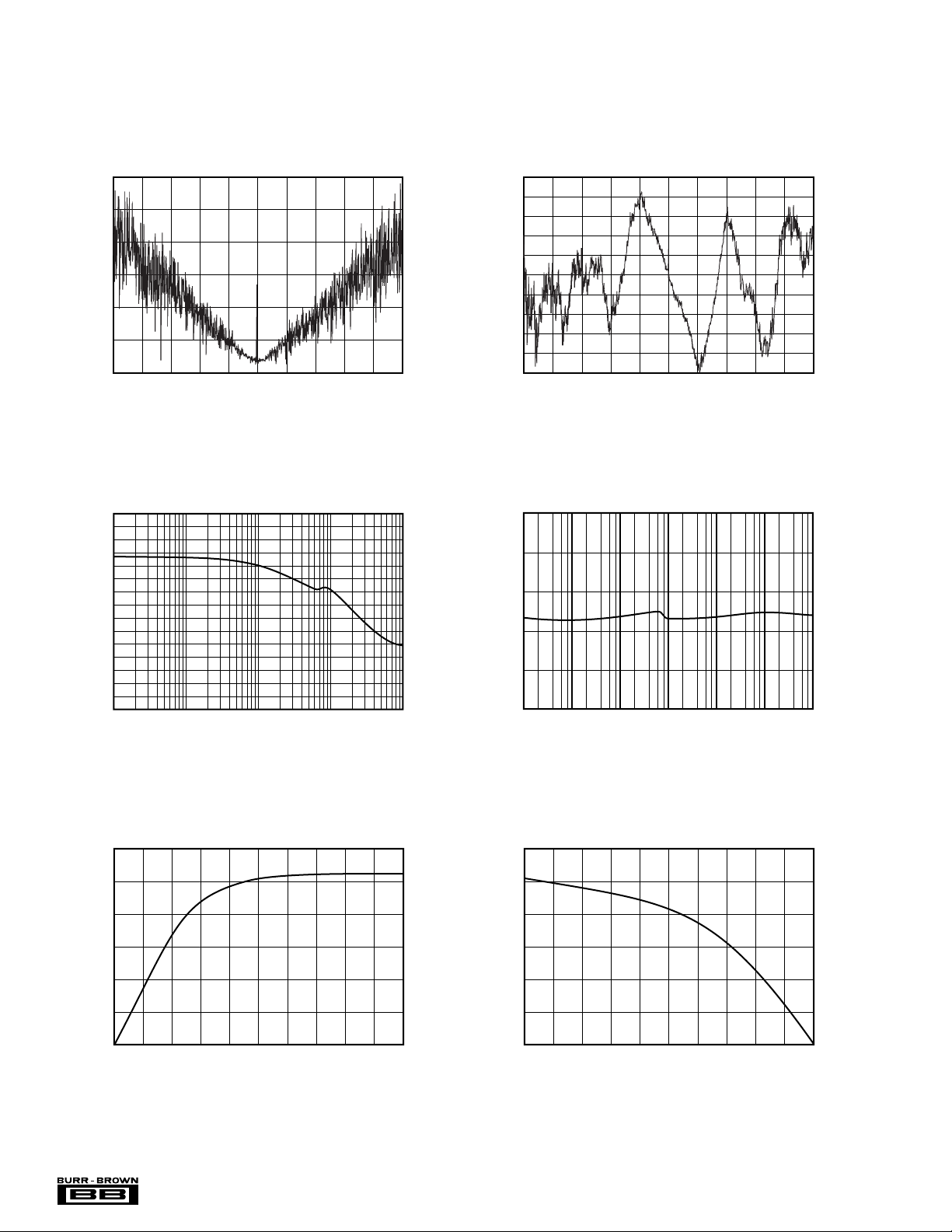
TYPICAL PERFORMANCE CURVES
At TA = +25°C, AVDD = DVDD = +5V, MCLK = 320kHz, REFEN LOW, BIASEN LOW, and external +2.5V reference, unless otherwise specified.
1.2
1
0.8
0.6
(ppm)
0.4
0.2
0
–5–4–3–2–1012345
110
105
rms NOISE
V
(V)
DIN
CMRR vs FREQUENCY
1.5
1.0
0.5
0
–0.5
–1.0
(ppm)
–1.5
–2.0
–2.5
–3.0
–3.5
–5–4–3–2–1012345
70
68
66
LINEARITY
(V)
V
DIN
PSRR vs FREQUENCY
CMRR (dB)
100
95
0.1 1 10 100 1000
Frequency (Hz)
30
25
20
(mA)
15
OUT
I
10
5
0
0 0.5 1.0 1.5 2.0 2.5 3.0 3.5 4.0 4.5 5.0
TYPICAL SINK CURRENT
(V)
V
OL
64
PSRR (dB)
62
60
0.1 1.0 10 100 1k 10k 100k
Frequency (Hz)
30
25
20
(mA)
15
OUT
I
10
5
0
0 0.5 1.0 1.5 2.0 2.5 3.0 3.5 4.0 4.5 5.0
TYPICAL SOURCE CURRENT
(V)
V
OL
®
ADS1201
4

TYPICAL PERFORMANCE CURVES (Cont.)
At TA = +25°C, AVDD = DVDD = +5V, MCLK = 320kHz, REFEN LOW, BIASEN LOW, and external +2.5V reference, unless otherwise specified.
110
105
100
95
CMRR (dB)
90
85
80
0 0.5 1.0 1.5 2.0 2.5 3.0 3.5 4.0 4.5
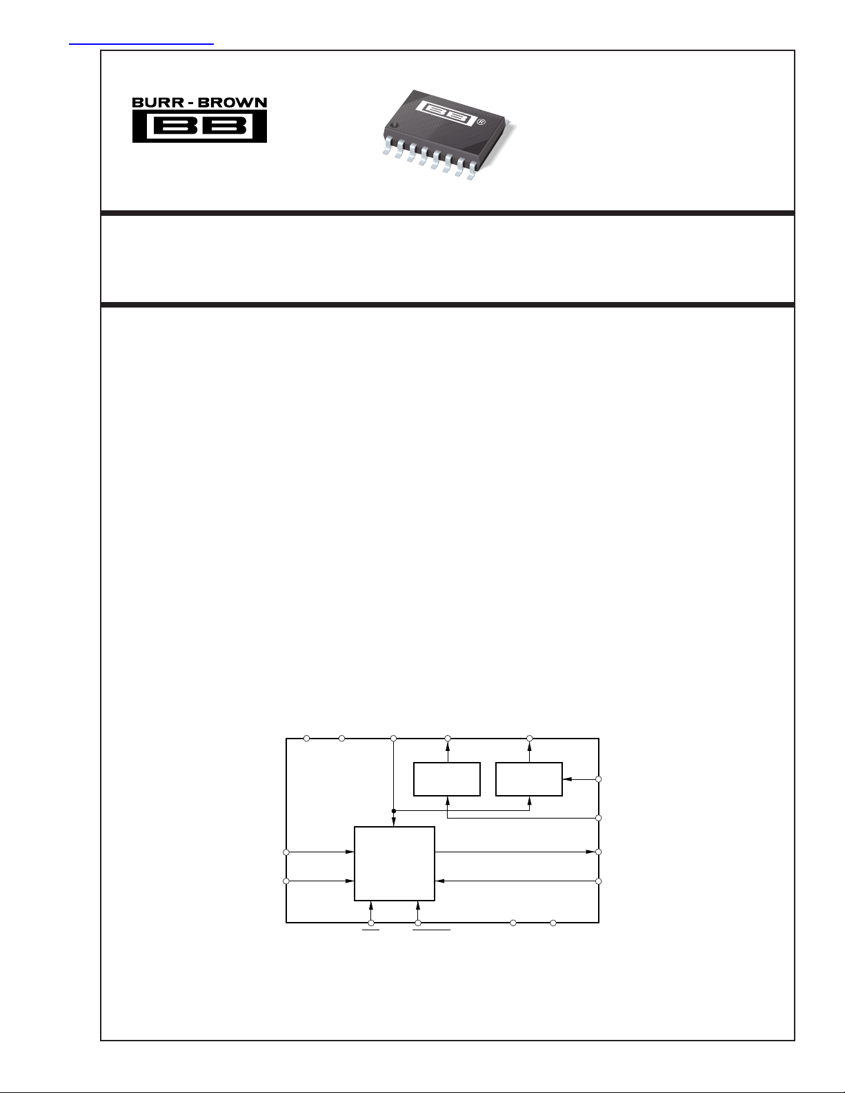
GENERAL DESCRIPTION
The ADS1201 is a single channel, second-order, CMOS
analog modulator designed for high resolution conversions
from dc to 1000Hz. The output of the converter (MOUT)
provides a stream of digital ones and zeros. The time
average of this serial output is proportional to the analog
input voltage. The combination of an ADS1201 and a
processor that is programmed to implement a digital filter
results in a high resolution A/D converter system. This
system allows flexibility with the digital filter design and is
capable of A/D conversion results that have a dynamic range
that exceeds 130dB (see Figure 1).
CMRR vs V
DIN
V
(V)
DIN
THEORY OF OPERATION
The differential analog input of the ADS1201 is implemented with a switched capacitor circuit. This switched
capacitor circuit implements a 2nd-order modulator stage
which digitizes the input signal into a binary output stream.
The input stage of the converter can be configured to sample
an analog signal or to perform a calibration which quantifies
offset and gain errors. The sample clock (MCLK) provides
the switched capacitor network and modulator clock signal
for the A/D conversion process, as well as the output data
framing clock. Different frequencies for this clock allows
for a variety of performance solutions in resolution and
signal bandwidth. The analog input signal is continuously
sampled by the A/D converter and compared to an internal
or external voltage reference. A digital stream appears at the
output of the converter. This digital stream accurately represents the analog input voltage over time.
Analog Supply
REF
MOUT
MCLK
DV
DGND
CAL
BIAS
16
EN
15
14
13
DD
12
11
10
9
EN
0.1µF
Digital
Supply
Processor
200Ω
200Ω
10µF
1
AV
DD
2
REF
OUT
3
REF
0.1µF
47pF47pF
IN
4
NIC
ADS1201
5
A
P
IN
6
A
N
IN
7
AGND
8
V
GAIN/OFFSET
BIAS
FIGURE 1. Connection Diagram for the ADS1201 Delta-Sigma Modulator Including External Processor.
5
ADS1201
®

Analog
Inputs
Switched
Capacitor
Analog
Input
1-Bit Data
2nd-Order
Charge-Balancing
A/D Converter
Stream
Processor
for
Filtering
Programmable Gain Amp
+
V
IN
V
REF
VIN–
FIGURE 2. Block Diagram of the ADS1201.
ANALOG INPUT STAGE
Analog Input
The input design topology of the ADS1201 is based on a
fully differential switched capacitor architecture. This input
stage provides the mechanism to achieve low system noise,
high common-mode rejection (100dB) and excellent power
supply rejection. The input impedance of the analog input is
dependent on the input capacitor and modulator clock frequency (MCLK), which is also the sampling frequency of
the converter. Figure 3 shows the basic input structure of the
ADS1201. The relationship between the input impedance of
the ADS1201 and the modulator clock frequency is:
E
A Input pedance
IN
Im ( )•Ω=
12
112
f
MCLK
The input impedance becomes a consideration in designs
where the source impedance of the input signal is significant. In this case, it is possible for a portion of the signal to
be lost across this external source impedance. The importance of this effect depends on the desired system performance.
There are two restrictions on the analog input signal to the
ADS1201. Under no conditions should the current into or
R
SW
AIN+
Switching Frequency
AIN–
= MCLK
8kΩ (typ)
R
SW
8kΩ (typ)
V
CM
C
12pF (typ)
C
12pF (typ)
High
Impedance
> 1GΩ
INT
INT
High
Impedance
> 1GΩ
FIGURE 3. Input Impedance of the ADS1201.
®
ADS1201
2nd-Order Modulator
1-Bit DAC
out of the analog inputs exceed 10mA. In addition, the
linearity of the device is guaranteed only when the analog
voltage applied to either input resides within the range
defined by AGND = > –30mV and < = AVDD + 30mV. If
either of the inputs exceed these limits, the input protection
diodes on the front end of the converter will begin to turn on.
This will induce leakage paths resulting in nonlinearities in
the conversion process.
For this reason, the 0V to 5V input range must be used with
caution. Should AVDD be 4.75V, the analog input signal
would swing outside the guaranteed specifications of the
device. Designs utilizing this mode of operation should
consider limiting the span to a slightly smaller range. Common-mode voltages are also a significant concern and must
be carefully analyzed.
Modulator
The modulator sampling frequency (MCLK) can be operated over a range of 20kHz to 1MHz. The frequency of
MCLK can be increased to improve the performance of the
converter or adjusted to comply with the clock requirements
of the application.
The modulator topology is fundamentally a 2nd-order, chargebalancing A/D converter, as the one conceptualized in Figure 4. The analog input voltage and the output of the 1-bit
DAC is differentiated, providing an analog voltage at X2 and
X3. The voltage at X2 and X3 are presented to their individual integrators. The output of these integrators progress
in a negative or positive direction. When the value of the
signal at X4 equals the comparator reference voltage, the
output of the comparator switches from negative to positive
or positive to negative, depending on its original state. When
the output value of the comparator switches from a HIGH to
LOW or vise versa, the 1-bit DAC responds on the next
clock pulse by changing its analog output voltage at X6,
causing the integrators to progress in the opposite direction.
The feedback of the modulator to the front end of the
integrators force the value of the integrator output to track
the average of the input.
6

REFERENCE CIRCUIT
There are two reference circuits included in the ADS1201
converter: V
for V
REF
(REFIN, REF
REF
OUT
) and V
. The circuitry
BIAS
is configured to allow the user to utilize the internal
reference on the chip or provide an external reference to the
converter (see Figure 5). The second reference, V
derived from V
, whether it is internal or external. V
REF
BIAS
, is
BIAS
is exclusively an output reference. This ratiometric relationship between V
REF
and V
reduces system errors when
BIAS
two separate bias voltages are required in the application.
REFERENCE INPUT (REFIN)
The reference input (REFIN) of the ADS1201 can be configured so that the 2.5V (nominal) internal or external reference
can be used in the conversion process. If the internal refer-
ence is used, the correct connection configuration is shown
in Figure 5a. The capacitor in this circuit is absolutely
required if low noise performance is desired.
An external reference can be used to reduce the noise in the
conversion process. If an external reference is used, care
should be taken to insure that the selected reference has low
noise performance. The appropriate connection circuit of an
external reference is shown in Figure 5b. The reference must
be configured with appropriate capacitors to reduce the high
frequency noise that may be contributed by the reference.
The input impedance of REFIN changes with the modulator
clock frequency. The relationship is:
E
TypicalREF Input pedance
IN
f
MCLK
Im
112
=
f
•
50
MCLK
X(t)
f
X
2
Integrator 1
S
X
FIGURE 4. Block Diagram of a Second-Order Modulator.
+5V
REF
MOUT
MCLK
DV
DGND
16
EN
15
14
13
DD
12
External
V
1µF
1
AV
DD
2
REF
OUT
3
REF
IN
4
NIC
ADS1201
5
P
A
IN
3
REF
Integrator 2
X
6
X
4
V
REF
D/A Converter
1
2
3
1µF
4
5
Comparator
AV
DD
REF
OUT
REF
IN
NIC
P
A
IN
ADS1201
MOUT
REF
MOUT
MCLK
DV
DGND
16
EN
15
14
13
DD
12
BIAS
CAL
11
10
9
EN
6
N
A
IN
7
AGND
8
V
GAIN/OFFSET
BIAS
(a) Internal Reference (b) External Reference
FIGURE 5. Two Voltage Reference Connection Alternatives for the ADS1201.
7
6
7
8
N
A
IN
AGND
V
BIAS
CAL
GAIN/OFFSET
BIAS
ADS1201
11
10
9
EN
®

The reference input voltage can vary between 2V and 3V.
Higher reference voltages will cause the full-scale range to
increase while the internal circuit noise of the converter
remains approximately the same. This will increase the LSB
weight but not the internal noise, resulting in increased
signal-to-noise ratio. Likewise, lower reference voltages
will decrease the signal-to-noise ratio.
The internal reference, which generates +2.5V, can be disabled when an external reference is used. This internal
reference is disabled with the REFEN pin. When the reference is disabled, the supply current (AVDD) of the converter
will reduce by approximately 1.6mA.
REFERENCE OUTPUT (VREF
OUT
)
The ADS1201 contains an internal +2.5V reference. When
using this feature, REFEN must be HIGH (see Figure 5).
Tolerances, drift, noise, and other specifications for this
reference are given in the Specifications table. Note that this
reference is not designed to sink or to source more than 1mA
of current. In addition, loading the reference with a dynamic
or variable load is not recommended. This can result in
small changes in reference voltage as the load changes.
VOLTAGE BIAS OUTPUT (V
The V
output voltage is dependent on the reference
BIAS
BIAS
)
input (REFIN) voltage and is approximately 1.33 times as
great. The output of V
is used to bias input signals of
BIAS
greater than 5V. If a resistor network is used in combination
with the V
output, the signal range can be scaled and
BIAS
level shifted to match the input range of the ADS1201.
Figure 6 shows a connection diagram which will allow the
ADS1201 to accept a ±10V input signal (20V full-scale
range). If BIASEN is HIGH, the voltage at V
3.3V (assumes a 2.5V nominal V
REF
).
BIAS
will be
REF
EN
LOW High Impedance
HIGH 2.5V (nominal)
TABLE I. Reference Enable.
R
1
V
IN
V
IN
3kΩ
+
R
2
3kΩ
–
R
1kΩ
REF
OUT
1
AV
0.1µF
1µF
3
R
1kΩ
4
DD
2
REF
OUT
3
REF
IN
4
NIC
ADS1201
5
A
P
IN
6
A
N
IN
7
AGND
8
V
GAIN/OFFSET
BIAS
REF
MOUT
MCLK
DV
DGND
CAL
BIAS
16
EN
15
14
13
DD
12
11
10
9
EN
0.1µF
Serial Data Out
Clock In
FIGURE 6. ±10V Bipolar Input Configuration Using V
t
1
t
t
2
3
t
MCLK
MOUT
4
t
6
t
5
Data Valid Data Valid Data Valid Data Valid
BIAS
.
SYMBOL
t
1
t
2
t
3
t
4
t
5
t
6
DOUT Valid after Clock Rising Edge
FIGURE 7. Timing Diagram for the Digital Interface of the ADS1201.
®
ADS1201
8
DESCRIPTION MIN TYP
Clock Period
Clock HIGH
Clock LOW
Clock Rise Time
Clock Fall Time
3125
1562.5
1562.5
6
6
MAX UNITS
ns
ns
ns
ns
ns
400
ns

BIAS
EN
LOW High Impedance
HIGH 1.33V • V
V
BIAS
REF
TABLE II. Bias Enable.
When enabled, the V
circuitry consumes approximately
BIAS
1mA with no external load. The maximum current into or
out of V
On power-up, external signals may be present before V
should not exceed 10mA.
BIAS
BIAS
is enabled. This can create a situation in which a negative
voltage is applied to the analog inputs, reverse biasing the
negative input protection diode of the ADS1201. This situation should not be a problem as long as the resistors R1 and
R2 limit the current being sourced by each analog input to be
under 10mA. A potential of 0V at the analog input pin (AINP
or AINN) should be used in the calculation.
DIGITAL OUTPUT
The timing diagram for the ADS1201 data retrieval is shown
in Figure 7. MCLK initiates the modulator process for the
ADS1201 and is used as a system clock by the ADS1201, as
well as a framing clock for data out. The modulator output
data, which is a serial stream, is available on the MOUT pin.
Typically, MOUT is read on the falling edge of MCLK.
Under any situation with MCLK, the duty cycle must be
kept constant for reliable, repeatable results.
An input differential signal of 0V will ideally produce a
stream of ones and zeros that are HIGH 50% of the time and
LOW 50% of the time. A differential input of 5V will
produce a stream of ones and zeros that are HIGH 90% of
the time. A differential input of –5V will produce a stream
of ones and zeros that are HIGH 10% of the time. The input
voltage versus the output modulator signal is shown in
Figure 8.
OFFSET and GAIN CALIBRATION
The ADS1201 offers a self-calibration function that is implemented with the GAIN/OFFSET and CALEN pins. Both
conditions provide an output stream of data, similar to
normal operation where the converter is configured to sample
an input signal at AIN.
The offset and gain errors of the ADS1201 are calibrated
independently. For best operation, the offset should be
calibrated first, followed by the gain. The calibration implementation timing diagram is shown in Figure 9. The calibration mode pins control the calibration functions of the
ADS1201.
Calibration should be performed once and then normal
operation can be resumed. Calibration of offset and gain is
recommended immediately after power-on and whenever
there is a “significant” change in the operating environment.
Significant changes in the operating environment include a
change of the MCLK frequency, MCLK duty cycle, power
Modulator Output
Analog Input
FIGURE 8. Analog Input versus Modulator Output of the ADS1201.
t
8
SYMBOL
t
9
t
11
t
t
NOTE: (1) T
CAL
GAIN/OFFSET
t
9
t
t
10
8
DESCRIPTION MIN
CAL and GAIN/OFFSET Rise Time
t
8
CAL and GAIN/OFFSET Fall Time
t
9
GAIN/OFFSET to CAL Setup Time
10
GAIN/OFFSET to CAL Hold Time
11
is the clock period of MCLK.
MCLK
+FS (Analog Input)
–FS (Analog Input)
TYP
10
10
0
(1)
2.5 T
MCLK
MAX UNITS
ns
ns
ns
ns
FIGURE 9. Timing Diagram for the Calibration Feature of the ADS1201.
9
®
ADS1201

GAIN/OFFSET CAL
0 1 Normal Mode
0 0 Offset Calibration, Analog inputs shorted
1 0 Full-Scale Calibration, Analog inputs are
EN
to ground internally.
referenced to V
internally.
REF
TABLE III. Calibration Enable.
supply, V
, or temperature. The amount of change which
REF
could cause a re-calibration is dependent on the application
and effective resolution of the system.
The results of the calibration calculations are stored in two
registers in the processor chip (see Figure 1). These two
calibration results can then be used to calibrate the input
signal results with one of the following formulas:
Equivalent Calibrated Output Code = FSC (FO1 – FO2)/(FO3 – FO2)
where FO
= Filter output code of an applied input voltage
1
FO
= Filter output code of the offset calibration
2
= Filter output code of the gain calibration
FO
3
FSC = Desired full-scale output
With a simple sinc filter, the calibrated A/D conversion
would equal:
Equivalent Calibrated Input Voltage = (N1 – N2) • V
where N
= number of ones counted (or digital equivalent
1
after filtering) over given time (t
N
= number of ones counted (or digital equivalent after filtering)
2
during offset calibration where t
N3 = number of ones counted (or digital equivalent after filtering)
during gain calibration where t13 = t
M
12
/(N3 – N2)
REF
) with an applied input voltage
= t
M
M
A system calibration can be performed by applying two
known voltage levels to the input of the converter. In this
situation, the GAIN/OFFSET and CALEN pins are not used.
Rather, the digital output of these two known voltages are
accumulated by the processor. With this data, the processor
can determine the calibration register values that are appropriate for the application.
LAYOUT CONSIDERATIONS
POWER SUPPLIES
The ADS1201 requires the digital supply (DVDD) to be no
greater than the analog supply (AVDD). Failure to observe
this condition could cause permanent damage to the
ADS1201. The best scheme is to power the analog section of
the design and AVDD from one +5V line and the digital
section and DVDD from a separate +5V line (from the same
supply). If there are separate analog and digital power
supplies for the ADS1201, a good design approach would be
to have the analog supply come up first, followed by the
digital supply. Another approach that can be used to control
the analog and digital power supply differences is shown in
Figure 10. In this circuit, a connection has been made
between the ADS1201 supply pins via a 10Ω resistor. The
combination of this resistor and the decoupling capacitors
provides some filtering between DVDD and AVDD.
The analog supply should be well regulated and low noise.
For designs requiring very high resolution from the ADS1201,
power supply rejection will be a concern. The requirements
for the digital supply are not strict. However, high frequency
noise on DVDD can capacitively couple into the analog
portion of the ADS1201. This noise can originate from
switching power supplies, microprocessors or digital signal
processors.
For either supply, high frequency noise will generally be
rejected by the external digital filter at integer multiples of
MCLK. Just below and above these frequencies, noise will
alias back into the pass-band of the digital filter, affecting
the conversion result.
Inputs to the ADS1201, such as AIN, REFIN, and MCLK,
should not be present before the analog and digital supplies
are on. Violating this condition could cause latch-up. If
these signals are present before the supplies are on, series
resistors should be used to limit the input current.
If one supply must be used to power the ADS1201, the
system’s analog supply should be used to power both AV
DD
and DVDD. Experimentation may be the best way to determine the appropriate connection between AVDD and DVDD.
GROUNDING
The analog and digital sections of the design should be
carefully and cleanly partitioned. Each section should have
its own ground plane with no overlap between them. AGND
should be connected to the analog ground plane as well as
all other analog grounds. DGND should be connected to the
digital ground plane and all digital signals referenced to this
plane.
The ADS1201 pinout is such that the converter is cleanly
separated into an analog and digital portion. This should
allow simple layout of the analog and digital sections of the
design.
For a signal converter system, AGND and DGND of the
ADS1201 can be connected together. Do not join the ground
planes, but connect the two with a moderate signal trace
underneath the converter. For multiple converters, connect
the two ground planes at one location as central to all of the
converters as possible. In some cases, experimentation may
be required to find the best point to connect the two planes
together. Experimentation may be the best way to determine
the appropriate connection between AGND and DGND.
DECOUPLING
Good decoupling practices should be used for the ADS1201
and for all components in the design. All decoupling capacitors, specifically the 0.1µF ceramic capacitors, should be
placed as close as possible to the pin being decoupled. A
1µF and 10µF capacitor, in parallel with the 0.1µF ceramic
capacitor, should be used to decouple AVDD to AGND. At
a minimum, a 0.1µF ceramic capacitor should be used to
decouple DVDD to DGND, as well as for the digital supply
on each digital component.
®
ADS1201
10

+5V
10Ω
1
AV
+
10µF
0.1µF
DD
2
REF
OUT
3
REF
IN
4
NIC
ADS1201
5
A
P
IN
6
A
N
IN
7
AGND
8
V
GAIN/OFFSET
BIAS
REF
MOUT
MCLK
DV
DGND
CAL
BIAS
16
EN
15
14
13
DD
0.1µF
12
11
10
9
EN
FIGURE 10. Power Supply Connection Using One Power Plane and One Digital Plane.
Isolated Power
+5V
87
100µA 100µA
12
REF200
5
3
10kΩ
4
6kΩ
1µF
0.1µF
DSP
1
AV
DD
2
REF
OUT
3
REF
IN
4
NIC
P
A
IN
N
A
IN
AGND
V
BIAS
ADS1201
GAIN/OFFSET
5
6
7
8
REF
MOUT
MCLK
DV
DGND
BIAS
CAL
16
EN
15
14
13
DD
EN
0.1µF
12
11
10
9
Opto
Coupler
Opto
Coupler
MDATA
+5V
SCLK
SDATA
+5V
MCLK
FIGURE 11. Bridge Transducer Interface with Current Excitation.
11
®
ADS1201

87
REF200
100µA 100µA
+5V
0.1µF
Isolated Power
+5V
12
1µF
1
AV
DD
2
REF
OUT
3
REF
IN
4
NIC
ADS1201
5
A
P
IN
PT100
6
A
N
IN
12.5kΩ
7
AGND
8
V
GAIN/OFFSET
BIAS
FIGURE 12. PT100 Interface with Current Excitation.
REF
MOUT
MCLK
DV
DGND
CAL
BIAS
DSP
16
EN
15
Opto
Coupler
MDATA
+5V
14
13
DD
SCLK
0.1µF
12
11
10
+5V
Opto
Coupler
9
EN
SDATA
MCLK
+5V
10kΩ
3
1/2
1
R
OPA2237
2
G
6
1/2
OPA2237
5
7
FIGURE 13. Geophone Interface.
0.1µF
0.1µF
1
2
3
4
5
6
7
8
AV
DD
REF
REF
NIC
A
P
IN
A
N
IN
AGND
V
BIAS
OUT
IN
ADS1201
GAIN/OFFSET
REF
MOUT
MCLK
DV
DGND
CAL
BIAS
DSP
16
EN
15
14
13
DD
MDATA
MCLK
SCLK
0.1µF
12
SDATA
11
10
9
EN
®
ADS1201
12

+5V
0.1µF
Isolated Power
+5V
10kΩ
1
R
G
3
OPA2237
2
6
OPA2237
5
1/2
10kΩ
10kΩ
1/2
AV
DD
1
0.1µF
2
REF
OUT
3
REF
IN
4
NIC
ADS1201
5
P
A
IN
6
N
A
IN
7
AGND
7
8
V
BIAS
REF
MOUT
MCLK
DV
DGND
CAL
GAIN/OFFSET
BIAS
EN
DD
EN
FIGURE 14. Single-Supply, High Accuracy Thermocouple Interface.
Floating Positive
HV+
Supply
DSP
16
15
Opto
Coupler
MDATA
+5V
14
13
SCLK
0.1µF
12
11
10
9
+5V
Opto
Coupler
SDATA
MCLK
Gate Drive
R
SENSE
R
Motor
SENSE
HV–
FIGURE 15. Motor Controller Sensing Circuit.
5.1V
0.1µF
0.1µF
DSP
1
AV
DD
2
REF
OUT
3
REF
IN
4
NIC
A
P
IN
A
N
IN
AGND
V
BIAS
ADS1201
GAIN/OFFSET
5
6
7
8
REF
MOUT
MCLK
DV
DGND
BIAS
CAL
16
EN
15
14
13
DD
EN
0.1µF
12
11
10
9
Opto
Coupler
Opto
Coupler
+5V
MDATA
MCLK
+5V
SCLK
SDATA
13
®
ADS1201
 Loading...