

Please be aware that an important notice concerning availability, standard warranty, and use in critical applications of Texas Instruments
查询ADS1112供应商查询ADS1112供应商
16-Bit Analog-to-Digital Converter with
Input Multiplexer and Onboard Reference
ADS1112
SBAS282D − JUNE 2003 − REVISED MARCH 2004
FEATURES
D COMPLETE DATA ACQUISITION SYSTEM IN
THE MSOP-10 AND LEADLESS QFN-STYLE
PACKAGES
D MEASUREMENTS FROM TWO DIFFERENTIAL
CHANNELS OR THREE SINGLE-ENDED
CHANNELS
2
D I
CINTERFACE—EIGHT ADDRESSES PIN-
SELECTABLE
D ONBOARD REFERENCE:
Accuracy: 2.048V ±0.05%
Drift: 5ppm/°C
D ONBOARD PGA
D ONBOARD OSCILLATOR
D 16 BITS, NO MISSING CODES
D INL: 0.01% of FSR max
D CONTINUOUS SELF-CALIBRATION
D SINGLE-CYCLE CONVERSION
D PROGRAMMABLE DATA RATE: 15SPS to
240SPS
D POWER SUPPLY: 2.7V to 5.5V
D LOW CURRENT CONSUMPTION: 240µA
DESCRIPTION
The ADS1112 is a precision, continuously self-calibrating
Analog-to-Digital (A/D) converter with two dif ferential or three
single-ended channels and up to 16 bits of resolution in the
small MSOP-10 and leadless QFN-style (small-outline,
no-lead) packages. The onboard 2.048V reference provides
an input range of ±2.048V differentially. The ADS1112 uses
2
an I
C-compatible serial interface and has two address pins
that allow a user to select one of the eight I
addresses. The ADS1112 operates from a single power
supply ranging from 2.7V to 5.5V.
The ADS1 112 can p erform c onversions at r ates o f 15, 30, 6 0,
or 240 samples per second (SPS). The onboard
programmable g ain a m plifier (PGA), which of fers gains of up
to eight, allow s smaller signals to be measured with high
resolution. In single-conversion mode, the ADS1112
automatically powers down after a conversion, greatly
reducing current cons umpti on during idle periods.
The ADS1112 is designed for applications requiring
high-resolution measurement, where space and power
consumption are maj or considerations . Typical applications
include portable instrumentation, industrial process control,
and smart transmitters.
2
C Slave
APPLICATIONS
D PORTABLE INSTRUMENTATION
D INDUSTRIAL PROCESS CONTROL
D SMART TRANSMITTERS
D CONSUMER GOODS
D FACTORY AUTOMATION
D TEMPERATURE MEASUREMENT
semiconductor products and disclaimers thereto appears at the end of this data sheet.
All trademarks are the property of their respective owners.
! !
www.ti.com
Copyright 2003−2004, Texas Instruments Incorporated
"###$
ADS1112
MSOP-10
DGS
−40°C to +85°C
BHU
ADS1112
SON-10
DRC
−40°C to +85°C
BHV
SBAS282D − JUNE 2003 − REVISED MARCH 2004
www.ti.com
ABSOLUTE MAXIMUM RATINGS
(1)
VDD to GND −0.3V to +6V
Input Current 100mA, Momentary
Input Current 10mA, Continuous
Analog Inputs, A0, A1, Voltage to GND −0.3V to VDD + 0.3V
SDA, SCL Voltage to GND −0.5V to 6V
Maximum Junction Temperature +150°C
Operating Temperature Range −40°C to +125°C
Storage Temperature Range −60°C to +150°C
precautions. Failure to observe proper handling and
installation procedures can cause damage.
ESD damage can range from subtle performance degradation
to complete device failure. Precision integrated circuits may
be more susceptible to damage because very small
parametric changes could cause the device not to meet its
published specifications.
Lead Tem perature (soldering, 10s) +300°C
(1)
Stresses above those listed under Absolute Maximum Ratings
may cause permanent damage to the device. Exposure to
absolute maximum conditions for extended periods may affect
device relia b i l i t y.
PACKAGE/ORDERING INFORMATION
PRODUCT PACKAGE-LEAD
(1)
For the most current specification and package information, refer to our web site at www.ti.com.
PACKAGE
DESIGNATOR
(1)
SPECIFIED
TEMPERATURE
RANGE
°
°
°
°
PACKAGE
MARKING
This integrated circuit can be damaged by ESD.
Texas Instruments recommends that all
integrated circuits be handled with appropriate
ORDERING NUMBER
ADS1112IDGST Tape and Reel, 250
ADS1112IDGSR Tape and Reel, 2500
ADS1112IDRCT Tape and Reel, 250
ADS1112IDRCR Tape and Reel, 3000
TRANSPORT MEDIA,
QUANTITY
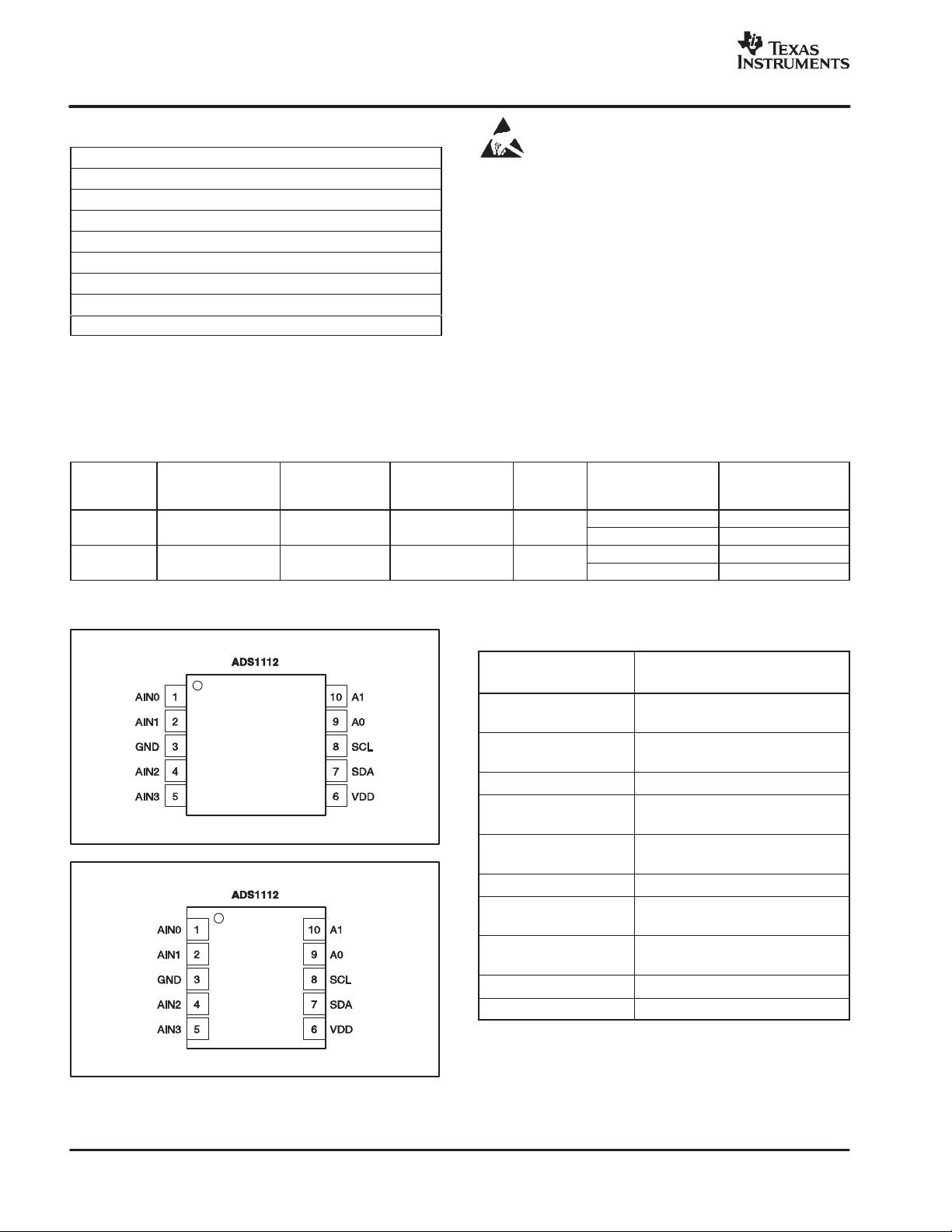
Top View
Top View
MSOP-10
SON-10
Terminal Functions
TERMINAL
NAME NO. DESCRIPTION
AIN0 1 Differential Channel 1; Positive Input
Single-ended Channel 1 Input
AIN1 2 Differential Channel 1; Negative Input
Single-ended Channel 2 Input
GND 3 Ground
AIN2 4 Differential Channel 2; Positive Input
Single-ended Channel 3 Input
AIN3 5 Differential Channel 2; Negative Input
Single-ended Common Input
VDD 6 Power Supply: 2.7V to 5.5V
SDA 7 Serial Data: Transmits and receives
data
SCL 8 Serial Clock Input: Clocks output
data on SDA
A0 9 I2C Slave Address Select
A1 10 I2C Slave Address Select
2

"###$
Resolution and No Missing Codes
Data Rate
Offset Error
Offset Drift
Offset vs VDD
Common-Mode Rejection
Supply Current
Power Dissipation
www.ti.com
SBAS282D − JUNE 2003 − REVISED MARCH 2004
ELECTRICAL CHARACTERISTICS
All specifications at −40°C to +85°C, VDD = 5V, and all PGAs, unless otherwise noted.
ADS1112
PARAMETER CONDITIONS
ANALOG INPUT
Full-Scale Input Voltage (V
Analog Input Voltage V
Differential Input Impedance 2.8/PGA MΩ
Common-Mode Input Impedance PGA = 1 3.5 MΩ
SYSTEM PERFORMANCE
Resolution and No Missing Codes DR = 00 12 12 Bits
Data Rate DR = 00 180 240 308 SPS
Output Noise See Typical Characteristic Curves
Integral Nonlinearity DR = 11, PGA = 1, End Point Fit
Offset Error PGA = 1 1.2 8 mV
Offset Drift PGA = 1 1.2 µV/°C
Offset vs VDD PGA = 1 800 µV/V
Channel Offset Match Match between any two channels 30 µV
Gain Error
PGA Gain Error Match
Gain Error Drift
Gain vs VDD 80 ppm/V
Channel Gain Match Match between any two channels 0.01 %
Common-Mode Rejection At DC and PGA = 8 95 105 dB
DIGITAL INPUT/OUTPUT
Logic Level
V
V
V
Input Leakage
I
H
I
L
POWER-SUPPLY REQUIREMENTS
Power-Supply Voltage VDD 2.7 5.5 V
Supply Current Power-Down 0.05 2 µA
Power Dissipation VDD = 5.0V 1.2 1.75 mW
(1)
(2)
(3)
(3)
(3)
(3)
IH
IL
OL
99% of full-scale.
FSR = full-scale range = 2 × 2.048V/PGA = 4.096V/PGA.
Includes all errors from onboard PGA and reference.
) − (V
IN+
to GND or V
IN+
PGA = 2 3.5 MΩ
PGA = 4 1.8 MΩ
PGA = 8 0.9 MΩ
DR = 01 14 14 Bits
DR = 10 15 15 Bits
DR = 11 16 16 Bits
DR = 01 45 60 77 SPS
DR = 10 22 30 39 SPS
DR = 11 11 15 20 SPS
PGA = 2 0.7 4 mV
PGA = 4 0.5 2.5 mV
PGA = 8 0.4 1.5 mV
PGA = 2 0.6 µV/°C
PGA = 4 0.3 µV/°C
PGA = 8 0.3 µV/°C
PGA = 2 400 µV/V
PGA = 4 200 µV/V
PGA = 8 150 µV/V
Match between any two PGA gains 0.02 0.10 %
At DC and PGA = 1 100 dB
IOL = 3mA GND 0.4 V
VIH = 5.5V 10 µA
VIL = GND −10 µA
Active Mode 240 350 µA
VDD = 3.0V 0.675 mW
) ±2.048/PGA V
IN−
to GND GND − 0.2 VDD + 0.2 V
IN−
(1)
MIN TYP MAX
±0.004 ±0.010 % of FSR
0.05 0.40 %
5 40 ppm/°C
0.7 • VDD 6 V
GND − 0.5 0.3 • VDD V
UNIT
(2)
3
"###$
SBAS282D − JUNE 2003 − REVISED MARCH 2004
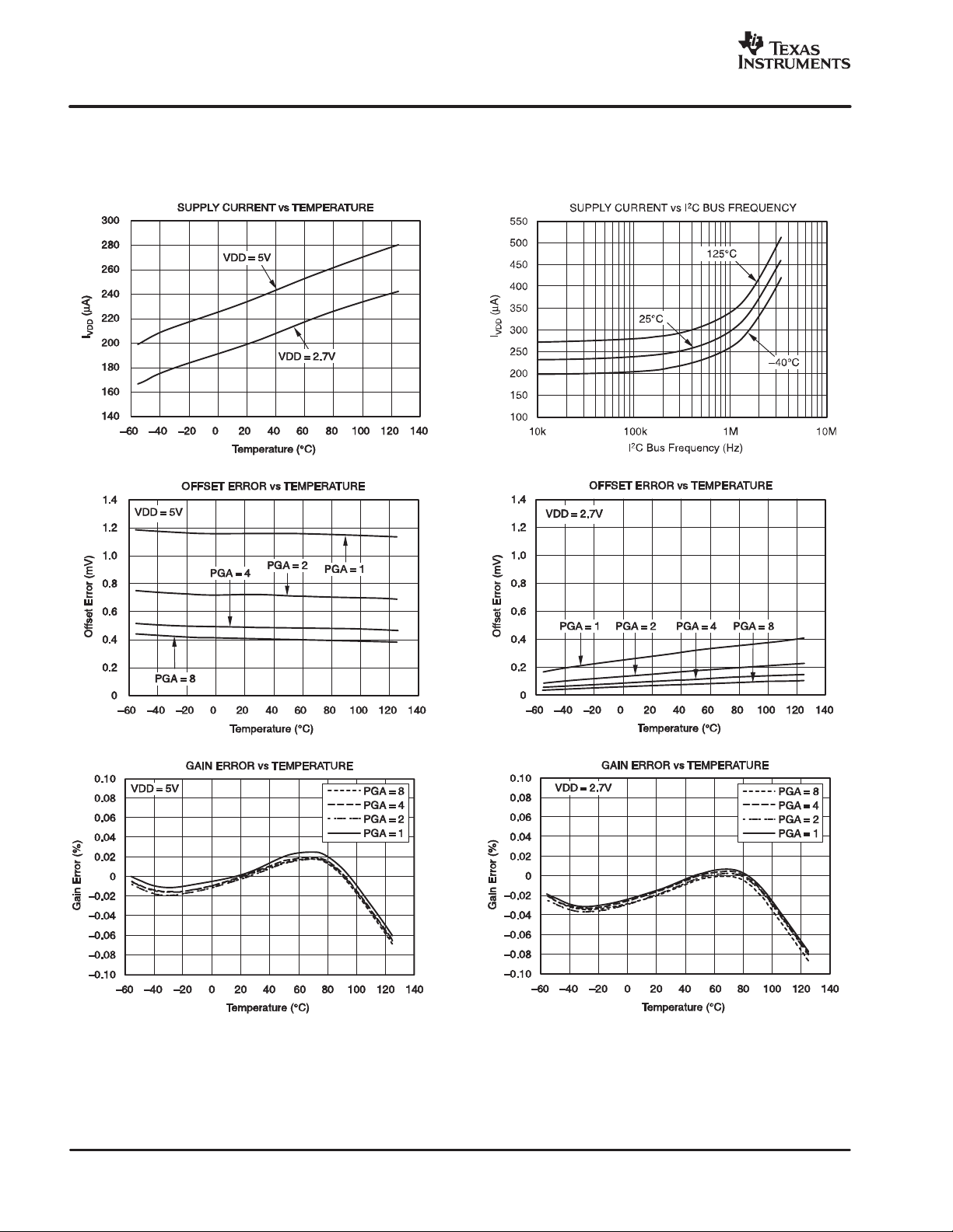
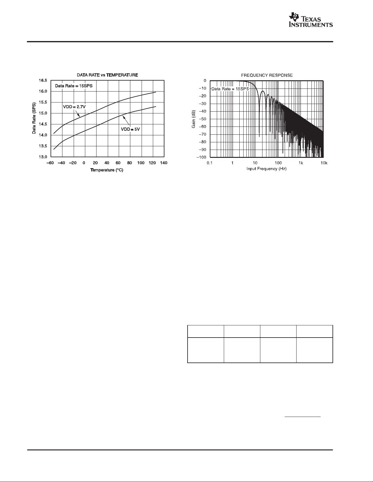
TYPICAL CHARACTERISTICS
At TA = 25°C and VDD = 5V, unless otherwise noted.
www.ti.com
4
www.ti.com
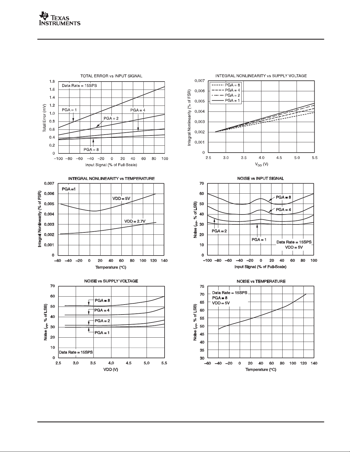
TYPICAL CHARACTERISTICS (continued)
At TA = 25°C and VDD = 5V, unless otherwise noted.
"###$
SBAS282D − JUNE 2003 − REVISED MARCH 2004
5
"###$
SBAS282D − JUNE 2003 − REVISED MARCH 2004
TYPICAL CHARACTERISTICS (continued)
At TA = 25°C and VDD = 5V, unless otherwise noted.
www.ti.com
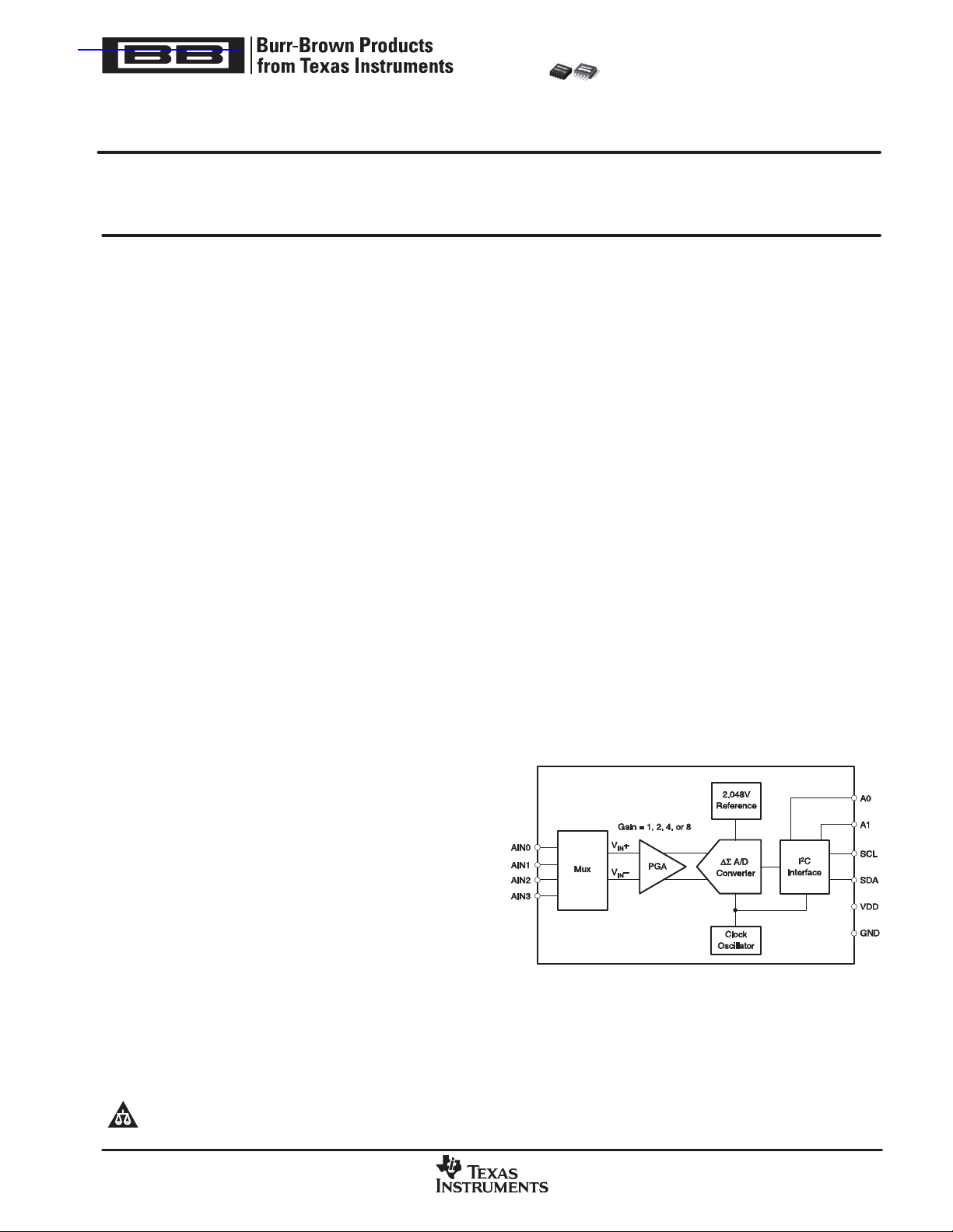
THEORY OF OPERATION
The ADS1112 is a 16-bit, self-calibrating, delta-sigma A/D
converter with an input multiplexer. Extremely easy to design with and configure, the ADS1 112 allows precise measurements to be obtained with a minimum of effort.
The ADS1112 consists of a delta-sigma A/D converter
core with adjustable gain, a 2.048V reference, a clock oscillator, and an I
scribed in detail in the sections that follow.
ANALOG-TO-DIGITAL CONVERTER
The ADS1112 A/D converter core consists of a differential
switched-capacitor delta-sigma modulator followed by a
digital filter. The modulator measures the voltage difference between the positive and negative analog inputs selected by the input multiplexer and compares it to a reference voltage, which, in the ADS1112, is 2.048V. The digital
filter receives a high-speed bitstream from the modulator
and outputs a code, which is a number proportional to the
input voltage.
MULTIPLEXER
The ADS1112 has an input multiplexer that provides for
two differential or three single-ended input channels. Two
bits in the configuration register control the multiplexer
setting.
VOLTAGE REFERENCE
The ADS1112 contains an onboard 2.048V voltage reference. This reference is always used as the ADC voltage
reference; an external reference cannot be connected.
The ADS1112 voltage reference is internal only, and cannot be measured directly or used by external circuitry.
2
C interface. Each of these blocks are de-
The onboard reference specifications are part of the overall gain and drift specifications of the ADS1112. The converter drift and gain error specifications reflect the performance of the onboard reference as well as the
performance of the A/D converter core. There are no separate specifications for the onboard reference itself.
OUTPUT CODE CALCULATION
The output code is a scaled value that is proportional, except for clipping, to the voltage difference between the t wo
analog inputs. The output code is confined to a finite range
of numbers; this range depends on the number of bits
needed to represent the code. The number of bits needed
to represent the output code for the ADS1 112 depends on
the data rate, as shown in Table 1.
NUMBER OF
DATA RATE
15SPS 16 −32,768 32,767
30SPS 15 −16,384 16,383
60SPS 14 −8192 8191
240SPS 12 −2048 2047
BITS
Table 1. Minimum and Maximum Codes
For a minimum output code of Min Code, gain setting of the
PGA, and positive and negative input voltages of V
, the output code is given by the expression:
V
IN−
Output Code + −1 Min Code PGA
In the previous expression, it is important to note that the
negated minimum output code is used. The ADS1112
outputs codes in binary two’s complement format, so the
MINIMUM
CODE
(V
IN)
2.048V
MAXIMUM
) * (V
CODE
IN+
IN*
and
)
6

www.ti.com
DATA RATE
"###$
SBAS282D − JUNE 2003 − REVISED MARCH 2004
absolute values of the minima and maxima are not the
n−1
same; the maximum n-bit code is 2
minimum n-bit code is −1 × 2
n−1
.
− 1, while the
For example, the ideal expression for output codes with a
data rate of 16SPS and PGA = 2 is:
Output Code + 16384 2
) * (V
IN)
2.048V
IN*
)
(V
The ADS1112 outputs all codes right-justified and
sign-extended. This feature makes it possible to perform
averaging on the higher data rate codes using only a 16-bit
accumulator.
Table 2 shows the output codes for various input levels.
SELF-CALIBRATION
The previous expressions for the ADS1112 output code do
not account for the gain and offset errors in the modulator.
To compensate for these, the ADS1112 incorporates
self-calibration circuitry.
The self-calibration system operates continuously and
requires no user intervention. No adjustments can be
made to the self-calibration system, and none need to be
made. The self-calibration system cannot be deactivated.
values depend on the PGA setting. The switching clock is
generated by the onboard clock oscillator, so its frequency
(nominally 275kHz) is dependent on supply voltage and
temperature.
The common-mode and differential input impedances are
different. For a gain setting of the PGA, the differential
input impedance is typically:
2.8MΩ/PGA
The common-mode impedance also depends on the PGA
setting. See the Electrical Characteristics for details.
The typical value of the input impedance often cannot be
neglected. Unless the input source has a low impedance,
the ADS1112 input impedance may affect the
measurement accuracy. For sources with high output
impedance, buffering may be necessary. Bear in mind,
however, that active buffers introduce noise, and also
introduce of fset and gain errors. All of these factors should
be considered in high-accuracy applications.
Because the clock oscillator frequency drifts slightly with
temperature, the input impedances will also drift. For many
applications, this input impedance drift can be neglected,
and the expression given above for typical input
impedance can be used.
The offset and gain error figures shown in the Electrical
Characteristics include the effects of calibration.
CLOCK OSCILLATOR
The ADS1112 features an onboard clock oscillator, which
drives the operation of the modulator and digital filter. The
Typical Characteristics show variations in data rate over
supply voltage and temperature.
It is not possible to operate the ADS1112 with an external
system clock.
INPUT IMPEDANCE
The ADS1112 uses a switched-capacitor input stage. To
external circuitry, it looks roughly like a resistance. The
resistance value depends on the capacitor values and the
rate at which they are switched. The switching frequency
is the same as the modulator frequency; the capacitor
(1)
−2.048V
15SPS 8000
30SPS C000
60SPS E000
240SPS F800
(1)
Differential input only; do not drive the ADS1112 inputs below −200mV.
H
H
H
H
−1LSB ZERO +1LSB +2.048V
FFFF
H
FFFF
H
FFFF
H
FFFF
H
ALIASING
If frequencies are input to the ADS1112 that exceed half
the data rate, aliasing will occur. To prevent aliasing, the
input signal must be bandlimited. Some signals are
inherently bandlimited. For example, the output of a
thermocouple, which has a limited rate of change, may
nevertheless contain noise and interference components.
These nuisance factors can fold back into the sampling
band just as with any other signal.
The ADS1112 digital filter provides some attenuation of
high-frequency noise, but the digital filter Sinc
response cannot completely replace an anti-aliasing filter.
For a few applications, some external filtering may be
needed; in such instances, a simple RC filter will suffice.
When designing an input filter circuit, remember to take
into account the interaction between the filter network and
the input impedance of the ADS1112.
DIFFERENTIAL INPUT SIGNAL
0000
0000
0000
0000
H
H
H
H
0001
0001
0001
0001
H
H
H
H
7FFF
3FFF
1FFF
07FF
1
frequency
H
H
H
H
Table 2. Output Codes for Different Input Signals
7

"###$
SBAS282D − JUNE 2003 − REVISED MARCH 2004
USING THE ADS1112
OPERATING MODES
The ADS1112 operates in one of two modes: continuousconversion or single-conversion.
In continuous-conversion mode, the ADS1112 continuously performs conversions. Once a conversion has been
completed, the ADS1112 places the result in the output
register and immediately begins another conversion.
In single-conversion mode, the ADS1112 waits until the
ST/DRDY
this happens, the ADS1112 powers up and performs a
single conversion. After the conversion completes, the
ADS1112 places the result in the output register, resets t h e
ST/DRDY
ST/DRDY
When switched from continuous-conversion mode to
single conversion mode, the ADS1112 completes the
current conversion, resets the ST/DRDY
powers down.
RESET AND POWER-UP
When the ADS1112 powers up, it automatically performs
a reset. As part of the reset process, the ADS1112 sets all
of the bits in the configuration register to their default
settings.
The ADS1112 responds to the I
command. When the ADS1112 receives a General Call
Reset, it performs an internal reset, exactly as though it
had just been powered on.
I2C INTERFACE
The ADS1112 communicates through an I2C
(inter-integrated circuit) interface. I
open-drain interface supporting multiple devices and
masters on a single bus. Devices on the I
the bus lines LOW by connecting them to ground; they
never drive the bus lines HIGH. Instead, the bus wires are
pulled HIGH by pull-up resistors, so the bus wires are
HIGH when no device is driving them LOW. This way, two
devices cannot conflict; if two devices drive the bus
simultaneously, there is no driver contention.
Communication on the I
between two devices, one acting as the master and the
other as the slave. Both masters and slaves can read and
write, but slaves can only do so under the direction of the
master. Some I
but the ADS1112 can only act as a slave device.
bit in the conversion register is set to 1. When
bit to 0, and powers down. Writing a 1 to
while a conversion is in progress has no effect.
bit to 0, and
2
C General Call Reset
2
C is a two-wire
2
C bus only drive
2
C bus always takes place
2
C devices can act as masters or slaves,
www.ti.com
2
An I
C bus consists of two lines, SDA and SCL. SDA
carries data; SCL provides the clock. All data is
transmitted across the I2C bus in groups of eight bits. To
send a bit on the I
2
C bus, the SDA line is driven to the
appropriate level while SCL is LOW (a LOW on SDA
indicates the bit is zero; a HIGH indicates the bit is one).
Once the SDA line has settled, the SCL line is brought
HIGH, then LOW. This pulse on SCL clocks the SDA bit
into the receiver’s shift register.
2
The I
C bus is bidirectional: the SDA line is used both for
transmitting and receiving data. When a master reads from
a slave, the slave drives the data line; when a master
sends to a slave, the master drives the data line. The
master always drives the clock line. The ADS1112 never
drives SCL, because it cannot act as a master. On the
ADS1112, SCL is an input only.
Most of the time the bus is idle; no communication occurs
place, and both lines are HIGH. When communication is
taking place, the bus is active. Only master devices can
start a communication and initiate a START condition on
the bus. Normally, the data line is only allowed to change
state while the clock line is LOW. If the data line changes
state while the clock line is HIGH, it is either a START
condition or its counterpart, a STOP condition. A START
condition occurs when the clock line is HIGH and the data
line goes from HIGH to LOW. A STOP condition occurs
when the clock line is HIGH and the data line goes from
LOW to HIGH.
After the master issues a ST ART condition, it sends a byte
that indicates which slave device it wants to communicate
with. This byte is called the address byte. Each device on
2
an I
C bus has a unique 7-bit address to which it responds.
(Slaves can also have 10-bit addresses; see the I
2
specification for details.) The master sends an address in
the address byte, together with a bit that indicates whether
it wishes to read from or write to the slave device.
Every byte transmitted on the I
2
C bus, whether it is
address or data, is acknowledged with an acknowledge
bit. When a master has finished sending a byte (eight data
bits) to a slave, it stops driving SDA and waits for the s la ve
to acknowledge the byte. The slave acknowledges the
byte by pulling SDA LOW. The master then sends a clock
pulse to clock the acknowledge bit. Similarly, when a
master has finished reading a byte, it pulls SDA LOW to
acknowledge this to the slave. It then sends a clock pulse
to clock the bit. (The master always drives the clock line.)
A not-acknowledge is performed by simply leaving SDA
HIGH during an acknowledge cycle. If a device is not
present on the bus, and the master attempts to address it,
it will receive a not-acknowledge because no device is
present at that address to pull the line LOW.
C
8

www.ti.com
"###$
SBAS282D − JUNE 2003 − REVISED MARCH 2004
When a master has finished communicating with a slave,
it may issue a STOP condition. When a STOP condition is
issued, the bus becomes idle again. A master may also
issue another ST ART condition. When a START condition
is issued while the bus is active, it is called a repeated
START condition.
A timing diagram for an ADS1112 I
2
C transaction is shown
in Figure 1. The parameters for this diagram are given in
Table 3.
SERIAL BUS ADDRESS
To program the ADS1112, the master must first address
slave devices via a slave address byte. The slave address
byte consists of seven address bits, and a direction bit
indicating the intent of executing a read or write operation.
The ADS1112 features two address pins, A0 and A1, that
set the I
logic high, or left unconnected (floating), allowing eight
2
C address. These pins can be set to a logic low,
addresses to be selected with only two pins as shown in
Table 4. The state of pins A0 and A1 is sampled on
2
power-up or after an I
C general call, and should be set
prior to any activity on the interface.
I2C GENERAL CALL
The ADS1112 responds to the I2C General Call address
(0000000) if the eighth bit is 0. The device will
acknowledge the General Call address and respond to
commands in the second byte. If the second byte is
00000100 (04h), the ADS1112 will latch the status of the
address pins, A0 and A1, but not perform a reset. If the
second byte is 00000110 (06h), the ADS1112 will latch the
status of the address pins and reset the internal registers.
PARAMETER
SCLK operating frequency
Bus free time between START and STOP condition
Hold time after repeated START condition.
After this period, the first clock is generated.
Repeated START condition setup time
Stop condition setup time
Data hold time
Data setup time
SCLK clock LOW period
SCLK clock HIGH period
Clock/data fall time
Clock/data rise time
Figure 1. I2C Timing Diagram
FAST MODE HIGH-SPEED MODE
MIN MAX MIN MAX
t
(SCLK)
t
(BUF)
t
(HDSTA)
t
(SUSTA)
t
(SUSTO)
t
(HDDAT)
t
(SUDAT)
t
(LOW)
t
(HIGH)
600 160 ns
600 160 ns
600 160 ns
600 160 ns
0 0 ns
100 10 ns
1300 160 ns
600 60 ns
t
F
t
R
0.4 3.4 MHz
300 160 ns
300 160 ns
Table 3. Timing Diagram Definitions
UNITS
9

"###$
SBAS282D − JUNE 2003 − REVISED MARCH 2004
www.ti.com
A0 A1 SLAVE ADDRESS
0 0 1001000
0 Float 1001001
0 1 1001010
1 0 1001100
1 Float 1001101
1 1 1001110
Float 0 1001011
Float 1 1001111
Float Float Invalid
Table 4. Address Pins and Slave Address for the
ADS1112.
I2C DATA RATES
The I2C bus operates in one of three speed modes.
Standard mode allows a clock frequency of up to 100kHz;
fast mode permits a clock frequency of up to 400kHz; and
high-speed mode (also called Hs mode), which allows a
clock frequency of up to 3.4MHz. The ADS1112 is fully
compatible with all three modes.
No special action needs to be taken to use the ADS1112
in standard or fast modes, but high-speed mode must be
activated. To activate high-speed mode, send a special
address byte of 00001xxx following the START condition,
where xxx are bits unique to the Hs-capable master. This
byte is called the Hs master code. (Note that this is dif ferent
from normal address bytes; the low bit does not indicate
read/write status.) The ADS1112 will not acknowledge this
byte; the I
2
C specification prohibits acknowledgment of
the Hs master code. On receiving a master code, the
ADS1112 will switch on its Hs mode filters, and
communicate at up to 3.4MHz. The ADS1112 will switch
out of Hs mode with the next STOP condition.
For more information on high-speed mode, consult the I
2
specification.
REGISTERS
The ADS1 112 has two registers that are accessible via its
2
C port. The output register contains the result of the last
I
conversion; the configuration register allows the user to
change the ADS1112 operating mode and query the status
of the device.
OUTPUT REGISTER
The 16-bit output register contains the result of the last
conversion in binary two’s complement format. Following
reset or power-up, the output register is cleared to zero,
and remains zero until the first conversion is completed.
The output register format is shown in Table 5.
C
BIT 15 14 13 12 11 10 9 8 7 6 5 4 3 2 1 0
NAME D15 D14 D13 D12 D11 D10 D9 D8 D7 D6 D5 D4 D3 D2 D1 D0
Table 5. Output Register
10

www.ti.com
"###$
SBAS282D − JUNE 2003 − REVISED MARCH 2004
CONFIGURATION REGISTER
The 8-bit configuration register can be used to control the
ADS1112 operating mode, input selection, data rate, and
PGA settings. The configuration register format is shown
in Table 6. The default setting is 8C
BIT 7 6 5 4 3 2 1 0
NAME ST/DRDY INP1 INP0 SC DR1 DR0 PGA1 PGA0
DEFAULT 1 0 0 0 1 1 0 0
Table 6. Configuration Register
Bit 7: ST/DRDY
The meaning of the ST/DRDY bit depends on whether it is
being written to or read from.
In single conversion mode, writing a 1 to the ST/DRDY
causes a conversion to start, and writing a 0 has no effect.
In continuous conversion mode, the ADS1 112 ignores the
value written to ST/DRDY
When read, ST/DRDY
.
indicates whether the data in the
output register is new data. If ST/DRDY
read from the output register is new , and has not been read
before. If ST/DRDY
is 1, the data just read from the output
register has been read before.
The ADS1112 sets ST/DRDY
to 0 when it writes data into
the output register. It sets ST/DRDY
bits in the configuration register have been read. (Note that
the read value of the bit is independent of the value written
to this bit.)
In continuous-conversion mode, use ST/DRDY
determine when new conversion data is ready. If
ST/DRDY
is 1, the data in the output register has already
been read, and is not new. If it is 0, the data in the output
register is new, and has not yet been read.
In single-conversion mode, use ST/DRDY to determine
when a conversion has completed. If ST/DRDY
output register data is old, and the conversion is still in
process; if it i s 0 , the output register data is the result of the
new conversion.
Note that the output register is returned from the ADS1 112
before the configuration register. The state of the
ST/DRDY
bit applies to the data just read from the output
register, and not to the data from the next read operation.
.
H
is 0, the data just
to 1 after any of the
to
is 1, the
bit
Bits 6-5: INP
INP controls which two of the four analog inputs are used
to measure data in the ADC. This is shown in Table 7. By
selecting these b i t s , the ADS1112 can be used to measure
two differential channels or three single ended channels
referenced to AIN3.
INP1 INP0 V
(1)
0
0 1 AIN2 AIN3
1 0 AIN0 AIN3
1 1 AIN1 AIN3
(1)
Default setting.
(1)
0
IN+
AIN0 AIN1
V
IN−
Table 7. INP Bits.
Bit 4: SC
SC controls whether the ADS1112 is in continuous
conversion or single conversion mode. When SC is 1, the
ADS1112 is in single conversion mode; when SC is 0, it is
in continuous conversion mode. The default setting is 0.
Bits 3-2: DR
Bits 3 and 2 control the ADS1112 data rate, as shown in
Table 8.
DR1 DR0 DATA RATE RESOLUTION
0 0 240SPS 12 Bits
0 1 60SPS 14 Bits
1 0 30SPS 15 Bits
(1)
1
(1)
Default setting.
(1)
1
15SPS
(1)
16 Bits
(1)
Table 8. INP Bits.
Bits 1-0: PGA
Bits 1 and 0 control the ADS1112 gain setting, as shown
in Table 9.
PGA1 PGA0 GAIN
0
(1)
Default setting.
(1)
0 1 2
1 0 4
1 1 8
(1)
0
(1)
1
Table 9. PGA Bits
11

"###$
SBAS282D − JUNE 2003 − REVISED MARCH 2004
www.ti.com
READING FROM THE ADS1112
To read the output register and the configuration register
from the ADS1112, first address the ADS1112 for reading,
then read three bytes. The first two bytes will be the output
register’s contents, and the third will be the configuration
register’s contents.
It is not required to read the configuration register byte. It
is permissible to read fewer than three bytes during a read
operation.
Reading more than three bytes from the ADS1112 has no
effect. All bytes following the third will be FF
It is possible to ignore the ST/DRDY
the ADS1112 output register at any time, without regard to
whether a new conversion is complete. If the output
bit and read data from
.
H
register is read more than once during a conversion cycle,
it will return the same data each time. New data will be
returned only when the output register has been updated.
A timing diagram of a typical ADS1112 read operation is
shown in Figure 2.
WRITING TO THE ADS1112
To write to the configuration register, first address the
ADS1112 for writing, and send one byte. The byte will be
written to the configuration register. Note that data cannot
be written to the output register.
Writing more than one byte to the ADS1 112 has no effect.
The ADS1112 will ignore any bytes sent to it after the first
one, and it will only acknowledge the first byte.
A timing diagram of a typical ADS1112 write operation is
shown in Figure 3.
12
Figure 2. Timing Diagram for Reading From the ADS1112
Figure 3. Timing Diagram for Writing To the ADS1112

www.ti.com
"###$
SBAS282D − JUNE 2003 − REVISED MARCH 2004
APPLICATIONS INFORMATION
The sections that follow give example circuits and tips for
using the ADS1112 in various situations.
BASIC CONNECTIONS
For many applications, connecting the ADS1112 is
extremely simple. A basic connection diagram for the
ADS1112 is shown in Figure 4.
Pull-up resistors are required on both the SDA and SCL
2
lines because I
C bus drivers are open-drain. The size of
these resistors depends on the bus operating speed and
capacitance of the bus lines. Higher-value resistors
consume less power, but increase the transition times on
the bus, limiting the bus speed. Lower-value resistors
allow higher speed at the expense of higher power
consumption. Long bus lines have higher capacitance and
require smaller pull-up resistors to compensate. The
resistors should not be too small; if they are, the bus drivers
may not be able to pull the bus lines low.
CONNECTING MULTIPLE DEVICES
Connecting multiple ADS1112s to a single bus is trivial.
Using pins A1 and A0, the ADS1112 can be set to one of
eight different I
ADS1112s is given in Figure 5. Up to eight ADS1112s
(using different states of pins A1 and A0) can be connected
to a single bus.
2
C addresses. An example showing three
Figure 4. Typical Connections of the ADS1112
The fully differential voltage input of the ADS1112 is ideal
for connection to differential sources with moderately low
source impedance, such as bridge sensors and
thermistors. Although the ADS1112 can read bipolar
differential signals, it cannot accept negative voltages on
either input. It may be helpful to think of the ADS1112
positive voltage input as non−inverting, and of the negative
input as inverting.
When the ADS1112 is converting, it draws current in short
spikes. The 0.1µF bypass capacitor supplies the
momentary bursts of extra current needed from the supply.
The ADS1112 interfaces directly to standard mode, fast
mode, and high-speed mode I
microcontroller’s I
and non-multiple-master I
2
C peripheral, including master-only
2
C peripherals, will work with the
2
C controllers. Any
ADS1112. The ADS1112 does not perform
clock-stretching (that is, it never pulls the clock line low),
so it is not necessary to provide for this unless
clock-stretching devices are on the same I2C bus.
Figure 5. Connecting Multiple ADS1112s
13

"###$
SBAS282D − JUNE 2003 − REVISED MARCH 2004
Note that only one set of pull-up resistors is needed per
bus. The pull-up resistor values may need to be lowered
slightly to compensate for the additional bus capacitance
presented by multiple devices and increased line length.
www.ti.com
Figure 7. Using GPIO with a Single ADS1112
Figure 6. Connecting Multiple Device Types
The TMP100 and DAC8574 devices detect their I2C bus
addresses based on the states of pins. In the example, the
TMP100 has the address 1001111, and the DAC8574 has
the address 1001 100. Consult the DAC8574 and TMP100
data sheets, located at www.ti.com, for further details.
USING GPIO PORTS FOR I2C
Most microcontrollers have programmable input/output
pins that can be set in software to act as inputs or outputs.
2
If an I
C controller is not available, the ADS1112 can be
connected to GPIO pins and the I
simulated, or “bit-banged,” in software. An example of this
for a single ADS1112 is shown in Figure 7.
2
C bus protocol
Bit-banging I2C with GPIO pins can be done by setting the
GPIO line to zero and toggling it between input and output
modes to apply the proper bus states. To drive the line
LOW, the pin is set to output a zero; to let the line go HIGH,
the pin is set to input. When the pin is set to input, the state
of the pin can be read; if another device is pulling the line
low, this will read as a zero in the port’s input register.
Note that no pull-up resistor is shown on the SCL line. In
this simple case, the resistor is not needed; the
microcontroller can simply leave the line on output, and set
it to one or zero as appropriate. It can do this because the
ADS1112 never drives its clock line LOW. This technique
can also be used with multiple devices, and has the
advantage of lower current consumption due to the
absence of a resistive pull-up.
If there are any devices on the bus that may drive their
clock lines LOW, the above method should not be used;
the SCL line should be high-Z or zero and a pull-up resistor
provided as usual. Note also that this cannot be done on
the SDA line in any case, because the ADS1112 does drive
the SDA line LOW from time to time, as do all I
2
C devices.
Some microcontrollers have selectable strong pull-up
circuits built in to their GPIO ports. In some cases, these
can be switched on and used in place of an external pull-up
resistor. Weak pull-ups are also provided on some
microcontrollers, but usually these are too weak for I
2
communication. If there is any doubt about the matter, test
the circuit before committing it to production.
C
14

www.ti.com
SINGLE-ENDED INPUTS
Although the ADS1112 has two differential inputs, it can
easily measure three single-ended signals. A singleended connection scheme is shown in Figure 8. The
ADS1112 is configured for single-ended measurement by
grounding the AIN3 pin and applying the input signals to
any of AIN0, AIN1, or AIN2. Then the data is read out of
one of the inputs based on the selection on the
configuration register. The single-ended signal can range
from 0V to 2.048V. The ADS1112 loses no linearity
anywhere in its input range. Negative voltages cannot be
applied to this circuit because the ADS1112 can only
accept positive voltages.
"###$
SBAS282D − JUNE 2003 − REVISED MARCH 2004
Figure 9. Low-Side Current Measurement
It is suggested that the ADS1112 be operated at a gain of
8. The gain of the OPA335 can then be set lower. For a gain
of 8, the op amp should be set up to give a maximum output
voltage of no greater than 0.256V. If the shunt resistor is
sized to provide a maximum voltage drop of 50mV at
full-scale current, the full-scale input to the ADS1112 is
0.2V.
Figure 8. Measuring Single-Ended Inputs
The ADS1112 input range is bipolar differential with
respect to the reference, that is, 2.048V. The single-ended
circuit shown in Figure 8 covers only half the ADS1112
input scale because it does not produce differentially
negative inputs; therefore, one bit of resolution is lost. If
AIN3 is set to a higher voltage, negative single-ended
voltage can be measured.
LOW-SIDE CURRENT MONITOR
Figure 9 shows a circuit for a low-side shunt-type current
monitor. The circuit reads the voltage across a shunt
resistor, which is sized as small as possible while still
giving a readable output voltage. This voltage is amplified
by an OPA335 low-drift op amp, and the result is read by
the ADS1112.
The ADS1112 is fabricated in a small-geometry,
low-voltage process. The analog inputs feature protection
diodes to the supply rails. However, the current-handling
ability of these diodes is limited, and the ADS1112 can be
permanently damaged by analog input voltages that
remain more than approximately 300mV beyond the rails
for extended periods. One way to protect against
overvoltage is to place current-limiting resistors on the
input lines. The ADS1112 analog inputs can withstand
momentary currents of as large as 10mA.
The previous paragraph does not apply to the I
which can both be driven to 6V regardless of the supply.
If the ADS1112 is driven by an op amp with high-voltage
supplies, such as ±12V, protection should be provided,
even if the op amp is configured so that it does not output
out-of-range voltages. Many op amps seek to one of the
supply rails immediately when power is applied, usually
before the input has stabilized; this momentary spike can
damage the ADS1112. This incremental damage results in
slow, long-term failure—which can be disastrous for
permanently installed, low-maintenance systems.
If an op amp or other front-end circuitry is used with the
ADS1112, its performance characteristics must be taken
into account.
2
C ports,
15


IMPORTANT NOTICE
Texas Instruments Incorporated and its subsidiaries (TI) reserve the right to make corrections, modifications,
enhancements, improvements, and other changes to its products and services at any time and to discontinue
any product or service without notice. Customers should obtain the latest relevant information before placing
orders and should verify that such information is current and complete. All products are sold subject to TI’s terms
and conditions of sale supplied at the time of order acknowledgment.
TI warrants performance of its hardware products to the specifications applicable at the time of sale in
accordance with TI’s standard warranty. Testing and other quality control techniques are used to the extent TI
deems necessary to support this warranty . Except where mandated by government requirements, testing of all
parameters of each product is not necessarily performed.
TI assumes no liability for applications assistance or customer product design. Customers are responsible for
their products and applications using TI components. To minimize the risks associated with customer products
and applications, customers should provide adequate design and operating safeguards.
TI does not warrant or represent that any license, either express or implied, is granted under any TI patent right,
copyright, mask work right, or other TI intellectual property right relating to any combination, machine, or process
in which TI products or services are used. Information published by TI regarding third-party products or services
does not constitute a license from TI to use such products or services or a warranty or endorsement thereof.
Use of such information may require a license from a third party under the patents or other intellectual property
of the third party, or a license from TI under the patents or other intellectual property of TI.
Reproduction of information in TI data books or data sheets is permissible only if reproduction is without
alteration and is accompanied by all associated warranties, conditions, limitations, and notices. Reproduction
of this information with alteration is an unfair and deceptive business practice. TI is not responsible or liable for
such altered documentation.
Resale of TI products or services with statements different from or beyond the parameters stated by TI for that
product or service voids all express and any implied warranties for the associated TI product or service and
is an unfair and deceptive business practice. TI is not responsible or liable for any such statements.
Following are URLs where you can obtain information on other Texas Instruments products and application
solutions:
Products Applications
Amplifiers amplifier.ti.com Audio www.ti.com/audio
Data Converters dataconverter.ti.com Automotive www.ti.com/automotive
DSP dsp.ti.com Broadband www.ti.com/broadband
Interface interface.ti.com Digital Control www.ti.com/digitalcontrol
Logic logic.ti.com Military www.ti.com/military
Power Mgmt power.ti.com Optical Networking www.ti.com/opticalnetwork
Microcontrollers microcontroller.ti.com Security www.ti.com/security
Telephony www.ti.com/telephony
Video & Imaging www.ti.com/video
Wireless www.ti.com/wireless
Mailing Address: Texas Instruments
Post Office Box 655303 Dallas, Texas 75265
Copyright 2004, Texas Instruments Incorporated
 Loading...