

Page 1
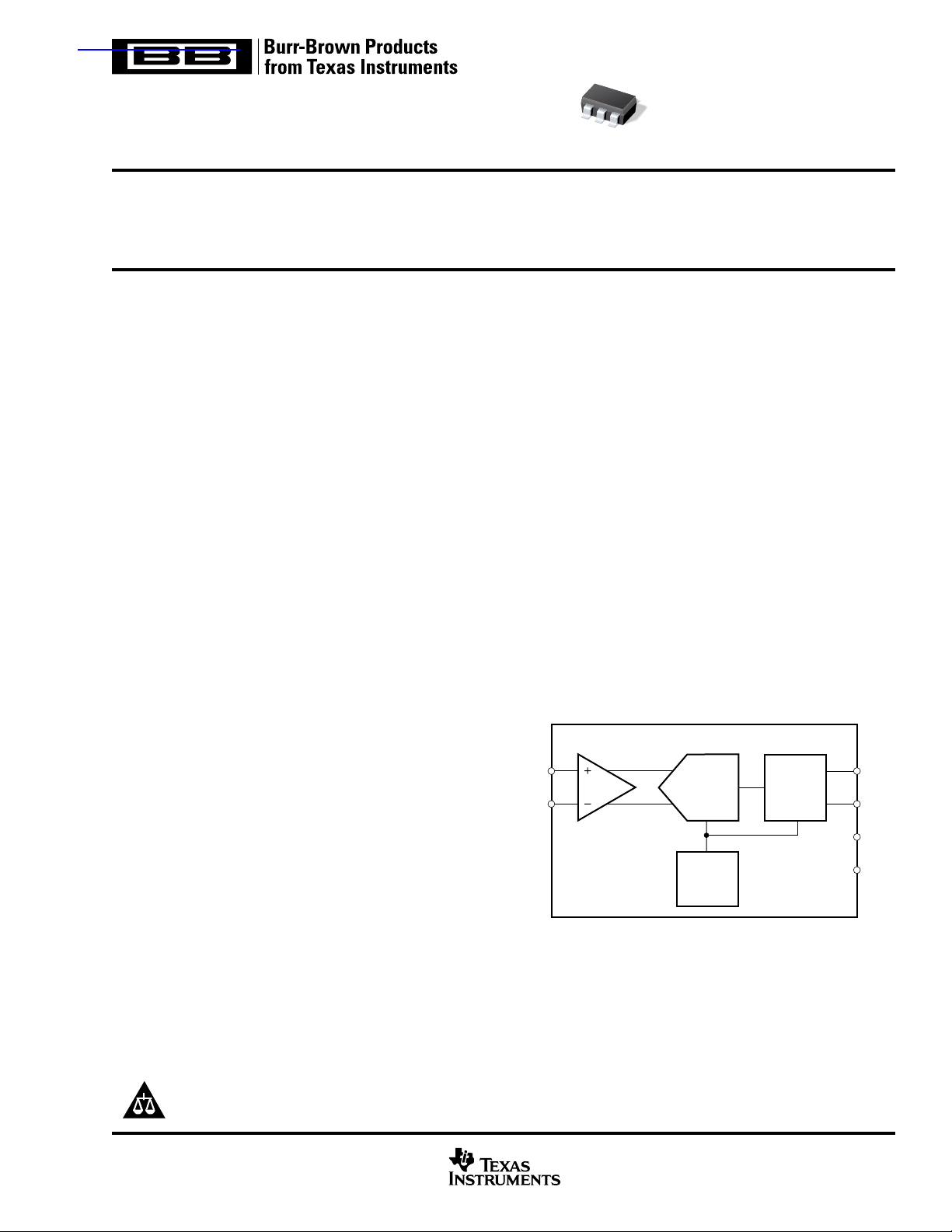
∆Σ A/D
Converter
I2C
Interface
Clock
Oscillator
V
IN+
V
IN–
SCL
SDA
V
DD
GND
A = 1, 2, 4, or 8
PGA
查询ADS1100供应商查询ADS1100供应商
ADS1100
BAAI
SBAS239 – MAY 2002
Self-Calibrating, 16-Bit
ANALOG-TO-DIGITAL CONVERTER
FEATURES
● COMPLETE DATA ACQUISITION SYSTEM IN A
TINY SOT23-6 PACKAGE
● 16-BITS NO MISSING CODES
● INL: 0.0125% of FSR MAX
● CONTINUOUS SELF-CALIBRATION
● SINGLE-CYCLE CONVERSION
● PROGRAMMABLE GAIN AMPLIFIER
GAIN = 1, 2, 4, OR 8
● LOW NOISE: 4
µVp-p
● PROGRAMMABLE DATA RATE: 8SPS to 128SPS
● INTERNAL SYSTEM CLOCK
● I2CTM INTERFACE
● POWER SUPPLY: 2.7V TO 5.5V
● LOW CURRENT CONSUMPTION: 90µA
APPLICATIONS
● PORTABLE INSTRUMENTATION
● INDUSTRIAL PROCESS CONTROL
● SMART TRANSMITTERS
● CONSUMER GOODS
● FACTORY AUTOMATION
● TEMPERATURE MEASUREMENT
DESCRIPTION
The ADS1100 is a precision, continuously self-calibrating
Analog-to-Digital (A/D) converter with differential inputs and
up to 16 bits of resolution in a small SOT23-6 package.
Conversions are performed ratiometrically, using the power
supply as the reference voltage. The ADS1100 uses an
2
I
C-compatible serial interface and operates from a single
power supply ranging from 2.7V to 5.5V.
The ADS1100 can perform conversions at rates of 8, 16, 32,
or 128 samples per second. The onboard programmablegain amplifier, which offers gains of up to 8, allows smaller
signals to be measured with high resolution. In singleconversion mode, the ADS1100 automatically powers down
after a conversion, greatly reducing current consumption
during idle periods.
The ADS1100 is designed for applications requiring highresolution measurement, where space and power consumption are major considerations. Typical applications include
portable instrumentation, industrial process control and smart
transmitters.
I2C is a registered trademark of Philips Incorporated.
PRODUCTION DATA information is current as of publication date.
Products conform to specifications per the terms of Texas Instruments
standard warranty. Production processing does not necessarily include
testing of all parameters.
Please be aware that an important notice concerning availability, standard warranty, and use in critical applications of
Texas Instruments semiconductor products and disclaimers thereto appears at the end of this data sheet.
Copyright © 2002, Texas Instruments Incorporated
www.ti.com
Page 2
ABSOLUTE MAXIMUM RATINGS
VDD to GND ........................................................................... –0.3V to +6V
Input Current ............................................................... 100mA, Momentary
Input Current .................................................................10mA, Continuous
Voltage to GND, V
Voltage to GND, SDA, SCL .....................................................–0.5V to 6V
Maximum Junction Temperature ................................................... +150°C
Operating Temperature .................................................... –40°C to +85°C
Storage Temperature...................................................... –60°C to +150°C
Lead Temperature (soldering, 10s) ............................................... +300°C
NOTE: (1) Stresses above those listed under “Absolute Maximum Ratings” may
cause permanent damage to the device. Exposure to absolute maximum
conditions for extended periods may affect device reliability.
+, VIN–........................................ –0.3V to VDD + 0.3V
IN
This integrated circuit can be damaged by ESD. Texas
Instruments recommends that all integrated circuits be handled
with appropriate precautions. Failure to observe proper handling and installation procedures can cause damage.
ESD damage can range from subtle performance degradation to complete device failure. Precision integrated circuits
may be more susceptible to damage because very small
parametric changes could cause the device not to meet its
ELECTROSTATIC
DISCHARGE SENSITIVITY
published specifications.
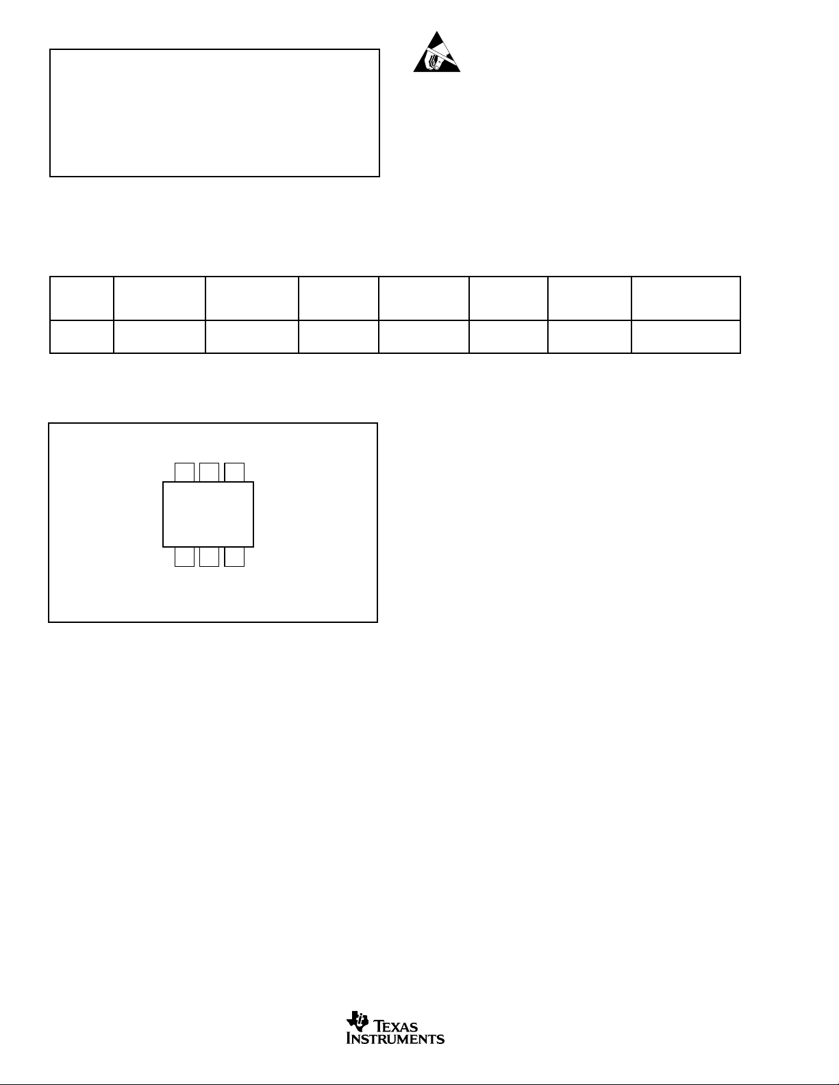
PACKAGE/ORDERING INFORMATION
PRODUCT I
ADS1100 1001 000 SOT23-6 DBV –40°C to +85°C BAAI ADS1100IDBVT Tape and Reel, 250
2
C ADDRESS
(1)
PACKAGE-LEAD DESIGNATOR
PACKAGE TEMPERATURE PACKAGE ORDERING TRANSPORT
"" """"ADS1100IDBVR Tape and Reel, 3000
NOTES: (1) Contact TI or your local sales representative for more information on the availability of other addresses. (2) For the most current specifications and
package information, refer to our web site at www.ti.com.
(2)
SPECIFIED
RANGE MARKING NUMBER MEDIA, QUANTITY
PIN CONFIGURATION
Top View SOT
V
IN–VDD
654
SDA
BAAI
123
GND SCL
V
IN+
NOTE: Marking text direction indicates pin 1.
2
www.ti.com
ADS1100
SBAS239
Page 3

ELECTRICAL CHARACTERISTICS
All specifications at –40°C to +85°C, VDD = 5V, GND = 0V, all PGAs, unless otherwise noted.
ADS1100
PARAMETER CONDITIONS MIN TYP MAX UNITS
ANALOG INPUT
Full-Scale Input Voltage (V
Analog Input Voltage V
Differential Input Impedance 2.4/PGA MΩ
Common-Mode Input Impedance 8MΩ
SYSTEM PERFORMANCE
Resolution and No Missing Codes DR = 00 12 12 Bits
Conversion Rate DR = 00 104 128 184 SPS
Output Noise See Typical Characteristic Curves
Integral Nonlinearity DR = 11, PGA = 1, End Point Fit
Offset Error ±2.5/PGA ±5/PGA mV
Offset Drift PGA = 1 1.5 8 µV/°C
Gain Error 0.01 0.1 %
Gain Error Drift 2 ppm/°C
Common-Mode Rejection At DC, PGA = 8 94 100 dB
DIGITAL INPUT/OUTPUT
Logic Level
V
IH
V
IL
V
OL
Input Leakage
I
IH
I
IL
POWER-SUPPLY REQUIREMENTS
Power-Supply Voltage V
Supply Current Power Down 0.05 2 µA
Power Dissipation
NOTES: (1) 99% of full-scale. (2) FSR = Full-Scale Range = 2 • V
+) – (VIN–) ±VDD/PGA V
IN
+, VIN– to GND GND – 0.2 VDD + 0.2 V
IN
DR = 01 14 14 Bits
DR = 10 15 15 Bits
DR = 11 16 16 Bits
DR = 01 26 32 46 SPS
DR = 10 13 16 23 SPS
DR = 11 6.5 8 11.5 SPS
(1)
±0.003 ±0.0125 % of FSR
PGA = 2 1.0 4 µV/°C
PGA = 4 0.7 2 µV/°C
PGA = 8 0.6 2 µV/°C
At DC, PGA = 1 85 dB
0.7 • V
DD
GND – 0.5 0.3 • V
IOL = 3mA GND 0.4 V
6V
DD
VIH = 5.5V 10 µA
VIL = GND –10 µA
DD
2.7 5.5 V
Active Mode 90 150 µA
V
= 5.0V 450 750 µW
DD
V
= 3.0V 210 µW
DD
/PGA.
DD
(2)
V
ADS1100
SBAS239
www.ti.com
3
Page 4
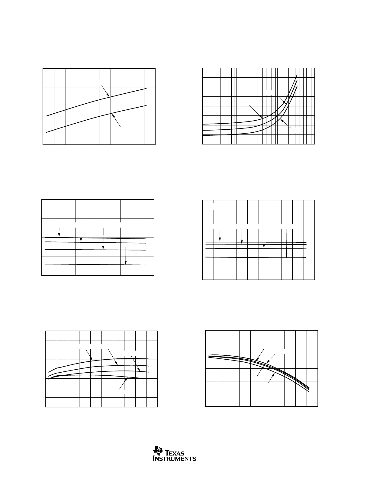
TYPICAL CHARACTERISTICS
At TA = 25°C, VDD = 5V, unless otherwise noted.
120
100
(µA)
80
VDD
I
60
40
–60 –40 –20 0 20 40 60 80 100 120 140
2.0
1.0
0.0
SUPPLY CURRENT vs TEMPERATURE
VDD = 5V
VDD = 2.7V
Temperature (°C)
OFFSET ERROR vs TEMPERATURE
VDD = 5V
PGA = 8 PGA = 4 PGA = 2 PGA = 1
SUPPLY CURRENT vs I2C BUS FREQUENCY
25°C
125°C
10 100 1k 10k
2
I
C Bus Frequency (kHz)
OFFSET ERROR vs TEMPERATURE
(µA)
I
VDD
250
225
200
175
150
125
100
75
50
2.0
VDD = 2.7V
1.0
PGA = 8 PGA = 4 PGA = 2 PGA = 1
0.0
–40°C
Offset Error (mV)
–1.0
–2.0
–60 –40 –20 0 20 40 60 80 100 120 140
Temperature (°C)
0.04
VDD = 5V
0.03
0.02
0.01
0.00
–0.01
Gain Error (%)
–0.02
–0.03
–0.04
–60 –40 –20 0 20 40 60 80 100 120 140
GAIN ERROR vs TEMPERATURE
PGA = 8
PGA = 4
PGA = 1
PGA = 2
Temperature (°C)
Offset Error (mV)
–1.0
–2.0
–60 –40 –20 0 20 40 60 80 100 120 140
Temperature (°C)
0.010
0.005
0.000
–0.005
Gain Error (%)
–0.010
–0.015
–0.020
VDD = 2.7V
–60 –40 –20 0 20 40 60 80 100 120 140
GAIN ERROR vs TEMPERATURE
PGA = 4
PGA = 8
PGA = 1
PGA = 2
Temperature (°C)
4
www.ti.com
ADS1100
SBAS239
Page 5

TYPICAL CHARACTERISTICS
At TA = 25°C, VDD = 5V, unless otherwise noted.
0.0
–0.5
–1.0
–1.5
Total Error (mV)
–2.0
–2.5
–100 –75 –50 –25 0 25 50 75 100
0.05
0.04
0.03
0.02
0.01
Integral Nonlinearity (% of FSR)
0.00
–60 –40 –20 0 20 40 60 80 100 120 140
TOTAL ERROR vs INPUT SIGNAL
PGA = 8
PGA = 4
PGA = 2
PGA = 1
Input Signal (% of Full-Scale)
INTEGRAL NONLINEARITY vs TEMPERATURE
PGA =1
VDD = 2.7V
VDD = 3.5V
Temperature (°C)
Data Rate = 8SPS
VDD = 5V
INTEGRAL NONLINEARITY vs
0.016
0.014
0.012
0.010
0.008
0.006
0.004
0.002
Integral Nonlinearity (% of FSR)
0.000
2.5 3.0 3.5 4.0 4.5 5.0 5.5
20
Data Rate = 8SPS
15
10
5
Noise (p-p, % of LSB)
0
0 20406080100
SUPPLY VOLTAGE
(V)
V
DD
NOISE vs INPUT SIGNAL
PGA = 8
PGA = 4
PGA = 2
PGA = 1
Input Signal (% of Full-Scale)
PGA = 8
PGA = 4
PGA = 2
PGA = 1
30
25
20
15
10
Noise (p-p, % of LSB)
5
Data Rate = 8SPS
0
2.5 3.0 3.5 4.0 4.5 5.0 5.5
NOISE vs SUPPLY VOLTAGE
V
(V)
DD
ADS1100
SBAS239
PGA = 8
PGA = 1
PGA = 4
PGA = 2
www.ti.com
25
Data Rate = 8SPS
PGA = 8
20
15
Noise (p-p, % of LSB)
10
5
–60 –40 –20 0 20 40 60 80 100 120 140
NOISE vs TEMPERATURE
Temperature (°C)
5
Page 6
TYPICAL CHARACTERISTICS
At TA = 25°C, VDD = 5V, unless otherwise noted.
10
9
8
Data Rate (SPS)
7
Data Rate = 8SPS
6
–60 –40 –20 0 20 40 60 80 100 120 140
DATA RATE vs TEMPERATURE
VDD = 2.7V
VDD = 5V
Temperature (°C)
0
Data Rate = 8SPS
–20
–40
Gain (dB)
–60
–80
–100
0.1 1 10 100 1k
FREQUENCY RESPONSE
Input Frequency (Hz)
6
www.ti.com
ADS1100
SBAS239
Page 7

THEORY OF OPERATION
The ADS1100 is a fully differential, 16-bit, self-calibrating,
delta-sigma A/D converter. Extremely easy to design with
and configure, the ADS1100 allows you to take high-quality
measurements with a minimum of effort.
The ADS1100 consists of a delta-sigma A/D converter core
with adjustable gain, a clock generator, and an I
Each of these blocks are described in detail in the sections
that follow.
ANALOG-TO-DIGITAL CONVERTER
The ADS1100’s A/D converter core consists of a differential
switched-capacitor delta-sigma modulator followed by a digital filter. The modulator measures the difference between the
positive and negative analog inputs and compares this to a
reference voltage, which, in the ADS1100, is the power
supply. The digital filter receives a high-speed bitstream from
the modulator and outputs a
code
, which is a number
proportional to the input voltage.
OUTPUT CODE CALCULATION
The output code is a scalar value which is (except for clipping)
proportional to the voltage difference between the two analog
inputs. The output code is confined to a finite range of numbers;
this range depends on the number of bits needed to represent
the code. The number of bits needed to represent the output
code for the ADS1100 depends on the data rate, as shown in
Table I.
Data rate Number of Bits Minimum Code Maximum Code
8SPS 16 –32768 32767
16SPS 15 –16384 16383
32SPS 14 –8192 8191
128SPS 12 –2048 2047
TABLE I. Minimum and Maximum Codes.
For a minimum output code of Min Code, gain setting of
PGA, positive and negative input voltages of V
and power supply of V
, the output code is given by the
DD
expression:
Output Code = –1•Min Code•PGA •
In the above expression, it is important to note that the
negated minimum
output code is used. The ADS1100 out-
V
(
IN
+
2
C interface.
and V
IN+
––V
(
)
IN
V
DD
IN-
)
puts codes in binary two’s complement format, so the absolute values of the minima and maxima are not the same; the
maximum n-bit code is 2
is –1 • 2
n-1
.
n-1
– 1, while the minimum n-bit code
For example, the ideal expression for output codes with a
data rate of 16SPS and PGA = 2 is:
V
––V
Output Code = 16384 • 2•
(
(
)
IN
+
V
DD
The ADS1100 outputs all codes right-justified and signextended. This arrangement makes it possible to perform
averaging on the higher data rate codes using only a 16-bit
accumulator.
Output codes for various input levels are shown in Table II.
SELF-CALIBRATION
The previous expressions for the ADS1100’s output code do
not account for the gain and offset errors in the modulator. To
compensate for these, the ADS1100 incorporates self-calibration circuitry.
The self-calibration system operates continuously, and requires no user intervention. No adjustments can be made to
the self-calibration system, and none need to be made. The
self-calibration system cannot be deactivated.
The offset and gain error figures shown in the specifications
table include the effects of calibration.
CLOCK GENERATOR
The ADS1100 features an onboard clock generator, which
drives the operation of the modulator and digital filter. The
Typical Characteristics show varieties in data rate over
supply voltage and temperature.
It is not possible to operate the ADS1100 with an external
modulator clock.
INPUT IMPEDANCE
The ADS1100 uses a switched-capacitor input stage. To
,
external circuitry, it looks roughly like a resistance. The
resistance value, as with all switched-capacitor circuits, depends on the capacitor values and the rate at which they are
switched. The switching frequency is the same as the modulator frequency; the capacitor values depend on the PGA
setting. The switching clock is generated by the onboard
clock generator, so its frequency, nominally 275 kHz, is
somewhat dependent on supply voltage and temperature.
)
IN
Input Signal
Data Rate Negative Full-Scale –1 LSB Zero +1 LSB Positive Full-Scale
8 SPS 8000
16 SPS C000
32 SPS E000
128 SPS F800
H
H
H
H
FFFF
FFFF
FFFF
FFFF
H
H
H
H
0000
0000
0000
0000
H
H
H
H
0001
0001
0001
0001
H
H
H
H
TABLE II. Output Codes for Different Input Signals.
ADS1100
SBAS239
www.ti.com
7FFF
3FFF
1FFF
07FF
H
H
H
H
7
Page 8

The common-mode and differential input impedances are
different. For a gain setting of PGA, the differential input
impedance is typically:
2.4MΩ / PGA
The common mode impedance is typically 8MΩ.
The typical value of the input impedance often cannot be
neglected. Unless the input source has a low impedance, the
ADS1100’s input impedance may affect the measurement
accuracy. For sources with high output impedance, buffering
may be necessary. Bear in mind, however, that active buffers
introduce noise, and also introduce offset and gain errors. All
of these factors should be considered in high-accuracy
applications.
Because the clock generator frequency drifts slightly with
temperature, the input impedances will also drift. For many
applications, this input impedance drift can be neglected, and
the typical impedance values above can be used.
ALIASING
If frequencies are input to the ADS1100 which exceed half
the data rate, aliasing will occur. To prevent aliasing, the
input signal must be bandlimited. Some signals are inherently bandlimited, for example, a thermocouple’s output,
which has a limited rate of change, but may nevertheless
contain noise and interference components. These can fold
back into the sampling band just as any other signal can.
The ADS1100’s digital filter provides some attenuation of
high frequency noise, but the filter’s sinc
1
frequency response cannot completely replace an anti-aliasing filter;
some external filtering may still be needed. For many applications, a simple RC filter will suffice.
When designing an input filter circuit, remember to take the
interaction between the filter network and the input impedance of the ADS1100 into account.
USING THE ADS1100
OPERATING MODES
The ADS1100 operates in one of two modes:
conversion
and
single conversion.
In continuous conversion mode, the ADS1100 continuously
performs conversions. Once a conversion has been completed, the ADS1100 places the result in the output register,
and immediately begins another conversion. When the
ADS1100 is in continuous conversion mode, the ST/BSY bit
in the configuration register always reads 1.
In single conversion mode, the ADS1100 waits until the
ST/BSY bit in the conversion register is set to 1. When this
happens, the ADS1100 powers up and performs a single
conversion. After the conversion completes, the ADS1100
places the result in the output register, resets the ST/BSY bit
to 0 and powers down. Writing a 1 to ST/BSY while a
conversion is in progress has no effect.
When switching from continuous conversion mode to single
conversion mode, the ADS1100 will complete the current
conversion, reset the ST/BSY bit to 0 and power down.
continuous
RESET AND POWER-UP
When the ADS1100 powers up, it automatically performs a
reset. As part of the reset, the ADS1100 sets all of the bits
in the configuration register to their default setting.
The ADS1100 responds to the I
2
C General Call Reset
command. When the ADS1100 receives a General Call
Reset, it performs an internal reset, exactly as though it had
just been powered on.
2
I
C INTERFACE
2
The ADS1100 communicates through an I
grated Circuit) interface. The I
2
C interface is a 2-wire open-
C (Inter-Inte-
drain interface supporting multiple devices and masters on a
single bus. Devices on the I
2
C bus only drive the bus lines
LOW, by connecting them to ground; they never drive the
bus lines HIGH. Instead, the bus wires are pulled HIGH by
pull-up resistors, so the bus wires are HIGH when no device
is driving them LOW. This way, two devices cannot conflict;
if two devices drive the bus simultaneously, there is no driver
contention.
Communication on the I
two devices, one acting as the
as the
slave.
Both masters and slaves can read and write,
2
C bus always takes place between
master
and the other acting
but slaves can only do so under the direction of the master.
Some I
2
C devices can act as masters or slaves, but the
ADS1100 can only act as a slave device.
An I2C bus consists of two lines, SDA and SCL. SDA carries
data; SCL provides the clock. All data is transmitted across
2
the I
C bus in groups of eight bits. To send a bit on the I2C
bus, the SDA line is driven to the bit’s level while SCL is
LOW. (A LOW on SDA indicates a zero bit; a HIGH indicates
a one bit.) Once the SDA line has settled, the SCL line is
brought HIGH, then LOW. This pulse on SCL clocks the SDA
bit into the receiver’s shift register.
2
The I
C bus is bidirectional: the SDA line is used both for
transmitting and receiving data. When a master reads from
a slave, the slave drives the data line; when a master sends
to a slave, the master drives the data line. The master always
drives the clock line. The ADS1100 never drives SCL,
because it cannot act as a master. On the ADS1100, SCL is
an input only.
Most of the time the bus is
idle,
no communication is taking
place, and both lines are HIGH. When communication is
taking place, the bus is
a communication. They do this by causing a
active
. Only master devices can start
start condition
on the bus. Normally, the data line is only allowed to change
state while the clock line is LOW. If the data line changes
state while the clock line is HIGH, it is either a
or its counterpart, a
stop condition.
A start condition is when
start condition
the clock line is HIGH and the data line goes from HIGH to
LOW. A stop condition is when the clock line is HIGH and the
data line goes from LOW to HIGH.
After the master issues a start condition, it sends a byte
which indicates which slave device it wants to communicate
with. This byte is called the
2
I
C bus has a unique 7-bit address to which it responds.
(Slaves can also have 10-bit addresses; see the I
address byte.
Each device on an
2
C specifi-
8
www.ti.com
ADS1100
SBAS239
Page 9

cation for details.) The master sends an address in the
address byte, together with a bit which indicates whether it
wishes to read from or write to the slave device.
Every byte transmitted on the I
or data, is acknowledged with an
2
C bus, whether it be address
acknowledge bit.
When a
master has finished sending a byte, eight data bits, to a
slave, it stops driving SDA and waits for the slave to acknowledge the byte. The slave acknowledges the byte by pulling
SDA LOW. The master then sends a clock pulse to clock the
acknowledge bit. Similarly, when a master has finished
reading a byte, it pulls SDA LOW to acknowledge this to the
slave. It then sends a clock pulse to clock the bit. (Remember
that the master
always
drives the clock line.)
A not-acknowledge is performed by simply leaving SDA
HIGH during an acknowledge cycle. If a device is not present
on the bus, and the master attempts to address it, it will
receive a not-acknowledge because no device is present at
that address to pull the line LOW.
When a master has finished communicating with a slave, it
may issue a stop condition. When a stop condition is issued,
the bus becomes idle again. A master may also issue
another start condition. When a start condition is issued while
the bus is active, it is called a
repeated start condition.
A timing diagram for an ADS1100 I2C transaction is shown in
Figure 1. Table III gives the parameters for this diagram.
ADS1100 I2C ADDRESS
2
The ADS1100’s I
C address is 1001
set at the factory. The ADS1100 is shipped with
aaa
, where
aaa
aaa
are bits
set to
zero, so its address is 1001000.
Contact Texas Instruments for information about the avail-
ability of other addresses.
2
I
C GENERAL CALL
The ADS1100 responds to General Call Reset, which is an
address byte of 00H followed by a data byte of 06H. The
ADS1100 acknowledges both bytes.
On receiving a General Call Reset, the ADS1100 performs a
full internal reset, just as though it had been powered off and
then on. If a conversion is in process, it is interrupted; the
output register is set to zero; and the configuration register is
set to its default setting.
The ADS1100 always acknowledges the General Call address byte of 00
Call data bytes other than 04
, but it does not acknowledge any General
H
or 06H.
H
I2C DATA RATES
2
C bus operates in one of three speed modes: Stan-
The I
dard, which allows a clock frequency of up to 100kHz; Fast,
which allows a clock frequency of up to 400kHz; and High-
t
SCL
SDA
(LOW)
t
(HDSTA)
t
(BUF)
PS S P
t
R
t
(HDDAT)
t
F
t
(HIGH)
t
(SUSTA)
t
(SUDAT)
t
(HDSTA)
t
(SUSTO)
FIGURE 1. I2C Timing Diagram.
FAST MODE HIGH-SPEED MODE
PARAMETER MIN MAX MIN MAX UNITS
SCLK Operating Frequency f
Bus Free Time Between STOP and START Condition t
Hold Time After Repeated START Condition. t
After this period, the first clock is generated.
Repeated START Condition Setup Time t
STOP Condition Setup Time t
Data Hold Time t
Data Setup Time t
SCLK Clock LOW Period t
SCLK Clock HIGH Period t
Clock/Data Fall Time t
Clock/Data Rise Time t
(SCLK)
(BUF)
(HDSTA)
(SUSTA)
(SUSTO)
(HDDAT)
(SUDAT)
(LOW)
(HIGH)
600 160 ns
600 160 ns
600 160 ns
600 160 ns
00ns
100 10 ns
1300 160 ns
600 60 ns
F
R
0.4 3.4 MHz
300 160 ns
300 160 ns
TABLE III. Timing Diagram Definitions.
ADS1100
SBAS239
www.ti.com
9
Page 10

speed mode (also called Hs mode), which allows a clock
frequency of up to 3.4MHz. The ADS1100 is fully compatible
with all three modes.
No special action needs to be taken to use the ADS1100 in
Standard or Fast modes, but High-speed mode must be
activated. To activate High-speed mode, send a special
address byte of 00001XXX following the start condition,
where the XXX bits are unique to the Hs-capable master.
This byte is called the Hs master code. (Note that this is
different from normal address bytes: the low bit does not
indicate read/write status.) The ADS1100 will not acknowledge this byte; the I
2
C specification prohibits acknowledgment of the Hs master code. On receiving a master code, the
ADS1100 will switch on its High-speed mode filters, and will
communicate at up to 3.4MHz. The ADS1100 switches out of
Hs mode with the next stop condition.
For more information on High-speed mode, consult the I
2
specification.
In continuous conversion mode, the ADS1100 ignores the
value written to ST/BSY.
When read in single conversion mode, ST/BSY indicates
whether the A/D converter is busy taking a conversion. If ST/
BSY is read as 1, the A/D converter is busy, and a conversion
is taking place; if 0, no conversion is taking place, and the
result of the last conversion is available in the output register.
In continuous mode, ST/BSY is always read as 1.
Bits 6-5: Reserved
Bits 6 and 5 must be set to zero.
Bit 4: SC
SC controls whether the ADS1100 is in continuous conversion or single conversion mode. When SC is 1, the ADS1100
C
is in single conversion mode; when SC is 0, the ADS1100 is
in continuous conversion mode. The default setting is 0.
REGISTERS
The ADS1100 has two registers which are accessible via its
2
I
C port. The
conversion; the
output register
contains the result of the last
configuration register
allows you to change
the ADS1100’s operating mode and query the status of the
device.
OUTPUT REGISTER
The 16-bit output register contains the result of the last
conversion in binary two’s complement format. Following
reset or power-up, the output register is cleared to zero; it
remains zero until the first conversion is completed. Therefore, if you read the ADS1100 just after reset or power-up,
you will read zero from the output register.
The output register’s format is shown in Table V.
CONFIGURATION REGISTER
You can use the 8-bit configuration register to control the
ADS1100’s operating mode, data rate, and PGA settings.
The configuration register’s format is shown in Table IV. The
default setting is 8CH.
BIT 7 654321 0
NAME ST/BSY 0 0 SC DR1 DR0 PGA1 PGA0
TABLE IV. Configuration Register.
Bit 7: ST/BSY
The meaning of the ST/BSY bit depends on whether it is
being written to or read from.
In single conversion mode, writing a 1 to the ST/BSY bit
causes a conversion to start, and writing a 0 has no effect.
Bits 3-2: DR
Bits 3 and 2 control the ADS1100’s data rate, as shown in
Table VI.
DR1 DR0 DATA RATE
0 0 128SPS
0 1 32SPS
1 0 16SPS
(1)
1
NOTE: (1) Default Setting
(1)
1
8SPS
(1)
TABLE VI. DR Bits.
Bits 1-0: PGA
Bits 1 and 0 control the ADS1100’s gain setting, as shown in
Table VII.
PGA1 PGA0 GAIN
(1)
0
01 2
10 4
11 8
NOTE: (1) Default Setting.
(1)
0
(1)
1
TABLE VII. PGA Bits.
READING FROM THE ADS1100
You can read the output register and the contents of the
configuration register from the ADS1100. To do this, address
the ADS1100 for reading, and read three bytes from the
device. The first two bytes are the output register’s contents;
the third byte is the configuration register’s contents.
You do not always have to read three bytes from the
ADS1100. If you want only the contents of the output register, read only two bytes.
BIT 1514131211109876543210
NAME D15D14D13D12D11D10D9D8D7D6D5D4D3D2D1D0
TABLE V. Output Register.
10
www.ti.com
ADS1100
SBAS239
Page 11

Reading more than three bytes from the ADS1100 has no
Frame 1: I2C Slave Address Byte Frame 2: Output Register Upper Byte
Start By
Master
ACK By
ADS1100
ACK By
Master
From
ADS1100
From
ADS1100
191
9
…
…
…
…
SDA
SCL
SDA
(Continued)
SCL
(Continued)
1 0 0 1 A2 A1 A0 R/W
D15 D14 D13 D12 D11 D10 D9 D8
Frame 3: Output Register Lower Byte Frame 4: Configuration Register
(Optional)
ACK By
Master
Stop By
Master
ACK By
Master
From
ADS1100
1
91
D7 D6 D5 D4 D3 D2 D1 D0
ST/
BSY
0 0 SC DR1 DR0
PGA1 PGA0
9
effect. All of the bytes beginning with the fourth will be FF
H
A timing diagram for an ADS1100 read operation is shown in
Figure 2.
WRITING TO THE ADS1100
You can write new contents into the configuration register
(you cannot change the contents of the output register). To
do this, address the ADS1100 for writing, and write one byte
.
to it. This byte is written into the configuration register.
Writing more than one byte to the ADS1100 has no effect.
The ADS1100 will ignore any bytes sent to it after the first
one, and it will only acknowledge the first byte.
A timing diagram for an ADS1100 write operation is shown in
Figure 3.
FIGURE 2. Timing Diagram for Reading From the ADS1100.
1919
SCL
SDA
Start By
Master
001A2A1 A0 R/W
1
Frame 1: I2C Slave Address Byte Frame 2: Configuration Register
FIGURE 3. Timing Diagram for Writing to the ADS1100.
ADS1100
SBAS239
ST/
0 0 SC DR1 DR0
BSY
ACK By
ADS1100
www.ti.com
PGA1 PGA0
ACK By
ADS1100
Stop By
Master
11
Page 12

PACKAGE DRAWING
MPDS026D – FEBRUARY 1997 – REVISED FEBRUARY 2002
DBV (R-PDSO-G6) PLASTIC SMALL-OUTLINE
0,95
1,45
0,95
3,00
2,80
46
31
0,05 MIN
6X
0,50
0,25
1,70
1,50
0,20
3,00
2,60
Seating Plane
M
0,15 NOM
Gage Plane
0,25
0–8
0,10
0,55
0,35
NOTES: A. All linear dimensions are in millimeters.
B. This drawing is subject to change without notice.
C. Body dimensions do not include mold flash or protrusion.
D. Leads 1, 2, 3 may be wider than leads 4, 5, 6 for package orientation.
4073253-5/G 01/02
12
www.ti.com
ADS1100
SBAS239
Page 13

IMPORTANT NOTICE
Texas Instruments Incorporated and its subsidiaries (TI) reserve the right to make corrections, modifications,
enhancements, improvements, and other changes to its products and services at any time and to discontinue
any product or service without notice. Customers should obtain the latest relevant information before placing
orders and should verify that such information is current and complete. All products are sold subject to TI’s terms
and conditions of sale supplied at the time of order acknowledgment.
TI warrants performance of its hardware products to the specifications applicable at the time of sale in
accordance with TI’s standard warranty . Testing and other quality control techniques are used to the extent TI
deems necessary to support this warranty . Except where mandated by government requirements, testing of all
parameters of each product is not necessarily performed.
TI assumes no liability for applications assistance or customer product design. Customers are responsible for
their products and applications using TI components. T o minimize the risks associated with customer products
and applications, customers should provide adequate design and operating safeguards.
TI does not warrant or represent that any license, either express or implied, is granted under any TI patent right,
copyright, mask work right, or other TI intellectual property right relating to any combination, machine, or process
in which TI products or services are used. Information published by TI regarding third–party products or services
does not constitute a license from TI to use such products or services or a warranty or endorsement thereof.
Use of such information may require a license from a third party under the patents or other intellectual property
of the third party , or a license from TI under the patents or other intellectual property of TI.
Reproduction of information in TI data books or data sheets is permissible only if reproduction is without
alteration and is accompanied by all associated warranties, conditions, limitations, and notices. Reproduction
of this information with alteration is an unfair and deceptive business practice. TI is not responsible or liable for
such altered documentation.
Resale of TI products or services with statements different from or beyond the parameters stated by TI for that
product or service voids all express and any implied warranties for the associated TI product or service and
is an unfair and deceptive business practice. TI is not responsible or liable for any such statements.
Mailing Address:
Texas Instruments
Post Office Box 655303
Dallas, Texas 75265
Copyright 2002, Texas Instruments Incorporated
 Loading...