

Page 1
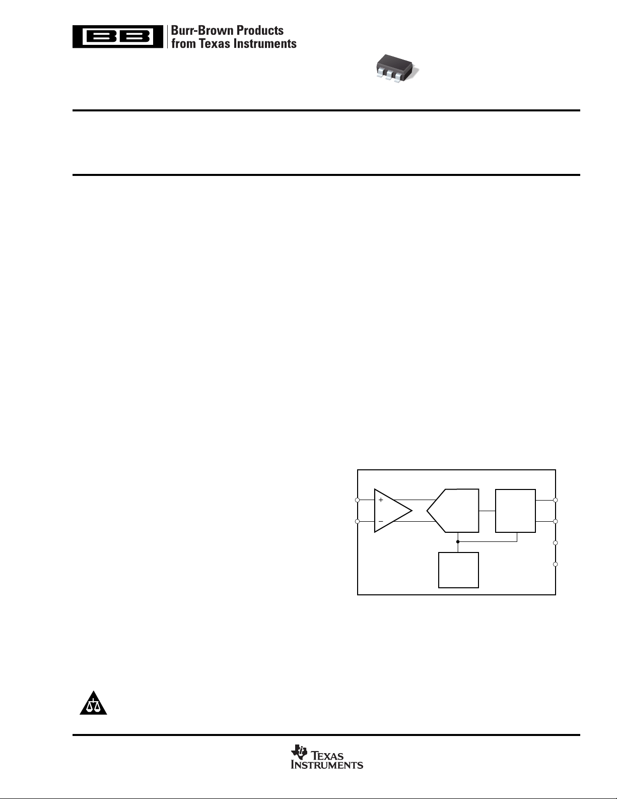
∆Σ A/D
Converter
I2C
Interface
Clock
Oscillator
V
IN+
V
IN–
SCL
SDA
V
DD
GND
A = 1, 2, 4, or 8
PGA
AD0
SBAS239B – MAY 2002 – REVISED NOVEMBER 2003
Self-Calibrating, 16-Bit
ANALOG-TO-DIGITAL CONVERTER
ADS1100
FEATURES
● COMPLETE DATA ACQUISITION SYSTEM IN A
TINY SOT23-6 PACKAGE
● 16-BITS NO MISSING CODES
● INL: 0.0125% of FSR MAX
● CONTINUOUS SELF-CALIBRATION
● SINGLE-CYCLE CONVERSION
● PROGRAMMABLE GAIN AMPLIFIER
GAIN = 1, 2, 4, OR 8
● LOW NOISE: 4
µVp-p
● PROGRAMMABLE DATA RATE: 8SPS to 128SPS
● INTERNAL SYSTEM CLOCK
● I2CTM INTERFACE
● POWER SUPPLY: 2.7V to 5.5V
● LOW CURRENT CONSUMPTION: 90µA
● AVAILABLE IN EIGHT DIFFERENT ADDRESSES
APPLICATIONS
● PORTABLE INSTRUMENTATION
● INDUSTRIAL PROCESS CONTROL
● SMART TRANSMITTERS
● CONSUMER GOODS
● FACTORY AUTOMATION
● TEMPERATURE MEASUREMENT
I2C is a registered trademark of Philips Incorporated.
DESCRIPTION
The ADS1100 is a precision, continuously self-calibrating
Analog-to-Digital (A/D) converter with differential inputs and
up to 16 bits of resolution in a small SOT23-6 package.
Conversions are performed ratiometrically, using the power
supply as the reference voltage. The ADS1100 uses an
2
I
C-compatible serial interface and operates from a single
power supply ranging from 2.7V to 5.5V.
The ADS1100 can perform conversions at rates of 8, 16, 32,
or 128 samples per second. The onboard Programmable
Gain Amplifier (PGA), which offers gains of up to 8, allows
smaller signals to be measured with high resolution. In
single-conversion mode, the ADS1100 automatically powers
down after a conversion, greatly reducing current consumption during idle periods.
The ADS1100 is designed for applications requiring highresolution measurement, where space and power consumption are major considerations. Typical applications include
portable instrumentation, industrial process control, and smart
transmitters.
All trademarks are the property of their respective owners.
PRODUCTION DATA information is current as of publication date.
Products conform to specifications per the terms of Texas Instruments
standard warranty. Production processing does not necessarily include
testing of all parameters.
Please be aware that an important notice concerning availability, standard warranty, and use in critical applications of
Texas Instruments semiconductor products and disclaimers thereto appears at the end of this data sheet.
Copyright © 2002-2003, Texas Instruments Incorporated
www.ti.com
Page 2
ABSOLUTE MAXIMUM RATINGS
VDD to GND ........................................................................... –0.3V to +6V
Input Current ............................................................... 100mA, Momentary
Input Current .................................................................10mA, Continuous
, V
Voltage to GND, V
Voltage to GND, SDA, SCL .....................................................–0.5V to 6V
Maximum Junction Temperature ................................................... +150°C
Operating Temperature .................................................. –40°C to +125°C
Storage Temperature...................................................... –60°C to +150°C
Lead Temperature (soldering, 10s) ............................................... +300°C
NOTE: (1) Stresses above those listed under “Absolute Maximum Ratings” may
cause permanent damage to the device. Exposure to absolute maximum
conditions for extended periods may affect device reliability.
.......................................................... –0.3V to V
IN+
IN–
DD
+ 0.3V
This integrated circuit can be damaged by ESD. Texas
Instruments recommends that all integrated circuits be handled
with appropriate precautions. Failure to observe proper handling and installation procedures can cause damage.
ESD damage can range from subtle performance degradation to complete device failure. Precision integrated circuits
may be more susceptible to damage because very small
parametric changes could cause the device not to meet its
ELECTROSTATIC
DISCHARGE SENSITIVITY
published specifications.
PACKAGE/ORDERING INFORMATION
PRODUCT I
ADS1100 1001 000 SOT23-6 DBV –40°C to +85°C AD0 ADS1100A0IDBVT Tape and Reel, 250
2
C ADDRESS PACKAGE-LEAD DESIGNATOR
PACKAGE TEMPERATURE PACKAGE ORDERING TRANSPORT
"" " " " "ADS1100A0IDBVR Tape and Reel, 3000
ADS1100 1001 001 SOT23-6 DBV –40°C to +85°C AD1 ADS1100A1IDBVT Tape and Reel, 250
"" " " " "ADS1100A1IDBVR Tape and Reel, 3000
ADS1100 1001 010 SOT23-6 DBV –40°C to +85°C AD2 ADS1100A2IDBVT Tape and Reel, 250
"" " " " "ADS1100A2IDBVR Tape and Reel, 3000
ADS1100 1001 011 SOT23-6 DBV –40°C to +85°C AD3 ADS1100A3IDBVT Tape and Reel, 250
"" " " " "ADS1100A3IDBVR Tape and Reel, 3000
ADS1100 1001 100 SOT23-6 DBV –40°C to +85°C AD4 ADS1100A4IDBVT Tape and Reel, 250
"" " " " "ADS1100A4IDBVR Tape and Reel, 3000
ADS1100 1001 101 SOT23-6 DBV –40°C to +85°C AD5 ADS1100A5IDBVT Tape and Reel, 250
"" " " " "ADS1100A5IDBVR Tape and Reel, 3000
ADS1100 1001 110 SOT23-6 DBV –40°C to +85°C AD6 ADS1100A6IDBVT Tape and Reel, 250
"" " " " "ADS1100A6IDBVR Tape and Reel, 3000
ADS1100 1001 111 SOT23-6 DBV –40°C to +85°C AD7 ADS1100A7IDBVT Tape and Reel, 250
"" " " " "ADS1100A7IDBVR Tape and Reel, 3000
NOTE: (1) For the most current specifications and package information, refer to our web site at www.ti.com.
(1)
SPECIFIED
RANGE MARKING NUMBER MEDIA, QUANTITY
PIN CONFIGURATION
Top View SOT23
V
IN–VDD
654
SDA
AD0
123
GND SCL
V
IN+
NOTE: Marking text direction indicates pin 1. Marking text depends on I2C
address; see ordering table. Marking for I
2
C address 1001000 shown.
2
www.ti.com
ADS1100
SBAS239B
Page 3

ELECTRICAL CHARACTERISTICS
All specifications at –40°C to +85°C, VDD = 5V, GND = 0V, and all PGAs, unless otherwise noted.
ADS1100
PARAMETER CONDITIONS MIN TYP MAX UNITS
ANALOG INPUT
Full-Scale Input Voltage (V
Analog Input Voltage V
Differential Input Impedance 2.4/PGA MΩ
Common-Mode Input Impedance 8MΩ
SYSTEM PERFORMANCE
Resolution and No Missing Codes DR = 00 12 12 Bits
Conversion Rate DR = 00 104 128 184 SPS
Output Noise See Typical Characteristic Curves
Integral Nonlinearity DR = 11, PGA = 1, End Point Fit
Offset Error ±2.5/PGA ±5/PGA mV
Offset Drift PGA = 1 1.5 8 µV/°C
Gain Error 0.01 0.1 %
Gain Error Drift 2 ppm/°C
Common-Mode Rejection At DC, PGA = 8 94 100 dB
DIGITAL INPUT/OUTPUT
Logic Level
V
IH
V
IL
V
OL
Input Leakage
I
IH
I
IL
POWER-SUPPLY REQUIREMENTS
Power-Supply Voltage V
Supply Current Power Down 0.05 2 µA
Power Dissipation
NOTES: (1) 99% of full-scale. (2) FSR = Full-Scale Range = 2 • V
) – (V
IN+
, V
IN+
) ±VDD/PGA V
IN–
to GND GND – 0.2 VDD + 0.2 V
IN–
DR = 01 14 14 Bits
DR = 10 15 15 Bits
DR = 11 16 16 Bits
DR = 01 26 32 46 SPS
DR = 10 13 16 23 SPS
DR = 11 6.5 8 11.5 SPS
(1)
±0.003 ±0.0125 % of FSR
PGA = 2 1.0 4 µV/°C
PGA = 4 0.7 2 µV/°C
PGA = 8 0.6 2 µV/°C
At DC, PGA = 1 85 dB
0.7 • V
DD
GND – 0.5 0.3 • V
IOL = 3mA GND 0.4 V
6V
DD
VIH = 5.5V 10 µA
VIL = GND –10 µA
DD
2.7 5.5 V
Active Mode 90 150 µA
V
= 5.0V 450 750 µW
DD
V
= 3.0V 210 µW
DD
/PGA.
DD
(2)
V
ADS1100
SBAS239B
www.ti.com
3
Page 4
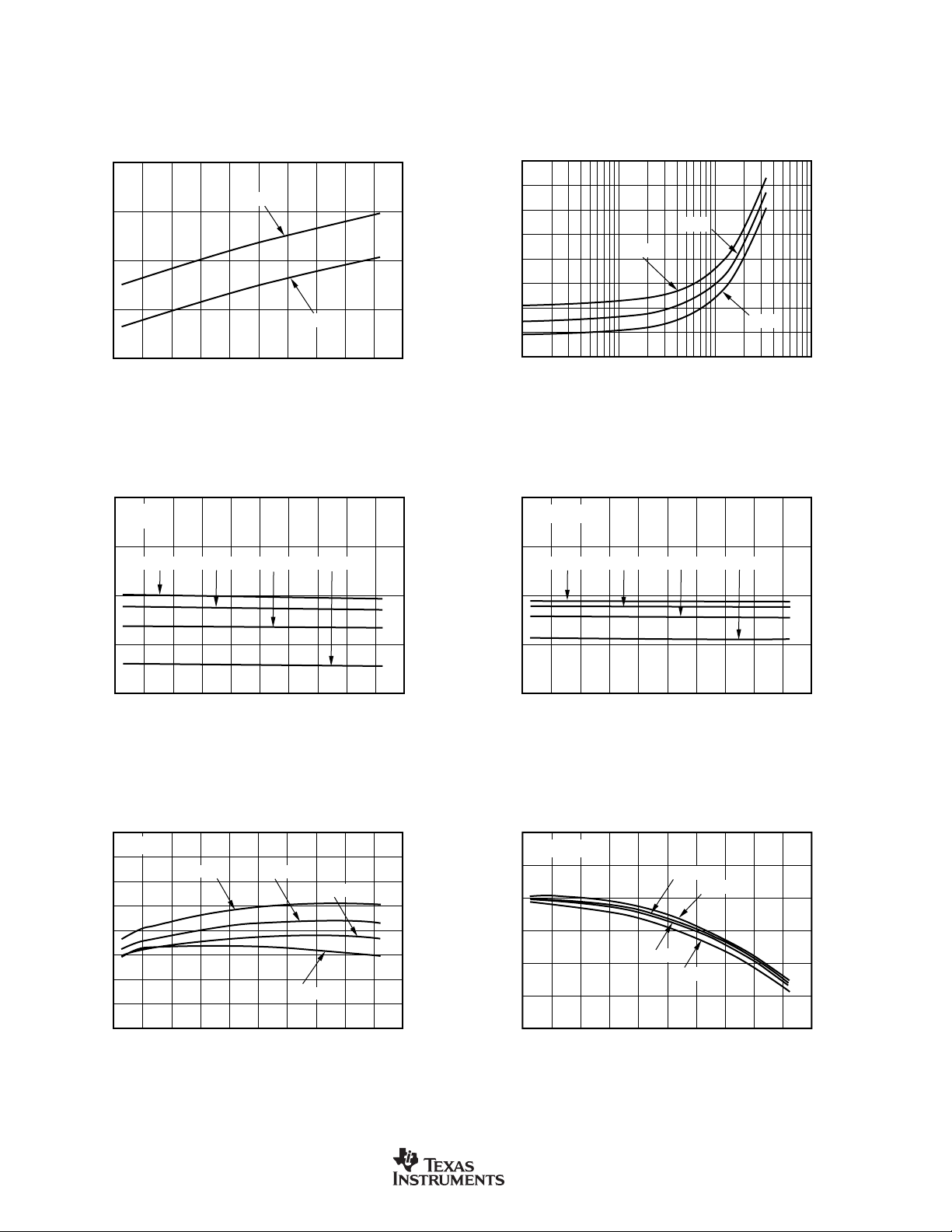
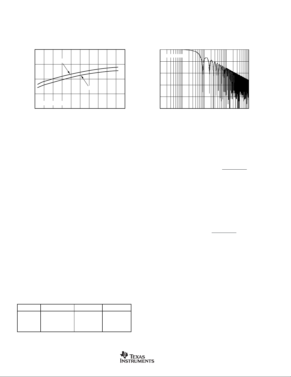
TYPICAL CHARACTERISTICS
At TA = 25°C and VDD = 5V, unless otherwise noted.
120
100
(µA)
80
VDD
I
60
40
–60 –40 –20 0 20 40 60 80 100 120 140
2.0
1.0
0.0
SUPPLY CURRENT vs TEMPERATURE
VDD = 5V
VDD = 2.7V
Temperature (°C)
OFFSET ERROR vs TEMPERATURE
VDD = 5V
PGA = 8 PGA = 4 PGA = 2 PGA = 1
SUPPLY CURRENT vs I2C BUS FREQUENCY
25°C
125°C
10 100 1k 10k
VDD = 2.7V
PGA = 8 PGA = 4 PGA = 2 PGA = 1
2
I
C Bus Frequency (kHz)
OFFSET ERROR vs TEMPERATURE
(µA)
I
VDD
250
225
200
175
150
125
100
75
50
2.0
1.0
0.0
–40°C
Offset Error (mV)
–1.0
–2.0
–60 –40 –20 0 20 40 60 80 100 120 140
Temperature (°C)
0.04
VDD = 5V
0.03
0.02
0.01
0.00
–0.01
Gain Error (%)
–0.02
–0.03
–0.04
–60 –40 –20 0 20 40 60 80 100 120 140
GAIN ERROR vs TEMPERATURE
PGA = 8
Temperature (°C)
PGA = 4
PGA = 1
PGA = 2
Offset Error (mV)
–1.0
–2.0
–60 –40 –20 0 20 40 60 80 100 120 140
Temperature (°C)
0.010
0.005
0.000
–0.005
Gain Error (%)
–0.010
–0.015
–0.020
VDD = 2.7V
–60 –40 –20 0 20 40 60 80 100 120 140
GAIN ERROR vs TEMPERATURE
PGA = 4
PGA = 8
PGA = 1
PGA = 2
Temperature (°C)
4
www.ti.com
ADS1100
SBAS239B
Page 5
TYPICAL CHARACTERISTICS (Cont.)
NOISE vs TEMPERATURE
25
20
15
10
5
Noise (p-p, % of LSB)
–60 –40 –20 0 20 40 60 80 100 120 140
Temperature (°C)
Data Rate = 8SPS
PGA = 8
At TA = 25°C and VDD = 5V, unless otherwise noted.
0.0
–0.5
–1.0
–1.5
Total Error (mV)
–2.0
–2.5
–100 –75 –50 –25 0 25 50 75 100
0.05
PGA =1
0.04
0.03
0.02
0.01
Integral Nonlinearity (% of FSR)
0.00
–60 –40 –20 0 20 40 60 80 100 120 140
TOTAL ERROR vs INPUT SIGNAL
PGA = 8
PGA = 4
PGA = 2
PGA = 1
Input Signal (% of Full-Scale)
INTEGRAL NONLINEARITY vs TEMPERATURE
VDD = 2.7V
VDD = 3.5V
Temperature (°C)
Data Rate = 8SPS
VDD = 5V
0.016
0.014
0.012
0.010
0.008
0.006
0.004
0.002
Integral Nonlinearity (% of FSR)
0.000
Noise (p-p, % of LSB)
INTEGRAL NONLINEARITY vs SUPPLY VOLTAGE
2.5 3.0 3.5 4.0 4.5 5.0 5.5
(V)
V
DD
20
Data Rate = 8SPS
15
10
5
0
0 20406080100
NOISE vs INPUT SIGNAL
PGA = 8
PGA = 4
PGA = 2
PGA = 1
Input Signal (% of Full-Scale)
PGA = 8
PGA = 4
PGA = 2
PGA = 1
NOISE vs SUPPLY VOLTAGE
30
25
20
15
10
Noise (p-p, % of LSB)
5
Data Rate = 8SPS
0
2.5 3.0 3.5 4.0 4.5 5.0 5.5
ADS1100
SBAS239B
PGA = 8
PGA = 4
PGA = 2
PGA = 1
V
(V)
DD
www.ti.com
5
Page 6
TYPICAL CHARACTERISTICS (Cont.)
At TA = 25°C and VDD = 5V, unless otherwise noted.
10
9
8
Data Rate (SPS)
7
Data Rate = 8SPS
6
–60 –40 –20 0 20 40 60 80 100 120 140
DATA RATE vs TEMPERATURE
VDD = 2.7V
VDD = 5V
Temperature (°C)
THEORY OF OPERATION
The ADS1100 is a fully differential, 16-bit, self-calibrating,
delta-sigma A/D converter. Extremely easy to design with
and configure, the ADS1100 allows you to obtain precise
measurements with a minimum of effort.
The ADS1100 consists of a delta-sigma A/D converter core with
adjustable gain, a clock generator, and an I
these blocks are described in detail in the sections that follow.
ANALOG-TO-DIGITAL CONVERTER
The ADS1100 A/D converter core consists of a differential
switched-capacitor delta-sigma modulator followed by a digital
filter. The modulator measures the voltage difference between
the positive and negative analog inputs and compares it to a
reference voltage, which, in the ADS1100, is the power
supply. The digital filter receives a high-speed bitstream from
the modulator and outputs a code, which is a number
proportional to the input voltage.
OUTPUT CODE CALCULATION
The output code is a scalar value that is (except for clipping)
proportional to the voltage difference between the two analog
inputs. The output code is confined to a finite range of numbers;
this range depends on the number of bits needed to represent the
code. The number of bits needed to represent the output code for
the ADS1100 depends on the data rate, as shown in Table I.
DATA RATE NUMBER OF BITS MINIMUM CODE MAXIMUM CODE
8SPS 16 –32,768 32,767
16SPS 15 –16,384 16,383
32SPS 14 –8192 8191
128SPS 12 –2048 2047
TABLE I. Minimum and Maximum Codes.
2
C interface. Each of
0
Data Rate = 8SPS
–20
–40
Gain (dB)
–60
–80
–100
0.1 1 10 100 1k
FREQUENCY RESPONSE
Input Frequency (Hz)
For a minimum output code of Min Code, gain setting of
PGA, positive and negative input voltages of V
and power supply of V
, the output code is given by the
DD
IN+
and V
IN–
expression:
––V
V
(
(
)
IN
Output Code = –1•Min Code•PGA •
+
In the previous expression, it is important to note that the
minimum
output code is used. The ADS1100 outputs codes in
V
DD
)
IN
negated
binary two’s complement format, so the absolute values of the
minima and maxima are not the same; the maximum n-bit code
n-1
is 2
– 1, while the minimum n-bit code is –1 • 2
n-1
.
For example, the ideal expression for output codes with a
data rate of 16SPS and PGA = 2 is:
V
––V
Output Code = 16384 • 2•
(
(
)
IN
+
)
IN
V
DD
The ADS1100 outputs all codes right-justified and signextended. This makes it possible to perform averaging on the
higher data rate codes using only a 16-bit accumulator.
See Table II for output codes for various input levels.
SELF-CALIBRATION
The previous expressions for the ADS1100’s output code do
not account for the gain and offset errors in the modulator. To
compensate for these, the ADS1100 incorporates self-calibration circuitry.
The self-calibration system operates continuously, and requires no user intervention. No adjustments can be made to
the self-calibration system, and none need to be made. The
self-calibration system cannot be deactivated.
The offset and gain error figures shown in the Electrical
Characteristics include the effects of calibration.
,
6
www.ti.com
ADS1100
SBAS239B
Page 7

INPUT SIGNAL
DATA RATE NEGATIVE FULL-SCALE –1LSB ZERO +1LSB POSITIVE FULL-SCALE
8SPS 8000
16SPS C000
32SPS E000
128SPS F800
H
H
H
H
FFFF
FFFF
FFFF
FFFF
H
H
H
H
0000
0000
0000
0000
H
H
H
H
0001
0001
0001
0001
H
H
H
H
7FFF
3FFF
1FFF
07FF
TABLE II. Output Codes for Different Input Signals.
H
H
H
H
CLOCK GENERATOR
The ADS1100 features an onboard clock generator, which
drives the operation of the modulator and digital filter. The
Typical Characteristics show varieties in data rate over
supply voltage and temperature.
It is not possible to operate the ADS1100 with an external
modulator clock.
INPUT IMPEDANCE
The ADS1100 uses a switched-capacitor input stage. To
external circuitry, it looks roughly like a resistance. The
resistance value depends on the capacitor values and the
rate at which they are switched. The switching frequency is
the same as the modulator frequency; the capacitor values
depend on the PGA setting. The switching clock is generated
by the onboard clock generator, so its frequency, nominally
275kHz, is dependent on supply voltage and temperature.
The common-mode and differential input impedances are
different. For a gain setting of PGA, the differential input
impedance is typically:
2.4MΩ/PGA
The common-mode impedance is typically 8MΩ.
The typical value of the input impedance often cannot be
neglected. Unless the input source has a low impedance, the
ADS1100’s input impedance may affect the measurement accuracy. For sources with high output impedance, buffering may be
necessary. Bear in mind, however, that active buffers introduce
noise, and also introduce offset and gain errors. All of these
factors should be considered in high-accuracy applications.
Because the clock generator frequency drifts slightly with
temperature, the input impedances will also drift. For many
applications, this input impedance drift can be neglected, and
the typical impedance values above can be used.
When designing an input filter circuit, remember to take into
account the interaction between the filter network and the
input impedance of the ADS1100.
USING THE ADS1100
OPERATING MODES
The ADS1100 operates in one of two modes: continuous
conversion and single conversion.
In continuous conversion mode, the ADS1100 continuously
performs conversions. Once a conversion has been completed, the ADS1100 places the result in the output register,
and immediately begins another conversion. When the
ADS1100 is in continuous conversion mode, the ST/BSY bit
in the configuration register always reads 1.
In single conversion mode, the ADS1100 waits until the
ST/BSY bit in the conversion register is set to 1. When this
happens, the ADS1100 powers up and performs a single
conversion. After the conversion completes, the ADS1100
places the result in the output register, resets the ST/BSY bit
to 0 and powers down. Writing a 1 to ST/BSY while a
conversion is in progress has no effect.
When switching from continuous conversion mode to single
conversion mode, the ADS1100 will complete the current
conversion, reset the ST/BSY bit to 0 and power down.
RESET AND POWER-UP
When the ADS1100 powers up, it automatically performs a
reset. As part of the reset, the ADS1100 sets all of the bits
in the configuration register to their default setting.
The ADS1100 responds to the I
command. When the ADS1100 receives a General Call
Reset, it performs an internal reset, exactly as though it had
just been powered on.
2
C General Call Reset
ALIASING
If frequencies are input to the ADS1100 that exceed half the
data rate, aliasing will occur. To prevent aliasing, the input
signal must be bandlimited. Some signals are inherently
bandlimited. For example, a thermocouple’s output, which
has a limited rate of change, may nevertheless contain noise
and interference components. These can fold back into the
sampling band just as any other signal can.
The ADS1100’s digital filter provides some attenuation of
high-frequency noise, but the filter’s sinc
1
frequency response cannot completely replace an anti-aliasing filter;
some external filtering may still be needed. For many applications, a simple RC filter will suffice.
ADS1100
SBAS239B
www.ti.com
2
I
C INTERFACE
2
The ADS1100 communicates through an I
grated Circuit) interface. The I
2
C interface is a 2-wire open-
C (Inter-Inte-
drain interface supporting multiple devices and masters on a
single bus. Devices on the I
2
C bus only drive the bus lines
LOW, by connecting them to ground; they never drive the
bus lines HIGH. Instead, the bus wires are pulled HIGH by
pull-up resistors, so the bus wires are HIGH when no device
is driving them LOW. This way, two devices cannot conflict;
if two devices drive the bus simultaneously, there is no driver
contention.
7
Page 8
Communication on the I2C bus always takes place between
two devices, one acting as the master and the other acting
as the slave. Both masters and slaves can read and write,
but slaves can only do so under the direction of the master.
Some I
2
C devices can act as masters or slaves, but the
ADS1100 can only act as a slave device.
2
An I
C bus consists of two lines, SDA and SCL. SDA carries
data; SCL provides the clock. All data is transmitted across
2
the I
C bus in groups of eight bits. To send a bit on the I2C
bus, the SDA line is driven to the bit’s level while SCL is LOW
(a LOW on SDA indicates the bit is zero; a HIGH indicates
the bit is one). Once the SDA line has settled, the SCL line
is brought HIGH, then LOW. This pulse on SCL clocks the
SDA bit into the receiver’s shift register.
2
The I
C bus is bidirectional: the SDA line is used both for
transmitting and receiving data. When a master reads from
a slave, the slave drives the data line; when a master sends
to a slave, the master drives the data line. The master always
drives the clock line. The ADS1100 never drives SCL,
because it cannot act as a master. On the ADS1100, SCL is
an input only.
Most of the time the bus is idle, no communication is taking
place, and both lines are HIGH. When communication is
taking place, the bus is active. Only master devices can start
a communication. They do this by causing a start condition
on the bus. Normally, the data line is only allowed to change
state while the clock line is LOW. If the data line changes
state while the clock line is HIGH, it is either a start condition
or its counterpart, a stop condition. A start condition is when
the clock line is HIGH and the data line goes from HIGH to
LOW. A stop condition is when the clock line is HIGH and the
data line goes from LOW to HIGH.
After the master issues a start condition, it sends a byte that
indicates which slave device it wants to communicate with.
This byte is called the address byte. Each device on an I
2
bus has a unique 7-bit address to which it responds. (Slaves
can also have 10-bit addresses; see the I
2
C specification for
details.) The master sends an address in the address byte,
together with a bit that indicates whether it wishes to read
from or write to the slave device.
Every byte transmitted on the I
2
C bus, whether it be address
or data, is acknowledged with an acknowledge bit. When a
master has finished sending a byte, eight data bits, to a
slave, it stops driving SDA and waits for the slave to acknowledge the byte. The slave acknowledges the byte by pulling
SDA LOW. The master then sends a clock pulse to clock the
acknowledge bit. Similarly, when a master has finished
reading a byte, it pulls SDA LOW to acknowledge this to the
slave. It then sends a clock pulse to clock the bit. (Remember
that the master always drives the clock line.)
A not-acknowledge is performed by simply leaving SDA
HIGH during an acknowledge cycle. If a device is not present
on the bus, and the master attempts to address it, it will
receive a not-acknowledge because no device is present at
that address to pull the line LOW.
When a master has finished communicating with a slave, it
may issue a stop condition. When a stop condition is issued,
the bus becomes idle again. A master may also issue
another start condition. When a start condition is issued while
the bus is active, it is called a repeated start condition.
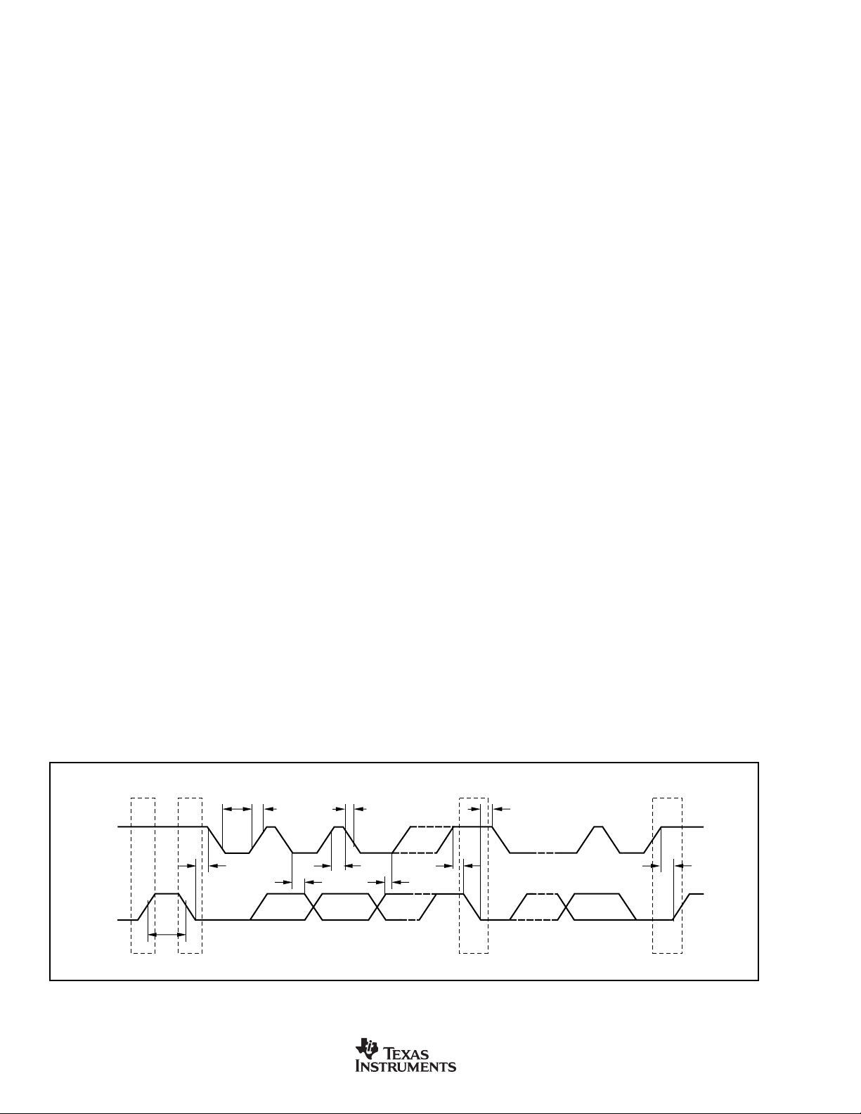
A timing diagram for an ADS1100 I
2
C transaction is shown in
Figure 1. Table III gives the parameters for this diagram.
ADS1100 I
The ADS1100 I
2
C ADDRESSES
2
C address is 1001aaa, where “aaa” are bits
set at the factory. The ADS1100 is available in eight different
verisons, each having a different I
2
C address. For example,
the ADS1100A0 has address 1001000, and the ADS1100A3
has address 1001011. See the Package/Ordering Information table for a complete listing.
2
The I
C address is the only difference between the eight
variants. In all other repsects, they operate identically.
Each variant of the ADS1100 is marked with “ADx,” where x
C
identifies the address variant. For example, the ADS1100A0 is
marked “AD0”, and the ADS1100A3 is marked “AD3”. See the
Package/Ordering Information table for a complete listing.
When the ADS1100 was first introduced, it was shipped with
only one address, 1001000, and was marked “BAAI.” That
device is identical to the currently shipping ADS1100A0
variant marked “AD0”.
SCL
SDA
t
(BUF)
PS S P
FIGURE 1. I2C Timing Diagram.
8
t
(LOW)
t
(HDSTA)
(HDDAT)
t
F
t
(HIGH)
t
(SUSTA)
t
(SUDAT)
t
(HDSTA)
t
(SUSTO)
t
R
t
ADS1100
www.ti.com
SBAS239B
Page 9

FAST MODE HIGH-SPEED MODE
PARAMETER MIN MAX MIN MAX UNITS
SCLK Operating Frequency f
Bus Free Time Between STOP and START Condition t
Hold Time After Repeated START Condition. t
After this period, the first clock is generated.
Repeated START Condition Setup Time t
STOP Condition Setup Time t
Data Hold Time t
Data Setup Time t
SCLK Clock LOW Period t
SCLK Clock HIGH Period t
Clock/Data Fall Time t
Clock/Data Rise Time t
(SCLK)
(BUF)
(HDSTA)
(SUSTA)
(SUSTO)
(HDDAT)
(SUDAT)
(LOW)
(HIGH)
600 160 ns
600 160 ns
600 160 ns
600 160 ns
00ns
100 10 ns
1300 160 ns
600 60 ns
F
R
0.4 3.4 MHz
300 160 ns
300 160 ns
TABLE III. Timing Diagram Definitions.
I2C GENERAL CALL
The ADS1100 responds to General Call Reset, which is an
address byte of 00H followed by a data byte of 06H. The
ADS1100 acknowledges both bytes.
On receiving a General Call Reset, the ADS1100 performs a
full internal reset, just as though it had been powered off and
then on. If a conversion is in process, it is interrupted; the
output register is set to zero, and the configuration register is
set to its default setting.
The ADS1100 always acknowledges the General Call address byte of 00
Call data bytes other than 04
, but it does not acknowledge any General
H
or 06H.
H
I2C DATA RATES
2
C bus operates in one of three speed modes: Stan-
The I
dard, which allows a clock frequency of up to 100kHz; Fast,
which allows a clock frequency of up to 400kHz; and Highspeed mode (also called Hs mode), which allows a clock
frequency of up to 3.4MHz. The ADS1100 is fully compatible
with all three modes.
No special action needs to be taken to use the ADS1100 in
Standard or Fast modes, but High-speed mode must be
activated. To activate High-speed mode, send a special
address byte of 00001XXX following the start condition,
where the XXX bits are unique to the Hs-capable master.
This byte is called the Hs master code. (Note that this is
different from normal address bytes: the low bit does not
indicate read/write status.) The ADS1100 will not acknowledge this byte; the I
2
C specification prohibits acknowledgment of the Hs master code. On receiving a master code, the
ADS1100 will switch on its High-speed mode filters, and will
communicate at up to 3.4MHz. The ADS1100 switches out of
Hs mode with the next stop condition.
For more information on High-speed mode, consult the I
2
specification.
REGISTERS
The ADS1100 has two registers that are accessible via its I
port. The output register contains the result of the last conversion; the configuration register allows you to change the
ADS1100’s operating mode and query the status of the device.
OUTPUT REGISTER
The 16-bit output register contains the result of the last
conversion in binary two’s complement format. Following
reset or power-up, the output register is cleared to zero; it
remains zero until the first conversion is completed. Therefore, if you read the ADS1100 just after reset or power-up,
you will read zero from the output register.
The output register’s format is shown in Table IV.
CONFIGURATION REGISTER
You can use the 8-bit configuration register to control the
ADS1100’s operating mode, data rate, and PGA settings.
The configuration register’s format is shown in Table V. The
default setting is 8CH.
BIT 7 654321 0
NAME ST/BSY 0 0 SC DR1 DR0 PGA1 PGA0
TABLE V. Configuration Register.
Bit 7: ST/BSY
The meaning of the ST/BSY bit depends on whether it is
being written to or read from.
In single conversion mode, writing a 1 to the ST/BSY bit
causes a conversion to start, and writing a 0 has no effect.
In continuous conversion mode, the ADS1100 ignores the
value written to ST/BSY.
C
2
C
BIT 1514131211109876543210
NAME D15 D14 D13 D12 D11 D10 D9 D8 D7 D6 D5 D4 D3 D2 D1 D0
TABLE IV. Output Register.
ADS1100
SBAS239B
www.ti.com
9
Page 10

When read in single conversion mode, ST/BSY indicates whether
the A/D converter is busy taking a conversion. If ST/BSY is read
as 1, the A/D converter is busy, and a conversion is taking
place; if 0, no conversion is taking place, and the result of the
last conversion is available in the output register.
In continuous mode, ST/BSY is always read as 1.
Bits 6-5: Reserved
Bits 6 and 5 must be set to zero.
Bit 4: SC
SC controls whether the ADS1100 is in continuous conversion or single conversion mode. When SC is 1, the ADS1100
is in single conversion mode; when SC is 0, the ADS1100 is
in continuous conversion mode. The default setting is 0.
Bits 3-2: DR
Bits 3 and 2 control the ADS1100’s data rate, as shown in
Table VI.
DR1 DR0 DATA RATE
0 0 128SPS
0 1 32SPS
1 0 16SPS
(1)
1
NOTE: (1) Default Setting.
(1)
1
8SPS
(1)
TABLE VI. DR Bits.
READING FROM THE ADS1100
You can read the output register and the contents of the
configuration register from the ADS1100. To do this, address
the ADS1100 for reading, and read three bytes from the
device. The first two bytes are the output register’s contents;
the third byte is the configuration register’s contents.
You do not always have to read three bytes from the
ADS1100. If you want only the contents of the output register, read only two bytes.
Reading more than three bytes from the ADS1100 has no
effect. All of the bytes beginning with the fourth will be FF
See Figure 2 for a timing diagram of an ADS1100 read
operation.
WRITING TO THE ADS1100
You can write new contents into the configuration register
(you cannot change the contents of the output register). To
do this, address the ADS1100 for writing, and write one byte
to it. This byte is written into the configuration register.
Writing more than one byte to the ADS1100 has no effect.
The ADS1100 will ignore any bytes sent to it after the first
one, and it will only acknowledge the first byte.
See Figure 3 for a timing diagram of an ADS1100 write
operation.
.
H
Bits 1-0: PGA
Bits 1 and 0 control the ADS1100’s gain setting, as shown in
Table VII.
PGA1 PGA0 GAIN
(1)
0
01 2
10 4
NOTE: (1) Default Setting.
11 8
(1)
0
(1)
1
TABLE VII. PGA Bits.
10
www.ti.com
ADS1100
SBAS239B
Page 11
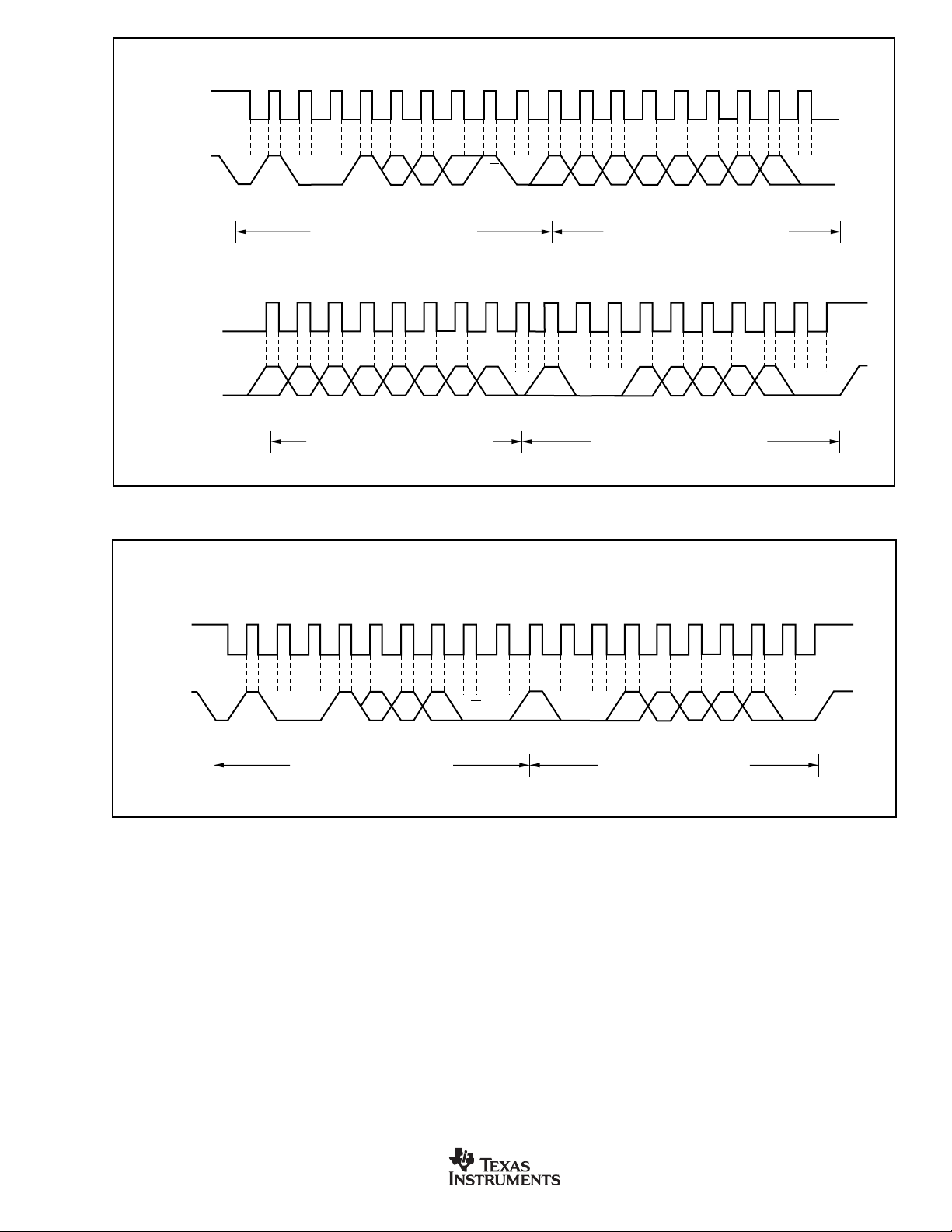
SCL
191
9
…
SDA
SCL
(Continued)
SDA
(Continued)
Start By
Master
…
…
1 0 0 1 A2 A1 A0 R/W
Frame 1: I2C Slave Address Byte Frame 2: Output Register Upper Byte
1
D7 D6 D5 D4 D3 D2 D1 D0
From
ADS1100
Frame 3: Output Register Lower Byte Frame 4: Configuration Register
FIGURE 2. Timing Diagram for Reading From the ADS1100.
D15 D14 D13 D12 D11 D10 D9 D8
ACK By
ADS1100
91
ACK By
Master
ST/
0 0 SC DR1 DR0
BSY
From
ADS1100
From
ADS1100
(Optional)
PGA1 PGA0
9
ACK By
Master
…
ACK By
Master
Stop By
Master
1919
SCL
SDA
Start By
Master
001A2A1 A0 R/W
1
Frame 1: I2C Slave Address Byte Frame 2: Configuration Register
FIGURE 3. Timing Diagram for Writing to the ADS1100.
ACK By
ADS1100
ST/
0 0 SC DR1 DR0
BSY
PGA1 PGA0
ACK By
ADS1100
Stop By
Master
ADS1100
SBAS239B
www.ti.com
11
Page 12
APPLICATIONS INFORMATION
The sections that follow give example circuits and tips for
using the ADS1100 in various situations.
An evaluation board, the ADS1100EVM, is available. This
small, simple board connects to an RS-232 serial port on
almost any PC. The supplied software simulates a digital
voltmeter, and also displays raw output codes in hex and
decimal. All features of the ADS1100 can be controlled from
the main window. For more information, contact TI or your
local TI representative, or visit the Texas Instruments website
at http://www.ti.com/.
BASIC CONNECTIONS
For many applications, connecting the ADS1100 is extremely
simple. A basic connection diagram for the ADS1100 is
shown in Figure 4.
The fully differential voltage input of the ADS1100 is ideal for
connection to differential sources with moderately low source
impedance, such as bridge sensors and thermistors. Although the ADS1100 can read bipolar differential signals, it
cannot accept negative voltages on either input. It may be
helpful to think of the ADS1100 positive voltage input as noninverting, and of the negative input as inverting.
When the ADS1100 is converting, it draws current in short
spikes. The 0.1µF bypass capacitor supplies the momentary
bursts of extra current needed from the supply.
The ADS1100 interfaces directly to standard mode, fast
mode, and high-speed mode I
microcontroller’s I
2
C peripheral, including master-only and
2
C controllers. Any
2
non-multiiple-master I
C peripherals, will work with the
ADS1100. The ADS1100 does not perform clock-stretching
(i.e., it never pulls the clock line low), so it is not necessary
to provide for this unless other devices are on the same I
2
bus.
Pull-up resistors are necessary on both the SDA and SCL
lines because I
2
C bus drivers are open-drain. The size of
these resistors depends on the bus operating speed and
capacitance of the bus lines. Higher-value resistors consume
less power, but increase the transition times on the bus,
limiting the bus speed. Lower-value resistors allow higher
speed at the expense of higher power consumption. Long
bus lines have higher capacitance and require smaller pullup resistors to compensate. The resistors should not be too
small; if they are, the bus drivers may not be able to pull the
bus lines low.
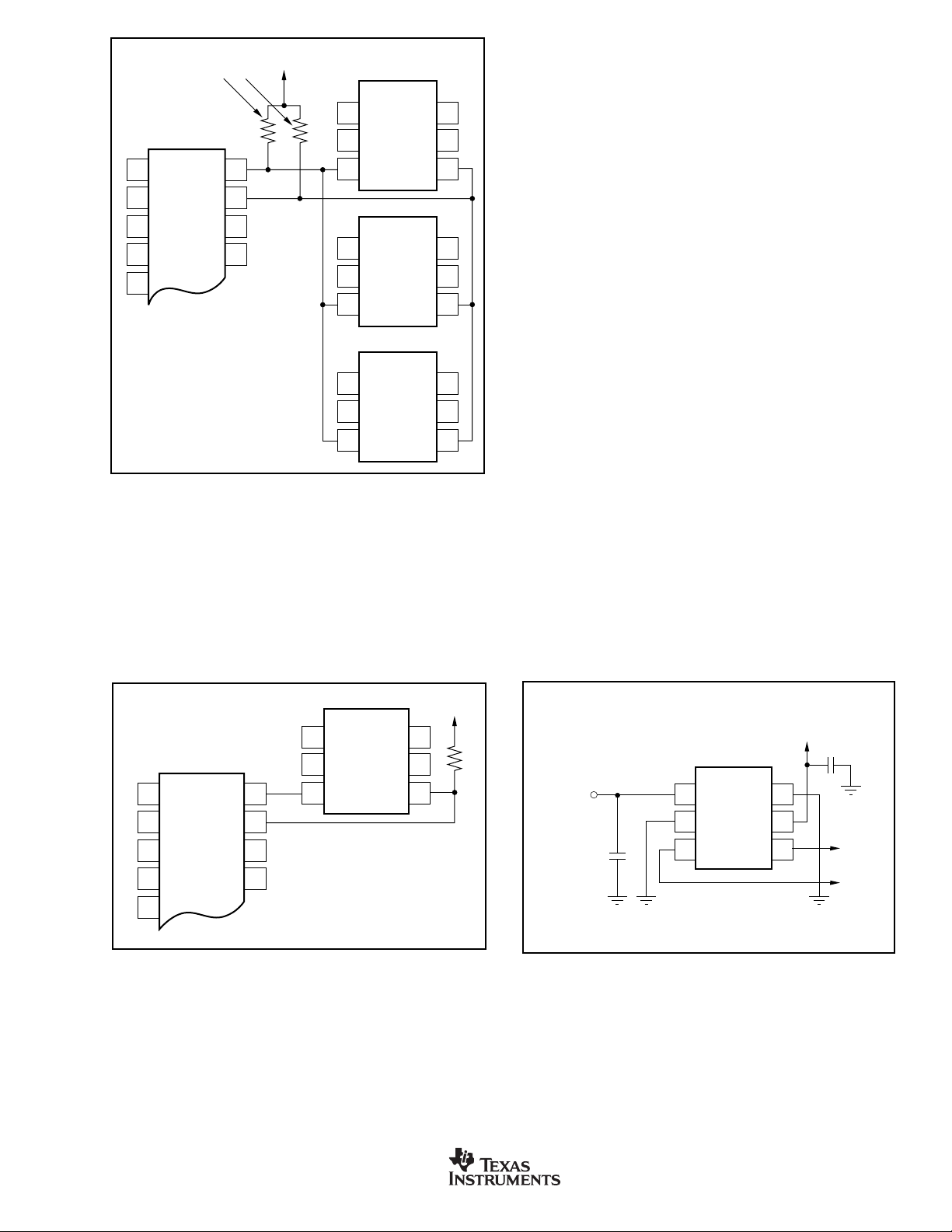
CONNECTING MULTIPLE DEVICES
Connecting multiple ADS1100s to a single bus is almost
trivial. The ADS1100 is available in eight different versions, each of which has a different I
example showing three ADS1100s connected on a single
bus is shown in Figure 5. Up to eight ADS1100s (provided
their addresses are different) can be connected to a single
bus.
Note that only one set of pull-up resistors is needed per bus.
You might find that you need to lower the pull-up resistor
values slightly to compensate for the additional bus capacitance presented by multiple devices and increased line
length.
2
C address. An
C
2
I
C Pull-Up Resistors
1kΩ to 10kΩ (typ.)
Microcontroller or
Microprocessor
2
with I
C Port
SCL
SDA
FIGURE 4. Typical Connections of the ADS1100.
V
DD
Positive Input
(0V to 5V)
1
2
3
ADS1100
V
IN+
GND
SCL
V
IN–
V
SDA
DD
Negative Input
(0V to 5V)
V
DD
6
5
4
4.7µF (typ.)
12
www.ti.com
ADS1100
SBAS239B
Page 13
2
C Pull-Up Resistors
I
1kΩ to 10kΩ (typ.)
Microcontroller or
Microprocessor
2
with I
C Port
SCL
SDA
NOTE: ADS1100 power
and input connections
omitted for clarity.
V
DD
ADS1100A0
V
V
1
IN+
GND
2
SCL
3
ADS1100A1
V
1
IN+
GND
2
SCL
3
ADS1100A2
V
1
IN+
GND
2
SCL
3
IN–
V
SDA
V
IN–
V
SDA
V
IN–
V
SDA
6
5
DD
4
6
5
DD
4
6
5
DD
4
FIGURE 5. Connecting Multiple ADS1100s.
USING GPIO PORTS FOR I2C
Most microcontrollers have programmable input/output pins
that can be set in software to act as inputs or outputs. If an
2
I
C controller is not available, the ADS1100 can be connected to GPIO pins, and the I
bit-banged, in software. An example of this for a single
ADS1100 is shown in Figure 6.
2
C bus protocol simulated, or
Note that no pull-up resistor is shown on the SCL line. In this
simple case, the resistor is not needed; the microcontroller
can simply leave the line on output, and set it to one or zero
as appropriate. It can do this because the ADS1100 never
drives its clock line low. This technique can also be used with
multiple devices, and has the advantage of lower current
consumption due to the absence of a resistive pull-up.
If there are any devices on the bus that may drive their clock
lines low, the above method should not be used; the SCL line
should be high-Z or zero and a pull-up resistor provided as
usual. Note also that this cannot be done on the SDA line in
any case, because the ADS1100 does drive the SDA line low
from time to time, as all I
2
C devices do.
Some microcontrollers have selectable strong pull-up circuits
built in to their GPIO ports. In some cases, these can be
switched on and used in place of an external pull-up resistor.
Weak pull-ups are also provided on some microcontrollers,
but usually these are too weak for I
2
C communication. If
there is any doubt about the matter, test the circuit before
committing it to production.
SINGLE-ENDED INPUTS
Although the ADS1100 has a fully differential input, it can
easily measure single-ended signals. A simple single-ended
connection scheme is shown in Figure 7. The ADS1100 is
configured for single-ended measurement by grounding either of its input pins, usually V
signal to V
to V
DD
+. The single-ended signal can range from –0.2V
IN
+ 0.3V. The ADS1100 loses no linearity anywhere in
its input range. Negative voltages cannot be applied to this
circuit because the ADS1100 inputs can only accept positive
voltages.
–, and applying the input
IN
V
DD
6
5
4
Microcontroller or
Microprocessor
2
with I
C Port
SCL
SDA
ADS1100
V
1
GND
2
SCL
3
NOTE: ADS1100 power
and input connections
omitted for clarity.
V
IN+
V
SDA
IN–
DD
FIGURE 6. Using GPIO with a Single ADS1100.
Bit-banging I2C with GPIO pins can be done by setting the
GPIO line to zero and toggling it between input and output
modes to apply the proper bus states. To drive the line low,
the pin is set to output a zero; to let the line go high, the pin
is set to input. When the pin is set to input, the state of the
pin can be read; if another device is pulling the line low, this
will read as a zero in the port’s input register.
V
DD
0V - V
Single-Ended
Filter Capacitor
33pF to 100pF
DD
(typ.)
1
2
3
ADS1100
V
IN+
GND
SCL
V
V
SDA
6
IN–
5
DD
4
Output
Codes
0-32767
FIGURE 7. Measuring Single-Ended Inputs.
The ADS1100 input range is bipolar differential with respect
to the reference, i.e. ±V
. The single-ended circuit shown in
DD
Figure 7 covers only half the ADS1100 input scale because
it does not produce differentially negative inputs; therefore,
one bit of resolution is lost. The Burr-Brown DRV134 balanced line driver from Texas Instruments can be employed
to regain this bit for single-ended signals.
ADS1100
SBAS239B
www.ti.com
13
Page 14

Negative input voltages must be level-shifted. A good candidate for this function is the Texas Instruments THS4130
differential amplifier, which can output fully differential signals. This device can also help recover the lost bit noted
previously for single-ended positive signals. Level shifting
can also be performed using the DRV134.
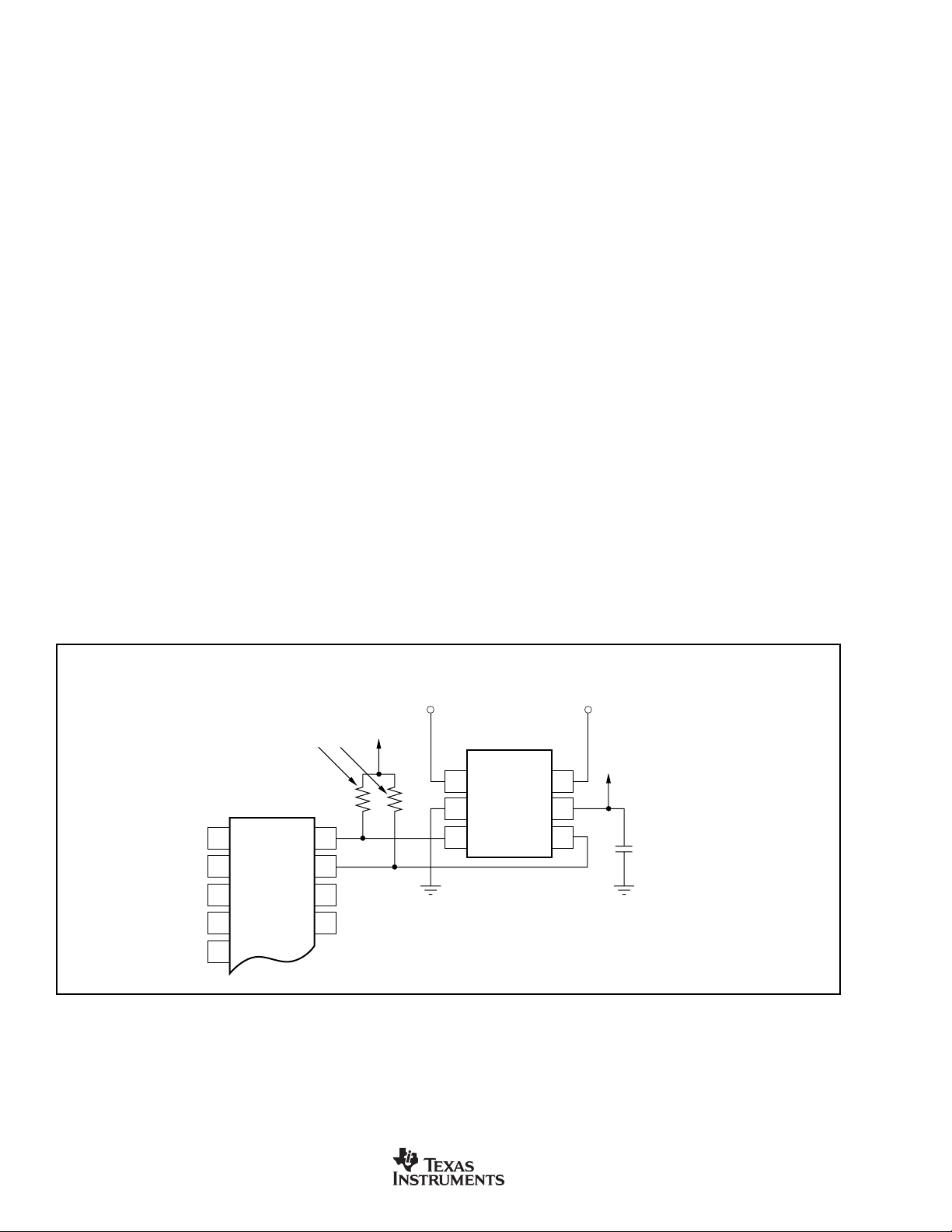
WHEATSTONE BRIDGE SENSOR
The ADS1100 has a fully differential high-impedance input
stage and internal gain circuitry, which makes it a good
candidate for bridge-sensor measurement. An example is
shown in Figure 9.
LOW-SIDE CURRENT MONITOR
Figure 8 shows a circuit for a low-side shunt-type current
monitor. The circuit reads the voltage across a shunt resistor,
which is sized as small as possible while still giving a readable
output voltage. This voltage is amplified by an OPA335 lowdrift op-amp, and the result is read by the ADS1100.
11.5kΩ
1kΩ R
5V
OPA335
G = 12.5
FS = 0.63V
R
49.9kΩ
–5V
(1)
3
V
Load
(2)
S
NOTE: (1) Pull-down resistor to allow accurate swing to 0V.
(2) R
is sized for a 50mV drop at full-scale current.
S
5V
ADS1100
2
C
I
(PGA Gain = 8)
5V FS
V
ADS1100
V
IN+
GND
SCL
I
2
C I/O
DD
E+
E–
V
6
IN–
V
5
DD
SDA
4
Bridge
Sensor
V– V+
1
2
3
V
DD
4.7µF
FIGURE 8. Low-Side Current Measurement.
It is suggested that the ADS1100 be operated at a gain of 8. The
gain of the OPA335 can then be set lower. For a gain of 8, the
op amp should be set up to give a maximum output voltage of
no greater than 0.75V. If the shunt resistor is sized to provide
a maximum voltage drop of 50mV at full-scale current, the
full-scale input to the ADS1100 is 0.63V.
FIGURE 9. Measuring a Wheatstone Bridge Sensor.
The Wheatstone bridge sensor is connected directly to the
ADS1100 without intervening instrumentation amplifiers; a
single, small input capacitor provides rejection of high-frequency interference. The excitation voltage of the bridge is
the power supply, which is also the ADS1100 reference
voltage. The measurement is, therefore, ratiometric. In this
circuit, the ADS1100 would typically be operated at a gain of
8. The input range in this case is ±0.75 volts.
14
www.ti.com
ADS1100
SBAS239B
Page 15

Many resistive bridge sensors, such as strain gauges, have
very small full-scale output ranges. For these sensors, the
measurement resolution obtainable without additional amplification can be low. For example, if the bridge sensor output
is ±20mV, the ADS1100 outputs codes from approximately
–873 to +873, resulting in a best-case resolution of around 11
bits. If higher resolution is required, it is best to supply an
external instrumentation amplifier to bring the signal to full
scale.
ADVICE
The ADS1100 is fabricated in a small-geometry low-voltage
process. The analog inputs feature protection diodes to the
supply rails. However, the current-handling ability of these
diodes is limited, and the ADS1100 can be permanently
damaged by analog input voltages that remain more than
approximately 300mV beyond the rails for extended periods.
One way to protect against overvoltage is to place currentlimiting resistors on the input lines. The ADS1100 analog
inputs can withstand momentary currents of as large as
10mA.
The previous paragraph does not apply to the I
which can both be driven to 6V regardless of the supply.
2
C ports,
If the ADS1100 is driven by an op amp with high voltage
supplies, such as ±12V, protection should be provided, even
if the op amp is configured so that it will not output out-ofrange voltages. Many op amps seek to one of the supply rails
immediately when power is applied, usually before the input
has stabilized; this momentary spike can damage the ADS1100.
Sometimes this damage is incremental and results in slow,
long-term failure—which can be distastrous for permanently
installed, low-maintenance systems.
If you use an op amp or other front-end circuitry with the
ADS1100, be sure to take the performance characteristics of this
circuitry into account. A chain is only as strong as its weakest link.
LAYOUT TIPS
PCB layout for the ADS1100 is relatively undemanding.
16-bit performance is not difficult to achieve.
Any data converter is only as good as its reference. For the
ADS1100, the reference is the power supply, and the power
supply must be clean enough to achieve the desired performance. If a power-supply filter capacitor is used, it should be
placed close to the V
capacitor and the pin. The trace leading to the pin should be as
wide as possible, even if it must be necked down at the device.
pin, with no vias placed between the
DD
ADS1100
SBAS239B
www.ti.com
15
Page 16

PACKAGE OPTION ADDENDUM
www.ti.com 7-Sep-2009
PACKAGING INFORMATION
Orderable Device Status
ADS1100A0IDBVR ACTIVE SOT-23 DBV 6 3000 Green (RoHS &
ADS1100A0IDBVRG4 ACTIVE SOT-23 DBV 6 3000 Green (RoHS &
ADS1100A0IDBVT ACTIVE SOT-23 DBV 6 250 Green (RoHS &
ADS1100A0IDBVTG4 ACTIVE SOT-23 DBV 6 250 Green (RoHS &
ADS1100A1IDBVR ACTIVE SOT-23 DBV 6 3000 Green (RoHS &
ADS1100A1IDBVRG4 ACTIVE SOT-23 DBV 6 3000 Green (RoHS &
ADS1100A1IDBVT ACTIVE SOT-23 DBV 6 250 Green (RoHS &
ADS1100A1IDBVTG4 ACTIVE SOT-23 DBV 6 250 Green (RoHS &
ADS1100A2IDBVR ACTIVE SOT-23 DBV 6 3000 Green (RoHS &
ADS1100A2IDBVRG4 ACTIVE SOT-23 DBV 6 3000 Green (RoHS &
ADS1100A2IDBVT ACTIVE SOT-23 DBV 6 250 Green (RoHS &
ADS1100A2IDBVTG4 ACTIVE SOT-23 DBV 6 250 Green (RoHS &
ADS1100A3IDBVR ACTIVE SOT-23 DBV 6 3000 Green (RoHS &
ADS1100A3IDBVRG4 ACTIVE SOT-23 DBV 6 3000 Green (RoHS &
ADS1100A3IDBVT ACTIVE SOT-23 DBV 6 250 Green (RoHS &
ADS1100A3IDBVTG4 ACTIVE SOT-23 DBV 6 250 Green (RoHS &
ADS1100A4IDBVR ACTIVE SOT-23 DBV 6 3000 Green (RoHS &
ADS1100A4IDBVRG4 ACTIVE SOT-23 DBV 6 3000 Green (RoHS &
ADS1100A4IDBVT ACTIVE SOT-23 DBV 6 250 Green (RoHS &
ADS1100A4IDBVTG4 ACTIVE SOT-23 DBV 6 250 Green (RoHS &
ADS1100A5IDBVR ACTIVE SOT-23 DBV 6 3000 Green (RoHS &
ADS1100A5IDBVRG4 ACTIVE SOT-23 DBV 6 3000 Green (RoHS &
ADS1100A5IDBVT ACTIVE SOT-23 DBV 6 250 Green (RoHS &
ADS1100A5IDBVTG4 ACTIVE SOT-23 DBV 6 250 Green (RoHS &
ADS1100A6IDBVR ACTIVE SOT-23 DBV 6 3000 Green (RoHS &
(1)
Package
Type
Package
Drawing
Pins Package
Qty
Eco Plan
no Sb/Br)
no Sb/Br)
no Sb/Br)
no Sb/Br)
no Sb/Br)
no Sb/Br)
no Sb/Br)
no Sb/Br)
no Sb/Br)
no Sb/Br)
no Sb/Br)
no Sb/Br)
no Sb/Br)
no Sb/Br)
no Sb/Br)
no Sb/Br)
no Sb/Br)
no Sb/Br)
no Sb/Br)
no Sb/Br)
no Sb/Br)
no Sb/Br)
no Sb/Br)
no Sb/Br)
no Sb/Br)
(2)
Lead/Ball Finish MSL Peak Temp
CU NIPDAU Level-1-260C-UNLIM
CU NIPDAU Level-1-260C-UNLIM
CU NIPDAU Level-1-260C-UNLIM
CU NIPDAU Level-1-260C-UNLIM
Call TI Level-1-260C-UNLIM
Call TI Level-1-260C-UNLIM
CU NIPDAU Level-1-260C-UNLIM
CU NIPDAU Level-1-260C-UNLIM
CU NIPDAU Level-1-260C-UNLIM
CU NIPDAU Level-1-260C-UNLIM
CU NIPDAU Level-1-260C-UNLIM
CU NIPDAU Level-1-260C-UNLIM
CU NIPDAU Level-1-260C-UNLIM
CU NIPDAU Level-1-260C-UNLIM
CU NIPDAU Level-1-260C-UNLIM
CU NIPDAU Level-1-260C-UNLIM
CU NIPDAU Level-1-260C-UNLIM
CU NIPDAU Level-1-260C-UNLIM
CU NIPDAU Level-1-260C-UNLIM
CU NIPDAU Level-1-260C-UNLIM
CU NIPDAU Level-1-260C-UNLIM
CU NIPDAU Level-1-260C-UNLIM
CU NIPDAU Level-1-260C-UNLIM
CU NIPDAU Level-1-260C-UNLIM
CU NIPDAU Level-1-260C-UNLIM
(3)
Addendum-Page 1
Page 17

PACKAGE OPTION ADDENDUM
www.ti.com 7-Sep-2009
Orderable Device Status
(1)
Package
Type
Package
Drawing
Pins Package
Qty
Eco Plan
ADS1100A6IDBVRG4 ACTIVE SOT-23 DBV 6 3000 Green (RoHS &
(2)
Lead/Ball Finish MSL Peak Temp
CU NIPDAU Level-1-260C-UNLIM
(3)
no Sb/Br)
ADS1100A6IDBVT ACTIVE SOT-23 DBV 6 250 Green (RoHS &
CU NIPDAU Level-1-260C-UNLIM
no Sb/Br)
ADS1100A6IDBVTG4 ACTIVE SOT-23 DBV 6 250 Green (RoHS &
CU NIPDAU Level-1-260C-UNLIM
no Sb/Br)
ADS1100A7IDBVR ACTIVE SOT-23 DBV 6 3000 Green (RoHS &
CU NIPDAU Level-1-260C-UNLIM
no Sb/Br)
ADS1100A7IDBVRG4 ACTIVE SOT-23 DBV 6 3000 Green (RoHS &
CU NIPDAU Level-1-260C-UNLIM
no Sb/Br)
ADS1100A7IDBVT ACTIVE SOT-23 DBV 6 250 Green (RoHS &
CU NIPDAU Level-1-260C-UNLIM
no Sb/Br)
ADS1100A7IDBVTG4 ACTIVE SOT-23 DBV 6 250 Green (RoHS &
CU NIPDAU Level-1-260C-UNLIM
no Sb/Br)
(1)
The marketing status values are defined as follows:
ACTIVE: Product device recommended for new designs.
LIFEBUY: TI has announced that the device will be discontinued, and a lifetime-buy period is in effect.
NRND: Not recommended for new designs. Device is in production to support existing customers, but TI does not recommend using this part in
a new design.
PREVIEW: Device has been announced but is not in production. Samples may or may not be available.
OBSOLETE: TI has discontinued the production of the device.
(2)
Eco Plan - The planned eco-friendly classification: Pb-Free (RoHS), Pb-Free (RoHS Exempt), or Green (RoHS & no Sb/Br) - please check
http://www.ti.com/productcontent for the latest availability information and additional product content details.
TBD: The Pb-Free/Green conversion plan has not been defined.
Pb-Free (RoHS): TI's terms "Lead-Free" or "Pb-Free" mean semiconductor products that are compatible with the current RoHS requirements
for all 6 substances, including the requirement that lead not exceed 0.1% by weight in homogeneous materials. Where designed to be soldered
at high temperatures, TI Pb-Free products are suitable for use in specified lead-free processes.
Pb-Free (RoHS Exempt): This component has a RoHS exemption for either 1) lead-based flip-chip solder bumps used between the die and
package, or 2) lead-based die adhesive used between the die and leadframe. The component is otherwise considered Pb-Free (RoHS
compatible) as defined above.
Green (RoHS & no Sb/Br): TI defines "Green" to mean Pb-Free (RoHS compatible), and free of Bromine (Br) and Antimony (Sb) based flame
retardants (Br or Sb do not exceed 0.1% by weight in homogeneous material)
(3)
MSL, Peak Temp. -- The Moisture Sensitivity Level rating according to the JEDEC industry standard classifications, and peak solder
temperature.
Important Information and Disclaimer:The information provided on this page represents TI's knowledge and belief as of the date that it is
provided. TI bases its knowledge and belief on information provided by third parties, and makes no representation or warranty as to the
accuracy of such information. Efforts are underway to better integrate information from third parties. TI has taken and continues to take
reasonable steps to provide representative and accurate information but may not have conducted destructive testing or chemical analysis on
incoming materials and chemicals. TI and TI suppliers consider certain information to be proprietary, and thus CAS numbers and other limited
information may not be available for release.
In no event shall TI's liability arising out of such information exceed the total purchase price of the TI part(s) at issue in this document sold by TI
to Customer on an annual basis.
Addendum-Page 2
Page 18

PACKAGE MATERIALS INFORMATION
www.ti.com
TAPE AND REEL INFORMATION
20-Dec-2008
*All dimensions are nominal
Device Package
Type
ADS1100A0IDBVR SOT-23 DBV 6 3000 180.0 8.4 3.2 3.1 1.39 4.0 8.0 Q3
ADS1100A0IDBVT SOT-23 DBV 6 250 180.0 8.4 3.2 3.1 1.39 4.0 8.0 Q3
ADS1100A1IDBVR SOT-23 DBV 6 3000 180.0 8.4 3.2 3.1 1.39 4.0 8.0 Q3
ADS1100A1IDBVT SOT-23 DBV 6 250 180.0 8.4 3.2 3.1 1.39 4.0 8.0 Q3
ADS1100A2IDBVR SOT-23 DBV 6 3000 180.0 8.4 3.2 3.1 1.39 4.0 8.0 Q3
ADS1100A2IDBVT SOT-23 DBV 6 250 180.0 8.4 3.2 3.1 1.39 4.0 8.0 Q3
ADS1100A3IDBVR SOT-23 DBV 6 3000 180.0 8.4 3.2 3.1 1.39 4.0 8.0 Q3
ADS1100A3IDBVT SOT-23 DBV 6 250 180.0 8.4 3.2 3.1 1.39 4.0 8.0 Q3
ADS1100A4IDBVR SOT-23 DBV 6 3000 180.0 8.4 3.2 3.1 1.39 4.0 8.0 Q3
ADS1100A4IDBVT SOT-23 DBV 6 250 180.0 8.4 3.2 3.1 1.39 4.0 8.0 Q3
ADS1100A5IDBVR SOT-23 DBV 6 3000 180.0 8.4 3.2 3.1 1.39 4.0 8.0 Q3
ADS1100A5IDBVT SOT-23 DBV 6 250 180.0 8.4 3.2 3.1 1.39 4.0 8.0 Q3
ADS1100A6IDBVR SOT-23 DBV 6 3000 180.0 8.4 3.2 3.1 1.39 4.0 8.0 Q3
ADS1100A6IDBVT SOT-23 DBV 6 250 180.0 8.4 3.2 3.1 1.39 4.0 8.0 Q3
ADS1100A7IDBVR SOT-23 DBV 6 3000 180.0 8.4 3.2 3.1 1.39 4.0 8.0 Q3
ADS1100A7IDBVT SOT-23 DBV 6 250 180.0 8.4 3.2 3.1 1.39 4.0 8.0 Q3
Package
Drawing
Pins SPQ Reel
Diameter
(mm)
Reel
Width
W1 (mm)
A0 (mm) B0 (mm) K0 (mm) P1
(mm)W(mm)
Pin1
Quadrant
Pack Materials-Page 1
Page 19

PACKAGE MATERIALS INFORMATION
www.ti.com
20-Dec-2008
*All dimensions are nominal
Device Package Type Package Drawing Pins SPQ Length (mm) Width (mm) Height (mm)
ADS1100A0IDBVR SOT-23 DBV 6 3000 190.5 212.7 31.8
ADS1100A0IDBVT SOT-23 DBV 6 250 190.5 212.7 31.8
ADS1100A1IDBVR SOT-23 DBV 6 3000 190.5 212.7 31.8
ADS1100A1IDBVT SOT-23 DBV 6 250 190.5 212.7 31.8
ADS1100A2IDBVR SOT-23 DBV 6 3000 190.5 212.7 31.8
ADS1100A2IDBVT SOT-23 DBV 6 250 190.5 212.7 31.8
ADS1100A3IDBVR SOT-23 DBV 6 3000 190.5 212.7 31.8
ADS1100A3IDBVT SOT-23 DBV 6 250 190.5 212.7 31.8
ADS1100A4IDBVR SOT-23 DBV 6 3000 190.5 212.7 31.8
ADS1100A4IDBVT SOT-23 DBV 6 250 190.5 212.7 31.8
ADS1100A5IDBVR SOT-23 DBV 6 3000 190.5 212.7 31.8
ADS1100A5IDBVT SOT-23 DBV 6 250 190.5 212.7 31.8
ADS1100A6IDBVR SOT-23 DBV 6 3000 190.5 212.7 31.8
ADS1100A6IDBVT SOT-23 DBV 6 250 190.5 212.7 31.8
ADS1100A7IDBVR SOT-23 DBV 6 3000 190.5 212.7 31.8
ADS1100A7IDBVT SOT-23 DBV 6 250 190.5 212.7 31.8
Pack Materials-Page 2
Page 20

Page 21

IMPORTANT NOTICE
Texas Instruments Incorporated and its subsidiaries (TI) reserve the right to make corrections, modifications, enhancements, improvements,
and other changes to its products and services at any time and to discontinue any product or service without notice. Customers should
obtain the latest relevant information before placing orders and should verify that such information is current and complete. All products are
sold subject to TI’s terms and conditions of sale supplied at the time of order acknowledgment.
TI warrants performance of its hardware products to the specifications applicable at the time of sale in accordance with TI’s standard
warranty. Testing and other quality control techniques are used to the extent TI deems necessary to support this warranty. Except where
mandated by government requirements, testing of all parameters of each product is not necessarily performed.
TI assumes no liability for applications assistance or customer product design. Customers are responsible for their products and
applications using TI components. To minimize the risks associated with customer products and applications, customers should provide
adequate design and operating safeguards.
TI does not warrant or represent that any license, either express or implied, is granted under any TI patent right, copyright, mask work right,
or other TI intellectual property right relating to any combination, machine, or process in which TI products or services are used. Information
published by TI regarding third-party products or services does not constitute a license from TI to use such products or services or a
warranty or endorsement thereof. Use of such information may require a license from a third party under the patents or other intellectual
property of the third party, or a license from TI under the patents or other intellectual property of TI.
Reproduction of TI information in TI data books or data sheets is permissible only if reproduction is without alteration and is accompanied
by all associated warranties, conditions, limitations, and notices. Reproduction of this information with alteration is an unfair and deceptive
business practice. TI is not responsible or liable for such altered documentation. Information of third parties may be subject to additional
restrictions.
Resale of TI products or services with statements different from or beyond the parameters stated by TI for that product or service voids all
express and any implied warranties for the associated TI product or service and is an unfair and deceptive business practice. TI is not
responsible or liable for any such statements.
TI products are not authorized for use in safety-critical applications (such as life support) where a failure of the TI product would reasonably
be expected to cause severe personal injury or death, unless officers of the parties have executed an agreement specifically governing
such use. Buyers represent that they have all necessary expertise in the safety and regulatory ramifications of their applications, and
acknowledge and agree that they are solely responsible for all legal, regulatory and safety-related requirements concerning their products
and any use of TI products in such safety-critical applications, notwithstanding any applications-related information or support that may be
provided by TI. Further, Buyers must fully indemnify TI and its representatives against any damages arising out of the use of TI products in
such safety-critical applications.
TI products are neither designed nor intended for use in military/aerospace applications or environments unless the TI products are
specifically designated by TI as military-grade or "enhanced plastic." Only products designated by TI as military-grade meet military
specifications. Buyers acknowledge and agree that any such use of TI products which TI has not designated as military-grade is solely at
the Buyer's risk, and that they are solely responsible for compliance with all legal and regulatory requirements in connection with such use.
TI products are neither designed nor intended for use in automotive applications or environments unless the specific TI products are
designated by TI as compliant with ISO/TS 16949 requirements. Buyers acknowledge and agree that, if they use any non-designated
products in automotive applications, TI will not be responsible for any failure to meet such requirements.
Following are URLs where you can obtain information on other Texas Instruments products and application solutions:
Products Applications
Amplifiers amplifier.ti.com Audio www.ti.com/audio
Data Converters dataconverter.ti.com Automotive www.ti.com/automotive
DLP® Products www.dlp.com Broadband www.ti.com/broadband
DSP dsp.ti.com Digital Control www.ti.com/digitalcontrol
Clocks and Timers www.ti.com/clocks Medical www.ti.com/medical
Interface interface.ti.com Military www.ti.com/military
Logic logic.ti.com Optical Networking www.ti.com/opticalnetwork
Power Mgmt power.ti.com Security www.ti.com/security
Microcontrollers microcontroller.ti.com Telephony www.ti.com/telephony
RFID www.ti-rfid.com Video & Imaging www.ti.com/video
RF/IF and ZigBee® Solutions www.ti.com/lprf Wireless www.ti.com/wireless
Mailing Address: Texas Instruments, Post Office Box 655303, Dallas, Texas 75265
Copyright © 2009, Texas Instruments Incorporated
 Loading...