

Texas Instruments ADC1 D (RF )RB Series, ADC12D800RF, ADC12D1600RF, ADC12D1800RF, ADC12D1600 User Manual
...Page 1

ADC1xDxxxx(RF)RB Reference Board
User's Guide
Literature Number: SNAU146
September 2013
Page 2
ADC1xDxxxx(RF)RB Reference Board
1 Overview
The ADC1xDxxxx(RF)RB demonstrates a high-performance signal acquisition sub-system that achieves
10/12-bit resolution and corresponding SNR and dynamic range on two channels at signal frequencies in
excess of 1.0 GHz and sampling rates of up to 1.8 GS/s on two channels or one channel at a sampling
rate of up to 3.6 GHz.
Since the 10- and 12-bit GSPS ADC family is pin-compatible, the same PCB is able to support the
following devices:
• ADC12D1800RF, ADC12D1600RF, ADC12D800RF
• ADC12D1800, ADC12D1600
• ADC10D1500
In some cases, the same board may be used to evaluate two different products, with the addition of an
external signal generator. For example, to evaluate the ADC10D1000, use the ADC10D1500RB with an
external clock signal generator running at 1GHz. The table below shows which Reference Board (RB) to
use to evaluate which product.
User's Guide
SNAU146–September 2013
Figure 1. ADC1xDxxx_board1
2
ADC1xDxxxx(RF)RB Reference Board SNAU146–September 2013
Copyright © 2013, Texas Instruments Incorporated
Submit Documentation Feedback
Page 3
www.ti.com
The board showcases the following Texas Instruments devices:
• ADC1xDxxxx(RF) analog-to-digital converter
• LMX2541 clock synthesizer
• LP3878 and LP38513-ADJ linear LDO regulators
• LM20242, LM25576 and LM26400 switching regulators
• LM3880 power sequencing controller
• LM95233 temperature sensor
In addition, the board also employs the Xilinx XC4VLX25-11FFG668 Virtex-4 FPGA for the critical
function of capturing the high-speed digital data sourced by the ADC.
Overview
Table 1. Reference Board to Evaluate GSPS ADC
Product to Evaluate Reference Board to Use
ADC12D1800RF ADC12D1800RFRB
ADC12D1600RF ADC12D1600RFRB
ADC12D1000RF ADC12D1600RFRB
ADC12D800RF ADC12D800RFRB
ADC12D500RF ADC12D800RFRB
ADC12D1800 ADC12D1800RB
ADC12D1600 ADC12D1600RB
ADC12D1000 ADC12D1600RB
ADC10D1500 ADC10D1500RB
ADC10D1000 ADC10D1500RB
1.1 Features
❏ Demonstrates the ADC1xDxxxx(RF)'s typical dynamic performance – see the datasheet for full details.
❏ Dual channel sample rates of up to 1.8 GS/s (limited by the ADC specifications and the FPGA capture
limitations)
❏ Single channel (Interleaved) sample rates of up to 3.6 GS/s (limited by the ADC specifications and the
FPGA capture limitations)
❏ FMC Expansion Header for streaming data capture
❏ SMA I/O for easy AutoSync feature evaluation
❏ External Hardware Trigger
❏ Status LEDs
❏ On-board LMX2541 based clock circuit with option for a selectable external clock
❏ A complete high-performance low-noise power management section for the ADC, clock circuit, FPGA
and USB controller
❏ Single +12V power adapter input
❏ Simplicity and performance of USB 2.0 connection to the PC
❏ Functions with Texas Instruments' latest WaveVision 5 signal-path control and analysis software
SNAU146–September 2013 ADC1xDxxxx(RF)RB Reference Board
Submit Documentation Feedback
Copyright © 2013, Texas Instruments Incorporated
3
Page 4

Overview
1.2 Packing List
The ADC1xDxxxx(RF)RB kit consists of the following components:
• ADC1xDxxxx(RF)RB Reference Board
• Hardware Kit Including
– 110V-240V AC to +12V DC Power Adapter
– USB cable
– 4 – DC blocks
– 2 – 50Ω terminators
– 1 – ADC-LD-BB low distortion balun board useful bandwidth of 400 MHz to 3 GHz)
– 1 – ADC-WB-BB wide band balun board (useful bandwidth of 4.5 MHz to 3 GHz)
– 4 – 6” SMA cables
The most up-to-date documentation can be found on the product web folder; the Design Package contains
FPGA source code, schematic, layout, and BOM source files. The WaveVision5 software may be
downloaded for free from Texas Instruments web site: http://www.ti.com/tool/wavevision5.
1.3 References
• *ADC1xDxxxx(RF) data sheet
• *LMX2541 data sheet (SNOSB31)
• *Application Note 2132: Synchronizing Multiple GSPS ADCs in a System: The AutoSync Feature
(SNAA073)
*Note: See www.TI.com for the latest edition of all data sheets and application notes.
www.ti.com
4
ADC1xDxxxx(RF)RB Reference Board SNAU146–September 2013
Copyright © 2013, Texas Instruments Incorporated
Submit Documentation Feedback
Page 5
www.ti.com
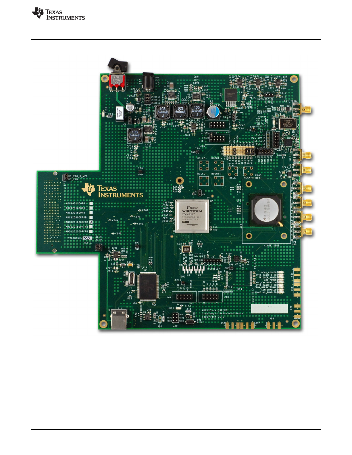
1.4 Board Orientation
Overview
Figure 2. ADC1xDxxxx(RF)RB Board Layout
SNAU146–September 2013 ADC1xDxxxx(RF)RB Reference Board
Submit Documentation Feedback
Copyright © 2013, Texas Instruments Incorporated
5
Page 6
Quick Start
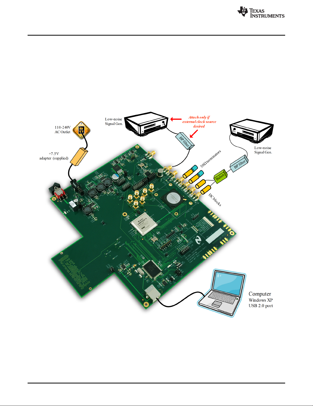
2 Quick Start
This section will aid in bringing up the board for the first time as well as a brief tutorial on the WaveVision
5 (WV5) software. Further description of the Reference Board is in subsequent sections of this document.
The software is further described in the WaveVision 5 Users' Guide or the HELP function within the
software. The ADC1xDxxxx(RF) and LMX2541 data sheets should be consulted for detailed
understanding of device functionality.
The user is advised to construct a lab setup as close to the one shown in Figure 3 as possible. This setup,
along with the board and software configuration described below, is what was used to test the reference
board at Texas Instruments lab. This set of conditions produces the stated reference performance – which
is normally included with each board shipped to customers. The objective is to assure that the user can
achieve the same performance as that recorded at Texas Instruments lab prior to board shipment.
www.ti.com
Figure 3. Recommended Lab Setup. A filter may not be necessary on the clock if the generator is very
clean (beyond –80dBm SFDR).
6
ADC1xDxxxx(RF)RB Reference Board SNAU146–September 2013
Copyright © 2013, Texas Instruments Incorporated
Submit Documentation Feedback
Page 7

www.ti.com
2.1 Installing the WaveVision 5 Software
Note: The WaveVision 5 software will function on Windows 7 and Windows XP 32-bit operating systems.
1. Navigate to the web page:
2. Download the WaveVision5 software to PC or laptop and unzip the file.
3. Run the WV5.exe file.
4. Follow the on-screen instructions to complete the installation.
2.2 Installing the ADC1xDxxxx(RF)RB Hardware
1. Place the ADC1xDxxxx(RF)RB Reference Board on a clean, static-free surface.
2. Connect the enclosed +12V DC power adapter to the power jack. Connect the other side of the power
supply to an AC outlet (100-240 VAC, 50-60 Hz).
3. Connect (but do not yet turn on) the input signal generator, the band-pass filter, the balun and the DC
blocks to the ADC1xDxxxx(RF)RB Reference Board's I-channel input connectors. Set the signal
generator at one of the frequencies and signal levels stated in the reference performance report.
Always use high-quality RF SMA cables for optimum performance.
NOTE: Do not overdrive the signal and clock inputs as the ADC may be damaged. Refer to the
Electrical Specification section of the datasheet for the voltage tolerance of these inputs.
Including insertion loss from filters, baluns, cables, DC blocks, etc. input power should not
exceed operating limits as found in the datasheet.
Quick Start
4. In the Texas Instruments lab, the following (or equivalent performance) equipment are used to test the
board. It is essential that the customer use signal generators, filters, DC blocks and a balun of
equivalent or better performance.
• Rohde & Schwarz SME-03 or SMA-100 signal generator
• Filters - Trilithic 5VF 5% tunable bandpass filter or other fixed frequency bandpass filter of
equivalent performance
• Balun – ADC-LD-BB
• DC blocks – Mini Circuits BLK-89 S+
• 50Ω terminators – Mini Circuits ANNE 50+
Note: The board comes equipped with DC-blocks applied to the I-channel signal input connectors and
DC blocks and terminators applied to the unused Q-channel input connectors. These must be used at
all times - that is, the channel being used must be connected through dc-blocks if the ADC is
configured for ac-coupled operation (as shipped). The unused channel must also be DC blocked then
terminated to ac ground. This is graphically illustrated in Figure 3.
5. Turn on the SW2 rocker power switch. Verify that the red LED (labeled LD10, near the J12 power jack)
is lit.
6. Connect the supplied USB 2.0 cable from the PC USB port to the ADC1xDxxxx(RF)RB USB jack. Note
that the power should be turned on before the USB cable is plugged in.
2.3 Launch the WaveVision 5 Software
Start the WaveVision 5 software on your computer by selecting the desktop icon “WaveVision 5” or by
clicking on the Start button, and selecting
Programs -> WaveVision 5 -> WaveVision 5
The software will automatically detect the board and load the appropriate software profile and will proceed
to download the controller firmware and FPGA code onto the reference board. As an alternative, the icon
on the desktop can be used to launch WaveVision 5. The WaveVision 5 user interface will appear on the
computer screen.
The status LED’s should take on the following states when the system is initially powered up, Wavevision
5 has loaded the FPGA image and the system is ready for an acquisition (where green is on, black is off):
SNAU146–September 2013 ADC1xDxxxx(RF)RB Reference Board
Submit Documentation Feedback
Copyright © 2013, Texas Instruments Incorporated
7
Page 8
DCLK_LOCKED
OVER-RANGE_Q-CH
TRIGGER_ARMED
ADC_POWER
ADC_CALIBRATION
OVER-RANGE_I-CH
ECM_ENABLED
RCOUT1/2_ENABLED
Quick Start
Meaning of the status LED’s:
• DCLK_LOCKED: If FPGA detects DCLKI and DCLKQ toggling, this LED lights. NOTE: If the board
• OVER-RANGE_Q-CH: ADC’s overrange Q-ch pin pulse stretched to around a half second when
• TRIGGER_ARMED: Lights when “H/W Trigger” is checked inside the Wavevision 5 GUI. Does not
• ADC_POWER: Lights when ADC supply voltage of 1.9V is detected.
• ADC_CALIBRATION: Will light temporarily when calibration is run. ADC’s CalRun pin is pulse
• OVER-RANGE_I-CH: ADC’s overrange I-ch pin pulse stretched to around a half second when
• FPGA_OPERATIONAL: Lights when FPGA’s 100MHz reference is locked and FPGA is out of reset.
• ECM_ENABLED: Lights when ADC is in Extended Control Mode.
• RCOUT1/2_ENABLED: Lights when AutoSync RCOUT1/2 clocks are detected. Enabled when
www.ti.com
Figure 4. Note: The status of LED’s are valid, only if the FPGA_OPERATIONAL LED is lit
has been modified for AutoSync to route DCLKQ to the SMA’s, this LED will not be lit.
overranged.
clear upon data capture.
stretched to about a half second.
overranged.
AutoSync-> DOC (disable output clocks) bit is unchecked in Wavevision 5 GUI.
8
ADC1xDxxxx(RF)RB Reference Board SNAU146–September 2013
Copyright © 2013, Texas Instruments Incorporated
Submit Documentation Feedback
Page 9
www.ti.com
2.4 WaveVision 5 - User Interface Overview
Quick Start
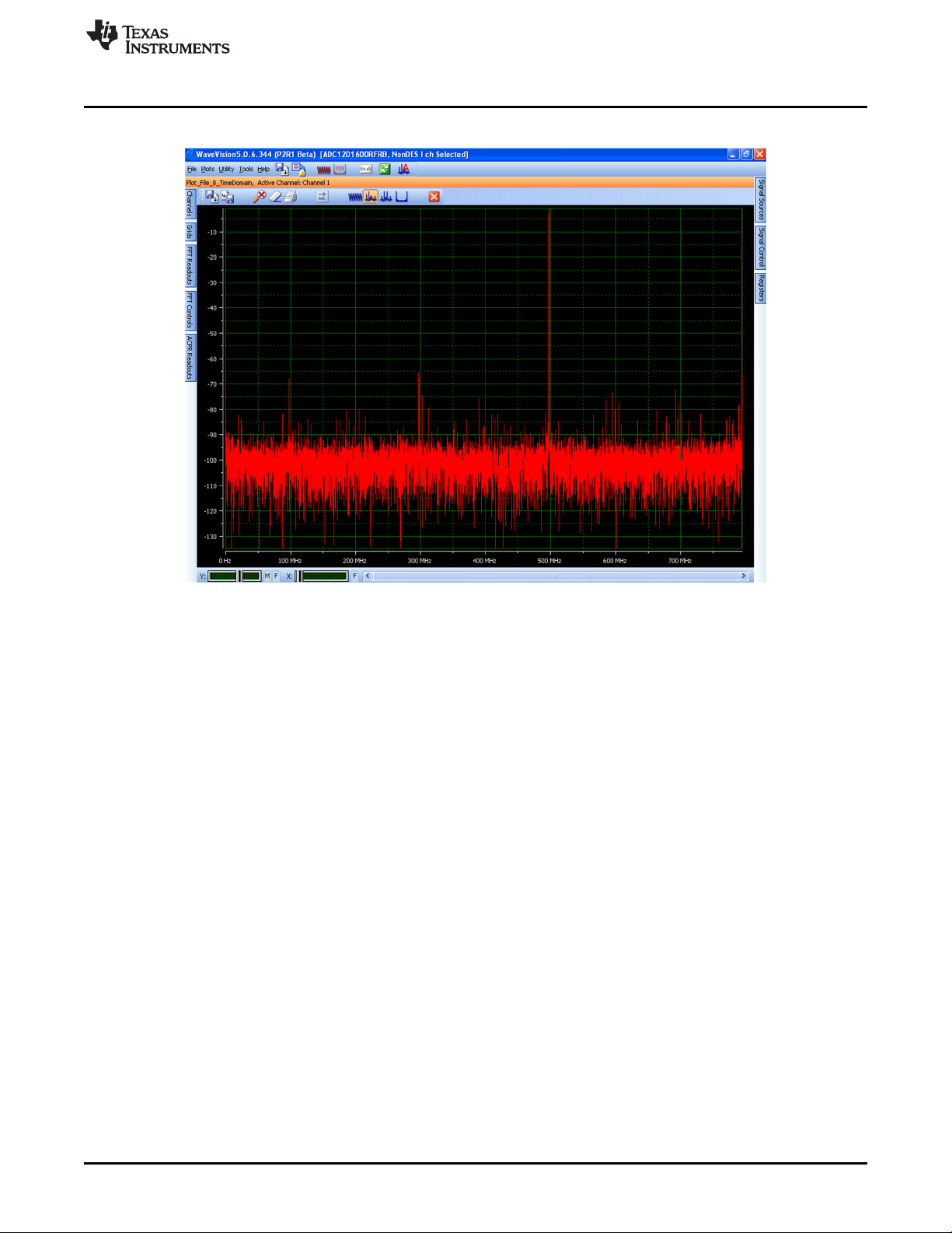
Figure 5. WaveVision 5 Example Window
Figure 5 above shows the WV5 user interface panel (GUI). This is the top level interface panel. It is
arranged in such a way that the plot is always in the middle. There are tabs arranged on each side of the
window to give the user additional information or control of features.
The tabs available on the left side access panels that are pertinent to the current plot window - such as
channel selection, grid selection, FFT Readouts, and FFT controls.
The right side panels allow the user to take control of the hardware. These include the Signal Source,
Signal Control and Registers panels (the most relevant for this board).
In addition, a small FFT parameter summary box can be displayed by pressing CTL-R.
For more details on the general operation and use of WaveVision 5, see the WaveVision 5 Users Guide.
SNAU146–September 2013 ADC1xDxxxx(RF)RB Reference Board
Submit Documentation Feedback
Copyright © 2013, Texas Instruments Incorporated
9
Page 10
Quick Start
2.5 System / Device Configuration
Prior to capturing data, confirm that the board is in the "ECE (Extended Control Enable)" mode, The ECE
jumper is located in the ADC pin control jumper area as shown in Figure 6. The board should be sent with
this jumper in place. This means that the ADC will be controlled through the SPI interface and not with
jumpers driving the control pins. This allows the user to control the ADC's behavior through the
WaveVision 5 Registers panel.
www.ti.com
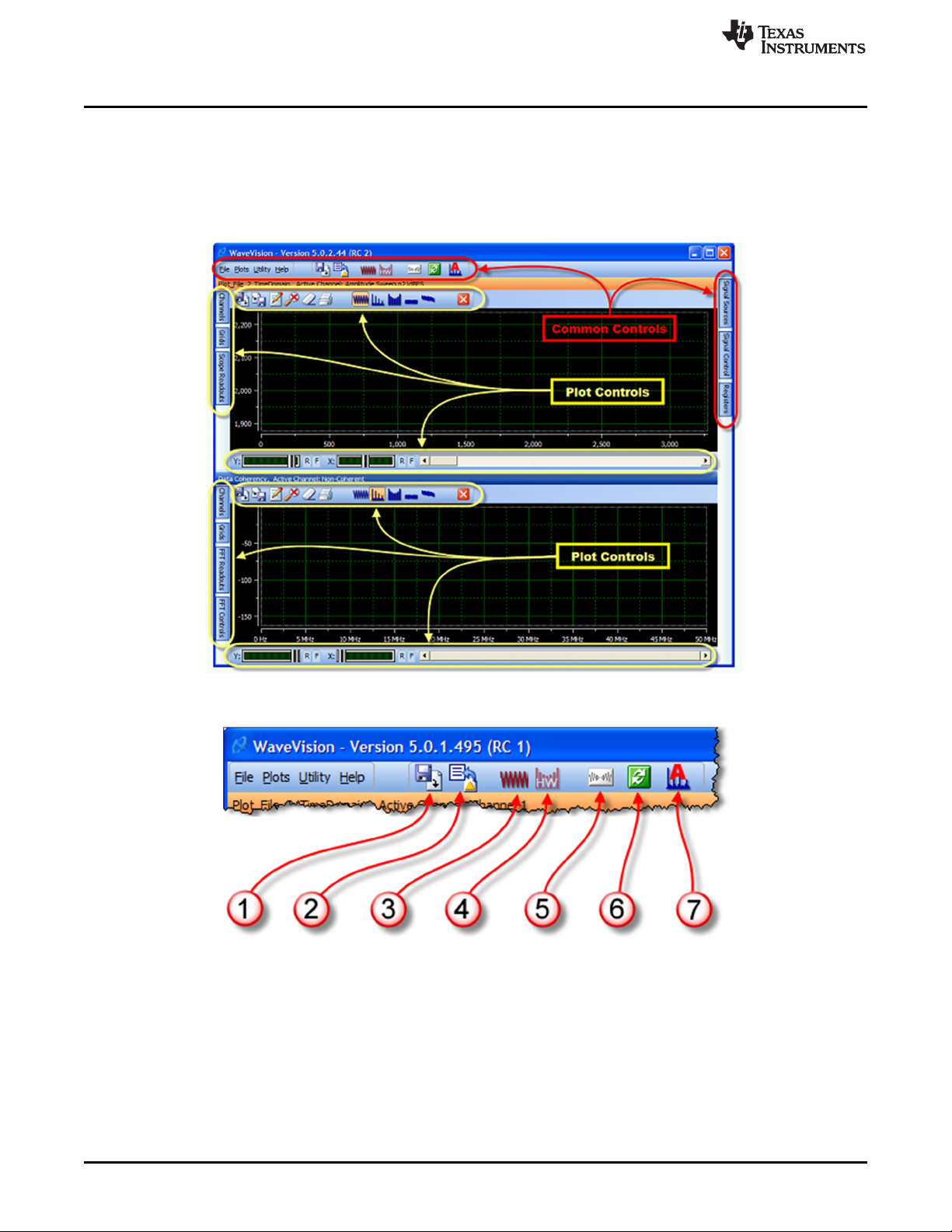
Figure 6. WaveVision 5 overview of control buttons
Figure 7. WaveVision 5 main window command buttons
10
ADC1xDxxxx(RF)RB Reference Board SNAU146–September 2013
Copyright © 2013, Texas Instruments Incorporated
Submit Documentation Feedback
Page 11
www.ti.com
2.5.1 Main Panel
The main menu bar of the WaveVision 5 software has several control buttons as shown in Figure 6 and
Figure 7, which may be used to perform most tasks with a button click.
1 - Load Plot
A new plot window is created and the Plot Load dialog is displayed. The selected plot file is loaded into
the new window.
2 - Import Data
Clicking this button creates a new time-domain plot and opens the Import Data dialog. Data may be
imported from WaveVision 4 data files as well as from ASCII data files created by other programs.
3 - Create a New Time Domain Plot
Clicking this button creates a new time-domain plot. The plot will contain no data, but is available as a
data destination.
4 - Create a New Hardware Histogram Plot
Clicking this button creates a new hardware histogram plot. Hardware histograms are available only in
conjunction with evaluation boards which can gather histogram data internally. This button is enabled
only when an evaluation board which supports hardware histograms is attached.
5 - Acquire Data
Click this button to acquire data to the active plot. If you have created more than one plot, the Active
plot has a highlighted title bar.
6 - Continuous Acquisition
This button is a toggle - when it is pressed, data is acquired continuously, one buffer after another as
fast as the hardware can go; when pressed again data acquisition stops. When in continuous
acquisition mode, acquisition may be started and stopped using the Acquire button without leaving the
continuous acquisition mode.
7 - FFT Averaging
This button is also a toggle - when it is pressed, FFT's are averaged. The number of buffers to be
averaged is specified in the hardware section of the Signal Sources tab.
Please refer to the WaveVision 5 Users Guide for more information.
Quick Start
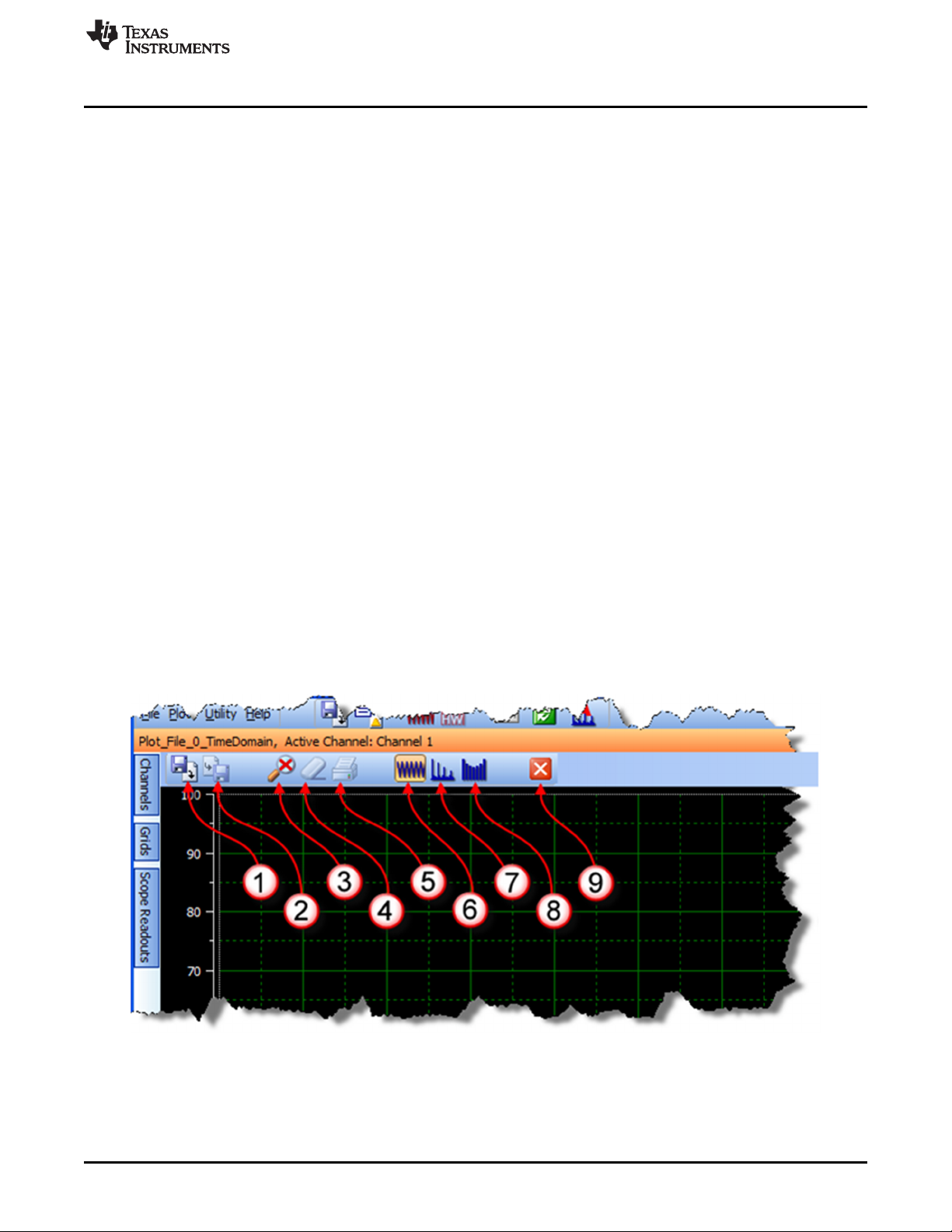
2.5.2 Plot Window Controls
1 - Load Plot
The Plot Load dialog is displayed, and the selected plot file is loaded into the new window.
Figure 8. WaveVision 5 plot window controls
SNAU146–September 2013 ADC1xDxxxx(RF)RB Reference Board
Submit Documentation Feedback
Copyright © 2013, Texas Instruments Incorporated
11
Page 12

Quick Start
2 - Save Plot
Displays the Plot Save dialog (this button is only active when the plot contains one or more channels with
data).
3 - Reset Zoom
Reset X and Y axis zoom to 100%.
4 - Clear
Clear data from all channels.
5 - Print
Print the plot.
6 - Time Domain
Display the plot as time domain data.
7 - FFT
Display the plot as an FFT
8 – Histogram
Display a histogram of the data.
9 - Close
Close this plot.
2.5.3 Right Panels – Signal Source
www.ti.com
12
Figure 9. WaveVision 5 main window command buttons
Open the Signal Source panel on the right side of the window and confirm that the ADC1xDxxxx(RF)RB is
available and confirm that it is selected. There are seven possible modes of operation selectable here:
• NonDES I ch – Dual channel mode capturing and viewing the I-channel data
• NonDES Q ch – Dual channel mode capturing and viewing the Q-channel data
• NonDES I and Q – Dual channel mode capturing and viewing both the I- and Q-channel data
• • DESI Mode – Double Edge Sample (interleaved) mode with I input
ADC1xDxxxx(RF)RB Reference Board SNAU146–September 2013
Copyright © 2013, Texas Instruments Incorporated
Submit Documentation Feedback
Page 13

www.ti.com
• DESQ Mode – Double Edge Sample (interleaved) mode with Q input
• DESIQ Mode – Double Edge Sample (interleaved) mode with I and Q as input – shorts both I and Q
• DESCLKIQ Mode – Sampling Clock samples the I- and Q-channels 180º out of phase with respect to
Double Edge Sampling (DES) – Double edge sampling works much in the same way as single edge
sampling except that the signals is sampled both on the rising and falling edge of the sample clock. This
effectively doubles the sample rate. In this mode, both converters inside the ADC12D1X00RF work on a
common input signal. The various DES modes are selected from the Signal Source tab on the right side
and have requirements for how the inputs must be driven. See the datasheet for more details.
Note: When using “I and Q” mode, it is also necessary to select the Channels tab and deselect the
“Automatically hide inactive channels” option box in order to allow both channels to appear on the plot.
Alternatively, one channel may be displayed per plot:
Quick Start
inputs together and must be externally driven by the same signal
one another – I and Q are not shorted together and must be externally driven by the same signal
Figure 10. I and Q mode – one channel displayed per plot
SNAU146–September 2013 ADC1xDxxxx(RF)RB Reference Board
Submit Documentation Feedback
Copyright © 2013, Texas Instruments Incorporated
13
Page 14

Quick Start
www.ti.com
Figure 11. WaveVision 5 main window command buttons
• Sampling Rate - When the signal source panel is selected, the clock frequency is displayed. This is
initially the internal clock. In this example, 1800 MHz is generated by the LMX2541 on the reference
board. The sampling rate is determined by the FPGA when the board is powered up. The calculation is
accurate to better than 1%. If an external source is in use, confirm that this number corresponds to the
clock reference that is applied. If it is not correct, subsequent data captures and display will not be
correct.
• Resolution – This will always be set to the ADC12D1X00RF resolution which is 12 bits.
• Acquisition Size - This setting displays and selects the number of samples captured in each
acquisition. 4K samples is the default, with settings up to 32K samples. A larger sample size increases
the equivalent FFT bandwidth resolution, but at the expense of more memory and slower acquisition
time.
• Data Format - The default data format is offset binary for the ADC12D1X00RF.
• FFT buffers to average - The last option is the FFT averaging function. Using this feature, subsequent
samples can be averaged to obtain improved signal to noise. However, this is at the expense of time.
2.5.4 Right Panels - Registers
Next, configure the hardware (including the ADC) using the Registers control panel on the right side. This
is the most important of all the panels for controlling the ADC1xDxxxx(RF)RB. This panel has twelve subtabs that control the settings of the board and registers inside the ADC12D1X00RF. The twelve sub-tabs
are shown below and include; Settings, Config, Cal Adjust, I-channel, Q-channel, DES Adjust, tADAdjust,
AutoSync, and Temperature. The last three tabs are register contents so that the user may verify register
settings to be programmed in the system.
14
ADC1xDxxxx(RF)RB Reference Board SNAU146–September 2013
Copyright © 2013, Texas Instruments Incorporated
Submit Documentation Feedback
Page 15

www.ti.com
Quick Start
Figure 12. The top level of the Register panel showing the available tabs
The following is a short description of each tab under the Register panel.
Settings: This tab gives choice of either External Clock or Internal Clock, and buttons to initiate FPGA
Reset, Reset Registers and Calibrate ADC. Calibration of the ADC should be performed if changes occur
such as device temperature, mode changes (single channel to dual channel, single edge sampling (NonDES) to double edge sampling (DES). For more information, refer to the Calibration section of the
ADC12D1X00RF datasheet. The H/W Trigger function is also enabled using the check box on this tab.
Note: If the Internal Clock is selected, then the External Clock signal generator should be disconnected or
switched off to prevent performance degradation.
Config: This tab configures various features and modes of the ADC12D1X00RF and is shown below. It
accesses or changes the following functions, all of which are controlled through Configuration Register 1.
SNAU146–September 2013 ADC1xDxxxx(RF)RB Reference Board
Submit Documentation Feedback
Copyright © 2013, Texas Instruments Incorporated
15
Page 16

Quick Start
www.ti.com
Figure 13. Config Panel
• DPS – DDR Phase Select –
– In DDR, this determines the DDR Data-to-DCLK phase relationship. When unchecked, the 0º Mode
is selected. When checked the 90º Mode is selected.
– In SDR, when this box is unchecked data transitions on the Rising edge of DCLK and when
checked data transitions on the Falling edge of DCLK.
• OVS – Output Voltage Select – Selects the LVDS differential output voltage. When this is unchecked,
the reduced output amplitude is selected. When checked, the standard (higher) output amplitude is
used.
• TPM – Test Pattern Mode – When checked the device will continually output a fixed pattern on the
Data and OR outputs. When cleared, the normal ADC Data and OR information are output.
• PDI – Power down I Channel when checked.
• PDQ – Power down Q channel when checked.
• 2SC – Two’s Complement output mode is selected when checked. Default is offset binary.
• TSE – Check to enable Time Stamp feature.
• SDR – SDR mode when checked; DDR when unchecked. Default is DDR.
Note: Will only work in DDR mode, unless FPGA is changed.
Note: No changes will take effect until the Write Config Reg button is clicked.
Cal Adjust: This tab controls the various adjustments which may be made to the Calibration feature.
16
ADC1xDxxxx(RF)RB Reference Board SNAU146–September 2013
Copyright © 2013, Texas Instruments Incorporated
Submit Documentation Feedback
Page 17

www.ti.com
Quick Start
Figure 14. Cal Adjust Panel
• CSS – Skip or include Rtrim calibration. When the Rtrim has been completed once, it is not necessary
to do it again until the device is power cycled.
• SSC – Calibration control via the SPI, i.e. not the pin-controlled option for calibration.
Note: No changes will take effect until the Write Config Reg button is clicked.
I-channel: This tab changes the sign and the magnitude of the offset and the full scale range settings.
SNAU146–September 2013 ADC1xDxxxx(RF)RB Reference Board
Submit Documentation Feedback
Copyright © 2013, Texas Instruments Incorporated
17
Page 18

Quick Start
www.ti.com
Figure 15. I-Channel Panel
• I-channel Offset Sign – This pull-down selects a positive or negative offset.
• I-ch Offset – This slider selects the magnitude of I-ch Offset applied. Adjustment can be done using
the computer mouse/pointer, or using left/right arrow keys once the slider has been selected. Although
the offset is entered in a 10 bit (0 to 4095) relative form, it is also displayed in approximate mV.
• I-Channel Full Scale - The approximate I-Channel input full scale range (mV peak-to-peak) is
selected, ranging from a minimum of 600mV to a maximum of 1000mV. The default setting is 800mV.
Note: No changes will take effect until the Write I-ch Reg button is clicked. Also, the ADC must be recalibrated if the full-scale is changed.
Q-channel: Similar to I-channel
DES Adjust: This tab controls the DES Mode time skew function.
18
ADC1xDxxxx(RF)RB Reference Board SNAU146–September 2013
Copyright © 2013, Texas Instruments Incorporated
Submit Documentation Feedback
Page 19

www.ti.com
Quick Start
Figure 16. DES Adjust Panel
Set DES Mode time skew – This slider adjusts the time skew between the falling edge sampling clock
relative to the rising edge sampling clock in DES mode. Adjustment can be done using the computer
mouse/pointer, or using left/right arrow keys once the slider has been selected. Although the time skew is
entered in 8 bit (0 to 127) relative form, it is also displayed in approximate fs.
Note: No changes will take effect until the Write Reg button is clicked.
tADAdjust: This tab controls the Aperture Delay function.
SNAU146–September 2013 ADC1xDxxxx(RF)RB Reference Board
Submit Documentation Feedback
Copyright © 2013, Texas Instruments Incorporated
19
Page 20

Quick Start
www.ti.com
Figure 17. tADAdjust Panel
• DCC – Duty Cycle Correction – When checked (default), the automatic Duty Cycle Correction circuit is
enabled.
• STA - Select tAD Adjust – When checked, enables the Aperture Delay Time coarse adjust feature.
• Coarse Phase Adjust – Sets the approximate amount of coarse Aperture Delay applied.
• Fine Phase Adjust – Sets the approximate amount of fine Aperture Delay applied.
• SA – Select tAD Adjust – When checked, enables the Aperture Delay Time fine adjust feature.
(Overrides the STA function)
Note: No changes will take effect until the Write Adjust Reg button is clicked.
AutoSync: This tab enables and controls the settings of the AutoSync feature.
20
ADC1xDxxxx(RF)RB Reference Board SNAU146–September 2013
Copyright © 2013, Texas Instruments Incorporated
Submit Documentation Feedback
Page 21

www.ti.com
Quick Start
Figure 18. AutoSync Panel
• DR – Disable DCLK Reset – When checked (default) disables the DCLK Reset feature
• DOC - Disable Output reference Clocks – When checked (default) disables the AutoSync reference
output clocks. When un-checked a CLK/4 signal is sent on the RCOut1 and RCOut2 outputs.
• ES – Enable Slave mode – When checked configures this ADC as an AutoSync slave device.
• Select Phase – Selects the Phase of the incoming reference clock used by the AutoSync feature.
• Reference Clock Delay – This selects the additional delay added to the input reference clock.
Settings are 0d (0s) to 319d (1000ps). Settings higher than 319d will give 1000ps delay.
Note: No changes will take effect until the Write AutoSync Reg button is clicked.
Temperature: This panel provides a read-out of three different temperatures in the ADC1xDxxxx(RF)RB.
SNAU146–September 2013 ADC1xDxxxx(RF)RB Reference Board
Submit Documentation Feedback
Copyright © 2013, Texas Instruments Incorporated
21
Page 22

Quick Start
www.ti.com
Figure 19. Temperature Panel
• Ambient Temperature – Provides the local/board temperature of the LM95233 IC.
• ADC Temperature – Provides the approximate die temperature of the ADC12D1X00RF.
• FPGA Temperature – Provides the approximate die temperature of the Xilinx Virtex-4 FPGA.
Note: No changes will appear until the Update Temperatures button is clicked.
Debug Tabs: These panels provide the actual register settings which are conveniently formatted in the
other tabs above. They may also be read to and written from and these changes will be reflected in the
corresponding tabs.
22
ADC1xDxxxx(RF)RB Reference Board SNAU146–September 2013
Copyright © 2013, Texas Instruments Incorporated
Submit Documentation Feedback
Page 23

www.ti.com
Quick Start
Note: No changes will appear until the Read/Write button is clicked.
NOTE: Register 6h must be programmed to 1C0Eh before calibrating for the ADC12D1800RF to
function properly. This is accomplished automatically via the GUI programming for the
ADC12D1800RF Reference Board, and in the customer’s system, it must also be
programmed.
2.6 Data Capturing
The board is now ready for a data capture. Before proceeding, perform a manual calibration of the ADC.
Even though the ADC performs a self-calibration at the time of power-up, it is recommended that the user
perform another calibration after sufficient time has passed for the system (primarily temperature) to
stabilize. Manual calibration is performed by clicking the Calibrate ADC feature in the Register control
panel, Settings sub-tab.
2.6.1 Configure Display Settings
Open the FFT Control left panel. Confirm that the dBFS unit is selected. Also confirm that the correct clock
frequency is being measured by the software by checking in the Signal Source right panel. The default
frequency of the on-board clock source is shown in the board performance data shipped with your board.
2.6.2 Check Input Amplitude
Confirm that the Over-range LEDs are not illuminated. Now increase the signal amplitude until the LED for
the input in use is just barely lit. DO NOT increase signal power much beyond this point as the ADC's
inputs can be damaged if the Operating Maximums are exceeded (see Electrical Specification section).
Then reduce the signal amplitude until the Over-range LED is no longer illuminated. You should now have
an input signal that is very close to the ADC's full-scale range (e.g., within 0.5 to 1.0 dB).
Figure 20. Debug Panel
SNAU146–September 2013 ADC1xDxxxx(RF)RB Reference Board
Submit Documentation Feedback
Copyright © 2013, Texas Instruments Incorporated
23
Page 24

Secondary Panel Description
IMPORTANT: Since the ADC signal and clock inputs are not provided with additional protection
circuitry on this board, the burden is on the user to not overdrive the inputs to the extent of
damaging them. An "Over-range" LED is provided for each channel to indicate that the signal
amplitude is beyond the ADC full-scale range. Keep the signal amplitude within the operating
ratings as specified in the datasheet. Thus, the safe method of setting the signal amplitude to fullscale level is to utilize the LED as described in the previous paragraph to roughly obtain the fullscale amplitude and then inspect the captured data in the software's time-domain plot to fine tune
the amplitude to the desired level.
2.6.3 Acquire and Display Data
Perform a data acquisition by clicking the Acquire Data button (Item #5 in Figure 7). The acquired data will
now appear in the (default) time domain plot window. Switch to the frequency-domain window (FFT) using
the WaveVision 5 controls. Type Ctrl-r to obtain the summary of the acquisition. Place the software in
continuous mode (Item #6 of Figure 7) and then acquire again. This is to confirm that the Over-range LED
method used earlier indeed gave a signal to the ADC that is within –0.5 to –1.0 dB of the full-scale range.
If not, adjust the input signal generator's signal power to approximately –0.5dB of full scale.
At this point, dynamic performance metrics similar to those shown on the reference data shipped with the
board may be obtained. One of the basic variables that you may experiment with at this point is to change
the input signal strength and frequency. Please note that to achieve the reference performance, bandpass filters similar to the items referenced in Section 2.2 should be used. The absence of these filters on
the input signal or external clock will usually result in sub-standard performance.
The displayed units should be in dBFS as selected earlier. You may switch the units to dBc and back to
dBFS as desired.
www.ti.com
2.6.4 It is also possible to apply a high-quality external signal source to the clock input rather than using the on-board LMX2541 clock synthesizer. This will help quantify the LMX2541's performance in an ultrahigh-speed signal-path such as this one. When connecting an external clock source, the generator amplitude should be set to 0dBm. Experiment with the clock signal strength to determine what effect this has on the channel performance. Care should be taken to not exceed +4 dBm at the clock input, to avoid damage to the ADC.
The external clock source is enabled through the register control panel in the software after applying the
signal generator to the Clock input SMA.
The external clock source should be disconnected or turned off when the on-board clock source is
selected. Failure to do so will result in poor performance due to the mixing of the on-board clock
and the small amount of external clock signal leaking through the clock selection relay.
It is important to keep in mind that if the ADC's operating conditions are changed in any significant way,
especially temperature, the ADC should be calibrated again before proceeding.
Please refer to the WaveVision 5 Users' Guide and integral Help feature for more information concerning
the software.
3 Secondary Panel Description
Please refer to the WaveVision 5 Users Guide for detailed descriptions of the remaining Left and Right
panels, and additional Main Panel features.
24
ADC1xDxxxx(RF)RB Reference Board SNAU146–September 2013
Copyright © 2013, Texas Instruments Incorporated
Submit Documentation Feedback
Page 25

ADC12D1X00RF
Clk Gen
(LMX2531)
USB
Ctrlr.
USB
Xilinx
Virtex
- 4 FPGA
Power Management
12x2
12x2
Ext Clock
DCLK_RST
VinI+/
-
VinQ+/
-
SE2DIFF
Analog_3.3V
Digital_3.3V
Analog_1.9V
7.5V
EEPROM
Local Clock
(96 MHz)
DCLKI/Q
SPI(1.8V)
USI - 1 Conx.x2 for
external devices
Vcmo
Analog Front
-
End
Boards Plug
-
in Here
(LMH6518, Balun, RF)
Digital_2.5V
Digital_1.8V
Digital_1.2V
+3.3V/5V,
GND
Analog_3.3/5.0V
(for off
-
board use)
Vreg
+5V
+3.3V
Power
Sequencing
Control
Temp Sensor
(LM95233)
I2C
ADR/DATA
FIFO I/F
uWire
SPI(3.3V)
SE2DIFF
Trigger
SE2DIFF
ORI/Q
2
2
www.ti.com
4 Reference Board Functional Description
4.1 System Block Diagram
Reference Board Functional Description
4.2 System Description
4.2.1 The ADC12D1X00RF
SNAU146–September 2013 ADC1xDxxxx(RF)RB Reference Board
Submit Documentation Feedback
Figure 21. ADC1xDxxxx(RF)RB System Block Diagram
ADC12D1X00RF forms the heart of this reference board. This low-power, high-performance CMOS
analog-to-digital converter digitizes signals at 12-bit resolution at guaranteed minimum sampling rates of
1.6/1.8 Gs/s in dual channel configuration and 3.2/3.6 Gs/s in single channel configuration. The
ADC12D1X00RF is targeted at achieving very good accuracy and dynamic performance while consuming
the lowest power available in the industry when both channels are powered-up. The product is packaged
in a thermally enhanced BGA package that does not require a heat sink over the rated ambient
temperature range of –40º C to +70º C. Refer to the latest version of the ADC12D1X00RF datasheet for
more detailed information.
Copyright © 2013, Texas Instruments Incorporated
25
Page 26

Reference Board Functional Description
This reference board gives complete control over the ADC12D1X00RF and gives the user direct
performance results of the chip without the need for an elaborate setup. Each of the device's control pins
may be set high or low. Control is provided in two different manners - direct pin control with jumpers or
through the serial interface (the device's extended control mode) using the WV 5 register control panel. In
order to use the extended control mode the ECE jumper must be set to LOW. This is the recommended
method and gives the user the most flexibility and ease of use.
Analog Front-End: The analog signal connection to the ADC is kept simple on this board in order to
achieve the highest possible bandwidth. The board is designed to be coupled to front-end circuitry in a DC
or AC coupled manner. AC-coupling requires the use of dc-blocks on the SMA connectors. By default, the
board is shipped by Texas Instruments with dc-blocks. In addition, the board is also jumper-configured for
DC-coupled operation (pin 9 on J15 is removed for DC operation).
Multi-channel ADC synchronization: A DCLK_RST signal input is provided to synchronize the ADCs on
multiple boards or systems. In addition, the ADC12D1X00RF supports a new method of ADC
synchronization, called AutoSync. Please refer to the ADC12D1X00RF datasheet for more details.
4.2.2 LMX2541 Clock Synthesis chip
The LMX2541xxxx family provides a single-chip, very low-jitter clock solution at frequencies up to 2.0
GHz. In this application, the LMX2541LQ1570E / LMX2541LQ1778E is used - which can be programmed
to operate over a range of 1530-1636MHz / 1726-1840MHz. On the ADC1xDxxxx(RF)RB board, the
device is configured for a frequency in this range through the serial interface which may be controlled
through the WaveVision 5 register control panel. The particular frequency chosen is one that generates
the least phase noise. It is not necessarily a round number but depends on the loop feedback of the PLL’s
in the clock synthesis chip.
The clock source for the ADC can be selected between the on-board LMX2541 or an external clock
source connected through the J11 SMA connector. The selection is performed through the WV 5 register
panel. It is recommended that the external clock source should be connected and enabled before it is
selected. For optimum performance, the external clock signal generator and the LMX2541 should
not be enabled at the same time. This is because the RF relay used to select between them does not
provide adequate isolation to keep one from affecting the other. Having both clocks on simultaneously will
result in excessive spurious signals. The default setting for this board is the on-board LMX2541 clock
source.
www.ti.com
4.2.3 FPGA
The design employs a Xilinx Virtex-4 FPGA for capturing the digital data. While the board is powered up
and configured, the FPGA is continually receiving data from the ADC. In response to a user command
through the WV-5 software, the ADC captures the desired amount of data in its on-chip buffer (up to a
maximum of 32K samples per-channel). The user can then command the FPGA to upload the captured
data to the PC through the USB interface for further processing.
This board can support the ability to program the FPGA for specific requirements. A standard JTAG
connector is provided for downloading FPGA object code from the Xilinx development environment.
Please note that Texas Instruments does not provide support for any user-designed FPGA functionality
beyond the standard functionality that is shipped with the board.
Hardware Trigger: The external trigger feature of the Reference Board is designed to enable applications
which trigger a data capture. When the hardware trigger is enabled, an acquisition can be selected from
the software, but the actual beginning of data capture will be postponed until the external trigger pulse is
applied to the J26, the EXT_TRIG SMA.
Note: This only applies to the data which is captured and displayed in the WaveVision GUI; the streaming
data to the FMC connector still runs continuously.
26
ADC1xDxxxx(RF)RB Reference Board SNAU146–September 2013
Copyright © 2013, Texas Instruments Incorporated
Submit Documentation Feedback
Page 27

Mezzanine
(ADC12D1X00RFRB)
Carrier
FMC_PG_M2C
J156
Override power
good M2C (indicates
power good from
Mez. to Carrier)
J155
Override power
good C2M
(FPGA will
output data on
FMC)
FMC_PG_C2M
www.ti.com
Apply the trigger signal at J26, the EXT_TRIG SMA. If the voltage applied, Vtrigger is less than the
threshold, Vth, of the MC100EP16, then the system will not capture. If Vtrigger is greater than Vth, then a
data capture will occur. Vth is approximately 2.1V, so it is recommended that high trigger voltage is in the
range of {2.5V, 3.3V}. The low trigger voltage should be 0V. Note that this may be a single shot data
capture or a continuous trigger. If the trigger is armed, but Vtrigger is not greater than Vth within
approximately 3 minutes, then the software will time out and show the error message: “Board failed to
collect samples.”
Reference Board Functional Description
1. Connect a signal source to the EXT_TRIG SMA (J26).
2. In the WaveVision5 GUI, select Registers – Settings – check the H/W Trigger box.
3. Select single or continuous capture.
4. Apply Vtrigger above the threshold, Vth, when ready to capture.
Auxiliary Port: FMC connector forms an auxiliary data port. With it, the FPGA captures the ADC’s high-
speed continuous streaming data and retransmits the data out of the FMC port. See photo below of the
FMC port on the bottom of the board.
• Install J155 to force FPGA to output data on FMC port (without a power good signal from Carrier to
• Install J156 to force a power good signal from Mezzanine (ADC12D1X000RFRB) to Carrier. This is
SNAU146–September 2013 ADC1xDxxxx(RF)RB Reference Board
Submit Documentation Feedback
Figure 22. Trigger circuit on reference board
Mezzanine). This is useful when a non FMC compliant board is connected to Mezzanine
(ADC1xDxxxx(RF)RB)
used to override for initial FPGA debug.
Figure 23. Explanation of Power Good override jumpers for FMC port
Copyright © 2013, Texas Instruments Incorporated
27
Page 28

Reference Board Functional Description
www.ti.com
28
Figure 24. Bottom of ADC1xDxxxx(RF)RB showing FMC port
AutoSync SMA connectors: Needs resistor jumper modification to evaluate AutoSync on the reference
board. See schematic to find the resistor locations.
• Remove DCLKQ+/-, RCOUT1+/- to FPGA (Remove R162, R163, R158, R159)
• Route DCLKQ+/-, RCOUT1+/-, RCLK+/- to SMA connectors (Stuff 0ohm resistors to R161, R164,
R157, R160, R145, R147)
Enable AutoSync output by going to Wavevision 5 Software GUI -> Registers tab -> AutoSync panel ->
Uncheck DOC and click ‘Write AutoSync Reg’. Notice that LED RCOUT1/2_ENABLED will light and
DCLK_LOCKED will not light.
ADC1xDxxxx(RF)RB Reference Board SNAU146–September 2013
Copyright © 2013, Texas Instruments Incorporated
Submit Documentation Feedback
Page 29

Rclk
Ref
SigGen
Fclk
SigGen
Rclk=Fclk/4
ADC in Autosync
Slave Mode
www.ti.com
The board has SMA connectors for DCLKQ+, DCLKQ-, RCOUT1+, RCOUT1-, RCLK+, RCLK- on the
board. See the ADC12D1X00RF datasheet and Application Note 2132 for details on how to use the
AutoSync feature.
For example, one reference board can be configured in Slave Mode and its RCLK driven externally by a
signal generator which is phase locked to the sampling clock. For this setup, the Reference Board must
select the EXT CLK. The DCLK and RCOut1 may be conveniently monitored via the on-board SMA
connectors for exploration of the AutoSync feature.
Electrical Specifications
Figure 25. AutoSync example with one reference board in slave mode
4.2.4 LM95233 Temperature Sensor
Using the Texas Instruments LM95233 temp sensor chip; the ambient, ADC12D1X00RF and Xilinx FPGA
temperatures can be monitored. The temperature readings are available through the WV-5 software.
5 Electrical Specifications
Power Supply: Minimum = 11V, Maximum = 13V
Power Consumption:
ADC Input Signals: (The maximum level at the signal generator is dependent upon the insertion loss from
Clock Input Signal: (The maximum level at the signal generator is dependent upon the insertion loss from
USB Port: USB 2.0 compliant
Table 2. Electrical Specifications
Nominal = 12V
(Voltages outside these levels will cause damage!!)
Nominal = 10 Watts
Maximum = 20 Watts
Maximum Operating Voltage = see datasheet
Recommended/initial (full scale) generator setting = 0 dBm
other hardware before the ADC inputs. Care should be taken not to exceed the
Operating Ratings at the ADC input).
Maximum Operating Voltage = +2.0V
Recommended generator setting = +1 dBm
other hardware before the clock inputs. Care should be taken not to exceed the
maximum limits at the clock inputs).
SNAU146–September 2013 ADC1xDxxxx(RF)RB Reference Board
Submit Documentation Feedback
Copyright © 2013, Texas Instruments Incorporated
29
Page 30

EVALUATION BOARD/KIT/MODULE (EVM) ADDITIONAL TERMS
Texas Instruments (TI) provides the enclosed Evaluation Board/Kit/Module (EVM) under the following conditions:
The user assumes all responsibility and liability for proper and safe handling of the goods. Further, the user indemnifies TI from all claims
arising from the handling or use of the goods.
Should this evaluation board/kit not meet the specifications indicated in the User’s Guide, the board/kit may be returned within 30 days from
the date of delivery for a full refund. THE FOREGOING LIMITED WARRANTY IS THE EXCLUSIVE WARRANTY MADE BY SELLER TO
BUYER AND IS IN LIEU OF ALL OTHER WARRANTIES, EXPRESSED, IMPLIED, OR STATUTORY, INCLUDING ANY WARRANTY OF
MERCHANTABILITY OR FITNESS FOR ANY PARTICULAR PURPOSE. EXCEPT TO THE EXTENT OF THE INDEMNITY SET FORTH
ABOVE, NEITHER PARTY SHALL BE LIABLE TO THE OTHER FOR ANY INDIRECT, SPECIAL, INCIDENTAL, OR CONSEQUENTIAL
DAMAGES.
Please read the User's Guide and, specifically, the Warnings and Restrictions notice in the User's Guide prior to handling the product. This
notice contains important safety information about temperatures and voltages. For additional information on TI's environmental and/or safety
programs, please visit www.ti.com/esh or contact TI.
No license is granted under any patent right or other intellectual property right of TI covering or relating to any machine, process, or
combination in which such TI products or services might be or are used. TI currently deals with a variety of customers for products, and
therefore our arrangement with the user is not exclusive. TI assumes no liability for applications assistance, customer product design,
software performance, or infringement of patents or services described herein.
REGULATORY COMPLIANCE INFORMATION
As noted in the EVM User’s Guide and/or EVM itself, this EVM and/or accompanying hardware may or may not be subject to the Federal
Communications Commission (FCC) and Industry Canada (IC) rules.
For EVMs not subject to the above rules, this evaluation board/kit/module is intended for use for ENGINEERING DEVELOPMENT,
DEMONSTRATION OR EVALUATION PURPOSES ONLY and is not considered by TI to be a finished end product fit for general consumer
use. It generates, uses, and can radiate radio frequency energy and has not been tested for compliance with the limits of computing
devices pursuant to part 15 of FCC or ICES-003 rules, which are designed to provide reasonable protection against radio frequency
interference. Operation of the equipment may cause interference with radio communications, in which case the user at his own expense will
be required to take whatever measures may be required to correct this interference.
General Statement for EVMs including a radio
User Power/Frequency Use Obligations: This radio is intended for development/professional use only in legally allocated frequency and
power limits. Any use of radio frequencies and/or power availability of this EVM and its development application(s) must comply with local
laws governing radio spectrum allocation and power limits for this evaluation module. It is the user’s sole responsibility to only operate this
radio in legally acceptable frequency space and within legally mandated power limitations. Any exceptions to this are strictly prohibited and
unauthorized by Texas Instruments unless user has obtained appropriate experimental/development licenses from local regulatory
authorities, which is responsibility of user including its acceptable authorization.
For EVMs annotated as FCC – FEDERAL COMMUNICATIONS COMMISSION Part 15 Compliant
Caution
This device complies with part 15 of the FCC Rules. Operation is subject to the following two conditions: (1) This device may not cause
harmful interference, and (2) this device must accept any interference received, including interference that may cause undesired operation.
Changes or modifications not expressly approved by the party responsible for compliance could void the user's authority to operate the
equipment.
FCC Interference Statement for Class A EVM devices
This equipment has been tested and found to comply with the limits for a Class A digital device, pursuant to part 15 of the FCC Rules.
These limits are designed to provide reasonable protection against harmful interference when the equipment is operated in a commercial
environment. This equipment generates, uses, and can radiate radio frequency energy and, if not installed and used in accordance with the
instruction manual, may cause harmful interference to radio communications. Operation of this equipment in a residential area is likely to
cause harmful interference in which case the user will be required to correct the interference at his own expense.
Page 31

FCC Interference Statement for Class B EVM devices
This equipment has been tested and found to comply with the limits for a Class B digital device, pursuant to part 15 of the FCC Rules.
These limits are designed to provide reasonable protection against harmful interference in a residential installation. This equipment
generates, uses and can radiate radio frequency energy and, if not installed and used in accordance with the instructions, may cause
harmful interference to radio communications. However, there is no guarantee that interference will not occur in a particular installation. If
this equipment does cause harmful interference to radio or television reception, which can be determined by turning the equipment off and
on, the user is encouraged to try to correct the interference by one or more of the following measures:
• Reorient or relocate the receiving antenna.
• Increase the separation between the equipment and receiver.
• Connect the equipment into an outlet on a circuit different from that to which the receiver is connected.
• Consult the dealer or an experienced radio/TV technician for help.
For EVMs annotated as IC – INDUSTRY CANADA Compliant
This Class A or B digital apparatus complies with Canadian ICES-003.
Changes or modifications not expressly approved by the party responsible for compliance could void the user’s authority to operate the
equipment.
Concerning EVMs including radio transmitters
This device complies with Industry Canada licence-exempt RSS standard(s). Operation is subject to the following two conditions: (1) this
device may not cause interference, and (2) this device must accept any interference, including interference that may cause undesired
operation of the device.
Concerning EVMs including detachable antennas
Under Industry Canada regulations, this radio transmitter may only operate using an antenna of a type and maximum (or lesser) gain
approved for the transmitter by Industry Canada. To reduce potential radio interference to other users, the antenna type and its gain should
be so chosen that the equivalent isotropically radiated power (e.i.r.p.) is not more than that necessary for successful communication.
This radio transmitter has been approved by Industry Canada to operate with the antenna types listed in the user guide with the maximum
permissible gain and required antenna impedance for each antenna type indicated. Antenna types not included in this list, having a gain
greater than the maximum gain indicated for that type, are strictly prohibited for use with this device.
Cet appareil numérique de la classe A ou B est conforme à la norme NMB-003 du Canada.
Les changements ou les modifications pas expressément approuvés par la partie responsable de la conformité ont pu vider l’autorité de
l'utilisateur pour actionner l'équipement.
Concernant les EVMs avec appareils radio
Le présent appareil est conforme aux CNR d'Industrie Canada applicables aux appareils radio exempts de licence. L'exploitation est
autorisée aux deux conditions suivantes : (1) l'appareil ne doit pas produire de brouillage, et (2) l'utilisateur de l'appareil doit accepter tout
brouillage radioélectrique subi, même si le brouillage est susceptible d'en compromettre le fonctionnement.
Concernant les EVMs avec antennes détachables
Conformément à la réglementation d'Industrie Canada, le présent émetteur radio peut fonctionner avec une antenne d'un type et d'un gain
maximal (ou inférieur) approuvé pour l'émetteur par Industrie Canada. Dans le but de réduire les risques de brouillage radioélectrique à
l'intention des autres utilisateurs, il faut choisir le type d'antenne et son gain de sorte que la puissance isotrope rayonnée équivalente
(p.i.r.e.) ne dépasse pas l'intensité nécessaire à l'établissement d'une communication satisfaisante.
Le présent émetteur radio a été approuvé par Industrie Canada pour fonctionner avec les types d'antenne énumérés dans le manuel
d’usage et ayant un gain admissible maximal et l'impédance requise pour chaque type d'antenne. Les types d'antenne non inclus dans
cette liste, ou dont le gain est supérieur au gain maximal indiqué, sont strictement interdits pour l'exploitation de l'émetteur.
SPACER
SPACER
SPACER
SPACER
SPACER
SPACER
SPACER
SPACER
Page 32

【【Important Notice for Users of EVMs for RF Products in Japan】】
This development kit is NOT certified as Confirming to Technical Regulations of Radio Law of Japan
If you use this product in Japan, you are required by Radio Law of Japan to follow the instructions below with respect to this product:
1. Use this product in a shielded room or any other test facility as defined in the notification #173 issued by Ministry of Internal Affairs and
Communications on March 28, 2006, based on Sub-section 1.1 of Article 6 of the Ministry’s Rule for Enforcement of Radio Law of
Japan,
2. Use this product only after you obtained the license of Test Radio Station as provided in Radio Law of Japan with respect to this
product, or
3. Use of this product only after you obtained the Technical Regulations Conformity Certification as provided in Radio Law of Japan with
respect to this product. Also, please do not transfer this product, unless you give the same notice above to the transferee. Please note
that if you could not follow the instructions above, you will be subject to penalties of Radio Law of Japan.
(address) 24-1, Nishi-Shinjuku 6 chome, Shinjuku-ku, Tokyo, Japan
http://www.tij.co.jp
【無線電波を送信する製品の開発キットをお使いになる際の注意事項】
本開発キットは技術基準適合証明を受けておりません。
本製品のご使用に際しては、電波法遵守のため、以下のいずれかの措置を取っていただく必要がありますのでご注意ください。
1. 電波法施行規則第6条第1項第1号に基づく平成18年3月28日総務省告示第173号で定められた電波暗室等の試験設備でご使用いただく。
2. 実験局の免許を取得後ご使用いただく。
3. 技術基準適合証明を取得後ご使用いただく。
なお、本製品は、上記の「ご使用にあたっての注意」を譲渡先、移転先に通知しない限り、譲渡、移転できないものとします。
上記を遵守頂けない場合は、電波法の罰則が適用される可能性があることをご留意ください。
日本テキサス・インスツルメンツ株式会社
東京都新宿区西新宿6丁目24番1号
西新宿三井ビル
http://www.tij.co.jp
Texas Instruments Japan Limited
SPACER
SPACER
SPACER
SPACER
SPACER
SPACER
SPACER
SPACER
SPACER
SPACER
SPACER
SPACER
SPACER
SPACER
SPACER
SPACER
SPACER
Page 33

EVALUATION BOARD/KIT/MODULE (EVM)
WARNINGS, RESTRICTIONS AND DISCLAIMERS
For Feasibility Evaluation Only, in Laboratory/Development Environments. Unless otherwise indicated, this EVM is not a finished
electrical equipment and not intended for consumer use. It is intended solely for use for preliminary feasibility evaluation in
laboratory/development environments by technically qualified electronics experts who are familiar with the dangers and application risks
associated with handling electrical mechanical components, systems and subsystems. It should not be used as all or part of a finished end
product.
Your Sole Responsibility and Risk. You acknowledge, represent and agree that:
1. You have unique knowledge concerning Federal, State and local regulatory requirements (including but not limited to Food and Drug
Administration regulations, if applicable) which relate to your products and which relate to your use (and/or that of your employees,
affiliates, contractors or designees) of the EVM for evaluation, testing and other purposes.
2. You have full and exclusive responsibility to assure the safety and compliance of your products with all such laws and other applicable
regulatory requirements, and also to assure the safety of any activities to be conducted by you and/or your employees, affiliates,
contractors or designees, using the EVM. Further, you are responsible to assure that any interfaces (electronic and/or mechanical)
between the EVM and any human body are designed with suitable isolation and means to safely limit accessible leakage currents to
minimize the risk of electrical shock hazard.
3. Since the EVM is not a completed product, it may not meet all applicable regulatory and safety compliance standards (such as UL,
CSA, VDE, CE, RoHS and WEEE) which may normally be associated with similar items. You assume full responsibility to determine
and/or assure compliance with any such standards and related certifications as may be applicable. You will employ reasonable
safeguards to ensure that your use of the EVM will not result in any property damage, injury or death, even if the EVM should fail to
perform as described or expected.
4. You will take care of proper disposal and recycling of the EVM’s electronic components and packing materials.
Certain Instructions. It is important to operate this EVM within TI’s recommended specifications and environmental considerations per the
user guidelines. Exceeding the specified EVM ratings (including but not limited to input and output voltage, current, power, and
environmental ranges) may cause property damage, personal injury or death. If there are questions concerning these ratings please contact
a TI field representative prior to connecting interface electronics including input power and intended loads. Any loads applied outside of the
specified output range may result in unintended and/or inaccurate operation and/or possible permanent damage to the EVM and/or
interface electronics. Please consult the EVM User's Guide prior to connecting any load to the EVM output. If there is uncertainty as to the
load specification, please contact a TI field representative. During normal operation, some circuit components may have case temperatures
greater than 60°C as long as the input and output are maintained at a normal ambient operating temperature. These components include
but are not limited to linear regulators, switching transistors, pass transistors, and current sense resistors which can be identified using the
EVM schematic located in the EVM User's Guide. When placing measurement probes near these devices during normal operation, please
be aware that these devices may be very warm to the touch. As with all electronic evaluation tools, only qualified personnel knowledgeable
in electronic measurement and diagnostics normally found in development environments should use these EVMs.
Agreement to Defend, Indemnify and Hold Harmless. You agree to defend, indemnify and hold TI, its licensors and their representatives
harmless from and against any and all claims, damages, losses, expenses, costs and liabilities (collectively, "Claims") arising out of or in
connection with any use of the EVM that is not in accordance with the terms of the agreement. This obligation shall apply whether Claims
arise under law of tort or contract or any other legal theory, and even if the EVM fails to perform as described or expected.
Safety-Critical or Life-Critical Applications. If you intend to evaluate the components for possible use in safety critical applications (such
as life support) where a failure of the TI product would reasonably be expected to cause severe personal injury or death, such as devices
which are classified as FDA Class III or similar classification, then you must specifically notify TI of such intent and enter into a separate
Assurance and Indemnity Agreement.
Mailing Address: Texas Instruments, Post Office Box 655303, Dallas, Texas 75265
Copyright © 2013, Texas Instruments Incorporated
Page 34

IMPORTANT NOTICE
Texas Instruments Incorporated and its subsidiaries (TI) reserve the right to make corrections, enhancements, improvements and other
changes to its semiconductor products and services per JESD46, latest issue, and to discontinue any product or service per JESD48, latest
issue. Buyers should obtain the latest relevant information before placing orders and should verify that such information is current and
complete. All semiconductor products (also referred to herein as “components”) are sold subject to TI’s terms and conditions of sale
supplied at the time of order acknowledgment.
TI warrants performance of its components to the specifications applicable at the time of sale, in accordance with the warranty in TI’s terms
and conditions of sale of semiconductor products. Testing and other quality control techniques are used to the extent TI deems necessary
to support this warranty. Except where mandated by applicable law, testing of all parameters of each component is not necessarily
performed.
TI assumes no liability for applications assistance or the design of Buyers’ products. Buyers are responsible for their products and
applications using TI components. To minimize the risks associated with Buyers’ products and applications, Buyers should provide
adequate design and operating safeguards.
TI does not warrant or represent that any license, either express or implied, is granted under any patent right, copyright, mask work right, or
other intellectual property right relating to any combination, machine, or process in which TI components or services are used. Information
published by TI regarding third-party products or services does not constitute a license to use such products or services or a warranty or
endorsement thereof. Use of such information may require a license from a third party under the patents or other intellectual property of the
third party, or a license from TI under the patents or other intellectual property of TI.
Reproduction of significant portions of TI information in TI data books or data sheets is permissible only if reproduction is without alteration
and is accompanied by all associated warranties, conditions, limitations, and notices. TI is not responsible or liable for such altered
documentation. Information of third parties may be subject to additional restrictions.
Resale of TI components or services with statements different from or beyond the parameters stated by TI for that component or service
voids all express and any implied warranties for the associated TI component or service and is an unfair and deceptive business practice.
TI is not responsible or liable for any such statements.
Buyer acknowledges and agrees that it is solely responsible for compliance with all legal, regulatory and safety-related requirements
concerning its products, and any use of TI components in its applications, notwithstanding any applications-related information or support
that may be provided by TI. Buyer represents and agrees that it has all the necessary expertise to create and implement safeguards which
anticipate dangerous consequences of failures, monitor failures and their consequences, lessen the likelihood of failures that might cause
harm and take appropriate remedial actions. Buyer will fully indemnify TI and its representatives against any damages arising out of the use
of any TI components in safety-critical applications.
In some cases, TI components may be promoted specifically to facilitate safety-related applications. With such components, TI’s goal is to
help enable customers to design and create their own end-product solutions that meet applicable functional safety standards and
requirements. Nonetheless, such components are subject to these terms.
No TI components are authorized for use in FDA Class III (or similar life-critical medical equipment) unless authorized officers of the parties
have executed a special agreement specifically governing such use.
Only those TI components which TI has specifically designated as military grade or “enhanced plastic” are designed and intended for use in
military/aerospace applications or environments. Buyer acknowledges and agrees that any military or aerospace use of TI components
which have not been so designated is solely at the Buyer's risk, and that Buyer is solely responsible for compliance with all legal and
regulatory requirements in connection with such use.
TI has specifically designated certain components as meeting ISO/TS16949 requirements, mainly for automotive use. In any case of use of
non-designated products, TI will not be responsible for any failure to meet ISO/TS16949.
Products Applications
Audio www.ti.com/audio Automotive and Transportation www.ti.com/automotive
Amplifiers amplifier.ti.com Communications and Telecom www.ti.com/communications
Data Converters dataconverter.ti.com Computers and Peripherals www.ti.com/computers
DLP® Products www.dlp.com Consumer Electronics www.ti.com/consumer-apps
DSP dsp.ti.com Energy and Lighting www.ti.com/energy
Clocks and Timers www.ti.com/clocks Industrial www.ti.com/industrial
Interface interface.ti.com Medical www.ti.com/medical
Logic logic.ti.com Security www.ti.com/security
Power Mgmt power.ti.com Space, Avionics and Defense www.ti.com/space-avionics-defense
Microcontrollers microcontroller.ti.com Video and Imaging www.ti.com/video
RFID www.ti-rfid.com
OMAP Applications Processors www.ti.com/omap TI E2E Community e2e.ti.com
Wireless Connectivity www.ti.com/wirelessconnectivity
Mailing Address: Texas Instruments, Post Office Box 655303, Dallas, Texas 75265
Copyright © 2013, Texas Instruments Incorporated
 Loading...