

查询ADC0808M供应商
ADC0808M
CMOS ANALOG-TO-DIGITAL CONVERTER
WITH 8-CHANNEL MULTIPLEXER
SGLS005A – D2642, NOVEMBER 1986 – REVISED MAY 1988
• Total Unadjusted Error . . . ± 0.75 LSB Max
• Resolution of 8 Bits
• 100-µs Conversion Time
• Ratiometric Conversion
• Monotonous Over the Entire A/D Conversion
Range
• No Missing Codes
• Easy interface With Microprocessors
• Latched 3-State Outputs
• Latched Address Inputs
• Single 5-V Supply
• Low Power Consumption
• Designed to Be Interchangeable With
National Semiconductor ADC0808CJ
description
The ADC0808M is a monolithic CMOS device with
an 8-channel multiplexer, an 8-bit analog-to-digital
(A/D) converter, and microprocessor-compatible
control logic. The 8-channel multiplexer can be
controlled by a microprocessor through a 3-bit
address decoder with address load to select any
one of eight single-ended analog switches
connected directly to the comparator. The 8-bit
A/D converter uses the successive-approximation
conversion technique featuring a high-impedance
threshold detector, a switched capacitor array, a
sample-and-hold, and a successive- approximation register (SAR). Detailed information on
interfacing to most popular microprocessors is
readily available from the factory.
INPUTS
INPUT 7
START
EOC
–5
2
OE
CLK
V
CC
ST ART
EOC
–5
2
OEN
CLK
V
CC
REF+
GND
–7
2
INPUT 6
4
5
6
7
8
9
10
11
13 14
12
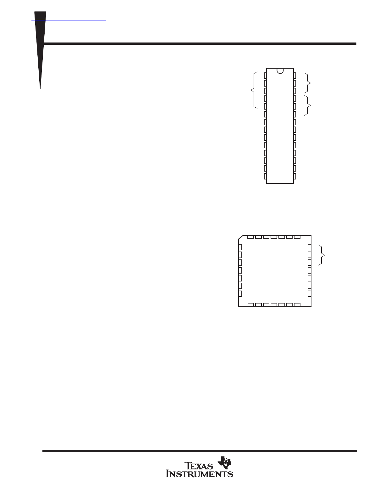
J PACKAGE
(TOP VIEW)
3
1
4
2
5
3
6
4
7
5
6
7
8
9
10
11
12
13
14
FK PACKAGE
(TOP VIEW)
INPUT 5
INPUT 4
INPUT 3
321
28 27 26
15 16 17 18
28
27
26
25
24
23
22
21
20
19
18
17
16
15
INPUT 1
INPUT 2
2
1
INPUTS
0
A
ADDRESS
B
C
ALE
–1
2
(MSB)
–2
2
–3
2
–4
2
2–8 (LSB)
REF–
–6
2
INPUT 0
25
A
B
24
C
23
ALE
22
–1
2
21
–2
2
20
–3
2
19
ADDRESS
(MSB)
The comparison and converting methods used
eliminate the possibility of missing codes,
nonmonotonicity, and the need for zero or
full-scale adjustment. Also featured are latched
GND
REF+
–6
2–72
REF–
(LSB)
–8
2
–4
2
3-state outputs from the SAR and latched inputs
to the multiplexer address decoder. The single 5-V
supply and low power requirements make the
ADC0808M especially useful for a wide variety of
applications. Ratiometric conversion is made
possible by access to the reference voltage input
terminals.
The ADC0808M is characterized for operation over the full military temperature range of –55°C to 125°C.
PRODUCTION DATA information is current as of publication date.
Products conform to specifications per the terms of Texas Instruments
standard warranty. Production processing does not necessarily include
testing of all parameters.
POST OFFICE BOX 655303 • DALLAS, TEXAS 75265
Copyright 1988, Texas Instruments Incorporated
1
ADC0808M
CMOS ANALOG-TO-DIGIT AL CONVERTER
WITH 8-CHANNEL MULTIPLEXER
SGLS005A – D2642, NOVEMBER 1986 – REVISED MAY 1988
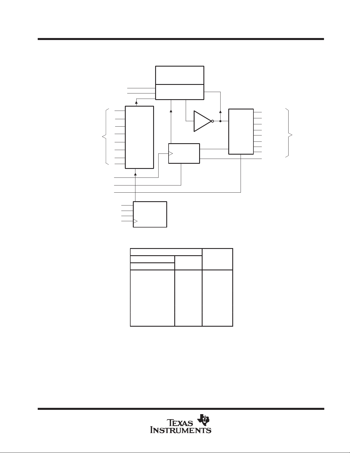
functional block diagram (positive logic)
Sample-and-Hold
Binary-Weighted
12
REF+
16
REF–
26
0
27
1
28
Analog
Inputs
2
3
4
5
6
7
1
2
3
4
5
Analog
Multiplexor
Capacitors
Switch
Matrix
Timing
and
Control
Threshold
Detector
Output
Latches
EN
17
14
15
8
18
19
20
21
7
–8
2
(LSB)
–7
2
–6
2
–5
2
–4
2
–3
2
–2
2
2–1(MSB)
EOC
Digital
Outputs
CLOCK
START
OEC
ALE
10
6
9
25
A
24
B
23
C
22
Address
Decoder
MULTIPLEXER FUNCTION TABLE
INPUTS
ADDRESS ADDRESS
C B A STROBE CHANNEL
L L L ↑ 0
L LH ↑ 1
LHL ↑ 2
LHH ↑
HLL ↑ 4
HLH ↑ 5
HHL ↑ 6
HHH ↑ 7
H = high level, L = low level
↑ = low-to-high transition
SELECTED
ANALOG
3
2
POST OFFICE BOX 655303 • DALLAS, TEXAS 75265
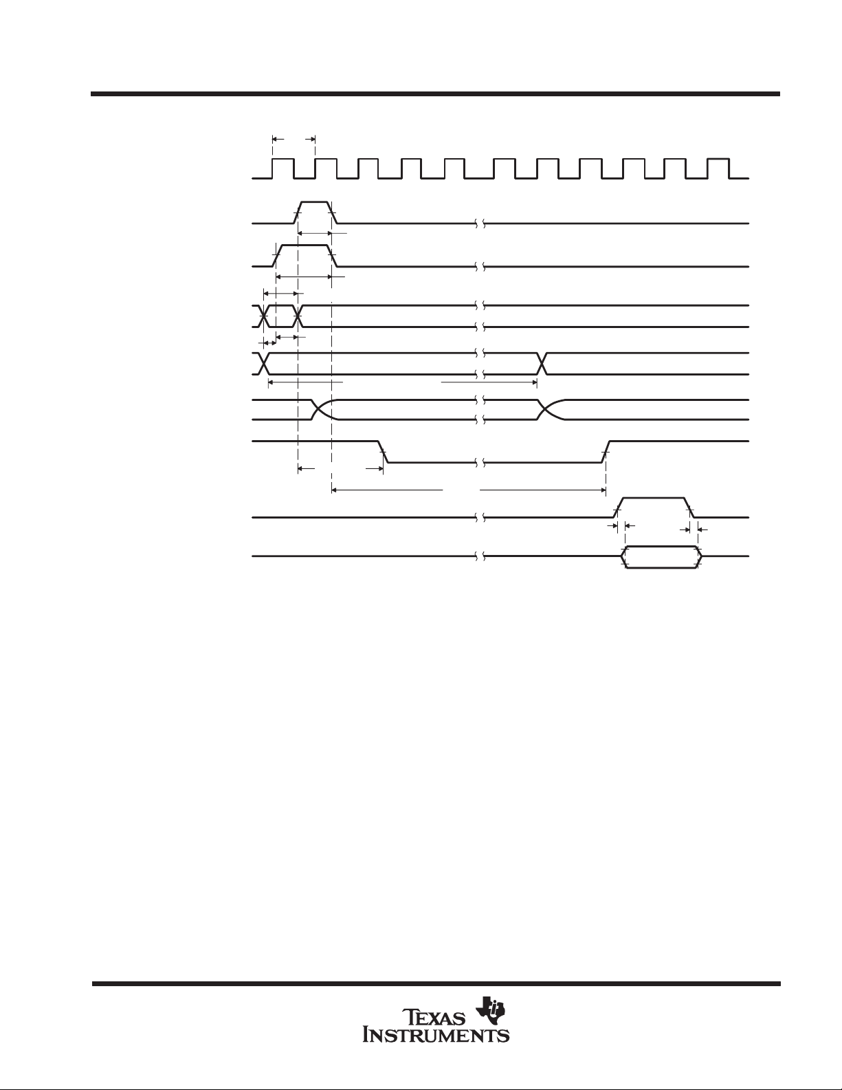
operating sequence
CLK
ADC0808M
CMOS ANALOG-TO-DIGIT AL CONVERTER
WITH 8-CHANNEL MULTIPLEXER
SGLS005A – D2642, NOVEMBER 1986 – REVISED MAY 1988
1/f
START
ALE
ADDRESS
INPUT
Multiplex Output
(Internal)
EOC
OEN
Latch Outputs
50%50%
t
w(S)
50%50%
t
w(ALC)
Address Stable
50%50%
t
t
su
h
Analog Value
Input Stable
Analog Value
50% 50%
t
d(EOC)
t
conv
Hi-Z State 10%
90%
50%50%
t
en
90%
10%
t
dis
POST OFFICE BOX 655303 • DALLAS, TEXAS 75265
3

ADC0808M
CMOS ANALOG-TO-DIGIT AL CONVERTER
WITH 8-CHANNEL MULTIPLEXER
SGLS005A – D2642, NOVEMBER 1986 – REVISED MAY 1988
absolute maximum ratings over operating free-air temperature range (unless otherwise noted)
Supply voltage, VCC (see Note 1) 6.5 V. . . . . . . . . . . . . . . . . . . . . . . . . . . . . . . . . . . . . . . . . . . . . . . . . . . . . . . . . . .
Input voltage range: Control inputs –0.3 V to 15 V. . . . . . . . . . . . . . . . . . . . . . . . . . . . . . . . . . . . . . . . . . . . . . . . . .
All other inputs –0.3 V to V
Operating free-air temperature range –55°C to 125°C. . . . . . . . . . . . . . . . . . . . . . . . . . . . . . . . . . . . . . . . . . . . . .
Storage temperature range –65°C to 150°C. . . . . . . . . . . . . . . . . . . . . . . . . . . . . . . . . . . . . . . . . . . . . . . . . . . . . . .
Case temperature for 60 seconds: FK package 260°C. . . . . . . . . . . . . . . . . . . . . . . . . . . . . . . . . . . . . . . . . . . . . .
Lead temperature 1,6 mm (1/16 inch) from case for 60 seconds: J package 300°C. . . . . . . . . . . . . . . . . . . . .
NOTE 1: All voltage values are with respect to network ground terminal.
recommended operating conditions
MIN NOM MAX UNIT
Supply voltage, V
Positive reference voltage, V
Negative reference voltage, V
Differential reference voltage, V
High-level input voltage, V
Low-level input voltage, V
Start pulse duration, t
Address load control pulse duration, t
Address setup time, t
Address hold time, t
Clock frequency, f
Operating free-air temperature, T
NOTE 2: Care must be taken that this rating is observed even during power-up.
CC
(see Note 2) V
ref +
ref –
ref +–Vref–
IH
IL
) 200 ns
w(S
w(ALC)
su
h
clock
A
4.5 5 6 V
CCVCC
VCC–1.5 V
200 ns
50 ns
50 ns
10 640 1280 kHz
–55 125 °C
0 –0.1 V
5 V
+ 0.3 V. . . . . . . . . . . . . . . . . . . . . . . . . . . . . . . . . . . . . . . . . .
CC
+0.1 V
1.5 V
4
POST OFFICE BOX 655303 • DALLAS, TEXAS 75265

ADC0808M
VOLLow-level output voltage
V
I
A
IonChannel on-state current (see Note 3)
A
nA
I
Channel off-state current
V
5 V
A
CMOS ANALOG-TO-DIGIT AL CONVERTER
WITH 8-CHANNEL MULTIPLEXER
SGLS005A – D2642, NOVEMBER 1986 – REVISED MAY 1988
electrical characteristics over recommended operating free-air temperature range, VCC = 4.5 V to
5.5 V (unless otherwise noted)
total device
PARAMETER TEST CONDITIONS MIN TYP†MAX UNIT
V
High-level output voltage IO = –360 µA VCC–0.4 V
OH
p
Off-state (high-impedance-state) VO = V
OZ
output current VO = 0 –3
IIControl input current at maiximum input voltage VI = 15 V 1 µA
I
Low-level control input current VI = 0 –1 µA
IL
I
Supply current f
CC
CiInput capacitance, control inputs TA = 25°C 10 pF
CoOutput capacitance, data outputs TA = 25°C 10 pF
Resistance from REF+ to REF – 1000 kΩ
analog multiplexer
PARAMETER TEST CONDITIONS MIN TYP†MAX UNIT
off
†
Typical values are at VCC = 5 V and TA = 25°C.
NOTE 3: Channel on-state current is primarily due to the bias current into or out of the threshold detector, and it varies directly with clock frequency .
Data outputs IO = 1.6 mA 0.45
End of conversion IO = 1.2 mA 0.45
CC
= 640 kHz 0.3 3 mA
clock
VI = VCC, f
VI = 0, f
VCC = 5 V, VI = 5 V 10 200
TA = 25°C VI = 0 –10 –200
=
CC
= 640 kHz 2
clock
= 640 kHz –2
clock
VI = 5 V 1
VI = 0 –1
3
µ
µ
µ
timing characteristics, VCC = V
PARAMETER TEST CONDITIONS MIN TYP MAX UNIT
f
clock
t
conv
t
enH
t
enL
t
dis
t
w(s)
t
w(ALE)
t
su
t
h
t
d(EOC)
NOTES: 4. Refer to the operating sequence diagram
Clock frequency 10 640 1280 kHz
Conversion time See Notes 4 and 5 and Figure 1 90 100 116 µs
Enable time, high See Figure 1 150 360 ns
Enable time, low See FIgure 1 90 25 ns
Output disable time See Figure 1 200 405 ns
Pulse duration, STAR T 200 ns
Pulse duration, ALE 200 ns
Setup time, ADDRESS 50 ns
Hold time, ADDRESS 50 ns
Delay time, EOC See Notes 4 and 6 and Figure 1 0 14.5 µs
5. For clock frequencies other than 640 kHz, t
6. For clock frequencies other than 640 kHz, t
ref+
= 5 V, V
= 0 V, TA = 25°C (unless otherwise noted)
ref–
is 57 clock cycles minimum and 74 clock cycles maximum.
conv
maximum is 8 clock cycles plus 2 µs.
d(EOC)
POST OFFICE BOX 655303 • DALLAS, TEXAS 75265
5

ADC0808M
Total unadjusted error (see Note 10)
LSB
CMOS ANALOG-TO-DIGIT AL CONVERTER
WITH 8-CHANNEL MULTIPLEXER
SGLS005A – D2642, NOVEMBER 1986 – REVISED MAY 1988
operating characteristics, T
= 25°C, VCC = V
A
ref+
= 5 V, V
ref–
= 0 V, f
= 640 kHz (unless
clock
otherwise noted)
PARAMETER TEST CONDITIONS MIN TYP†MAX UNIT
k
†
Typical values for all except supply voltage sensitivity are at VCC = 5 V, and all are at TA = 25°C.
NOTES: 7. Supply voltage sensitivity relates to the ability of an analog-to-digital converter to maintain accuracy as the supply voltage varies. The
Supply voltage sensitivity
SVS
Linearity error (see Note 8)
Zero error (see Note 9)
supply and V
8. Linearity error is the maximum deviation from a straight line through the end points of the A/D transfer characteristic.
9. Zero error is the difference between 00000000 and the converted output for zero input voltage; full-scale error is the differ ence between
11111111 and the converted output for full-scale input voltage.
10. Total unadjusted error is the maximum sum of linearity error, zero error, and full-scale error.
are varied together and the change in accuracy is measured with respect to full-scale.
ref+
VCC = V
TA = – 55°C to 125 °C, See Note 7
TA = 25°C
TA = –55°C to 125°C
= 4.5 V to 5.5 V,
ref +
±0.05 %/V
±0.25
±0.25
±0.25 ±0.5
±0.75
LSB
LSB
PARAMETER MEASUREMENT INFORMATION
V
CC
5 kΩ
Output
Test
Point
100 pF 11.7 kΩ
C
L
Figure 1. Test Circuit
6
POST OFFICE BOX 655303 • DALLAS, TEXAS 75265

ADC0808M
CMOS ANALOG-TO-DIGIT AL CONVERTER
WITH 8-CHANNEL MULTIPLEXER
SGLS005A – D2642, NOVEMBER 1986 – REVISED MAY 1988
PRINCIPLES OF OPERATION
The ADC0808M consists of an analog signal multiplexer, an 8-bit successive-approximation converter, and
related control and output circuitry.
multiplexer
The analog multiplexer selects 1 of 8 single-ended input channels as determined by the address decoder.
Address load control loads the address code into the decoder on a low-to-high transition. The output latch is
reset by the positive-going edge of the start pulse. Sampling also starts with the positive-going edge of the start
pulse and lasts for 32 clock periods. The conversion process may be interrupted by a new start pulse before
the end of 64 clock periods. The previous data will be lost if a new start of conversion occurs before the 64th
clock pulse. Continuous conversion may be accomplished by connecting the End-of-Conversion output to the
start input. If used in this mode an external pulse should be applied after power up to assure start up.
converter
The CMOS threshold detector in the successive-approximation conversion system determines each bit by
examining the charge on a series of binary-weighted capacitors (Figure 2). In the first phase of the conversion
process, the analog input is sampled by closing switch S
all the capacitors to the input voltage.
and all ST switches, and by simultaneously charging
C
In the next phase of the conversion process, all S
and S
T
switches are opened and the threshold detector
C
begins identifying bits by identifying the charge (voltage) on each capacitor relative to the reference voltage.
In the switching sequence, all eight capacitors are examined separately until all 8 bits are identified, and then
the charge-convert sequence is repeated. In the first step of the conversion phase, the threshold detector looks
at the first capacitor (weight = 128). Node 128 of this capacitor is switched to the reference voltage, and the
equivalent nodes of all the other capacitors on the ladder are switched to REF–. If the voltage at the summing
node is greater than the trip-point of the threshold detector (approximately one-half the V
voltage), a bit is
CC
placed in the output register, and the 128-weight capacitor is switched to REF–. If the voltage at the summing
node is less than the trip point of the threshold detector, this 128-weight capacitor remains connected to REF+
through the remainder of the capacitor-sampling (bit-counting) process. The process is repeated for the
64-weight capacitor, the 32-weight capacitor, and so forth down the line, until all bits are counted.
With each step of the capacitor-sampling process, the initial charge is redistributed among the capacitors.The
conversion process is successive approximation, but relies on charge redistribution rather than a
successive-approximation register (and reference DAC) to count and weigh the bits from MSB to LSB.
S
C
Threshold
Detctor
To
Output
Latches
128
Node 128
64
REF+
REF+
32
REF+
16
REF+
8
REF+
4
REF+
2
REF+
1
1
REF+
REF–
V
in
REF–
S
T
REF–
S
T
REF–
S
T
REF–
S
T
REF–
S
T
REF–
S
T
REF–
S
T
S
T
Figure 2. Simplified Model of the Successive-Approximation System
POST OFFICE BOX 655303 • DALLAS, TEXAS 75265
REF–
S
T
7

IMPORTANT NOTICE
T exas Instruments and its subsidiaries (TI) reserve the right to make changes to their products or to discontinue
any product or service without notice, and advise customers to obtain the latest version of relevant information
to verify, before placing orders, that information being relied on is current and complete. All products are sold
subject to the terms and conditions of sale supplied at the time of order acknowledgement, including those
pertaining to warranty, patent infringement, and limitation of liability.
TI warrants performance of its semiconductor products to the specifications applicable at the time of sale in
accordance with TI’s standard warranty. Testing and other quality control techniques are utilized to the extent
TI deems necessary to support this warranty . Specific testing of all parameters of each device is not necessarily
performed, except those mandated by government requirements.
CERT AIN APPLICATIONS USING SEMICONDUCTOR PRODUCTS MAY INVOLVE POTENTIAL RISKS OF
DEATH, PERSONAL INJURY, OR SEVERE PROPERTY OR ENVIRONMENTAL DAMAGE (“CRITICAL
APPLICATIONS”). TI SEMICONDUCTOR PRODUCTS ARE NOT DESIGNED, AUTHORIZED, OR
WARRANTED TO BE SUITABLE FOR USE IN LIFE-SUPPORT DEVICES OR SYSTEMS OR OTHER
CRITICAL APPLICA TIONS. INCLUSION OF TI PRODUCTS IN SUCH APPLICATIONS IS UNDERST OOD TO
BE FULLY AT THE CUSTOMER’S RISK.
In order to minimize risks associated with the customer’s applications, adequate design and operating
safeguards must be provided by the customer to minimize inherent or procedural hazards.
TI assumes no liability for applications assistance or customer product design. TI does not warrant or represent
that any license, either express or implied, is granted under any patent right, copyright, mask work right, or other
intellectual property right of TI covering or relating to any combination, machine, or process in which such
semiconductor products or services might be or are used. TI’s publication of information regarding any third
party’s products or services does not constitute TI’s approval, warranty or endorsement thereof.
Copyright 1998, Texas Instruments Incorporated
 Loading...