


D
Advanced LinCMOS Silicon-Gate
Technology
D
Easily interfaced to Microprocessors
D
On-Chip Data Latches
D
Monotonicity Over Entire A/D Conversion
Range
D
Segmented High-Order Bits Ensure
Low-Glitch Output
D
Designed to Be interchangeable With
Analog Devices AD7524, PMI PM-7524, and
Micro Power Systems MP7524
D
Fast Control Signaling for Digital Signal
Processor Applications Including Interface
With SMJ320
KEY PERFORMANCE SPECIFICATIONS
Resolution 8 Bits
Linearity error 1/2 LSB Max
Power dissipation at VDD = 5 V 5 mW Max
Settling time 100 ns Max
Propagation delay 80 ns Max
description
AD7524M
Advanced LinCMOS 8-BIT MULTIPLYING
DIGITAL-TO-ANALOG CONVERTER
SGLS028A – SEPTEMBER 1989 – REVISED MARCH 1995
J PACKAGE
(TOP VIEW)
NC
16
15
14
13
12
11
10
R
FB
9
R
REF
V
WR
CS
DB0
DB1
DB2
REF
18
17
16
15
14
FB
DD
V
DD
WR
NC
CS
DB0
GND
DB7
NC
DB6
DB5
OUT1
OUT2
GND
DB7
DB6
DB5
DB4
DB3
FK PACKAGE
(TOP VIEW)
OUT2
3 2 1 20 19
4
5
6
7
8
910111213
1
2
3
4
5
6
7
8
OUT1
The AD7524M is an Advanced LinCMOS 8-bit
digital-to-analog converter (DAC) designed for
easy interface to most popular microprocessors.
NC–No internal connection
DB4
DB3
NC
DB2
DB1
The AD7524M is an 8-bit multiplying DAC with input latches and with a load cycle similar to the write cycle of
a random access memory. Segmenting the high-order bits minimizes glitches during changes in the
most-significant bits, which produce the highest glitch impulse. The AD7524M provides accuracy to 1/2 LSB
without the need for thin-film resistors or laser trimming, while dissipating less than 5 mW typically.
Featuring operation from a 5-V to 15-V single supply , the AD7524M interfaces easily to most microprocessor
buses or output ports. Excellent multiplying (2 or 4 quadrant) makes the AD7524M an ideal choice for many
microprocessor-controlled gain-setting and signal-control applications.
The AD7524M is characterized for operation from –55°C to 125°C.
AVAILABLE OPTIONS
PACKAGE
T
A
–55°C to 125°C AD7524MFK AD7524MJ
CERAMIC CHIP
CARRIER
(FK)
CERAMIC DIP
(J)
Advanced LinCMOS is a trademark of Texas Instruments Incorporated.
PRODUCTION DATA information is current as of publication date.
Products conform to specifications per the terms of Texas Instruments
standard warranty. Production processing does not necessarily include
testing of all parameters.
POST OFFICE BOX 655303 • DALLAS, TEXAS 75265
Copyright 1995, Texas Instruments Incorporated
1

AD7524M
Advanced LinCMOS 8-BIT MULTIPLYING
DIGITAL-TO-ANALOG CONVERTER
SGLS028A – SEPTEMBER 1989 – REVISED MARCH 1995
functional block diagram
REF
CS
WR
operating sequence
15
12
13
2R
DB7
(MSB)
RRR
2R
Data Latches
DB6 DB5 DB0
Data Inputs
2R
(LSB)
tsu(CS)
2R
2R
16
R
FB
S-8S-3S-2S-1
11654
R
1
OUT1
2
OUT2
3
GND
th(CS)
CS
WR
DB0–DB7
10%
10%
tw(WR)
10%
tsu(D)
th(D)
2
POST OFFICE BOX 655303 • DALLAS, TEXAS 75265

UNIT
AD7524M
Advanced LinCMOS 8-BIT MULTIPLYING
DIGITAL-TO-ANALOG CONVERTER
SGLS028A – SEPTEMBER 1989 – REVISED MARCH 1995
absolute maximum ratings over operating free-air temperature range (unless otherwise noted)
Supply voltage range, V
Voltage between R
FB
Digital input voltage range, V
Reference voltage range, V
Peak digital input current, I
Operating free-air temperature range, T
Storage temperature range, T
Case temperature for 60 seconds, T
Lead temperature 1,6 mm (1/16 inch) from case for 60 seconds: J package 300°C. . . . . . . . . . . . . . . . . . . . .
†
Stresses beyond those listed under “absolute maximum ratings” may cause permanent damage to the device. These are stress ratings only, and
functional operation of the device at these or any other conditions beyond those indicated under “recommended operating conditions” is not
implied. Exposure to absolute-maximum-rated conditions for extended periods may affect device reliability.
–0.3 V to 17 V. . . . . . . . . . . . . . . . . . . . . . . . . . . . . . . . . . . . . . . . . . . . . . . . . . . . . . . . .
DD
and GND ±25 V. . . . . . . . . . . . . . . . . . . . . . . . . . . . . . . . . . . . . . . . . . . . . . . . . . . . . . . . . . . . .
–0.3 V to VDD+0.3 V. . . . . . . . . . . . . . . . . . . . . . . . . . . . . . . . . . . . . . . . . . . . . . . . .
I
±25 V. . . . . . . . . . . . . . . . . . . . . . . . . . . . . . . . . . . . . . . . . . . . . . . . . . . . . . . . . . . . . .
ref
10 µA. . . . . . . . . . . . . . . . . . . . . . . . . . . . . . . . . . . . . . . . . . . . . . . . . . . . . . . . . . . . . . . .
I
–65°C to 150°C. . . . . . . . . . . . . . . . . . . . . . . . . . . . . . . . . . . . . . . . . . . . . . . . . . .
stg
–55°C to 125°C. . . . . . . . . . . . . . . . . . . . . . . . . . . . . . . . . . . . . . . . . . .
A
: FK package 260°C. . . . . . . . . . . . . . . . . . . . . . . . . . . . . . . . . . . . . . . . . .
C
recommended operating conditions
VDD = 5 V VDD = 15 V
MIN NOM MAX MIN NOM MAX
Supply voltage, V
Reference voltage, V
High-level input voltage, V
Low-level input volage, V
CS setup time, t
CS hold time, t
Data bus input setup time, t
Data bus input hold time, t
Pulse duration, WR low, t
Operating free-air temperature, T
DD
ref
IH
IL
su(CS)
h(CS)
su(D)
h(D)
w(WR)
A
4.75 5 5.25 14.5 15 15.5 V
±10 ±10 V
2.4 13.5 V
0.8 1.5 V
40 40 ns
0 0 ns
25 25 ns
10 10 ns
40 40 ns
–55 125 –55 125 °C
†
POST OFFICE BOX 655303 • DALLAS, TEXAS 75265
3
AD7524M
PARAMETER
TEST CONDITIONS
UNIT
IIHHigh-level input current
V
V
A
IILLow-level input current
V
0
A
I
g
nA
Standb
DB0–DB7 at 0 V or V
A
k
yg y,
∆V
10%
DB0–DB7 at 0, WR
V
C
pF
DB0–DB7 at V
V
PARAMETER
TEST CONDITIONS
UNIT
Gain error
See Note 1
%FSR
Feedthrough at OUT1 or OUT2
ref
(),
%FSR
Advanced LinCMOS 8-BIT MULTIPLYING
DIGITAL-TO-ANALOG CONVERTER
SGLS028A – SEPTEMBER 1989 – REVISED MARCH 1995
electrical characteristics over recommended operating free-air temperature range, V
OUT1 and OUT2 at GND (unless otherwise noted)
VDD = 5 V VDD = 15 V
MIN TYP MAX MIN TYP MAX
Full-range 10 10
25°C 1 1
Full-range –10 –10
25°C –1 –1
Full-range ±400 ±200
Full-range ±400 ±200
Full-range 500 500
DD
25°C 100 100
Full-range 0.16 0.04 %/%
25°C 0.002 0.02 0.001 0.02 pF
30 30
120 120
120 120
30 30
5 20 5 20 kΩ
I
C
pkg
DD
p
p
Output leakage
current
Supply current
Supply voltage sensitivity,
SVS
∆gain/∆V
Input capacitance, DB0–DB7,
i
WR
Output
o
capacitance
Reference input impedance
(REF to GND)
DD
, CS
=
I
DD
=
I
DB0–DB7 at 0,
WR
OUT1
OUT2
Quiescent DB0–DB7 at VIHmin or VILmax 2 2 mA
y
OUT1
OUT2
OUT1
OUT2
and CS at 0 V
V
= ±10 V 25°C ±50 ±50
ref
DB0–DB7 at V
WR
and CS at 0
V
= ±10 V 25°C ±50 ±50
ref
DD
VI = 0 5 5 pF
=
DD,
and CS at 0
, WR and CS at 0
DD
= 10 V,
ref
µ
µ
µ
p
operating characteristics over recommended operating free-air temperature range, V
= 10 V,
ref
OUT1 and OUT2 at GND (unless otherwise noted)
VCC = 5 V VDD = 15 V
MIN MAX MIN MAX
Linearity error ±0.2 ±0.2 %FSR
Full range ±1.4 ±0.6
25°C ±1 ±0.5
Settling time (to 1/2 LSB) See Note 2 100 100 ns
Propagation delay from digital input to
90% of final analog output current
Temperature coefficient of gain TA = 25°C to t
NOTES: 1. Gain error is measured using the internal feedback resistor. Nominal Full Scale Range (FSR) = V
2. OUT1 load = 100 Ω, C
ext
See Note 2 80 80 ns
V
= ±10 V (100 kHz sinewave),
WR and CS at 0, DB0–DB7 at 0
or t
min
= 13 pF, WR
at 0 V, CS at 0 V, DB0–DB7 at 0 V to VDD or VDD to 0 V.
max
Full range 0.5 0.5
25°C 0.25 0.25
±0.004 ±0.001
– 1 LSB.
ref
%FSR/
°C
4
POST OFFICE BOX 655303 • DALLAS, TEXAS 75265

Advanced LinCMOS 8-BIT MULTIPLYING
DIGITAL-TO-ANALOG CONVERTER
SGLS028A – SEPTEMBER 1989 – REVISED MARCH 1995
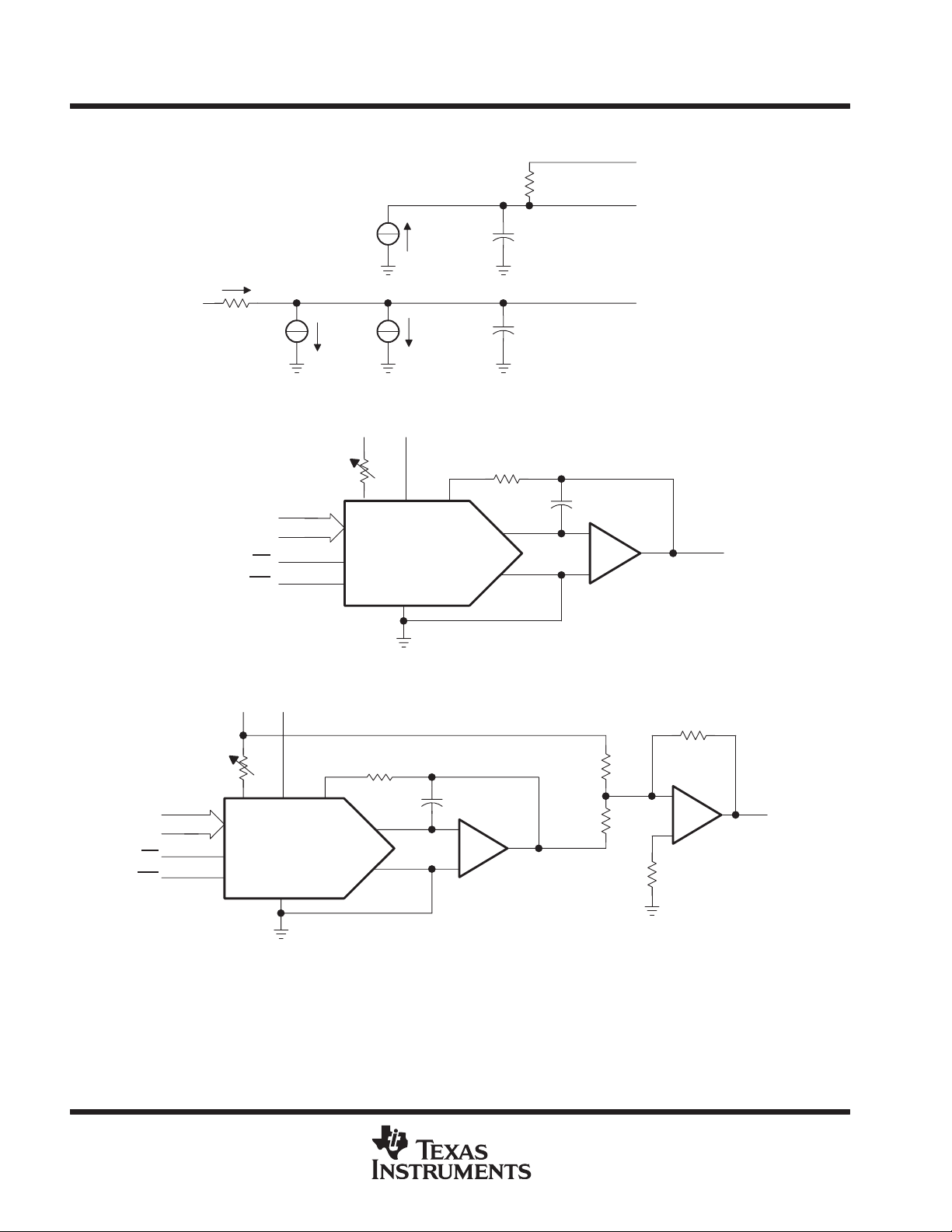
PRINCIPLES OF OPERATION
The AD7524M is an 8-bit multiplying D/A converter consisting of an inverted R-2R ladder, analog switches, and
data input latches. Binary weighted currents are switched between the OUT1 and OUT2 bus lines, thus
maintaining a constant current in each ladder leg independent of the switch state. The high-order bits are
decoded and these decoded bits, through a modification in the R-2R ladder, control three equally weighted
current sources. Most applications only require the addition of an external operational amplifier and a voltage
reference.
The equivalent circuit for all digital inputs low is seen in Figure 1. With all digital inputs low, the entire reference
current, I
termination resistor of the R-2R ladder, while the current source I
substrate. The capacitances appearing at OUT1 and OUT2 are dependent upon the digital input code. With all
digital inputs high, the off-state switch capacitance (30 pF maximum) appears at OUT2 and the on-state switch
capacitance (120 pF maximum) appears at OUT1. With all digital inputs low, the situation is reversed as shown
in Figure 1. Analysis of the circuit for all digital inputs high is similar to Figure 1; however, in this case, I
be switched to OUT1.
, is switched to OUT2. The current source 1/256 represents the constant current flowing through the
ref
represents leakage currents to the
Ikg
AD7524M
would
ref
Interfacing the AD7524M D/A converter to a microprocessor is accomplished via the data bus and the CS
WR
control signals. When CS and WR are both low, the AD7524M analog output responds to the data activity
on the DB0–DB7 data bus inputs. In this mode, the input latches are transparent and input data directly affects
the analog output. When either the CS signal or WR signal goes high, the data on the DB0–DB7 inputs are
latched until the CS
of the state of the WR
The AD7524M is capable of performing 2-quadrant or full 4-quadrant multiplication. Circuit configurations for
2-quadrant or 4-quadrant multiplication are shown in Figures 2 and 3. Input coding for unipolar and bipolar
operation are summarized in Tables 1 and 2, respectively.
and WR signals go low again. When CS is high, the data inputs are disabled regardless
signal.
and
POST OFFICE BOX 655303 • DALLAS, TEXAS 75265
5
AD7524M
Advanced LinCMOS 8-BIT MULTIPLYING
DIGITAL-TO-ANALOG CONVERTER
SGLS028A – SEPTEMBER 1989 – REVISED MARCH 1995
PRINCIPLES OF OPERATION
R
FB
R
OUT1
I
1kg
REF OUT2
1/256
I
1kg
30 pF
120 pF
Figure 1. AD7524M Equivalent Circuit With All Digital Inputs Low
V
V
ref
DD
DB0–DB7
CS
WR
RA = 2 kΩ
(see Note A)
R
FB
GND
OUT1
OUT2
R
B
C (see Note B)
–
+
Figure 2. Unipolar Operation (2-Quadrant Multiplication)
Output
V
V
ref
DD
DB0–DB7
CS
WR
RA = 2 kΩ
(see Note A)
GND
R
FB
OUT1
OUT2
R
B
Figure 3. Bipolar Operation (4-Quadrant Operation)
NOTES: A. RA and RB used only if gain adjustment is required.
B. C phase compensation (10 – 15 pF) is required when using high-speed amplifiers to prevent ringing or oscillation.
C (see Note B)
–
+
20 kΩ
10 kΩ
20 kΩ
–
+
5 kΩ
Output
6
POST OFFICE BOX 655303 • DALLAS, TEXAS 75265
microprocessor interfaces
PRINCIPLES OF OPERATION
Table 1. Unipolar Binary Code
DIGITAL INPUT
(see NOTE 3)
MSB LSB
11111111
10000001
10000000
01111111
00000001
00000000
NOTES: 3. LSB = 1/256 (V
Table 2. Bipolar (Offset Binary) Code
DIGITAL INPUT
(see NOTE 4)
MSB LSB
11111111
10000001
10000000
01111111
00000001
00000000
NOTES: 4. LSB = 1/128 (V
ref
ref
Advanced LinCMOS 8-BIT MULTIPLYING
DIGITAL-TO-ANALOG CONVERTER
SGLS028A – SEPTEMBER 1989 – REVISED MARCH 1995
ANALOG OUTPUT
–V
(255/256)
ref
–V
(129/256)
ref
–V
(128/256) = –V
ref
–V
(127/256)
ref
–V
(1/256)
ref
0
).
ANALOG OUTPUT
V
(127/128)
ref
V
(128)
ref
0
–V
(128)
ref
–V
(127/128)
ref
–V
ref
).
ref
/2
AD7524M
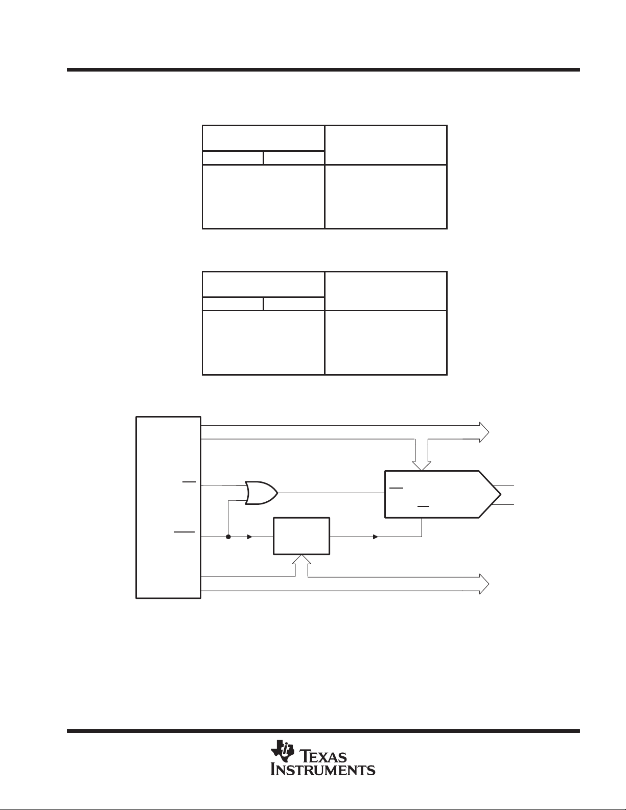
D0–D7
Z-80A
A0–A15
WR
IORQ
Data Bus
DB0–DB7
WR
Decode
Logic
Address Bus
Figure 4. AD7524M–Z-80A Interface
AD7524M
CS
OUT1
OUT2
POST OFFICE BOX 655303 • DALLAS, TEXAS 75265
7

AD7524M
Advanced LinCMOS 8-BIT MULTIPLYING
DIGITAL-TO-ANALOG CONVERTER
SGLS028A – SEPTEMBER 1989 – REVISED MARCH 1995
PRINCIPLES OF OPERATION
8051
D0–D7
6800
A0–A15
A8–A15
ALE
WR
Φ2
VMA
Data Bus
Decode
Logic
Address Bus
Figure 5. AD7524M–6800 Interface
Address Bus
Decode
Logic
8-Bit
Latch
DB0–DB7
WR
AD7524M
CS
WR
DB0–DB7
CS
AD7524M
OUT1
OUT2
OUT1
OUT2
AD0–AD7
Address/Data Bus
Figure 6. AD7524M–8051 Interface
8
POST OFFICE BOX 655303 • DALLAS, TEXAS 75265

IMPORTANT NOTICE
T exas Instruments and its subsidiaries (TI) reserve the right to make changes to their products or to discontinue
any product or service without notice, and advise customers to obtain the latest version of relevant information
to verify, before placing orders, that information being relied on is current and complete. All products are sold
subject to the terms and conditions of sale supplied at the time of order acknowledgement, including those
pertaining to warranty, patent infringement, and limitation of liability.
TI warrants performance of its semiconductor products to the specifications applicable at the time of sale in
accordance with TI’s standard warranty. Testing and other quality control techniques are utilized to the extent
TI deems necessary to support this warranty . Specific testing of all parameters of each device is not necessarily
performed, except those mandated by government requirements.
CERT AIN APPLICATIONS USING SEMICONDUCTOR PRODUCTS MAY INVOLVE POTENTIAL RISKS OF
DEATH, PERSONAL INJURY, OR SEVERE PROPERTY OR ENVIRONMENTAL DAMAGE (“CRITICAL
APPLICATIONS”). TI SEMICONDUCTOR PRODUCTS ARE NOT DESIGNED, AUTHORIZED, OR
WARRANTED TO BE SUITABLE FOR USE IN LIFE-SUPPORT DEVICES OR SYSTEMS OR OTHER
CRITICAL APPLICA TIONS. INCLUSION OF TI PRODUCTS IN SUCH APPLICATIONS IS UNDERST OOD TO
BE FULLY AT THE CUSTOMER’S RISK.
In order to minimize risks associated with the customer’s applications, adequate design and operating
safeguards must be provided by the customer to minimize inherent or procedural hazards.
TI assumes no liability for applications assistance or customer product design. TI does not warrant or represent
that any license, either express or implied, is granted under any patent right, copyright, mask work right, or other
intellectual property right of TI covering or relating to any combination, machine, or process in which such
semiconductor products or services might be or are used. TI’s publication of information regarding any third
party’s products or services does not constitute TI’s approval, warranty or endorsement thereof.
Copyright 1998, Texas Instruments Incorporated
 Loading...