


A7805C
A7808C
10
0°C to 125°C
A7812C
A7815C
24
查询uA7800供应商
D
3-Terminal Regulators
D
Output Current up to 1.5 A
D
Internal Thermal-Overload Protection
KC (TO-220) PACKAGE
(TOP VIEW)
µA7800 SERIES
POSITIVE-VOLTAGE REGULATORS
SLVS056J – MAY 1976 – REVISED MA Y 2003
D
High Power-Dissipation Capability
D
Internal Short-Circuit Current Limiting
D
Output Transistor Safe-Area Compensation
KTE PACKAGE
(TOP VIEW)
COMMON
KCS (TO-220) PACKAGE
(TOP VIEW)
OUTPUT
COMMON
INPUT
COMMON
OUTPUT
COMMON
INPUT
OUTPUT
COMMON
INPUT
COMMON
description/ordering information
This series of fixed-voltage integrated-circuit voltage regulators is designed for a wide range of applications.
These applications include on-card regulation for elimination of noise and distribution problems associated with
single-point regulation. Each of these regulators can deliver up to 1.5 A of output current. The internal
current-limiting and thermal-shutdown features of these regulators essentially make them immune to overload.
In addition to use as fixed-voltage regulators, these devices can be used with external components to obtain
adjustable output voltages and currents, and also can be used as the power-pass element in precision
regulators.
ORDERING INFORMATION
V
T
J
†
Package drawings, standard packing quantities, thermal data, symbolization, and PCB design guidelines are available at
www.ti.com/sc/package.
O(NOM)
(V)
5
8
12
15
PACKAGE
POWER-FLEX (KTE) Reel of 2000 µA7805CKTER µA7805C
TO-220 (KC) Tube of 50 µA7805CKC
TO-220, short shoulder (KCS) Tube of 20 µA7805CKCS
POWER-FLEX (KTE) Reel of 2000 µA7808CKTER µA7808C
TO-220 (KC) Tube of 50 µA7808CKC
TO-220, short shoulder (KCS) Tube of 20 µA7808CKCS
POWER-FLEX (KTE) Reel of 2000 µA7810CKTER µA7810C
TO-220 (KC) Tube of 50 µA7810CKC µA7810C
POWER-FLEX (KTE) Reel of 2000 µA7812CKTER µA7812C
TO-220 (KC) Tube of 50 µA7812CKC
TO-220, short shoulder (KCS) Tube of 20 µA7812CKCS
POWER-FLEX (KTE) Reel of 2000 µA7815CKTER µA7815C
TO-220 (KC) Tube of 50 µA7815CKC
TO-220, short shoulder (KCS) Tube of 20 µA7815CKCS
POWER-FLEX (KTE) Reel of 2000 µA7824CKTER µA7824C
TO-220 (KC) Tube of 50 µA7824CKC µA7824C
†
ORDERABLE
PART NUMBER
TOP-SIDE
MARKING
µ
µ
µ
µ
Please be aware that an important notice concerning availability, standard warranty, and use in critical applications of
Texas Instruments semiconductor products and disclaimers thereto appears at the end of this data sheet.
PRODUCTION DATA information is current as of publication date.
Products conform to specifications per the terms of Texas Instruments
standard warranty. Production processing does not necessarily include
testing of all parameters.
POST OFFICE BOX 655303 • DALLAS, TEXAS 75265
Copyright 2003, Texas Instruments Incorporated
1
µA7800 SERIES
POSITIVE-VOLTAGE REGULATORS
SLVS056J – MAY 1976 – REVISED MAY 2003
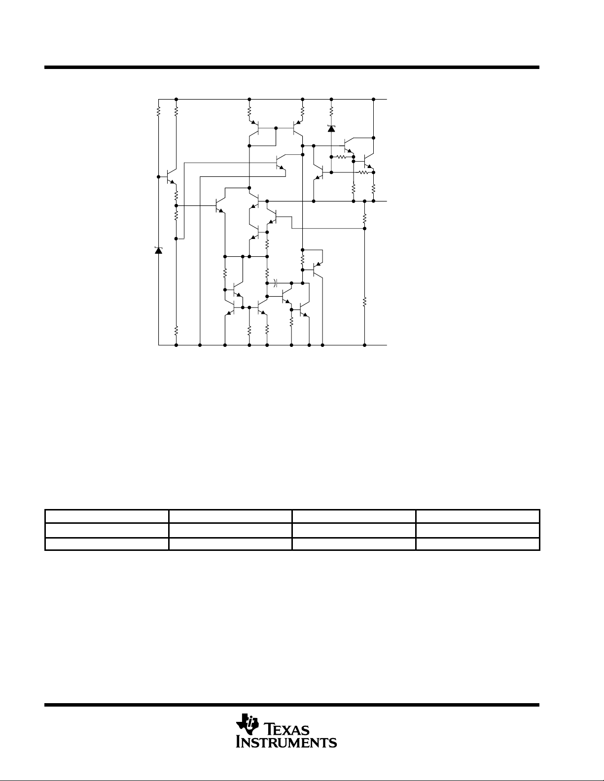
schematic
INPUT
OUTPUT
COMMON
absolute maximum ratings over virtual junction temperature range (unless otherwise noted)
Input voltage, V
: µA7824C 40 V. . . . . . . . . . . . . . . . . . . . . . . . . . . . . . . . . . . . . . . . . . . . . . . . . . . . . . . . . . . . . . . . .
I
†
All others 35 V. . . . . . . . . . . . . . . . . . . . . . . . . . . . . . . . . . . . . . . . . . . . . . . . . . . . . . . . . . . . . . . . .
Operating virtual junction temperature, T
150°C. . . . . . . . . . . . . . . . . . . . . . . . . . . . . . . . . . . . . . . . . . . . . . . . . . .
J
Lead temperature 1,6 mm (1/16 inch) from case for 10 seconds 260°C. . . . . . . . . . . . . . . . . . . . . . . . . . . . . .
Storage temperature range, T
†
Stresses beyond those listed under “absolute maximum ratings” may cause permanent damage to the device. These are stress ratings only, and
functional operation of the device at these or any other conditions beyond those indicated under “recommended operating conditions” is not
implied. Exposure to absolute-maximum-rated conditions for extended periods may affect device reliability.
stg
–65°C to 150°C. . . . . . . . . . . . . . . . . . . . . . . . . . . . . . . . . . . . . . . . . . . . . . . . . . . .
package thermal data (see Note 1)
PACKAGE BOARD θ
POWER-FLEX (KTE) High K, JESD 51-5 3°C/W 23°C/W
TO-220 (KC/KCS) High K, JESD 51-5 3°C/W 19°C/W
NOTE 1: Maximum power dissipation is a function of TJ(max), θJA, and TA. The maximum allowable power dissipation at any allowable ambient
temperature is PD = (TJ(max) – TA)/θJA. Operating at the absolute maximum TJ of 150°C can affect reliability.
JC
θ
JA
2
POST OFFICE BOX 655303 • DALLAS, TEXAS 75265
µA7800 SERIES
VIInput voltage
V
PARAMETER
TEST CONDITIONS
T
†
UNIT
Output voltage
O
,
I
,
V
Input voltage regulation
25°C
mV
Output voltage regulation
25°C
mV
Bias current change
0°C to 125°C
mA
POSITIVE-VOLTAGE REGULATORS
SLVS056J – MAY 1976 – REVISED MAY 2003
recommended operating conditions
MIN MAX UNIT
µA7805C 7 25
µA7808C 10.5 25
p
I
Output current 1.5 A
O
T
Operating virtual junction temperature µA7800C series 0 125 °C
J
electrical characteristics at specified virtual junction temperature, VI = 10 V, IO = 500 mA (unless
otherwise noted)
I
p
p
Ripple rejection VI = 8 V to 18 V, f = 120 Hz 0°C to 125°C 62 78 dB
p
Output resistance f = 1 kHz 0°C to 125°C 0.017 Ω
Temperature coefficient of output voltage IO = 5 mA 0°C to 125°C –1.1 mV/°C
Output noise voltage f = 10 Hz to 100 kHz 25°C 40 µV
Dropout voltage IO = 1 A 25°C 2 V
Bias current 25°C 4.2 8 mA
Short-circuit output current 25°C 750 mA
Peak output current 25°C 2.2 A
†
Pulse-testing techniques maintain the junction temperature as close to the ambient temperature as possible. Thermal effects must be taken into
account separately . All characteristics are measured with a 0.33-µF capacitor across the input and a 0.1-µF capacitor across the output.
= 5 mA to 1 A, V
PD ≤ 15 W
VI = 7 V to 25 V
VI = 8 V to 12 V
IO = 5 mA to 1.5 A
IO = 250 mA to 750 mA
VI = 7 V to 25 V
IO = 5 mA to 1 A
= 7 V to 20 V,
µA7810C 12.5 28
µA7812C 14.5 30
µA7815C 17.5 30
µA7824C 27 38
J
25°C 4.8 5 5.2
0°C to 125°C 4.75 5.25
µA7805C
MIN TYP MAX
3 100
1 50
15 100
5 50
1.3
0.5
POST OFFICE BOX 655303 • DALLAS, TEXAS 75265
3
µA7800 SERIES
PARAMETER
TEST CONDITIONS
T
†
UNIT
Output voltage
O
,
I
,
V
Input voltage regulation
25°C
mV
Output voltage regulation
25°C
mV
Bias current change
0°C to 125°C
mA
PARAMETER
TEST CONDITIONS
T
†
UNIT
Output voltage
O
,
I
,
V
Input voltage regulation
25°C
mV
Output voltage regulation
25°C
mV
Bias current change
0°C to 125°C
mA
POSITIVE-VOLTAGE REGULATORS
SLVS056J – MAY 1976 – REVISED MAY 2003
electrical characteristics at specified virtual junction temperature, VI = 14 V, IO = 500 mA (unless
otherwise noted)
J
I
p
p
Ripple rejection VI = 11.5 V to 21.5 V, f = 120 Hz 0°C to 125°C 55 72 dB
p
Output resistance f = 1 kHz 0°C to 125°C 0.016 Ω
Temperature coefficient of output voltage IO = 5 mA 0°C to 125°C –0.8 mV/°C
Output noise voltage f = 10 Hz to 100 kHz 25°C 52 µV
Dropout voltage IO = 1 A 25°C 2 V
Bias current 25°C 4.3 8 mA
Short-circuit output current 25°C 450 mA
Peak output current 25°C 2.2 A
†
Pulse-testing techniques maintain the junction temperature as close to the ambient temperature as possible. Thermal effects must be taken into
account separately . All characteristics are measured with a 0.33-µF capacitor across the input and a 0.1-µF capacitor across the output.
= 5 mA to 1 A, V
PD ≤ 15 W
VI = 10.5 V to 25 V
VI = 11 V to 17 V
IO = 5 mA to 1.5 A
IO = 250 mA to 750 mA
VI = 10.5 V to 25 V
IO = 5 mA to 1 A
= 10.5 V to 23 V,
25°C 7.7 8 8.3
0°C to 125°C 7.6 8.4
°
µA7808C
MIN TYP MAX
6 160
2 80
12 160
4 80
1
0.5
electrical characteristics at specified virtual junction temperature, VI = 17 V, IO = 500 mA (unless
otherwise noted)
J
I
p
p
Ripple rejection VI = 13 V to 23 V, f = 120 Hz 0°C to 125°C 55 71 dB
p
Output resistance f = 1 kHz 0°C to 125°C 0.018 Ω
Temperature coefficient of output voltage IO = 5 mA 0°C to 125°C –1 mV/°C
Output noise voltage f = 10 Hz to 100 kHz 25°C 70 µV
Dropout voltage IO = 1 A 25°C 2 V
Bias current 25°C 4.3 8 mA
Short-circuit output current 25°C 400 mA
Peak output current 25°C 2.2 A
†
Pulse-testing techniques maintain the junction temperature as close to the ambient temperature as possible. Thermal effects must be taken into
account separately . All characteristics are measured with a 0.33-µF capacitor across the input and a 0.1-µF capacitor across the output.
= 5 mA to 1 A, V
PD ≤ 15 W
VI = 12.5 V to 28 V
VI = 14 V to 20 V
IO = 5 mA to 1.5 A
IO = 250 mA to 750 mA
VI = 12.5 V to 28 V
IO = 5 mA to 1 A
= 12.5 V to 25 V,
25°C 9.6 10 10.4
0°C to 125°C 9.5 10 10.5
µA7810C
MIN TYP MAX
7 200
2 100
12 200
4 100
1
0.5
4
POST OFFICE BOX 655303 • DALLAS, TEXAS 75265
µA7800 SERIES
PARAMETER
TEST CONDITIONS
T
†
UNIT
Output voltage
O
,
I
,
V
Input voltage regulation
25°C
mV
Output voltage regulation
25°C
mV
Bias current change
0°C to 125°C
mA
PARAMETER
TEST CONDITIONS
T
†
UNIT
Output voltage
O
,
I
,
V
Input voltage regulation
25°C
mV
Output voltage regulation
25°C
mV
Bias current change
0°C to 125°C
mA
POSITIVE-VOLTAGE REGULATORS
SLVS056J – MAY 1976 – REVISED MAY 2003
electrical characteristics at specified virtual junction temperature, VI = 19 V, IO = 500 mA (unless
otherwise noted)
J
I
p
p
Ripple rejection VI = 15 V to 25 V, f = 120 Hz 0°C to 125°C 55 71 dB
p
Output resistance f = 1 kHz 0°C to 125°C 0.018 Ω
Temperature coefficient of output voltage IO = 5 mA 0°C to 125°C –1 mV/°C
Output noise voltage f = 10 Hz to 100 kHz 25°C 75 µV
Dropout voltage IO = 1 A 25°C 2 V
Bias current 25°C 4.3 8 mA
Short-circuit output current 25°C 350 mA
Peak output current 25°C 2.2 A
†
Pulse-testing techniques maintain the junction temperature as close to the ambient temperature as possible. Thermal effects must be taken into
account separately . All characteristics are measured with a 0.33-µF capacitor across the input and a 0.1-µF capacitor across the output.
= 5 mA to 1 A, V
PD ≤ 15 W
VI = 14.5 V to 30 V
VI = 16 V to 22 V
IO = 5 mA to 1.5 A
IO = 250 mA to 750 mA
VI = 14.5 V to 30 V
IO = 5 mA to 1 A
= 14.5 V to 27 V,
25°C 11.5 12 12.5
0°C to 125°C 11.4 12.6
°
µA7812C
MIN TYP MAX
10 240
3 120
12 240
4 120
1
0.5
electrical characteristics at specified virtual junction temperature, VI = 23 V, IO = 500 mA (unless
otherwise noted)
J
I
p
p
Ripple rejection VI = 18.5 V to 28.5 V, f = 120 Hz 0°C to 125°C 54 70 dB
p
Output resistance f = 1 kHz 0°C to 125°C 0.019 Ω
Temperature coefficient of output voltage IO = 5 mA 0°C to 125°C –1 mV/°C
Output noise voltage f = 10 Hz to 100 kHz 25°C 90 µV
Dropout voltage IO = 1 A 25°C 2 V
Bias current 25°C 4.4 8 mA
Short-circuit output current 25°C 230 mA
Peak output current 25°C 2.1 A
†
Pulse-testing techniques maintain the junction temperature as close to the ambient temperature as possible. Thermal effects must be taken into
account separately . All characteristics are measured with a 0.33-µF capacitor across the input and a 0.1-µF capacitor across the output.
= 5 mA to 1 A, V
PD ≤ 15 W
VI = 17.5 V to 30 V
VI = 20 V to 26 V
IO = 5 mA to 1.5 A
IO = 250 mA to 750 mA
VI = 17.5 V to 30 V
IO = 5 mA to 1 A
= 17.5 V to 30 V,
25°C 14.4 15 15.6
0°C to 125°C 14.25 15.75
µA7815C
MIN TYP MAX
11 300
3 150
12 300
4 150
1
0.5
POST OFFICE BOX 655303 • DALLAS, TEXAS 75265
5

µA7800 SERIES
PARAMETER
TEST CONDITIONS
T
†
UNIT
Output voltage
O
,
I
,
V
Input voltage regulation
25°C
mV
Output voltage regulation
25°C
mV
Bias current change
0°C to 125°C
mA
POSITIVE-VOLTAGE REGULATORS
SLVS056J – MAY 1976 – REVISED MAY 2003
electrical characteristics at specified virtual junction temperature, VI = 33 V, IO = 500 mA (unless
otherwise noted)
J
I
p
p
Ripple rejection VI = 28 V to 38 V, f = 120 Hz 0°C to 125°C 50 66 dB
p
Output resistance f = 1 kHz 0°C to 125°C 0.028 Ω
Temperature coefficient of output voltage IO = 5 mA 0°C to 125°C –1.5 mV/°C
Output noise voltage f = 10 Hz to 100 kHz 25°C 170 µV
Dropout voltage IO = 1 A 25°C 2 V
Bias current 25°C 4.6 8 mA
Short-circuit output current 25°C 150 mA
Peak output current 25°C 2.1 A
†
Pulse-testing techniques maintain the junction temperature as close to the ambient temperature as possible. Thermal effects must be taken into
account separately . All characteristics are measured with a 0.33-µF capacitor across the input and a 0.1-µF capacitor across the output.
= 5 mA to 1 A, V
PD ≤ 15 W
VI = 27 V to 38 V
VI = 30 V to 36 V
IO = 5 mA to 1.5 A
IO = 250 mA to 750 mA
VI = 27 V to 38 V
IO = 5 mA to 1 A
= 27 V to 38 V,
25°C 23 24 25
0°C to 125°C 22.8 25.2
°
µA7824C
MIN TYP MAX
18 480
6 240
12 480
4 240
1
0.5
6
POST OFFICE BOX 655303 • DALLAS, TEXAS 75265

POSITIVE-VOLTAGE REGULATORS
APPLICATION INFORMATION
µA7800 SERIES
SLVS056J – MAY 1976 – REVISED MAY 2003
+V
µA78xx
+V
O
0.1 µF0.33 µF
Figure 1. Fixed-Output Regulator
COM
OUTIN
G
I
L
–V
O
+
V
I
–
µA78xx
Figure 2. Positive Regulator in Negative Configuration (VI Must Float)
Input Output
µA78xx
I
O
0.33 µF
R1
0.1 µF
R2
NOTE A: The following formula is used when Vxx is the nominal output voltage (output to common) of the fixed regulator:
V
xx
Vxx)
ǒ
V
+
O
R1
Ǔ
)
I
R2
Q
Figure 3. Adjustable-Output Regulator
Input
0.33 µF
IO = (VO/R1) + IO Bias Current
µA78xx
V
O(Reg)
R1
Output
I
O
Figure 4. Current Regulator
POST OFFICE BOX 655303 • DALLAS, TEXAS 75265
7

µA7800 SERIES
POSITIVE-VOLTAGE REGULATORS
SLVS056J – MAY 1976 – REVISED MAY 2003
APPLICATION INFORMATION
1N4001
20-V Input
0.33 µF
–20-V Input
2 µF
µA7815C
µA7915C
1N4001
1 µF
0.1 µF
0.1 µF
VO = 15 V
1N4001
1N4001
VO = –15 V
Figure 5. Regulated Dual Supply
operation with a load common to a voltage of opposite polarity
In many cases, a regulator powers a load that is not connected to ground but, instead, is connected to a voltage
source of opposite polarity (e.g., operational amplifiers, level-shifting circuits, etc.). In these cases, a clamp
diode should be connected to the regulator output as shown in Figure 6. This protects the regulator from output
polarity reversals during startup and short-circuit operation.
+V
I
µA78xx
1N4001
or
Equivalent
+V
O
–V
O
Figure 6. Output Polarity-Reversal-Protection Circuit
reverse-bias protection
Occasionally , the input voltage to the regulator can collapse faster than the output voltage. This can occur, for
example, when the input supply is crowbarred during an output overvoltage condition. If the output voltage is
greater than approximately 7 V , the emitter-base junction of the series-pass element (internal or external) could
break down and be damaged. To prevent this, a diode shunt can be used as shown in Figure 7.
V
I
µA78xx
Figure 7. Reverse-Bias-Protection Circuit
+V
O
8
POST OFFICE BOX 655303 • DALLAS, TEXAS 75265

PACKAGE OPTION ADDENDUM
www.ti.com
1-Mar-2005
PACKAGING INFORMATION
Orderable Device Status
(1)
Package
Type
Package
Drawing
Pins Package
Qty
Eco Plan
UA7805CKC ACTIVE TO-220 KC 3 50 None Call TI Level-1-220C-UNLIM
UA7805CKCS ACTIVE TO-220 KCS 3 50 None Call TI Level-NC-NC-NC
UA7805CKTER ACTIVE PFM KTE 3 2000 None Call TI Level-1-220C-UNLIM
UA7805QKC OBSOLETE TO-220 KC 3 None Call TI Call TI
UA7805QKTE OBSOLETE PFM KTE 3 None Call TI Call TI
UA7806CKC OBSOLETE TO-220 KC 3 None Call TI Call TI
UA7806CKTER OBSOLETE PFM KTE 3 None Call TI Call TI
UA7806QKTE OBSOLETE PFM KTE 3 None Call TI Call TI
UA7806QKTER OBSOLETE PFM KTE 3 None Call TI Call TI
UA7808CKC ACTIVE TO-220 KC 3 50 None Call TI Level-1-220C-UNLIM
UA7808CKCS ACTIVE TO-220 KCS 3 50 None Call TI Level-NC-NC-NC
UA7808CKTER ACTIVE PFM KTE 3 2000 None Call TI Level-1-220C-UNLIM
UA7808QKTE OBSOLETE PFM KTE 3 None Call TI Call TI
UA7810CKC ACTIVE TO-220 KC 3 50 None Call TI Level-1-220C-UNLIM
UA7810CKCS ACTIVE TO-220 KCS 3 50 None CU Level-NC-NC-NC
UA7810CKTER ACTIVE PFM KTE 3 2000 None Call TI Level-1-220C-UNLIM
UA7810QKTE OBSOLETE PFM KTE 3 None Call TI Call TI
UA7812CKC ACTIVE TO-220 KC 3 50 None Call TI Level-1-220C-UNLIM
UA7812CKCS ACTIVE TO-220 KCS 3 50 None Call TI Level-NC-NC-NC
UA7812CKTER ACTIVE PFM KTE 3 2000 None Call TI Level-1-220C-UNLIM
UA7812QKTE OBSOLETE PFM KTE 3 None Call TI Call TI
UA7815CKC ACTIVE TO-220 KC 3 50 None Call TI Level-1-220C-UNLIM
UA7815CKCS ACTIVE TO-220 KCS 3 50 None Call TI Level-NC-NC-NC
UA7815CKTER ACTIVE PFM KTE 3 2000 None Call TI Level-1-220C-UNLIM
UA7815QKTE OBSOLETE PFM KTE 3 None Call TI Call TI
UA7818CKC OBSOLETE TO-220 KC 3 None Call TI Call TI
UA7818CKTER OBSOLETE PFM KTE 3 None Call TI Call TI
UA7824CKC ACTIVE TO-220 KC 3 50 None Call TI Level-1-220C-UNLIM
UA7824CKCS ACTIVE TO-220 KCS 3 50 None CU Level-NC-NC-NC
UA7824CKTER ACTIVE PFM KTE 3 2000 None Call TI Level-1-220C-UNLIM
UA7885CKC OBSOLETE TO-220 KC 3 None Call TI Call TI
UA7885CKTER OBSOLETE PFM KTE 3 None Call TI Call TI
UA7885QKTE OBSOLETE PFM KTE 3 None Call TI Call TI
(1)
The marketing status values are defined as follows:
ACTIVE: Product device recommended for new designs.
LIFEBUY: TI has announced that the device will be discontinued, and a lifetime-buy period is in effect.
NRND: Not recommended for new designs. Device is in production to support existing customers, but TI does not recommend using this part in
a new design.
PREVIEW: Device has been announced but is not in production. Samples may or may not be available.
OBSOLETE: TI has discontinued the production of the device.
(2)
Lead/Ball Finish MSL Peak Temp
(3)
(2)
Eco Plan - May not be currently available - please check http://www.ti.com/productcontent for the latest availability information and additional
product content details.
None: Not yet available Lead (Pb-Free).
Addendum-Page 1

PACKAGE OPTION ADDENDUM
www.ti.com
Pb-Free (RoHS): TI's terms "Lead-Free" or "Pb-Free" mean semiconductor products that are compatible with the current RoHS requirements
for all 6 substances, including the requirement that lead not exceed 0.1% by weight in homogeneous materials. Where designed to be soldered
at high temperatures, TI Pb-Free products are suitable for use in specified lead-free processes.
Green (RoHS & no Sb/Br): TI defines "Green" to mean "Pb-Free" and in addition, uses package materials that do not contain halogens,
including bromine (Br) or antimony (Sb) above 0.1% of total product weight.
(3)
MSL, Peak Temp. -- The Moisture Sensitivity Level rating according to the JEDECindustry standard classifications, and peak solder
temperature.
Important Information and Disclaimer:The information provided on this page represents TI's knowledge and belief as of the date that it is
provided. TI bases its knowledge and belief on information provided by third parties, and makes no representation or warranty as to the
accuracy of such information. Efforts are underway to better integrate information from third parties. TI has taken and continues to take
reasonable steps to provide representative and accurate information but may not have conducted destructive testing or chemical analysis on
incoming materials and chemicals. TI and TI suppliers consider certain information to be proprietary, and thus CAS numbers and other limited
information may not be available for release.
In no event shall TI's liability arising out of such information exceed the total purchase price of the TI part(s) at issue in this document sold by TI
to Customer on an annual basis.
1-Mar-2005
Addendum-Page 2

MECHANICAL DATA
MPFM001E – OCTOBER 1994 – REVISED JANUARY 2001
KTE (R-PSFM-G3) PowerFLEX PLASTIC FLANGE-MOUNT
0.420 (10,67)
0.410 (10,41)
0.295 (7,49)
NOM
0.100 (2,54)
0.200 (5,08)
1
0.375 (9,52)
0.365 (9,27)
0.360 (9,14)
0.350 (8,89)
0.220 (5,59)
NOM
3
0.025 (0,63)
0.031 (0,79)
0.320 (8,13)
0.310 (7,87)
0.010 (0,25)
0.360 (9,14)
0.350 (8,89)
M
0.080 (2,03)
0.070 (1,78)
0.050 (1,27)
0.040 (1,02)
0.010 (0,25) NOM
Thermal Tab
(See Note C)
Seating Plane
0.004 (0,10)
0.005 (0,13)
0.001 (0,03)
NOTES: A. All linear dimensions are in inches (millimeters).
B. This drawing is subject to change without notice.
C. The center lead is in electrical contact with the thermal tab.
D. Dimensions do not include mold protrusions, not to exceed 0.006 (0,15).
E. Falls within JEDEC MO-169
PowerFLEX is a trademark of Texas Instruments.
0.010 (0,25)
NOM
0.041 (1,04)
0.031 (0,79)
Gage Plane
3°–6°
0.010 (0,25)
4073375/F 12/00
POST OFFICE BOX 655303 • DALLAS, TEXAS 75265
1


IMPORTANT NOTICE
Texas Instruments Incorporated and its subsidiaries (TI) reserve the right to make corrections, modifications,
enhancements, improvements, and other changes to its products and services at any time and to discontinue
any product or service without notice. Customers should obtain the latest relevant information before placing
orders and should verify that such information is current and complete. All products are sold subject to TI’s terms
and conditions of sale supplied at the time of order acknowledgment.
TI warrants performance of its hardware products to the specifications applicable at the time of sale in
accordance with TI’s standard warranty. Testing and other quality control techniques are used to the extent TI
deems necessary to support this warranty . Except where mandated by government requirements, testing of all
parameters of each product is not necessarily performed.
TI assumes no liability for applications assistance or customer product design. Customers are responsible for
their products and applications using TI components. To minimize the risks associated with customer products
and applications, customers should provide adequate design and operating safeguards.
TI does not warrant or represent that any license, either express or implied, is granted under any TI patent right,
copyright, mask work right, or other TI intellectual property right relating to any combination, machine, or process
in which TI products or services are used. Information published by TI regarding third-party products or services
does not constitute a license from TI to use such products or services or a warranty or endorsement thereof.
Use of such information may require a license from a third party under the patents or other intellectual property
of the third party, or a license from TI under the patents or other intellectual property of TI.
Reproduction of information in TI data books or data sheets is permissible only if reproduction is without
alteration and is accompanied by all associated warranties, conditions, limitations, and notices. Reproduction
of this information with alteration is an unfair and deceptive business practice. TI is not responsible or liable for
such altered documentation.
Resale of TI products or services with statements different from or beyond the parameters stated by TI for that
product or service voids all express and any implied warranties for the associated TI product or service and
is an unfair and deceptive business practice. TI is not responsible or liable for any such statements.
Following are URLs where you can obtain information on other Texas Instruments products and application
solutions:
Products Applications
Amplifiers amplifier.ti.com Audio www.ti.com/audio
Data Converters dataconverter.ti.com Automotive www.ti.com/automotive
DSP dsp.ti.com Broadband www.ti.com/broadband
Interface interface.ti.com Digital Control www.ti.com/digitalcontrol
Logic logic.ti.com Military www.ti.com/military
Power Mgmt power.ti.com Optical Networking www.ti.com/opticalnetwork
Microcontrollers microcontroller.ti.com Security www.ti.com/security
Telephony www.ti.com/telephony
Video & Imaging www.ti.com/video
Wireless www.ti.com/wireless
Mailing Address: Texas Instruments
Post Office Box 655303 Dallas, Texas 75265
Copyright 2005, Texas Instruments Incorporated
 Loading...