

µA741, µA741Y
GENERAL-PURPOSE OPERATIONAL AMPLIFIERS
SLOS094B – NOVEMBER 1970 – REVISED SEPTEMBER 2000
D
Short-Circuit Protection
D
Offset-Voltage Null Capability
D
Large Common-Mode and Differential
Voltage Ranges
D
No Frequency Compensation Required
D
Low Power Consumption
D
No Latch-Up
D
Designed to Be Interchangeable With
Fairchild µA741
description
The µA741 is a general-purpose operational
amplifier featuring offset-voltage null capability.
The high common-mode input voltage range and
the absence of latch-up make the amplifier ideal
for voltage-follower applications. The device is
short-circuit protected and the internal frequency
compensation ensures stability without external
components. A low value potentiometer may be
connected between the offset null inputs to null
out the offset voltage as shown in Figure 2.
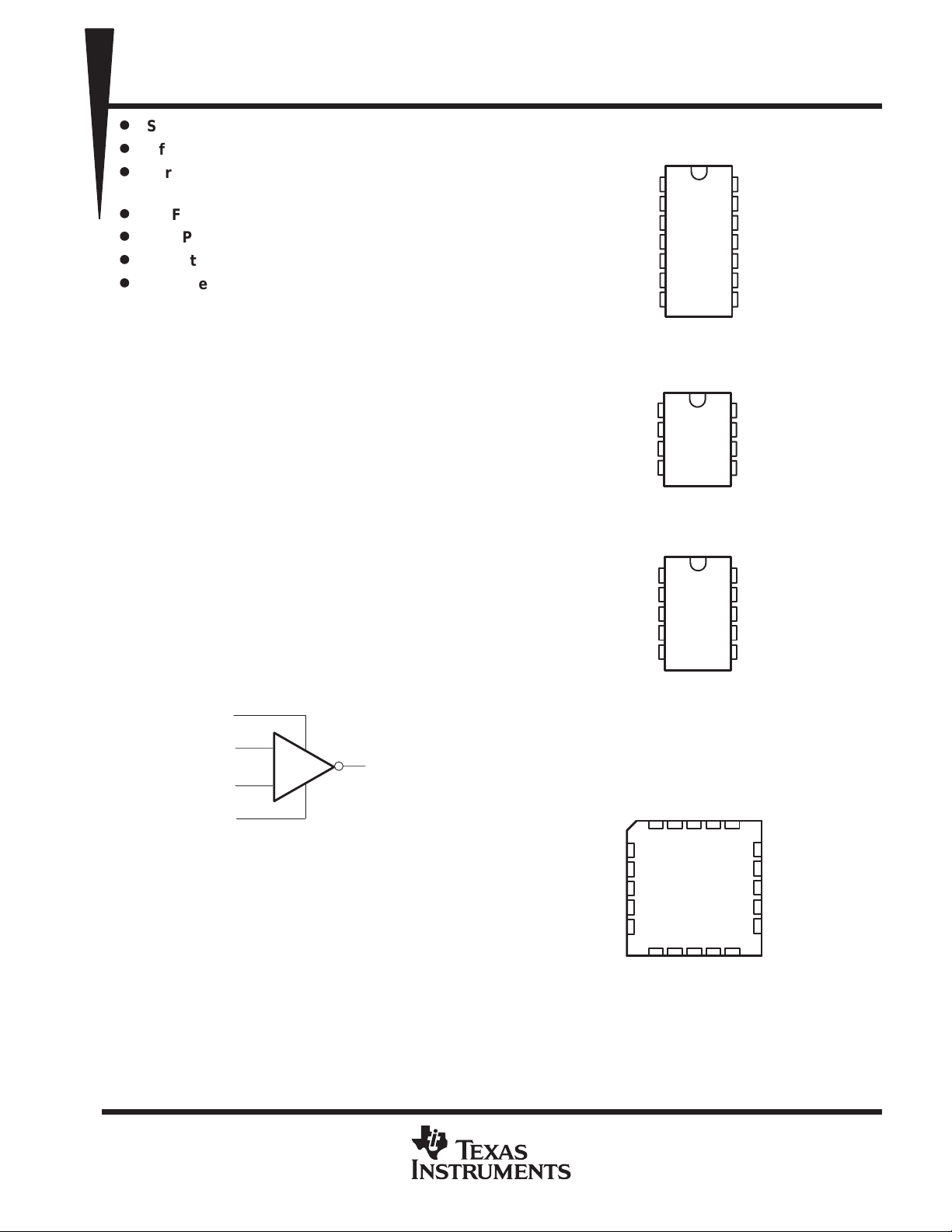
µA741M ...J PACKAGE
(TOP VIEW)
NC
1
NC
2
OFFSET N1
V
CC
µA741M ...JG PACKAGE
µA741C, µA741I . . . D, P, OR PW PACKAGE
OFFSET N1
IN+
V
CC–
3
IN–
4
IN+
5
–
6
NC
7
(TOP VIEW)
1
IN–
2
3
4
µA741M ...U PACKAGE
(TOP VIEW)
NC
14
NC
13
NC
12
V
11
OUT
10
OFFSET N2
9
NC
8
NC
8
V
7
CC+
OUT
6
OFFSET N2
5
CC+
The µA741C is characterized for operation from
0°C to 70°C. The µA741I is characterized for
operation from – 40°C to 85°C.The µA741M is
characterized for operation over the full military
temperature range of –55°C to 125°C.
symbol
OFFSET N1
IN +
IN –
OFFSET N2
+
OUT
–
NC
OFFSET N1
IN–
IN+
V
CC–
µA741M . . . FK PACKAGE
NC
IN–
NC
IN+
NC
1
2
3
4
5
(TOP VIEW)
NC
OFFSET N1
NC
3 2 1 20 19
4
5
6
7
8
910111213
NC
NC
CC–
V
NC
10
NC
9
V
8
CC+
OUT
7
OFFSET N2
6
NC
NC
18
17
16
15
14
NC
NC
V
CC+
NC
OUT
NC
PRODUCTION DATA information is current as of publication date.
Products conform to specifications per the terms of Texas Instruments
standard warranty. Production processing does not necessarily include
testing of all parameters.
NC – No internal connection
POST OFFICE BOX 655303 • DALLAS, TEXAS 75265
OFFSET N2
Copyright 2000, Texas Instruments Incorporated
1
µA741, µA741Y
CHIP
GENERAL-PURPOSE OPERATIONAL AMPLIFIERS
SLOS094B – NOVEMBER 1970 – REVISED SEPTEMBER 2000
AVAILABLE OPTIONS
PACKAGED DEVICES
T
A
0°C to 70°C µA741CD µA741CP µA741CPW µA741Y
–40°C to 85°C µA741ID µA741IP
–55°C to 125°C µA741MFK µA741MJ µA741MJG µA741MU
The D package is available taped and reeled. Add the suffix R (e.g., µA741CDR).
SMALL
OUTLINE
(D)
CHIP
CARRIER
(FK)
CERAMIC
DIP
(J)
CERAMIC
DIP
(JG)
PLASTIC
DIP
(P)
TSSOP
(PW)
FLAT
PACK
(U)
FORM
(Y)
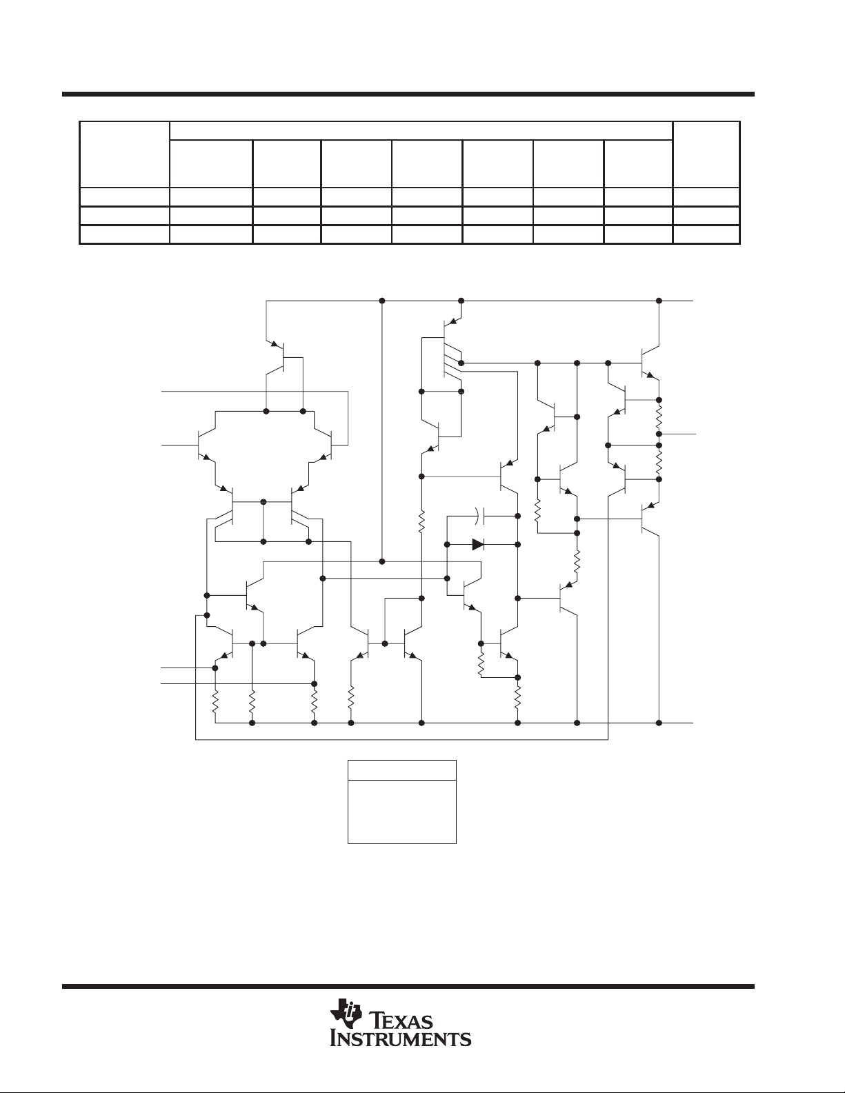
schematic
OFFSET N1
OFFSET N2
IN–
IN+
V
CC+
OUT
V
CC–
Component Count
Transistors 22
Resistors 11
Diode 1
Capacitor 1
2
POST OFFICE BOX 655303 • DALLAS, TEXAS 75265
µA741, µA741Y
GENERAL-PURPOSE OPERATIONAL AMPLIFIERS
SLOS094B – NOVEMBER 1970 – REVISED SEPTEMBER 2000
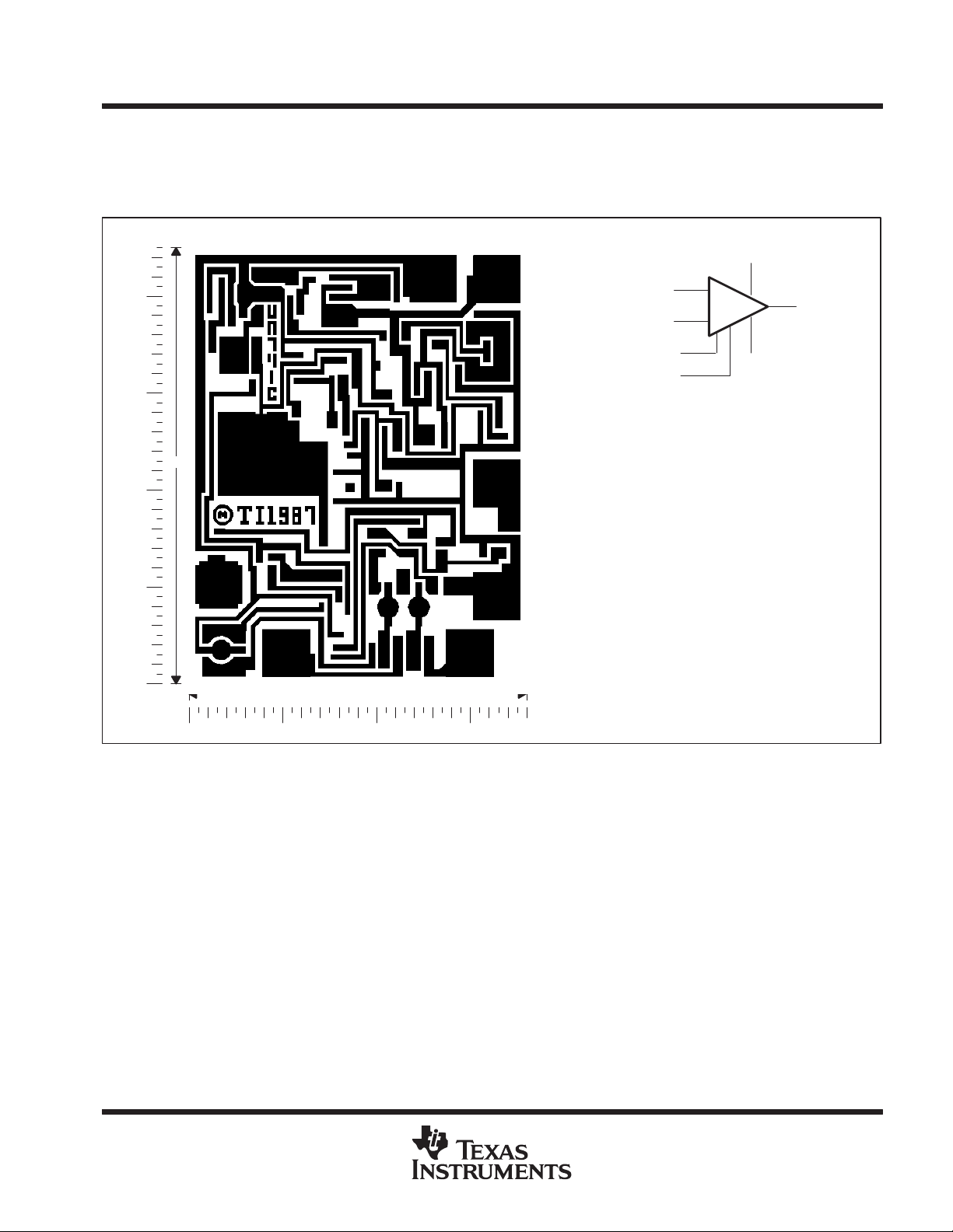
µA741Y chip information
This chip, when properly assembled, displays characteristics similar to the µA741C. Thermal compression or
ultrasonic bonding may be used on the doped-aluminum bonding pads. Chips may be mounted with conductive
epoxy or a gold-silicon preform.
BONDING PAD ASSIGNMENTS
V
CC+
(7)
+
–
V
(6)
(4)
CC–
45
(8)
(7) (6)
(5)
IN+
IN–
OFFSET N1
OFFSET N2
(3)
(2)
(1)
(5)
OUT
(1)
36
(4)
(3)(2)
CHIP THICKNESS: 15 TYPICAL
BONDING PADS: 4 × 4 MINIMUM
TJmax = 150°C.
TOLERANCES ARE ±10%.
ALL DIMENSIONS ARE IN MILS.
POST OFFICE BOX 655303 • DALLAS, TEXAS 75265
3
µA741, µA741Y
GENERAL-PURPOSE OPERATIONAL AMPLIFIERS
SLOS094B – NOVEMBER 1970 – REVISED SEPTEMBER 2000
absolute maximum ratings over operating free-air temperature range (unless otherwise noted)
µA741C µA741I µA741M UNIT
Supply voltage, V
Supply voltage, V
Differential input voltage, VID (see Note 2) ±15 ±30 ±30 V
Input voltage, VI any input (see Notes 1 and 3) ±15 ±15 ±15 V
Voltage between offset null (either OFFSET N1 or OFFSET N2) and V
Duration of output short circuit (see Note 4) unlimited unlimited unlimited
Continuous total power dissipation See Dissipation Rating Table
Operating free-air temperature range, T
Storage temperature range –65 to 150 –65 to 150 –65 to 150 °C
Case temperature for 60 seconds FK package 260 °C
Lead temperature 1,6 mm (1/16 inch) from case for 60 seconds J, JG, or U package 300 °C
Lead temperature 1,6 mm (1/16 inch) from case for 10 seconds D, P, or PW package 260 260 °C
†
Stresses beyond those listed under “absolute maximum ratings” may cause permanent damage to the device. These are stress ratings only, and
functional operation of the device at these or any other conditions beyond those indicated under “recommended operating conditions” is not
implied. Exposure to absolute-maximum-rated conditions for extended periods may affect device reliability.
NOTES: 1. All voltage values, unless otherwise noted, are with respect to the midpoint between V
2. Differential voltages are at IN+ with respect to IN–.
3. The magnitude of the input voltage must never exceed the magnitude of the supply voltage or 15 V, whichever is less.
4. The output may be shorted to ground or either power supply . For the µA741M only , the unlimited duration of the short circuit applies
at (or below) 125°C case temperature or 75°C free-air temperature.
PACKAGE
D 500 mW 5.8 mW/°C 64°C 464 mW 377 mW N/A
FK 500 mW 11.0 mW/°C 105°C 500 mW 500 mW 275 mW
J 500 mW 11.0 mW/°C 105°C 500 mW 500 mW 275 mW
JG 500 mW 8.4 mW/°C90°C 500 mW 500 mW 210 mW
P 500 mW N/A N/A 500 mW 500 mW N/A
PW 525 mW 4.2 mW/°C25°C 336 mW N/A N/A
U 500 mW 5.4 mW/°C 57°C 432 mW 351 mW 135 mW
(see Note 1) 18 22 22 V
CC+
(see Note 1) –18 –22 –22 V
CC–
±15 ±0.5 ±0.5 V
0 to 70 –40 to 85 –55 to 125 °C
and V
CC+
TA = 85°C
POWER RATING
.
CC–
POWER RATING
TA = 125°C
TA ≤ 25°C
POWER RATING
A
DERATING
FACTOR
CC–
DISSIPATION RATING TABLE
DERATE
ABOVE T
A
TA = 70°C
POWER RATING
†
4
POST OFFICE BOX 655303 • DALLAS, TEXAS 75265
PARAMETER
T
†
UNIT
VIOInput offset voltage
V
0
mV
IIOInput offset current
V
0
nA
IIBInput bias current
V
0
nA
V
V
V
V
A
gg
V/mV
CMRR
j
V
V
min
dB
k
yg y
V
±15 V
V/V
ICCSupply current
V
load
mA
PDTotal power dissipation
V
load
mW
PARAMETER
TEST CONDITIONS
UNIT
I
,
L
,
µA741, µA741Y
GENERAL-PURPOSE OPERATIONAL AMPLIFIERS
SLOS094B – NOVEMBER 1970 – REVISED SEPTEMBER 2000
electrical characteristics at specified free-air temperature, V
TEST
CONDITIONS
p
∆V
IO(adj)
ICR
OM
VD
r
i
r
o
C
i
SVS
I
OS
†
All characteristics are measured under open-loop conditions with zero common-mode input voltage unless otherwise specified. Full range for
the µA741C is 0°C to 70°C, the µA741I is –40°C to 85°C, and the µA741M is –55°C to 125°C.
NOTE 5: This typical value applies only at frequencies above a few hundred hertz because of the effects of drift and thermal feedback.
Offset voltage adjust range VO = 0 25°C ±15 ±15 mV
p
p
Common-mode input
voltage range
Maximum peak output
voltage swing
Large-signal differential
voltage amplification
Input resistance 25°C 0.3 2 0.3 2 MΩ
Output resistance VO = 0, See Note 5 25°C 75 75 Ω
Input capacitance 25°C 1.4 1.4 pF
Common-mode rejection
ratio
Supply voltage sensitivity
(∆VIO/∆VCC)
Short-circuit output current 25°C ±25 ±40 ±25 ±40 mA
pp
p
p
=
O
=
O
=
O
RL = 10 kΩ 25°C ±12 ±14 ±12 ±14
RL ≥ 10 kΩ
RL = 2 kΩ
RL ≥ 2 kΩ Full range ±10 ±10
RL ≥ 2 kΩ 25°C 20 200 50 200
VO = ±10 V
=
IC
ICR
= ±9 V to
CC
= 0,No
O
= 0,No
O
A
25°C 1 6 1 5
Full range 7.5 6
25°C 20 200 20 200
Full range 300 500
25°C 80 500 80 500
Full range 800 1500
25°C ±12 ±13 ±12 ±13
Full range ±12 ±12
Full range ±12 ±12
25°C ±10 ±13 ±10 ±13
Full range 15 25
25°C 70 90 70 90
Full range 70 70
25°C 30 150 30 150
Full range 150 150
25°C 1.7 2.8 1.7 2.8
Full range 3.3 3.3
25°C 50 85 50 85
Full range 100 100
MIN TYP MAX MIN TYP MAX
= ±15 V (unless otherwise noted)
CC±
µA741C µA741I, µA741M
µ
operating characteristics, V
t
r
SR Slew rate at unity gain
Rise time
Overshoot factor
= ±15 V, TA = 25°C
CC±
V
= 20 mV, R
CL = 100 pF,
VI = 10 V,
CL = 100 pF,
POST OFFICE BOX 655303 • DALLAS, TEXAS 75265
= 2 kΩ,
See Figure 1
RL = 2 kΩ,
See Figure 1
µA741C µA741I, µA741M
MIN TYP MAX MIN TYP MAX
0.3 0.3 µs
5% 5%
0.5 0.5 V/µs
5
µA741, µA741Y
PARAMETER
TEST CONDITIONS
UNIT
VOMMaximum peak output voltage swing
V
PARAMETER
TEST CONDITIONS
UNIT
I
,
L
,
GENERAL-PURPOSE OPERATIONAL AMPLIFIERS
SLOS094B – NOVEMBER 1970 – REVISED SEPTEMBER 2000
electrical characteristics at specified free-air temperature, V
= ±15 V, T
CC±
= 25°C (unless
A
otherwise noted)
µA741Y
MIN TYP MAX
V
IO
∆V
IO(adj)
I
IO
I
IB
V
ICR
A
VD
r
i
r
o
C
i
CMRR Common-mode rejection ratio VIC = V
k
SVS
I
OS
I
CC
P
D
†
All characteristics are measured under open-loop conditions with zero common-mode voltage unless otherwise specified.
NOTE 5: This typical value applies only at frequencies above a few hundred hertz because of the effects of drift and thermal feedback.
Input offset voltage VO = 0 1 6 mV
Offset voltage adjust range VO = 0 ±15 mV
Input offset current VO = 0 20 200 nA
Input bias current VO = 0 80 500 nA
Common-mode input voltage range ±12 ±13 V
p
Large-signal differential voltage amplification RL ≥ 2 kΩ 20 200 V/mV
Input resistance 0.3 2 MΩ
Output resistance VO = 0, See Note 5 75 Ω
Input capacitance 1.4 pF
Supply voltage sensitivity (∆VIO/∆VCC) VCC = ±9 V to ±15 V 30 150 µV/V
Short-circuit output current ±25 ±40 mA
Supply current VO = 0, No load 1.7 2.8 mA
Total power dissipation VO = 0, No load 50 85 mW
p
RL = 10 kΩ ±12 ±14
RL = 2 kΩ ±10 ±13
min 70 90 dB
ICR
operating characteristics, V
t
r
SR Slew rate at unity gain
Rise time
Overshoot factor
± = ±15 V, T
CC
= 25°C
A
V
= 20 mV, R
CL = 100 pF,
VI = 10 V,
CL = 100 pF,
= 2 kΩ,
See Figure 1
RL = 2 kΩ,
See Figure 1
µA741Y
MIN TYP MAX
0.3 µs
5%
0.5 V/µs
6
POST OFFICE BOX 655303 • DALLAS, TEXAS 75265
µA741, µA741Y
GENERAL-PURPOSE OPERATIONAL AMPLIFIERS
SLOS094B – NOVEMBER 1970 – REVISED SEPTEMBER 2000
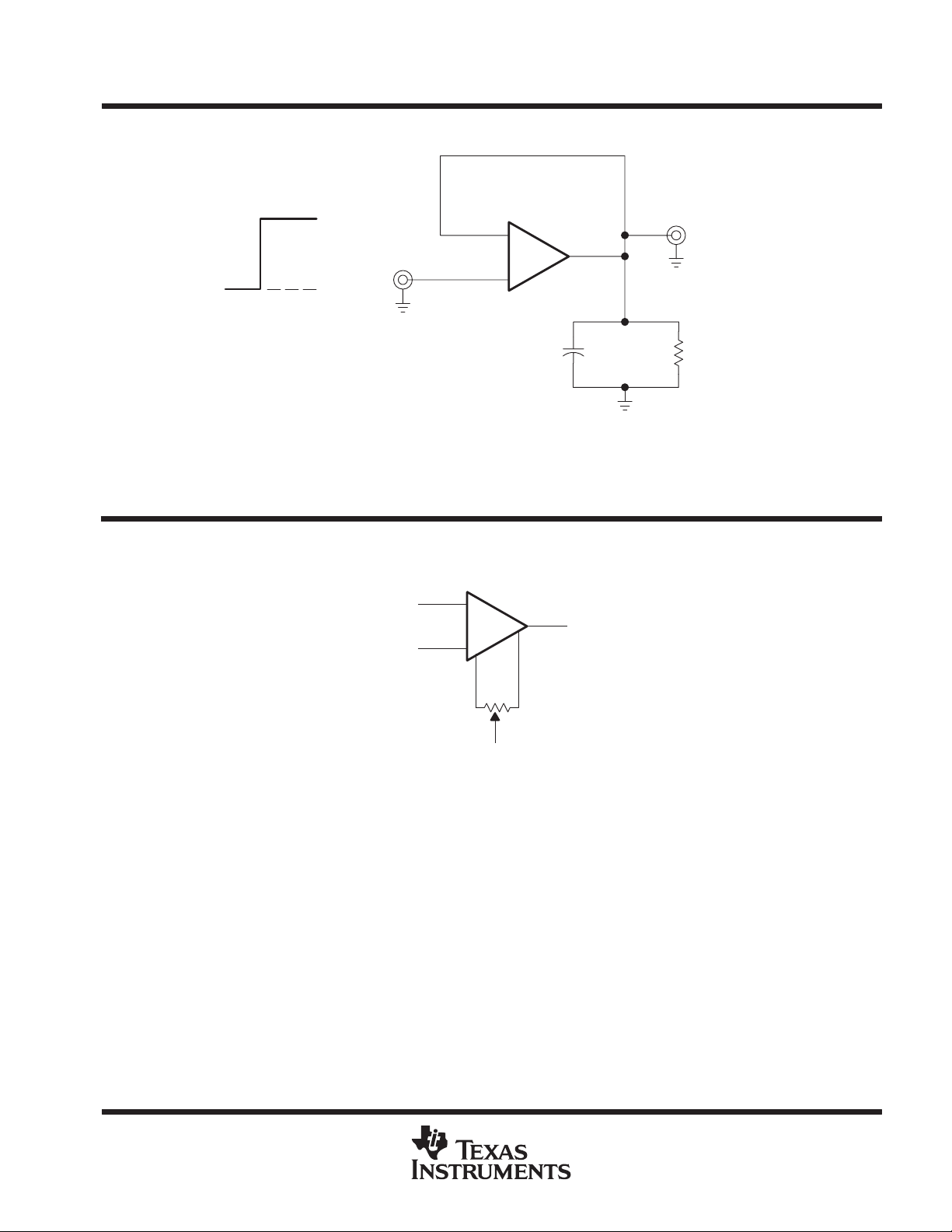
PARAMETER MEASUREMENT INFORMATION
V
I
IN
0 V
INPUT VOLTAGE
WAVEFDORM
Figure 1. Rise Time, Overshoot, and Slew Rate
–
+
CL = 100 pF
OUT
RL = 2 kΩ
TEST CIRCUIT
APPLICATION INFORMATION
Figure 2 shows a diagram for an input offset voltage null circuit.
IN+
IN–
OFFSET N1
Figure 2. Input Offset Voltage Null Circuit
+
–
10 kΩ
To V
OFFSET N2
CC –
OUT
POST OFFICE BOX 655303 • DALLAS, TEXAS 75265
7

µA741, µA741Y
GENERAL-PURPOSE OPERATIONAL AMPLIFIERS
SLOS094B – NOVEMBER 1970 – REVISED SEPTEMBER 2000
TYPICAL CHARACTERISTICS
INPUT OFFSET CURRENT
vs
FREE-AIR TEMPERATURE
100
V
= 15 V
CC+
90
V
= –15 V
CC–
80
70
60
50
40
– Input Offset Current – nA
30
IO
I
20
10
0
–60 – 20 20 60 100 140
TA – Free-Air Temperature – °C
Figure 3
†
INPUT BIAS CURRENT
vs
FREE-AIR TEMPERATURE
400
V
= 15 V
350
300
250
200
150
– Input Bias Current – nA
IB
I
100
50
12080400–40
CC+
V
= –15 V
CC–
0
–40–60 –20 20 60 100 140
0 40 80 120
TA – Free-Air Temperature – °C
Figure 4
±14
±13
±12
±11
±10
±9
±8
±7
±6
– Maximum Peak Output Voltage – V
OM
±5
V
±4
MAXIMUM PEAK OUTPUT VOLTAGE
vs
LOAD RESISTANCE
V
= 15 V
CC+
V
= –15 V
CC–
TA = 25°C
RL – Load Resistance – kΩ
Figure 5
1074210.70.40.20.1
†
Data at high and low temperatures are applicable only within the rated operating free-air temperature ranges of the various devices.
8
POST OFFICE BOX 655303 • DALLAS, TEXAS 75265

µA741, µA741Y
GENERAL-PURPOSE OPERATIONAL AMPLIFIERS
SLOS094B – NOVEMBER 1970 – REVISED SEPTEMBER 2000
TYPICAL CHARACTERISTICS
OPEN-LOOP SIGNAL DIFFERENTIAL
VOLTAGE AMPLIFICATION
vs
SUPPLY VOLTAGE
±20
±18
±16
±14
±12
±10
MAXIMUM PEAK OUTPUT VOLTAGE
vs
FREQUENCY
V
= 15 V
CC+
V
= –15 V
CC–
RL = 10 kΩ
TA = 25°C
400
200
100
VO = ±10 V
RL = 2 kΩ
TA = 25°C
±8
±6
±4
– Maximum Peak Output Voltage – V
OM
±2
V
0
100
f – Frequency – Hz
Figure 6
Voltage Amplification – dB
– Open-Loop Signal Differential
VD
A
40
– Open-Loop Signal Differential
Voltage Amplification – V/mV
20
VD
A
1M100k10k1k
10
0
OPEN-LOOP LARGE-SIGNAL DIFFERENTIAL
VOLTAGE AMPLIFICATION
vs
FREQUENCY
110
V
100
90
80
70
60
50
40
30
20
10
–10
0
10 1k 100k
f – Frequency – Hz
= 15 V
CC+
V
= –15 V
CC–
VO = ±10 V
RL = 2 kΩ
TA = 25°C
V
– Supply Voltage – V
CC±
Figure 7
10M1M10k1001
2018161412108642
POST OFFICE BOX 655303 • DALLAS, TEXAS 75265
9

µA741, µA741Y
GENERAL-PURPOSE OPERATIONAL AMPLIFIERS
SLOS094B – NOVEMBER 1970 – REVISED SEPTEMBER 2000
TYPICAL CHARACTERISTICS
COMMON-MODE REJECTION RATIO
vs
FREQUENCY
100
V
90
80
70
60
50
40
30
20
10
CMRR – Common-Mode Rejection Ratio – dB
0
10k 1M 100M1001
f – Frequency – Hz
CC+
V
CC–
BS = 10 kΩ
TA = 25°C
Figure 8
= 15 V
= –15 V
– Output Voltage – mV
O
V
28
24
20
16
12
–4
OUTPUT VOLTAGE
vs
ELAPSED TIME
90%
8
V
= 15 V
4
10%
0
t
r
t – Time − µs
CC+
V
= –15 V
CC–
RL = 2 kΩ
CL = 100 pF
TA = 25°C
2.521.510.50
Figure 9
8
6
4
2
0
–2
–4
Input and Output Voltage – V
–6
–8
VOLTAGE-FOLLOWER
LARGE-SIGNAL PULSE RESPONSE
V
= 15 V
CC+
V
= –15 V
CC–
RL = 2 kΩ
CL = 100 pF
V
O
V
I
t – Time – µs
TA = 25°C
Figure 10
9080706050403020100
10
POST OFFICE BOX 655303 • DALLAS, TEXAS 75265

PACKAGE OPTION ADDENDUM
www.ti.com
4-Jun-2007
PACKAGING INFORMATION
Orderable Device Status
(1)
Package
Type
Package
Drawing
Pins Package
Qty
Eco Plan
UA741CD ACTIVE SOIC D 8 75 Green (RoHS &
no Sb/Br)
UA741CDE4 ACTIVE SOIC D 8 75 Green (RoHS &
no Sb/Br)
UA741CDG4 ACTIVE SOIC D 8 75 Green (RoHS &
no Sb/Br)
UA741CDR ACTIVE SOIC D 8 2500 Green (RoHS &
no Sb/Br)
UA741CDRE4 ACTIVE SOIC D 8 2500 Green (RoHS &
no Sb/Br)
UA741CDRG4 ACTIVE SOIC D 8 2500 Green (RoHS &
no Sb/Br)
UA741CJG OBSOLETE CDIP JG 8 TBD Call TI Call TI
UA741CJG4 OBSOLETE CDIP JG 8 TBD Call TI Call TI
UA741CP ACTIVE PDIP P 8 50 Pb-Free
UA741CPE4 ACTIVE PDIP P 8 50 Pb-Free
UA741CPSR ACTIVE SO PS 8 2000 Green (RoHS &
no Sb/Br)
UA741CPSRE4 ACTIVE SO PS 8 2000 Green (RoHS &
no Sb/Br)
UA741CPSRG4 ACTIVE SO PS 8 2000 Green (RoHS &
no Sb/Br)
UA741MFKB OBSOLETE LCCC FK 20 TBD Call TI Call TI
UA741MJ OBSOLETE CDIP J 14 TBD Call TI Call TI
UA741MJB OBSOLETE CDIP J 14 TBD Call TI Call TI
UA741MJG OBSOLETE CDIP JG 8 TBD Call TI Call TI
UA741MJGB OBSOLETE CDIP JG 8 TBD Call TI Call TI
(1)
The marketing status values are defined as follows:
ACTIVE: Product device recommended for new designs.
LIFEBUY: TI has announced that the device will be discontinued, and a lifetime-buy period is in effect.
NRND: Not recommended for new designs. Device is in production to support existing customers, but TI does not recommend using this part in
a new design.
PREVIEW: Device has been announced but is not in production. Samples may or may not be available.
OBSOLETE: TI has discontinued the production of the device.
(RoHS)
(RoHS)
(2)
Lead/Ball Finish MSL Peak Temp
CU NIPDAU Level-1-260C-UNLIM
CU NIPDAU Level-1-260C-UNLIM
CU NIPDAU Level-1-260C-UNLIM
CU NIPDAU Level-1-260C-UNLIM
CU NIPDAU Level-1-260C-UNLIM
CU NIPDAU Level-1-260C-UNLIM
CU NIPDAU N / A for Pkg Type
CU NIPDAU N / A for Pkg Type
CU NIPDAU Level-1-260C-UNLIM
CU NIPDAU Level-1-260C-UNLIM
CU NIPDAU Level-1-260C-UNLIM
(3)
(2)
Eco Plan - The planned eco-friendly classification: Pb-Free (RoHS), Pb-Free (RoHS Exempt), or Green (RoHS & no Sb/Br) - please check
http://www.ti.com/productcontent for the latest availability information and additional product content details.
TBD: The Pb-Free/Green conversion plan has not been defined.
Pb-Free (RoHS): TI's terms "Lead-Free" or "Pb-Free" mean semiconductor products that are compatible with the current RoHS requirements
for all 6 substances, including the requirement that lead not exceed 0.1% by weight in homogeneous materials. Where designed to be soldered
at high temperatures, TI Pb-Free products are suitable for use in specified lead-free processes.
Pb-Free (RoHS Exempt): This component has a RoHS exemption for either 1) lead-based flip-chip solder bumps used between the die and
package, or 2) lead-based die adhesive used between the die and leadframe. The component is otherwise considered Pb-Free (RoHS
compatible) as defined above.
Green (RoHS & no Sb/Br): TI defines "Green" to mean Pb-Free (RoHS compatible), and free of Bromine (Br) and Antimony (Sb) based flame
retardants (Br or Sb do not exceed 0.1% by weight in homogeneous material)
(3)
MSL, Peak Temp. -- The Moisture Sensitivity Level rating according to the JEDEC industry standard classifications, and peak solder
temperature.
Addendum-Page 1

PACKAGE OPTION ADDENDUM
www.ti.com
Important Information and Disclaimer:The information provided on this page represents TI's knowledge and belief as of the date that it is
provided. TI bases its knowledge and belief on information provided by third parties, and makes no representation or warranty as to the
accuracy of such information. Efforts are underway to better integrate information from third parties. TI has taken and continues to take
reasonable steps to provide representative and accurate information but may not have conducted destructive testing or chemical analysis on
incoming materials and chemicals. TI and TI suppliers consider certain information to be proprietary, and thus CAS numbers and other limited
information may not be available for release.
In no event shall TI's liability arising out of such information exceed the total purchase price of the TI part(s) at issue in this document sold by TI
to Customer on an annual basis.
4-Jun-2007
Addendum-Page 2

PACKAGE MATERIALS INFORMATION
www.ti.com
TAPE AND REEL INFORMATION
19-Mar-2008
*All dimensions are nominal
Device Package
UA741CDR SOIC D 8 2500 330.0 12.4 6.4 5.2 2.1 8.0 12.0 Q1
UA741CPSR SO PS 8 2000 330.0 16.4 8.2 6.6 2.5 12.0 16.0 Q1
Type
Package
Drawing
Pins SPQ Reel
Diameter
(mm)
Reel
Width
W1 (mm)
A0 (mm) B0 (mm) K0 (mm) P1
(mm)W(mm)
Pin1
Quadrant
Pack Materials-Page 1

PACKAGE MATERIALS INFORMATION
www.ti.com
19-Mar-2008
*All dimensions are nominal
Device Package Type Package Drawing Pins SPQ Length (mm) Width (mm) Height (mm)
UA741CDR SOIC D 8 2500 340.5 338.1 20.6
UA741CPSR SO PS 8 2000 346.0 346.0 33.0
Pack Materials-Page 2

MECHANICAL DATA
MLCC006B – OCTOBER 1996
FK (S-CQCC-N**) LEADLESS CERAMIC CHIP CARRIER
28 TERMINAL SHOWN
A SQ
B SQ
20
22
23
24
25
19
21
12826 27
12
1314151618 17
0.020 (0,51)
0.010 (0,25)
MIN
0.342
(8,69)
0.442
0.640
0.739
0.938
1.141
A
0.358
(9,09)
0.458
(11,63)
0.660
(16,76)
0.761
(19,32)(18,78)
0.962
(24,43)
1.165
(29,59)
NO. OF
TERMINALS
**
11
10
9
8
7
6
5
432
20
28
44
52
68
84
0.020 (0,51)
0.010 (0,25)
(11,23)
(16,26)
(23,83)
(28,99)
MINMAX
0.307
(7,80)
0.406
(10,31)
0.495
(12,58)
0.495
(12,58)
0.850
(21,6)
1.047
(26,6)
0.080 (2,03)
0.064 (1,63)
B
MAX
0.358
(9,09)
0.458
(11,63)
0.560
(14,22)
0.560
(14,22)
0.858
(21,8)
1.063
(27,0)
0.055 (1,40)
0.045 (1,14)
0.028 (0,71)
0.022 (0,54)
0.050 (1,27)
NOTES: A. All linear dimensions are in inches (millimeters).
B. This drawing is subject to change without notice.
C. This package can be hermetically sealed with a metal lid.
D. The terminals are gold plated.
E. Falls within JEDEC MS-004
POST OFFICE BOX 655303 • DALLAS, TEXAS 75265
0.045 (1,14)
0.035 (0,89)
0.045 (1,14)
0.035 (0,89)
4040140/D 10/96


MECHANICAL DATA
MCER001A – JANUARY 1995 – REVISED JANUARY 1997
JG (R-GDIP-T8) CERAMIC DUAL-IN-LINE
0.400 (10,16)
0.355 (9,00)
0.063 (1,60)
0.015 (0,38)
0.100 (2,54)
8
1
5
4
0.065 (1,65)
0.045 (1,14)
0.020 (0,51) MIN
0.023 (0,58)
0.015 (0,38)
0.280 (7,11)
0.245 (6,22)
0.310 (7,87)
0.290 (7,37)
0.200 (5,08) MAX
Seating Plane
0.130 (3,30) MIN
0°–15°
0.014 (0,36)
0.008 (0,20)
NOTES: A. All linear dimensions are in inches (millimeters).
B. This drawing is subject to change without notice.
C. This package can be hermetically sealed with a ceramic lid using glass frit.
D. Index point is provided on cap for terminal identification.
E. Falls within MIL STD 1835 GDIP1-T8
4040107/C 08/96
POST OFFICE BOX 655303 • DALLAS, TEXAS 75265

MECHANICAL DATA
MPDI001A – JANUARY 1995 – REVISED JUNE 1999
P (R-PDIP-T8) PLASTIC DUAL-IN-LINE
0.400 (10,60)
0.355 (9,02)
8
5
0.260 (6,60)
0.240 (6,10)
1
0.021 (0,53)
0.015 (0,38)
NOTES: A. All linear dimensions are in inches (millimeters).
B. This drawing is subject to change without notice.
C. Falls within JEDEC MS-001
4
0.070 (1,78) MAX
0.020 (0,51) MIN
0.200 (5,08) MAX
0.125 (3,18) MIN
0.100 (2,54)
0.010 (0,25)
Seating Plane
M
0.325 (8,26)
0.300 (7,62)
0.015 (0,38)
Gage Plane
0.010 (0,25) NOM
0.430 (10,92)
MAX
4040082/D 05/98
For the latest package information, go to http://www.ti.com/sc/docs/package/pkg_info.htm
POST OFFICE BOX 655303 • DALLAS, TEXAS 75265

IMPORTANT NOTICE
Texas Instruments Incorporated and its subsidiaries (TI) reserve the right to make corrections, modifications, enhancements, improvements,
and other changes to its products and services at any time and to discontinue any product or service without notice. Customers should
obtain the latest relevant information before placing orders and should verify that such information is current and complete. All products are
sold subject to TI’s terms and conditions of sale supplied at the time of order acknowledgment.
TI warrants performance of its hardware products to the specifications applicable at the time of sale in accordance with TI’s standard
warranty. Testing and other quality control techniques are used to the extent TI deems necessary to support this warranty. Except where
mandated by government requirements, testing of all parameters of each product is not necessarily performed.
TI assumes no liability for applications assistance or customer product design. Customers are responsible for their products and
applications using TI components. To minimize the risks associated with customer products and applications, customers should provide
adequate design and operating safeguards.
TI does not warrant or represent that any license, either express or implied, is granted under any TI patent right, copyright, mask work right,
or other TI intellectual property right relating to any combination, machine, or process in which TI products or services are used. Information
published by TI regarding third-party products or services does not constitute a license from TI to use such products or services or a
warranty or endorsement thereof. Use of such information may require a license from a third party under the patents or other intellectual
property of the third party, or a license from TI under the patents or other intellectual property of TI.
Reproduction of TI information in TI data books or data sheets is permissible only if reproduction is without alteration and is accompanied
by all associated warranties, conditions, limitations, and notices. Reproduction of this information with alteration is an unfair and deceptive
business practice. TI is not responsible or liable for such altered documentation. Information of third parties may be subject to additional
restrictions.
Resale of TI products or services with statements different from or beyond the parameters stated by TI for that product or service voids all
express and any implied warranties for the associated TI product or service and is an unfair and deceptive business practice. TI is not
responsible or liable for any such statements.
TI products are not authorized for use in safety-critical applications (such as life support) where a failure of the TI product would reasonably
be expected to cause severe personal injury or death, unless officers of the parties have executed an agreement specifically governing
such use. Buyers represent that they have all necessary expertise in the safety and regulatory ramifications of their applications, and
acknowledge and agree that they are solely responsible for all legal, regulatory and safety-related requirements concerning their products
and any use of TI products in such safety-critical applications, notwithstanding any applications-related information or support that may be
provided by TI. Further, Buyers must fully indemnify TI and its representatives against any damages arising out of the use of TI products in
such safety-critical applications.
TI products are neither designed nor intended for use in military/aerospace applications or environments unless the TI products are
specifically designated by TI as military-grade or "enhanced plastic." Only products designated by TI as military-grade meet military
specifications. Buyers acknowledge and agree that any such use of TI products which TI has not designated as military-grade is solely at
the Buyer's risk, and that they are solely responsible for compliance with all legal and regulatory requirements in connection with such use.
TI products are neither designed nor intended for use in automotive applications or environments unless the specific TI products are
designated by TI as compliant with ISO/TS 16949 requirements. Buyers acknowledge and agree that, if they use any non-designated
products in automotive applications, TI will not be responsible for any failure to meet such requirements.
Following are URLs where you can obtain information on other Texas Instruments products and application solutions:
Products Applications
Amplifiers amplifier.ti.com Audio www.ti.com/audio
Data Converters dataconverter.ti.com Automotive www.ti.com/automotive
DSP dsp.ti.com Broadband www.ti.com/broadband
Clocks and Timers www.ti.com/clocks Digital Control www.ti.com/digitalcontrol
Interface interface.ti.com Medical www.ti.com/medical
Logic logic.ti.com Military www.ti.com/military
Power Mgmt power.ti.com Optical Networking www.ti.com/opticalnetwork
Microcontrollers microcontroller.ti.com Security www.ti.com/security
RFID www.ti-rfid.com Telephony www.ti.com/telephony
RF/IF and ZigBee® Solutions www.ti.com/lprf Video & Imaging www.ti.com/video
Mailing Address: Texas Instruments, Post Office Box 655303, Dallas, Texas 75265
Copyright © 2008, Texas Instruments Incorporated
Wireless www.ti.com/wireless
 Loading...