

SN54ALS273, SN74ALS273
OCTAL D-TYPE FLIP-FLOPS
WITH CLEAR
SDAS218A – APRIL 1982 – REVISED DECEMBER 1994
Copyright 1994, Texas Instruments Incorporated
1
POST OFFICE BOX 655303 • DALLAS, TEXAS 75265
• Contain Eight Flip-Flops With Single-Rail
Outputs
• Buffered Clock and Direct-Clear Inputs
• Individual Data Input to Each Flip-Flop
• Applications Include:
Buffer/Storage Registers
Shift Registers
Pattern Generators
• Package Options Include Plastic
Small-Outline (DW) Packages, Ceramic
Chip Carriers (FK), and Standard Plastic (N)
and Ceramic (J) 300-mil DIPs
description
These octal positive-edge-triggered flip-flops
utilize TTL circuitry to implement D-type flip-flop
logic with a direct-clear (CLR
) input.
Information at the data (D) inputs meeting the
setup-time requirements is transferred to the
Q outputs on the positive-going edge of the clock
(CLK) pulse. Clock triggering occurs at a particular
voltage level and is not directly related to the
transition time of the positive-going pulse. When
CLK is at either the high or low level, the D input
signal has no effect at the output.
The SN54ALS273 is characterized for operation
over the full military temperature range of –55°C
to 125°C. The SN74ALS273 is characterized for
operation from 0°C to 70°C.
FUNCTION TABLE
(each flip-flop)
INPUTS
OUTPUT
CLR
CLK D
OUTPUT
Q
L X X L
H ↑ HH
H↑LL
HH or L X Q
0
1
2
3
4
5
6
7
8
9
10
20
19
18
17
16
15
14
13
12
11
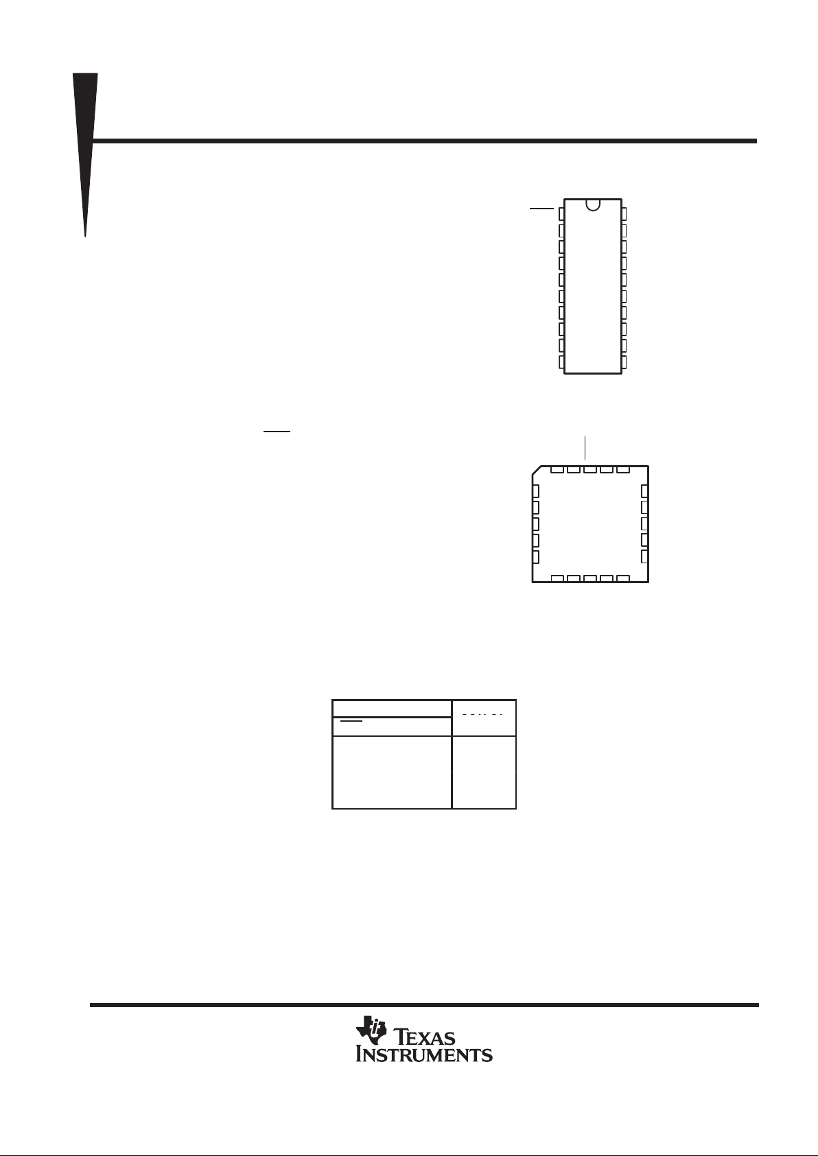
CLR
1Q
1D
2D
2Q
3Q
3D
4D
4Q
GND
V
CC
8Q
8D
7D
7Q
6Q
6D
5D
5Q
CLK
SN54ALS273 ...J PACKAGE
SN74ALS273 . . . DW OR N PACKAGE
(TOP VIEW)
3212019
910111213
4
5
6
7
8
18
17
16
15
14
8D
7D
7Q
6Q
6D
2D
2Q
3Q
3D
4D
1D1QCLR
5Q
5D
8Q
4Q
GND
CLK
V
CC
SN54ALS273 . . . FK PACKAGE
(TOP VIEW)
PRODUCTION DATA information is current as of publication date.
Products conform to specifications per the terms of Texas Instruments
standard warranty. Production processing does not necessarily include
testing of all parameters.
SN54ALS273, SN74ALS273
OCTAL D-TYPE FLIP-FLOPS
WITH CLEAR
SDAS218A – APRIL 1982 – REVISED DECEMBER 1994
2
POST OFFICE BOX 655303 • DALLAS, TEXAS 75265
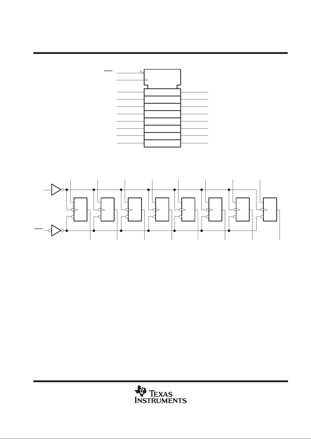
logic symbol
†
1D
3
1D
11
CLK
C1
R
1
1Q
2
4
2D
2Q
5
7
3D
3Q
6
8
4D
4Q
9
13
5D
5Q
12
14
6D
6Q
15
17
7D
7Q
16
18
8D
8Q
19
CLR
†
This symbol is in accordance with ANSI/IEEE Std 91-1984 and IEC Publication 617-12.
logic diagram (positive logic)
CLK
1D
3
1D
C1
R
1Q
2
2D
4
1D
C1
R
2Q
5
3D
7
1D
C1
R
3Q
6
4D
8
1D
C1
R
4Q
9
5D
13
1D
C1
R
5Q
12
6D
14
1D
C1
R
6Q
15
7D
17
1D
C1
R
7Q
16
8D
18
1D
C1
R
8Q
19
CLR
11
1
absolute maximum ratings over operating free-air temperature range (unless otherwise noted)
‡
Supply voltage, V
CC
7 V. . . . . . . . . . . . . . . . . . . . . . . . . . . . . . . . . . . . . . . . . . . . . . . . . . . . . . . . . . . . . . . . . . . . . . . .
Input voltage, V
I
7 V. . . . . . . . . . . . . . . . . . . . . . . . . . . . . . . . . . . . . . . . . . . . . . . . . . . . . . . . . . . . . . . . . . . . . . . . . . . .
Operating free-air temperature range, T
A
: SN54ALS273 –55°C to 125°C. . . . . . . . . . . . . . . . . . . . . . . . . . . . .
SN74ALS273 0°C to 70°C. . . . . . . . . . . . . . . . . . . . . . . . . . . . . . . . .
Storage temperature range –65°C to 150°C. . . . . . . . . . . . . . . . . . . . . . . . . . . . . . . . . . . . . . . . . . . . . . . . . . . . . . .
‡
Stresses beyond those listed under “absolute maximum ratings” may cause permanent damage to the device. These are stress ratings only, and
functional operation of the device at these or any other conditions beyond those indicated under “recommended operating conditions” is not
implied. Exposure to absolute-maximum-rated conditions for extended periods may affect device reliability.
 Loading...