

Texas Instruments 8413401FA Datasheet
SN54ALS153, SN74ALS153, SN74AS153
DUAL 1-OF-4 DATA SELECTORS/MULTIPLEXERS
SDAS206A – APRIL 1982 – REVISED DECEMBER 1994
Copyright 1994, Texas Instruments Incorporated
1
POST OFFICE BOX 655303 • DALLAS, TEXAS 75265
• Permit Multiplexing From n Lines to
One Line
• Perform Parallel-to-Serial Conversion
• Strobe (Enable) Line Provided for
Cascading (n Lines to n Lines)
• ′ALS253 and SN74AS253A Are 3-State
Versions of These Parts
• Package Options Include Plastic
Small-Outline (D) Packages, Ceramic Chip
Carriers (FK), and Standard Plastic (N) and
Ceramic (J) 300-mil DIPs
description
These dual 1-of-4 data selectors/multiplexers
contain inverters and drivers to supply full binary
decoding data selection to the AND-OR gates.
Separate strobe (G
) inputs are provided for each
of the two 4-line sections.
The SN54ALS153 is characterized for operation
over the full military temperature range of –55°C
to 125°C. The SN74ALS153 and SN74AS153 are
characterized for operation from 0°C to 70°C.
FUNCTION TABLE
INPUTS
SELECT DATA
STROBE
OUTPUT
B A C0 C1 C2 C3
G
Y
X X X X X X H L
L LLXXX L L
LLHXXX L H
LHXLXX L L
LHXHXX L H
HLXXLX L L
HLXXHX L H
HHXXXL L L
HHXXXH L H
Select inputs A and B are common to both sections.
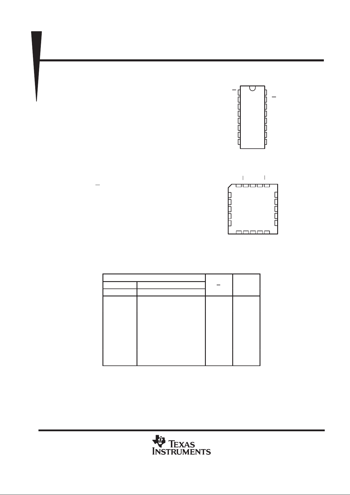
SN54ALS153 ...J PACKAGE
SN74ALS153, SN74AS153 ...D OR N PACKAGE
(TOP VIEW)
3212019
910111213
4
5
6
7
8
18
17
16
15
14
A
2C3
NC
2C2
2C1
1C3
1C2
NC
1C1
1C0
SN54ALS153 . . . FK PACKAGE
(TOP VIEW)
B1GNC
2Y
2C0
2G
1Y
GND
NC
NC – No internal connection
V
CC
1
2
3
4
5
6
7
8
16
15
14
13
12
11
10
9
1G
B
1C3
1C2
1C1
1C0
1Y
GND
V
CC
2G
A
2C3
2C2
2C1
2C0
2Y
PRODUCTION DATA information is current as of publication date.
Products conform to specifications per the terms of Texas Instruments
standard warranty. Production processing does not necessarily include
testing of all parameters.
SN54ALS153, SN74ALS153, SN74AS153
DUAL 1-OF-4 DATA SELECTORS/MULTIPLEXERS
SDAS206A – APRIL 1982 – REVISED DECEMBER 1994
2
POST OFFICE BOX 655303 • DALLAS, TEXAS 75265
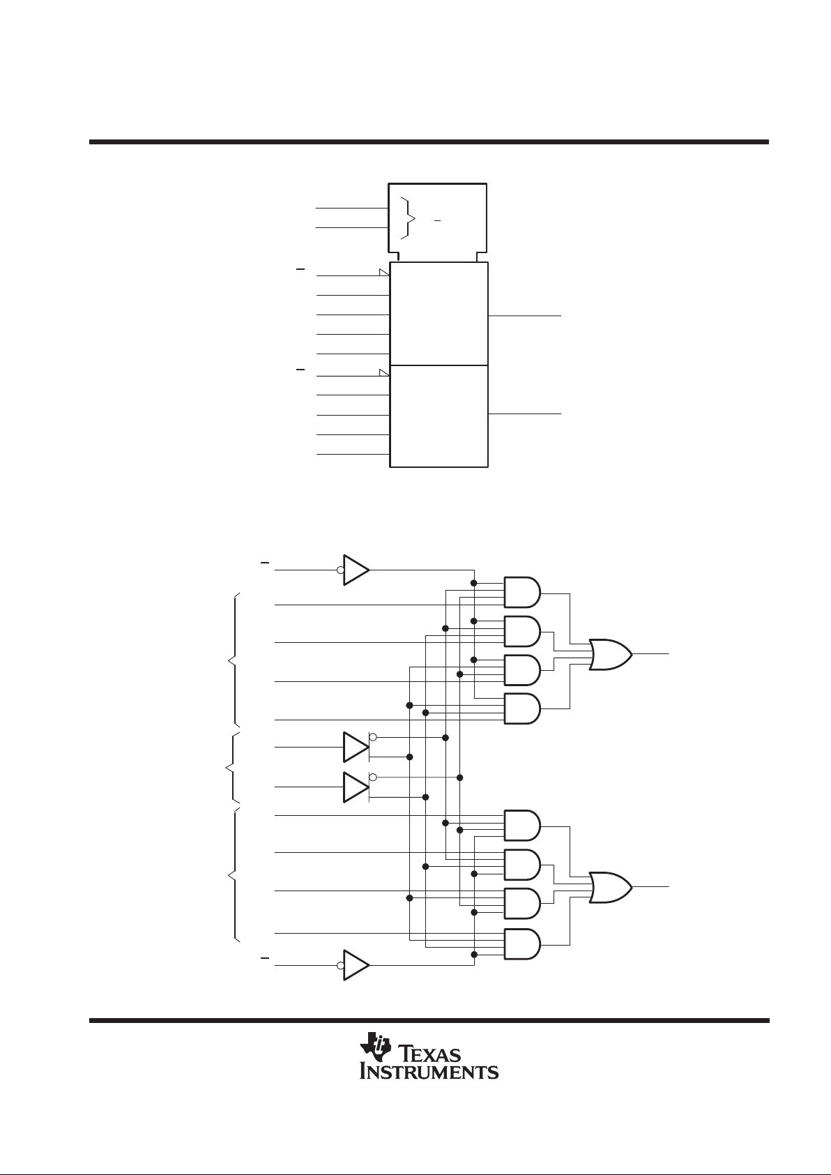
logic symbol
†
G
MUX
0
3
0
14
A
1
2
B
EN
1
15
1Y
7
0
6
1C0
1
5
1C1
2
4
1C2
3
3
1C3
10
2C0
11
2C1
12
2C2
13
2C3
2Y
9
1G
2G
†
This symbol is in accordance with ANSI/IEEE Std 91-1984 and IEC Publication 617-12.
Pin numbers shown are for the D, J, and N packages.
logic diagram (positive logic)
Data 2
Select
Data 1
2G
2C3
2C2
2C1
2C0
A
B
1C3
1C2
1C1
1C0
1G
1Y
1
6
5
4
3
2
14
10
11
12
13
15
7
2Y
9
Pin numbers shown are for the D, J, and N packages.
SN54ALS153, SN74ALS153, SN74AS153
DUAL 1-OF-4 DATA SELECTORS/MULTIPLEXERS
SDAS206A – APRIL 1982 – REVISED DECEMBER 1994
3
POST OFFICE BOX 655303 • DALLAS, TEXAS 75265
absolute maximum ratings over operating free-air temperature range (unless otherwise noted)
†
Supply voltage, V
CC
7 V. . . . . . . . . . . . . . . . . . . . . . . . . . . . . . . . . . . . . . . . . . . . . . . . . . . . . . . . . . . . . . . . . . . . . . . .
Input voltage, V
I
7 V. . . . . . . . . . . . . . . . . . . . . . . . . . . . . . . . . . . . . . . . . . . . . . . . . . . . . . . . . . . . . . . . . . . . . . . . . . . .
Operating free-air temperature range, T
A
: SN54ALS153 –55°C to 125°C. . . . . . . . . . . . . . . . . . . . . . . . . . . . .
SN74ALS153 0°C to 70°C. . . . . . . . . . . . . . . . . . . . . . . . . . . . . . . . .
Storage temperature range –65°C to 150°C. . . . . . . . . . . . . . . . . . . . . . . . . . . . . . . . . . . . . . . . . . . . . . . . . . . . . . .
†
Stresses beyond those listed under “absolute maximum ratings” may cause permanent damage to the device. These are stress ratings only, and
functional operation of the device at these or any other conditions beyond those indicated under “recommended operating conditions” is not
implied. Exposure to absolute-maximum-rated conditions for extended periods may affect device reliability.
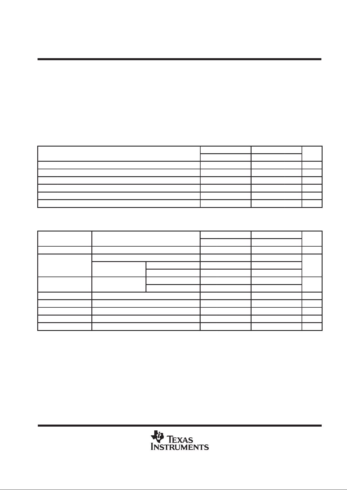
recommended operating conditions
SN54ALS153 SN74ALS153
MIN NOM MAX MIN NOM MAX
UNIT
V
CC
Supply voltage 4.5 5 5.5 4.5 5 5.5 V
V
IH
High-level input voltage 2 2 V
V
IL
Low-level input voltage 0.7 0.8 V
I
OH
High-level output current –1 –2.6 mA
I
OL
Low-level output current 12 24 mA
T
A
Operating free-air temperature –55 125 0 70 °C
electrical characteristics over recommended operating free-air temperature range (unless
otherwise noted)
SN54ALS153 SN74ALS153
PARAMETER
TEST CONDITIONS
MIN TYP‡MAX MIN TYP‡MAX
UNIT
V
IK
VCC = 4.5 V, II = –18 mA –1.5 –1.5 V
VCC = 4.5 V to 5.5 V, IOH = –0.4 mA VCC –2 VCC –2
V
OH
IOH = –1 mA 2.4 3.3
V
V
CC
=
4.5 V
IOH = –2.6 mA 2.4 3.2
IOL = 12 mA 0.25 0.4 0.25 0.4
V
OL
V
CC
= 4.5
V
IOL = 24 mA 0.35 0.5
V
I
I
VCC = 5.5 V, VI = 7 V 0.1 0.1 mA
I
IH
VCC = 5.5 V, VI = 2.7 V 20 20 µA
I
IL
VCC = 5.5 V, VI = 0.4 V –0.1 –0.1 mA
I
O
§
VCC = 5.5 V, VO = 2.25 V –20 –112 –30 –112 mA
I
CC
VCC = 5.5 V, All inputs at 4.5 V 7.5 14 7.5 14 mA
‡
All typical values are at VCC = 5 V, TA = 25°C.
§
The output conditions have been chosen to produce a current that closely approximates one half of the true short-circuit output current, IOS.
 Loading...