

Texas Instruments CY74FCT16827CTPVC, CY74FCT16827CTPACT, CY74FCT16827CTPAC, CY74FCT16827ATPVCT, CY74FCT16827ATPVC Datasheet
...
20-Bit Buffers/Line Drivers
CY74FCT16827T
CY74FCT162827T
Data sheet acquired from Cypress Semiconductor Corporation.
Data sheet modified to remove devices not offered.
SCCS064 - August 1994 - Revised March 2000
Copyright © 2000, Texas Instruments Incorporated
1CY74FCT162827T
Features
• FCT-E speed at 3.2 ns
• Power-off disable outputs permits live insertion
• Edge-rate control circuitry for significantly improved
noise characteristics
• Typical output skew < 250 ps
• ESD > 2000V
• TSSOP (19.6-mil pitch) and SSOP (25-mil pitch)
packages
• Industrial temperature range of −40˚C to +85˚C
•V
CC
= 5V ± 10%
CY74FCT16827T Features:
• 64 mA sink current, 32 mA source current
• Typical V
OLP
(ground bounce) <1.0V at VCC = 5V,
TA = 25˚C
CY74FCT162827T Features:
• Balanced 24 mA output drivers
• Reduced system switching noise
• Typical V
OLP
(ground bounce) <0.6V at VCC = 5V,
TA= 25˚C
Functional Description
The CY74FCT16827T 20-bit buffer/line driver and the
CY74FCT162827T 20-bit buffer/line driver provide
high-performance bus interf ace b uff ering for wide data/address
pathsor busescarrying parity .Thesepartscanbeusedas a single
20-bit buffer or two 10-bit buff ers. Each 10-bit buff er has a pair of
NANDed
OEforincreasedflexibility. The outputs are designed with
a power-off disable f eature to allow f or liv e insertion of boards.
The CY74FCT16827T is ideally suited for driving
high-capacitance loads and low-impedance backplanes.
The CY74FCT162827T has 24-mA balanced output drivers
with current-limiting resistors in the outputs. This reduces the
need for external terminating resistors and provides for
minimal undershoot and reduced ground bounce. The
CY74FCT162827T is ideal for driving transmission lines.
GND
Logic Block Diagrams Pin Configuration
1
2
3
4
5
6
7
8
9
10
11
12
33
32
31
30
29
36
35
1OE1
34
SSOP/TSSOP
Top View
1Y1
13
14
15
16
17
18
19
20
21
22
23
24
45
44
43
42
41
37
38
39
40
48
47
46
1A1
1OE1
1Y1
1Y2
1Y3
1Y4
1A1
1A2
1A3
1A4
1OE2
GND
GND
V
CC
2Y3
2Y4
2Y1
2Y2
1A6
V
CC
GND
GND
2OE1
FCT16827-1
1OE2
TO 9 OTHER CHANNELS
2A1
2OE1
TO 9 OTHER CHANNELS
2OE2
2Y1
1Y5
1Y6
1Y7
1Y8
1Y9
1Y10
2Y5
2Y9
2Y7
2Y8
V
CC
2Y6
2Y10
GND
25
26
27
28
55
54
53
52
51
50
49
56
1A5
1A7
1A9
1A8
1A10
2A3
2A4
2A2
GND
2A5
2A9
2A7
2A8
V
CC
2A6
2A10
2A1
GND
2OE2
FCT16827-2
FCT16827-3

CY74FCT16827T
CY74FCT162827T
2
Maximum Ratings
[2, 3]
(Above which the useful life may be impaired. For user
guidelines, not tested.)
Storage Temperature............................... −55°C to +125°C
Ambient Temperature with
Power Applied.......................................... −55°C to +125°C
DC Input Voltage .................................................−0.5V to +7.0V
DC Output Voltage..............................................−0.5V to +7.0V
DC Output Current
(Maximum Sink Current/Pin)...........................−60 to +120 mA
Power Dissipation..........................................................1.0W
Static Discharge Voltage............................................>2001V
(per MIL-STD-883, Method 3015)
Pin Description
Name Description
OE Output Enable Inputs (Active LOW)
A Data Inputs
Y Three-State Outputs
Function Table
[1]
Inputs Outputs
OE
1
OE
2
A Y
L L L L
L L H H
H X X Z
X H X Z
Operating Range
Range
Ambient
Temperature V
CC
Industrial −40°C to +85°C 5V ± 10%
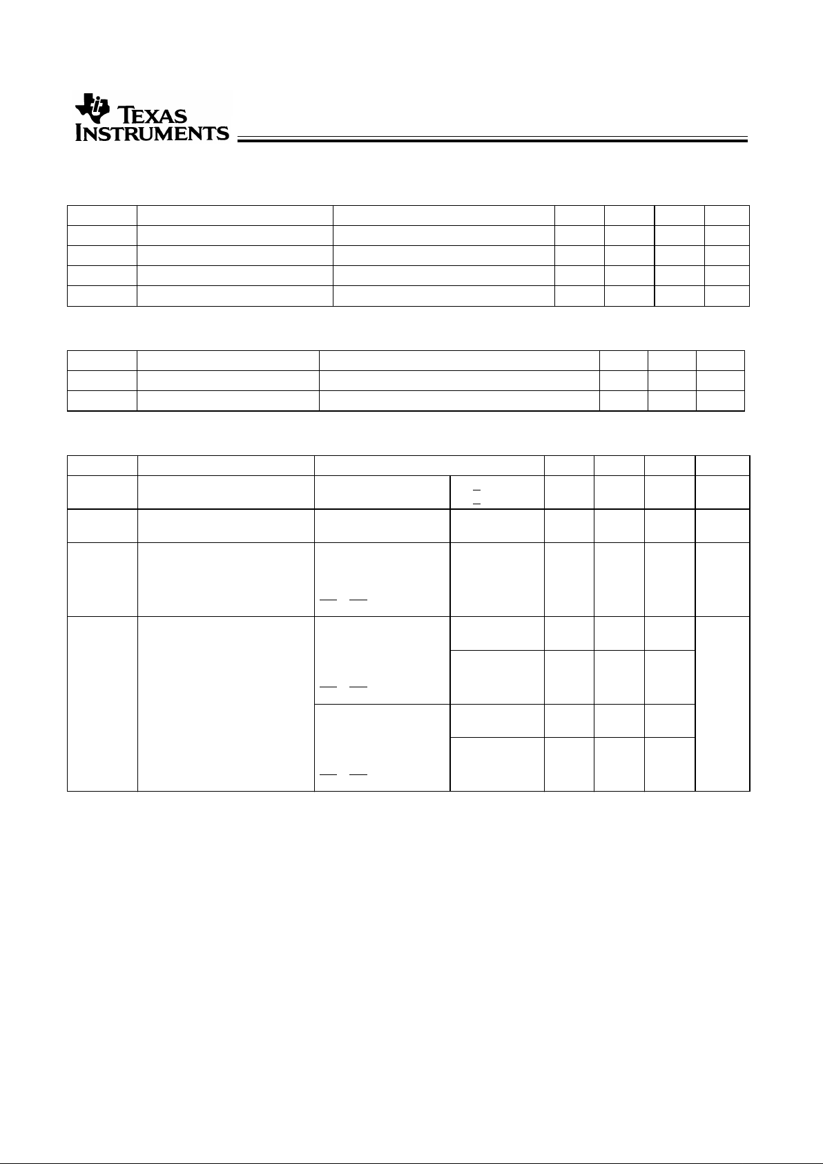
Electrical Characteristics Over the Operating Range
Parameter Description Test Conditions Min. Typ.
[4]
Max. Unit
V
IH
Input HIGH Voltage 2.0 V
V
IL
Input LOW Voltage 0.8 V
V
H
Input Hysteresis
[5]
100 mV
V
IK
Input Clamp Diode Voltage VCC=Min., IIN=−18 mA −0.7 −1.2 V
I
IH
Input HIGH Current VCC=Max., VI=V
CC
±1 µA
I
IL
Input LOW Current VCC=Max., VI=GND ±1 µA
I
OZH
High Impedance Output
Current (Three-State Output pins)
VCC=Max., V
OUT
=2.7V ±1 µA
I
OZL
High Impedance Output
Current (Three-State Output pins)
VCC=Max., V
OUT
=0.5V ±1 µA
I
OS
Short Circuit Current
[6]
VCC=Max., V
OUT
=GND −80 −140 −200 mA
I
O
Output Drive Current
[6]
VCC=Max., V
OUT
=2.5V −50 −180 mA
I
OFF
Power-Off Disable VCC=0V, V
OUT
≤4.5V
[7]
±1 µA
Output Drive Characteristics for CY74FCT16827T
Parameter Description Test Conditions Min. Typ.
[4]
Max. Unit
V
OH
Output HIGH Voltage VCC=Min., IOH=−3 mA 2.5 3.5 V
VCC=Min., IOH=−15 mA 2.4 3.5
VCC=Min., IOH=−32 mA 2.0 3.0
V
OL
Output LOW Voltage VCC=Min., IOL=64 mA 0.2 0.55 V
1. H = HIGH Voltage Level. L = LOW Voltage Level. X = Don’t Care.Z = HIGH Impedance.
2. Operation beyond the limits set forth may impair the useful life of the device. Unless noted, these limits are over the operating free-air temperature range.
3. Unused inputs must always be connected to an appropriate logic voltage level, preferably either VCC or ground.
4. Typical values are at V
CC
= 5.0V, TA= +25˚C ambient.
5. This parameter is specified but not tested.
6. Not more than one output should be shorted at a time. Duration ofshort should not exceedonesecond. The use of high-speed test apparatus and/or sample
and hold techniques are preferablein order to minimize internal chip heating and more accurately reflect operationalvalues. Otherwise prolonged shorting of
a high output may raise the chip temperature well above normal and thereby cause invalid readings in other parametric tests. In any sequence of parameter
tests, I
OS
tests should be performed last.
7. Tested at +25˚C.
CY74FCT16827T
CY74FCT162827T
3
Output Drive Characteristics for CY74FCT162827T
Parameter Description Test Conditions Min. Typ.
[4]
Max. Unit
I
ODL
Output LOW Current
[6]
VCC=5V, VIN=VIH or VIL, V
OUT
=1.5V 60 115 150 mA
I
ODH
Output HIGH Current
[6]
VCC=5V, VIN=VIH or VIL, V
OUT
=1.5V −60 −115 −150 mA
V
OH
Output HIGH Voltage VCC=Min., IOH=−24 mA 2.4 3.3 V
V
OL
Output LOW Voltage VCC=Min., IOL=24 mA 0.3 0.55 V
Capacitance
[5]
(TA = +25˚C, f = 1.0 MHz)
Parameter Description Test Conditions Typ.
[4]
Max. Unit
C
IN
Input Capacitance VIN = 0V 4.5 6.0 pF
C
OUT
Output Capacitance V
OUT
= 0V 5.5 8.0 pF
Power Supply Characteristics
Parameter Description Test Conditions Min. Typ.
[4]
Max. Unit
I
CC
Quiescent Power Supply
Current
VCC=Max. VIN<0.2V,
V
IN>VCC
−0.2V
— 5 500 µA
∆I
CC
Quiescent Power Supply
Current (TTL inputs HIGH)
VCC=Max. VIN=3.4V
[8]
— 0.5 1.5 mA
I
CCD
Dynamic Power Supply
Current
[9]
VCC=Max.,
One Input Toggling,
50% Duty Cycle,
Outputs Open,
OE1=OE2=GND,
VIN=VCC or
V
IN
=GND
— 60 100 µA/MHz
I
C
Total Power Supply Current
[10]
VCC=Max.,
f
1
=10 MHz,
50% Duty Cycle,
Outputs Open,
One Bit Toggling,
OE1=OE2=GND
VIN=VCC or
V
IN
=GND
— 0.6 1.5 mA
VIN=3.4V or
V
IN
=GND
— 0.9 2.3
VCC=Max.,
f
1
=2.5 MHz,
50% Duty Cycle,
Outputs Open,
Twenty Bits Toggling,
OE1=OE2=GND
VIN=VCC or
V
IN
=GND
— 3.0 5.5
[11]
VIN=3.4V or
V
IN
=GND
— 8.0 20.5
[11]
Notes:
8. Per TTL driven input (V
IN
=3.4V); all other inputs at VCC or GND.
9. This parameter is not directly testable, but is derived for use in Total Power Supply calculations.
10. I
C
=I
QUIESCENT
+ I
INPUTS
+ I
DYNAMIC
IC=ICC+∆ICCDHNT+I
CCD(f0
/2 + f1N1)
I
CC
= Quiescent Current with CMOS input levels
∆I
CC
= Power Supply Current for a TTL HIGH input (VIN=3.4V)
D
H
= Duty Cycle for TTL inputs HIGH
N
T
= Number of TTL inputs at D
H
I
CCD
= Dynamic Current caused by an input transition pair (HLH or LHL)
f
0
= Clock frequency for registered devices, otherwise zero
f
1
= Input signal frequency
N
1
= Number of inputs changing at f
1
All currents are in milliamps and all frequencies are in megahertz.
11. Values for these conditions are examples of the I
CC
formula. These limits are specified but not tested.
 Loading...