

Texas Instruments CY74FCT16646TPVCT, CY74FCT16646TPVC, CY74FCT16646ETPVCT, CY74FCT16646ETPVC, CY74FCT16646CTPVCT Datasheet
...
16-Bit Registered Transceivers
CY74FCT16646T
CY74FCT162646T
SCCS060 - August 1994 - Revised March 2000
Data sheet acquired from Cypress Semiconductor Corporation.
Data sheet modified to remove devices not offered.
Copyright © 2000, Texas Instruments Incorporated
Features
• FCT-E speed at 3.8 ns
• Power-off disable outputs permits live insertion
• Edge-rate control circuitry for significantly improved
noise characteristics
• Typical output skew < 250 ps
• ESD > 2000V
• TSSOP (19.6-mil pitch) and SSOP (25-mil pitch)
packages
• Industrial temperature range of −40˚C to +85˚C
•V
CC
= 5V ± 10%
CY74FCT16646T Features:
• 64 mA sink current, 32 mA source current
• Typical V
OLP
(ground bounce) <1.0V at VCC = 5V,
TA = 25˚C
CY74FCT162646T Features:
• Balanced 24 mA output drivers
• Reduced system switching noise
• Typical V
OLP
(ground bounce) <0.6V at VCC = 5V,
TA= 25˚C
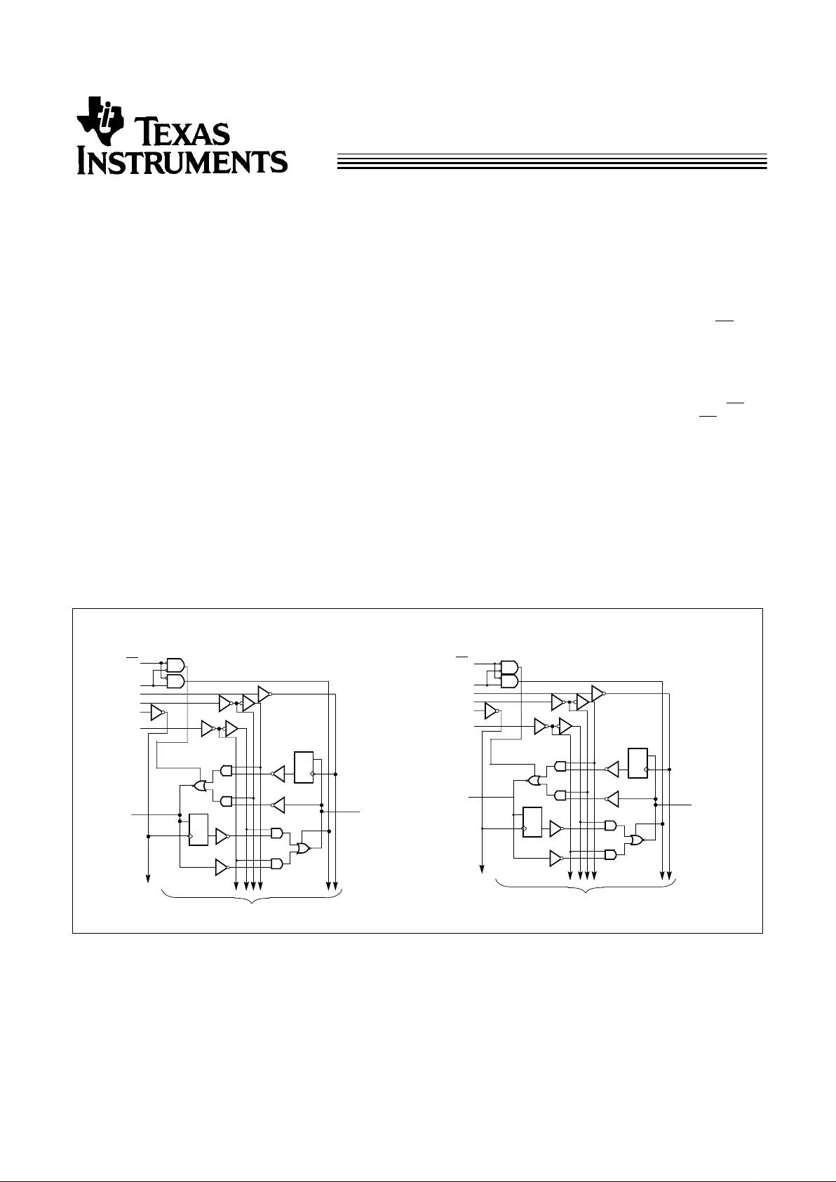
Functional Description
The CY74FCT16646T and CY74FCT162646T 16-bit
transceivers are three-state, D-type registers, and control
circuitry arranged for multiplexedtransmission of data directly
from the input bus or from the internal registers. Data on the A
or B bus will be clocked into the registers as the appropriate
clock pin goes to a HIGH logic level. Output Enable (
OE) and
direction pins (DIR) are provided to control the transceiver
function. In the transceiver mode, data present at the high
impedance port may be stored in either the A or B register, or
in both. The select controls can multiplex stored and real-time
(transparent mode) data. The direction control determines
which bus will receive data when the Output Enable (
OE) is
ActiveLOW.In the isolation mode (Output Enable(
OE)HIGH),
A data may be stored in the B register and/or B data may be
stored in the A register. The output buffers are designed with
a power-off disable feature that allows live insertion of boards.
The CY74FCT16646T is ideally suited for driving
high-capacitance loads and low-impedance backplanes.
The CY74FCT162646T has 24-mA balanced output drivers
with current limiting resistors in the outputs. This reduces the
need for external terminating resistors and provides for
minimal undershoot and reduced ground bounce. The
CY74FCT162646T is ideal for driving transmission lines.
Logic Block Diagrams
FCT16646-1
C
D
1
B
1
C
D
1
A
1
TO7 OTHER CHANNELS
1
SAB
1
CLKAB
1
CLKBA
1
DIR
1
SBA
1
OE
B REG
A REG
C
D
2
B
1
C
D
2A1
2
SAB
2
CLKAB
2
CLKBA
2
DIR
2
SBA
2
OE
B REG
FCT16646-2
TO 7 OTHER CHANNELS
A REG
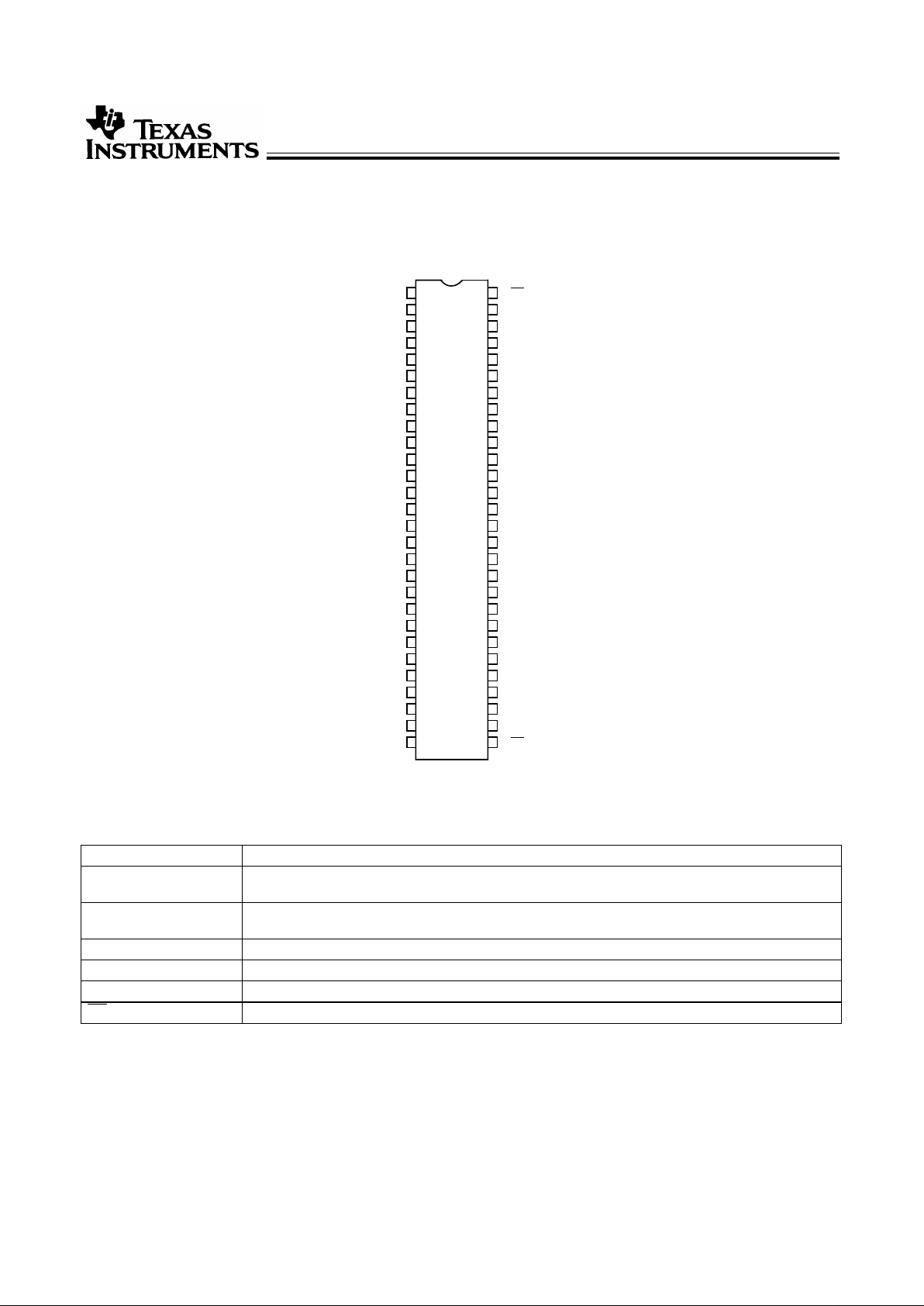
CY74FCT16646T
CY74FCT162646T
2
GND
1
DIR
SSOP/TSSOP
Top View
1
CLKAB
1
SAB
1A1
1A2
1
CLKBA
1
SBA
1B1
1
OE
GND
GND
V
CC
1A3
V
CC
GND
1A4
1A5
1A6
1A7
1A8
2A1
2A2
2A3
2A4
GND
2A5
2A6
V
CC
2A7
2A8
2
SAB
2
CLKAB
1
2
3
4
5
6
7
8
9
10
11
12
13
14
15
16
17
18
19
20
21
22
23
24
25
26
27
28
56
55
54
53
52
51
50
49
48
47
46
45
44
43
42
41
40
39
38
37
36
35
34
33
32
31
30
29
GND
2
DIR
1B2
1B3
1B4
1B5
1B6
1B7
1B8
2B1
2B2
2B3
GND
2B4
2B5
2B6
V
CC
2B7
2B8
GND
2
SBA
2
CLKBA
2
OE
FCT16646-3
Pin Configuration
Pin Description
Pin Names Description
A Data Register A Inputs
Data Register B Outputs
B Data Register B Inputs
Data Register A Outputs
CLKAB, CLKBA Clock Pulse Inputs
SAB, SBA Output Data Source Select Inputs
DIR Direction
OE Output Enable (Active LOW)

CY74FCT16646T
CY74FCT162646T
3
Function Table
[1]
Inputs Data I/O
[2]
Function
OE DIR CLKAB CLKBA SAB SBA A B
H
H
X
X
H or L H or L X
X
X
X
Input Input Isolation
Store A and B Data
L
L
L
L
X
X
X
H or L
X
X
LHOutput Input Real Time B Data to A Bus
Stored B Data to A Bus
L
L
H
H
X
H or L
X
X
L
H
X
X
Input Output Real Time A Data to Bus
Stored A Data to B Bus
Notes:
1. H = HIGH Voltage Level. L = LOW Voltage Level. X = Don’t Care
. = LOW-to-HIGH Transition
2. The data output functions may beenabledor disabled by various signals at the OE or DIR inputs. Data input functions arealways enabled, i.e., data at the
bus pins will be stored on every LOW-to-HIGH transition on the clock inputs.
3. Cannot transfer data to A-bus and B-bus simultaneously.
BUS BBUS A
DIRLOELCLKAB
X
SAB
X
BUS BBUS A
DIR
H
L
X
OE
L
L
H
CLKAB
X
SAB
X
X
X
SBA
X
X
X
BUS
BBUS A
DIRHOE
L
SAB
L
SBA
X
BUS ABUS A
DIR
L
H
OE
L
L
SAB
X
H
SBA
H
X
Real-Time Transfer
BusB to BusA
Real-TimeTransfer
BusA to BusB
Storagefrom
A and/or B
TransferStoredData
to A and/orB
CLKBA
X
CLKABXCLKBA
X
SBA
L
CLKBA
X
CLKAB
X
HorL
CLKBA
HorL
X
[3]
 Loading...