

Page 1
查询UC2823A供应商
High Speed PWM Controller
FEATURES
Improved versions of the
•
UC3823/UC3825 PWMs
Compatible with Voltage or
•
Current-Mode Topologies
Practical Operation at Switching
•
Frequencies to 1MHz
50ns Propagation Delay to Output
•
High Current Dual Totem Pole
•
Outputs (2A Peak)
Trimmed Oscillator Discharge Current
•
Low 100µA Startup Current
•
• Pulse-by-Pulse Current Limiting
Comparator
• Latched Overcurrent Comparator With
Full Cycle Restart
DESCRIPTION
The UC3823A & B and the UC3825A & B family of PWM control ICs are
improved versions of the standard UC3823 & UC3825 family. Performance
enhancements have been made to several of the circuit blocks. Error ampli
fier gain bandwidth product is 12MHz while input offset voltage is 2mV. Cur
rent limit threshold is guaranteed to a tolerance of 5%. Oscillator discharge
current is specified at 10mA for accurate dead time control. Frequency ac
curacy is improved to 6%. Startup supply current, typically 100µA, is ideal
for off-line applications. The output drivers are redesigned to actively sink
current during UVLO at no expense to the startup current specification. In
addition each output is capable of 2A peak currents during transitions.
Functional improvements have also been implemented in this family. The
UC3825 shutdown comparator is now a high-speed overcurrent comparator
with a threshold of 1.2V. The overcurrent comparator sets a latch that en
sures full discharge of the soft start capacitor before allowing a restart.
While the fault latch is set, the outputs are in the low state. In the event of
continuous faults, the soft start capacitor is fully charged before discharge
to insure that the fault frequency does not exceed the designed soft start
period. The UC3825 Clock pin has become CLK/LEB. This pin combines
the functions of clock output and leading edge blanking adjustment and has
been buffered for easier interfacing.
application
INFO
available
UC1823A,B/1825A,B
UC2823A,B/2825A,B
UC3823A,B/3825A,B
-
-
-
-
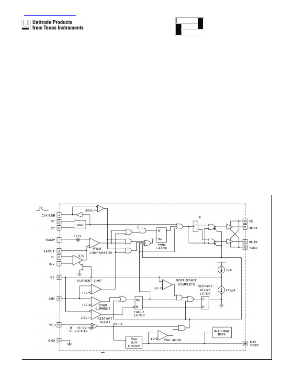
BLOCK DIAGRAM
(continued)
* Note: 1823A,B Version Toggles Q and Q are always low
SLUS334A - AUGUST 1995 - REVISED NOVEMBER 2000
UDG-95101
Page 2
DESCRIPTION (cont.)
The UC3825A,B has dual alternating outputs and the
same pin configuration of the UC3825. The UC3823A,B
outputs operate in phase with duty cycles from zero to
less than 100%. The pin configuration of the UC3823A,B
is the same as the UC3823 except pin 11 is now an out
put pin instead of the reference pin to the current limit
comparator. “A” version parts have UVLO thresholds
identical to the original UC3823/25. The “B” versions
have UVLO thresholds of 16 and 10V, intended for ease
of use in off-line applications.
Consult Application Note U-128 for detailed technical
and applications information. Contact the factory for fur
ther packaging and availability information.
Device UVLO Dmax
UC3823A 9.2V/8.4V < 100%
UC3823B 16V/10V < 100%
UC3825A 9.2V/8.4V < 50%
UC3825B 16V/10V < 50%
UC1823A,B/1825A,B
UC2823A,B/2825A,B
UC3823A,B/3825A,B
ABSOLUTE MAXIMUM RATINGS
Supply Voltage (VC, VCC) . . . . . . . . . . . . . . . . . . . . . . . . . 22V
Output Current, Source or Sink (Pins OUTA, OUTB)
DC . . . . . . . . . . . . . . . . . . . . . . . . . . . . . . . . . . . . . . . . . 0.5A
Pulse (0.5µs) . . . . . . . . . . . . . . . . . . . . . . . . . . . . . . . . . 2.2A
Power Ground (PGND). . . . . . . . . . . . . . . . . . . . . . . . . . . ±0.2V
-
Analog Inputs
(INV, NI, RAMP). . . . . . . . . . . . . . . . . . . . . . . . . –0.3V to 7V
(ILIM, SS). . . . . . . . . . . . . . . . . . . . . . . . . . . . . . –0.3V to 6V
Clock Output Current (CLK/LEB) . . . . . . . . . . . . . . . . . . . –5mA
Error Amplifier Output Current (EAOUT) . . . . . . . . . . . . . . 5mA
Soft Start Sink Current (SS) . . . . . . . . . . . . . . . . . . . . . . . 20mA
Oscillator Charging Current (RT) . . . . . . . . . . . . . . . . . . . –5mA
Power Dissipation at TA= 60°C . . . . . . . . . . . . . . . . . . . . . . 1W
Storage Temperature Range . . . . . . . . . . . . . –65°C to +150°C
-
Junction Temperature. . . . . . . . . . . . . . . . . . . –55°C to +150°C
Lead Temperature (Soldering, 10 sec.). . . . . . . . . . . . . . 300°C
All currents are positive into, negative out of the specified ter
minal. Consult Packaging Section of Databook for thermal limi
tations and considerations of packages.
-
-
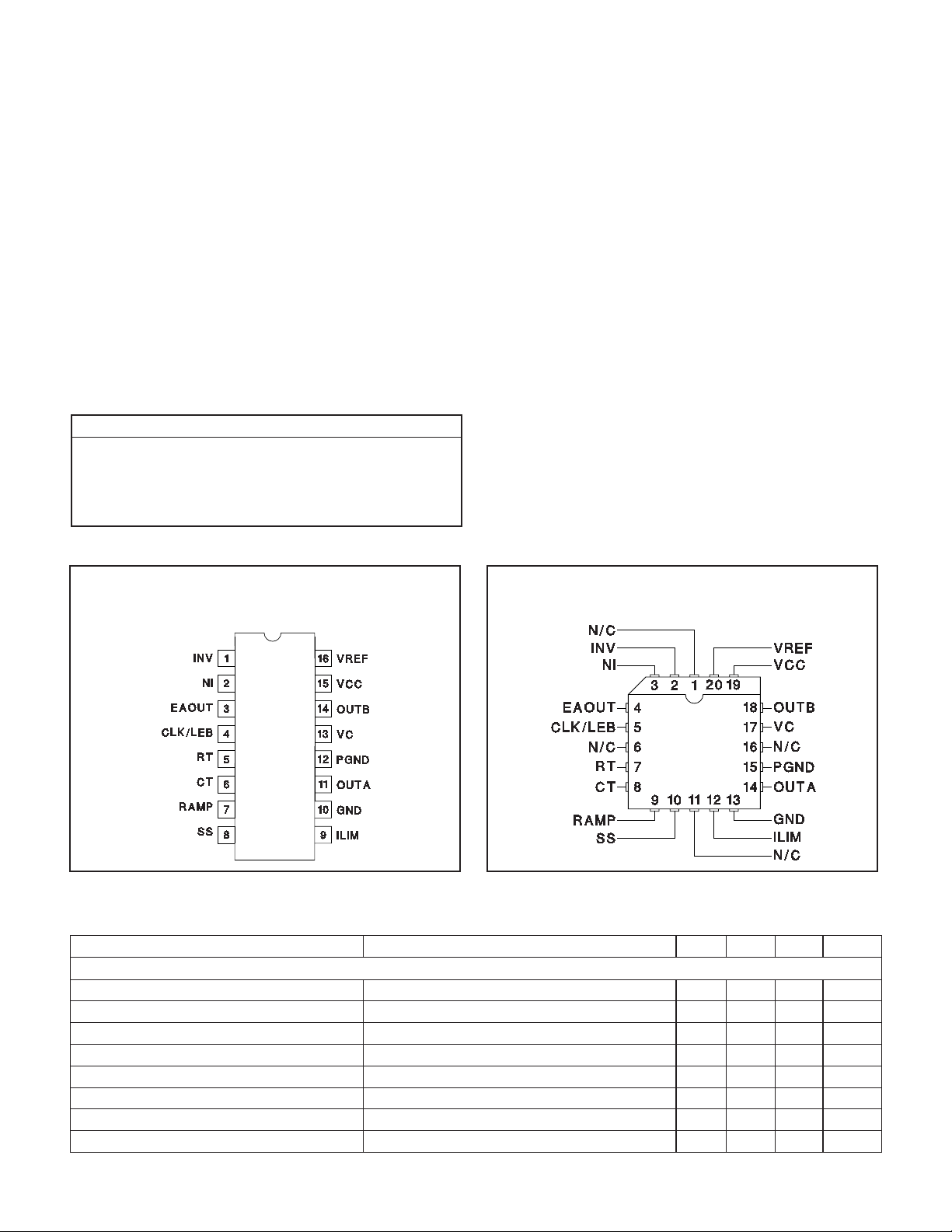
CONNECTION DIAGRAMS
DIL-16, SOIC-16, (Top View)
J or N Package;DW Package
ELECTRICAL CHARACTERISTICS:
the UC1823A,B and UC1825A,B; –40°C to +85°C for the UC2823A,B and UC2825A,B; 0°C to +70°C for the UC3823A,B and
UC3825A,B; RT = 3.65k, CT= 1nF, VCC = 12V, TA=T
PARAMETER TEST CONDITIONS MIN TYP MAX UNITS
Reference Section
Output Voltage T
Line Regulation 12 < VCC < 20V 2 15 mV
Load Regulation 1mA < I
Total Output Variation Line, Load, Temp 5.03 5.17 V
Temperature Stability T
Output Noise Voltage 10Hz < f < 10kHz (Note 1) 50 µVRMS
Long Term Stability T
Short Circuit Current VREF = 0V 30 60 90 mA
Unless otherwise stated, these specifications apply for TA= –55°C to +125°C for
J.
= 25°C, Io = 1mA 5.05 5.1 5.15 V
J
< 10mA 5 20 mV
O
< TA<T
MIN
= 125°C, 1000 hours (Note 1) 5 25 mV
J
MAX
PLCC-20, LCC-20, (Top View)
Q, L Packages
(Note 1) 0.2 0.4 mV/°C
2
Page 3
UC1823A,B/1825A,B
UC2823A,B/2825A,B
UC3823A,B/3825A,B
ELECTRICAL CHARACTERISTICS:
Unless otherwise stated, these specifications apply for TA= –55°C to +125°C for
the UC1823A,B and UC1825A,B; –40°C to +85°C for the UC2823A,B and UC2825A,B; 0°C to +70°C for the UC3823A,B and
UC3825A,B; RT = 3.65k, CT= 1nF, VCC = 12V, TA=T
J.
PARAMETER TEST CONDITIONS MIN TYP MAX UNITS
Oscillator Section
Initial Accuracy T
= 25°C (Note 1) 375 400 425 kHz
J
Total Variation Line, Temperature (Note 1) 350 450 kHz
Voltage Stability 12V < VCC < 20V 1 %
Temperature Stability T
MIN
< TA<T
Initial Accuracy RT= 6.6k, CT = 220pF, T
(Note 1) 5 %
MAX
= 25°C (Note 1) 0.9 1 1.1 MHz
A
Total Variation RT = 6.6k, CT = 220pF (Note 1) 0.85 1.15 MHz
Clock Out High 3.7 4 V
Clock Out Low 0 0.2 V
Ramp Peak 2.6 2.8 3 V
Ramp Valley 0.7 1 1.25 V
Ramp Valley to Peak 1.6 1.8 2 V
Oscillator Discharge Current RT = Open, V
= 2V 9 10 11 mA
CT
Error Amplifier Section
Input Offset Voltage 210mV
Input Bias Current 0.6 3 µA
Input Offset Current 0.1 1 µA
Open Loop Gain 1V < V
CMRR 1.5V < V
< 4V 60 95 dB
O
< 5.5V 75 95 dB
CM
PSRR 12V < VCC < 20V 85 110 dB
Output Sink Current V
Output Source Current V
Output High Voltage I
Output Low Voltage I
= 1V 1 2.5 mA
EAOUT
= 4V –0.5 –1.3 mA
EAOUT
= –0.5mA 4.5 4.7 5 V
EAOUT
= 1mA 0 0.5 1 V
EAOUT
Gain Bandwidth Product F = 200kHz 6 12 MHz
Slew Rate (Note 1) 6 9 V/µs
PWM Comparator
RAMP Bias Current V
= 0V –1 –8 µA
RAMP
Minimum Duty Cycle 0%
Maximum Duty Cycle 85 %
Leading Edge Blanking R = 2k, C = 470pF 300 375 450 ns
LEB Resistor V
EAOUT Zero D.C. Threshold V
Delay to Output V
CLK/LEB
RAMP
EAOUT
= 3V 8.5 10 11.5 kohm
= 0V 1.1 1.25 1.4 V
= 2.1V, V
= 0 to 2V Step (Note 1) 50 80 ns
RAMP
Current Limit/Start Sequence/Fault Section
Soft Start Charge Current VSS= 2.5V 8 14 20 µA
Full Soft Start Threshold 4.3 5 V
Restart Discharge Current V
= 2.5V 100 250 350 µA
SS
Restart Threshold 0.3 0.5 V
ILIM Bias Current 0 < V
< 2V 15 µA
ILIM
Current Limit Threshold 0.95 1 1.05 V
3
Page 4

UC1823A,B/1825A,B
UC2823A,B/2825A,B
UC3823A,B/3825A,B
ELECTRICAL CHARACTERISTICS:
the UC1823A,B and UC1825A,B; –40°C to +85°C for the UC2823A,B and UC2825A,B; 0°C to +70°C for the UC3823A,B and
UC3825A,B; RT = 3.65k, CT= 1nF, VCC = 12V, TA=T
PARAMETER TEST CONDITIONS MIN TYP MAX UNITS
Current Limit/Start Sequence/Fault Section (cont.)
Over Current Threshold 1.14 1.2 1.26 V
ILIM Delay to Output V
Output Section
Output Low Saturation I
Output High Saturation I
UVLO Output Low Saturation I
Rise/Fall Time C
UnderVoltage Lockout
Start Threshold UCX823B and X825B only 16 17 V
Stop Threshold UCX823B and X825B only 9 10 V
UVLO Hysteresis UCX823B and X825B only 5 6 7 V
Start Threshold UCX823A and X825A only 8.4 9.2 9.6 V
UVLO Hysteresis UCX823A and X825A only 0.4 0.8 1.2 V
Supply Current
Startup Current VC = VCC = V
Icc 28 36 mA
Unless otherwise stated, these specifications apply for TA= –55°C to +125°C for
J.
= 0 to 2V Step (Note 1) 50 80 ns
ILIM
= 20mA 0.25 0.4 V
OUT
= 200mA 1.2 2.2 V
I
OUT
= 20mA 1.9 2.9 V
OUT
= 200mA 2 3 V
I
OUT
= 20mA 0.8 1.2 V
O
= 1nF (Note 1) 20 45 ns
L
(start) –0.5V 100 300 µA
TH
Note 1:Guaranteed by design.Not 100% tested in production.
APPLICATIONS INFORMATION
OSCILLATOR
The UC3823A,B/3825A,B oscillator is a saw tooth. The
rising edge is governed by a current controlled by the RT
pin and value of capacitance at the CT pin. The falling
edge of the sawtooth sets dead time for the outputs. Se
lection of RT should be done first, based on desired
maximum duty cycle. CT can then be chosen based on
desired frequency, RT, and D
are:
V
RT
=
()
10 1–
()
CT
=
3
mA D
()
MAX
D
••16.
MAX
()
RT F
Recommended values for RT range from 1k to 100k.
Control of D
less than 70% is not recommended.
MAX
. The design equations
MAX
Oscillator
-
UDG-95102
4
Page 5

APPLICATIONS INFORMATION (cont.)
OSCILLATOR (cont.)
UC1823A,B/1825A,B
UC2823A,B/2825A,B
UC3823A,B/3825A,B
Oscillator Frequency vs. RTand CTCurve
UDG-95103
LEADING EDGE BLANKING
The UC3823A,B/3825A,B performs fixed frequency
pulse width modulation control. The UC3823A,B outputs operate together at the switching frequency and
can vary from 0 to some value less than 100%. The
UC3825A,B outputs are alternately controlled. During
every other cycle, one output will be off. Each output
then, switches at one-half the oscillator frequency, varying in duty cycle from 0 to less than 50%.
Maximum Duty Cycle vs RTCurve
UDG-95104
LEB Operational Waveforms
To limit maximum duty cycle, the internal clock pulse
blanks both outputs low during the discharge time of
the oscillator. On the falling edge of the clock, the ap
propriate output(s) is driven high. The end of the pulse
is controlled by the PWM comparator, current limit com
parator, or the overcurrent comparator.
Normally the PWM comparator will sense a ramp
crossing a control voltage (error amp output) and termi
nate the pulse. Leading edge blanking (LEB) causes
the PWM comparator to be ignored for a fixed amount
of time after the start of the pulse. This allows noise in
herent with switched mode power conversion to be re
jected. The PWM ramp input may not require any
filtering as result of leading edge blanking.
To program a Leading Edge Blanking period, connect a
capacitor, C, to CLK/LEB. The discharge time set by C
and the internal 10k resistor will determine the blanked
interval. The 10k resistor has a 10% tolerance. For
more accuracy, an external 2k 1% resistor, R, can be
added, resulting in an equivalent resistance of 1.66k
with a tolerance of 2.4%.The design equation is:
-
-
-
= 0.5 • (R | | 10k) • C.
-
-
t
LEB
Values of R less than 2k should not be used
Leading edge blanking is also applied to the current
limit comparator. After LEB, if the ILIM pin exceeds the
one volt threshold, the pulse is terminated. The over
current comparator, however, is not blanked. It will
catch catastrophic over current faults without a blanking
delay. Any time the ILIM pin exceeds 1.2V, the fault
latch will be set and the outputs driven low. For this rea
son, some noise filtering may be required on the ILIM
pin.
UDG-95105
-
5
Page 6

APPLICATIONS INFORMATION (cont.)
UC1823A,B/1825A,B
UC2823A,B/2825A,B
UC3823A,B/3825A,B
UVLO,SOFT START AND FAULT MANAGEMENT
Soft start is programmed by a capacitor on the SS pin. At
power up, SS is discharged. When SS is low, the error
amp output is also forced low. As the internal 9µA source
charges the SS pin, the error amp output follows until
closed loop regulation takes over.
Anytime ILIM exceeds 1.2V, the fault latch will be set and
the output pins will be driven low. The soft start cap is
then discharged by a 250µA current sink. No more output
pulses are allowed until soft start is fully discharged, and
ILIM is below 1.2V. At this point the fault latch will be re
set and the chip will execute a soft start.
Should the fault latch be set during soft start, the outputs
will be immediately terminated, but the soft start cap will
not be discharged until it has been fully charged. This re-
ACTIVE LOW OUTPUTS DURING UVLO
The UVLO function forces the outputs to be low and considers both VCC and VREF before allowing the chip to
operate.
Soft Start and Fault Waveforms
-
UDG-95106
sults in a controlled hiccup interval for continuous
fault conditions.
Output V and I During UVLO
Simplified Schematic
PWM APPLICATIONS
Current Mode
UDG-95108
UDG-95107
Voltage Mode
UDG-95110UDG-95109
6
Page 7

APPLICATIONS INFORMATION (cont.)
UC1823A,B/1825A,B
UC2823A,B/2825A,B
UC3823A,B/3825A,B
SYNCHRONIZATION
The oscillator can be synchronized by an external pulse
inserted in series with the timing capacitor. Program the
free running frequency of the oscillator to be 10 to 15%
slower than the desired synchronous frequency.The
pulse width should be greater than 10ns and less than
half the discharge time of the oscillator.The rising edge of
the CLK/LEB pin can be used to generate a synchroniz
ing pulse for other chips.Note that, the CLK/LEB pin will
no longer accept an incoming synchronizing signal.
General Oscillator Synchronization
UDG-95111
Operational Waveforms
-
UDG-95112
Two Units
UDG-95113
HIGH CURRENT OUTPUTS
Each totem pole output of the UC3823A,B and
UC3825A,B can deliver a 2 amp peak current into a capacitive load. The output can slew a 1000pF capacitor 15
volts in approximately 20 nanoseconds. Separate collec
tor supply (VC) and power ground (PGND) pins help de
couple the IC's analog circuitry from the high power gate
drive noise. The use of 3 Amp Schottky diodes (1N5120,
USD245 or equivalent) as shown in the figure from each
output to both VC and PGND are recommended. The di
odes clamp the output swing to the supply rails, neces
sary with any type of inductive/capacitive load, typical of a
MOSFET gate. Schottky diodes must be used because a
low forward voltage drop is required. DO NOT USE stan
dard silicon diodes.
Although a "single ended" device, two output drivers are
available on the UC3823A,B devices. These can be “par
alleled” by the use of a one-half ohm (noninductive) resis
tor connected in series with each output for a combined
peak current of 4 amps.
Power MOSFET Drive Circuit
-
-
-
-
-
-
-
UDG-95114
7
Page 8

APPLICATIONS INFORMATION (cont.)
GROUND PLANES
UC1823A,B/1825A,B
UC2823A,B/2825A,B
UC3823A,B/3825A,B
Each output driver of these devices is capable of 2A
peak currents. Careful layout is essential for correct op
eration of the chip. A ground plane must be employed.
A unique section of the ground plane must be desig
nated for high di/dt currents associated with the output
stages. This point is the power ground to which the
PGND pin is connected. Power ground can be sepa
rated from the rest of the ground plane and connected
at a single point, although this is not strictly necessary
if the high di/dt paths are well understood and ac
counted for. VCC should be bypassed directly to power
ground with a good high frequency capacitor. The
sources of the power MOSFET should connect to
power ground as should the return connection for input
power to the system and the bulk input capacitor. The
output should be clamped with a high current Schottky
diode to both VCC and PGND. Nothing else should be
connected to power ground.
-
VREF should be bypassed directly to the signal portion
of the ground plane with a good high frequency capaci
tor. Low ESR/ESL ceramic 1µF capacitors are recom
-
mended for both VCC and VREF. All analog circuitry
should likewise be bypassed to the signal ground
plane.
-
-
Open Loop Test Circuit
This test fixture is useful for exercising many of the
UC3823A,B, UC3825A,B functions and measuring their
specifications. As with any wideband circuit, careful
UDG-95115
grounding and bypass procedures should be followed.
The use of a ground plane is highly recommended.
UNITRODE CORPORATION
7 CONTINENTAL BLVD.• MERRIMACK, NH 03054
TEL. (603) 424-2410 • FAX (603) 424-3460
UDG-95116
8
Page 9

IMPORTANT NOTICE
T exas Instruments and its subsidiaries (TI) reserve the right to make changes to their products or to discontinue
any product or service without notice, and advise customers to obtain the latest version of relevant information
to verify, before placing orders, that information being relied on is current and complete. All products are sold
subject to the terms and conditions of sale supplied at the time of order acknowledgment, including those
pertaining to warranty, patent infringement, and limitation of liability.
TI warrants performance of its semiconductor products to the specifications applicable at the time of sale in
accordance with TI’s standard warranty. T esting and other quality control techniques are utilized to the extent
TI deems necessary to support this warranty . Specific testing of all parameters of each device is not necessarily
performed, except those mandated by government requirements.
Customers are responsible for their applications using TI components.
In order to minimize risks associated with the customer’s applications, adequate design and operating
safeguards must be provided by the customer to minimize inherent or procedural hazards.
TI assumes no liability for applications assistance or customer product design. TI does not warrant or represent
that any license, either express or implied, is granted under any patent right, copyright, mask work right, or other
intellectual property right of TI covering or relating to any combination, machine, or process in which such
semiconductor products or services might be or are used. TI’s publication of information regarding any third
party’s products or services does not constitute TI’s approval, warranty or endorsement thereof.
Copyright 2000, Texas Instruments Incorporated
 Loading...