

Page 1

L M K 0 4 9 0 6 E V A L U A T I O N B O A R D O P E R A T I N G I N S T R U C T I O N S
1
LMK04906 Family
Low-Noise Clock Jitter Cleaner with Dual Loop PLLs
LMK04906 Evaluation Board Operating Instructions
Texas Instruments
June 2012
SNAU126
Page 2

L M K 0 4 9 0 6 E V A L U A T I O N B O A R D O P E R A T I N G I N S T R U C T I O N S
2
Table of Contents
TABLE OF CONTENTS .............................................................................................................................................. 2
GENERAL DESCRIPTION .......................................................................................................................................... 4
EVALUATION BOARD KIT CONTENTS .................................................................................................................................. 4
AVAILABLE LMK04906 EVALUATION BOARDS .................................................................................................................... 4
AVAILABLE LMK04906 FAMILY DEVICES ........................................................................................................................... 4
QUICK START ......................................................................................................................................................... 5
DEFAULT CODELOADER MODES FOR EVALUATION BOARDS .................................................................................................... 6
EXAMPLE: USING CODELOADER TO PROGRAM THE LMK04906B ........................................................................... 7
1. START CODELOADER 4 APPLICATION.............................................................................................................................. 7
2. SELECT DEVICE .......................................................................................................................................................... 7
3. PROGRAM/LOAD DEVICE ............................................................................................................................................. 8
4. RESTORING A DEFAULT MODE ...................................................................................................................................... 8
5. VISUAL CONFIRMATION OF FREQUENCY LOCK .................................................................................................................. 9
6. ENABLE CLOCK OUTPUTS ............................................................................................................................................. 9
PLL LOOP FILTERS AND LOOP PARAMETERS......................................................................................................... 11
PLL 1 LOOP FILTER ...................................................................................................................................................... 11
122.88 MHz VCXO PLL ........................................................................................................................................ 11
PLL2 LOOP FILTER ....................................................................................................................................................... 12
EVALUATION BOARD INPUTS AND OUTPUTS ....................................................................................................... 13
RECOMMENDED TEST EQUIPMENT...................................................................................................................... 20
PROGRAMMING 0-DELAY MODE IN CODELOADER .............................................................................................. 21
OVERVIEW.................................................................................................................................................................. 21
DUAL LOOP 0-DELAY MODE EXAMPLES ........................................................................................................................... 21
Programming Steps ............................................................................................................................................ 21
Details ................................................................................................................................................................ 21
SINGLE LOOP 0-DELAY MODE EXAMPLES ......................................................................................................................... 23
Programming Steps ............................................................................................................................................ 23
Details ................................................................................................................................................................ 23
APPENDIX A: CODELOADER USAGE ...................................................................................................................... 25
PORT SETUP TAB ......................................................................................................................................................... 25
CLOCK OUTPUTS TAB ................................................................................................................................................... 26
PLL1 TAB ................................................................................................................................................................... 28
Setting the PLL1 VCO Frequency and PLL2 Reference Frequency ....................................................................... 29
PLL2 TAB ................................................................................................................................................................... 30
BITS/PINS TAB ............................................................................................................................................................ 31
REGISTERS TAB ............................................................................................................................................................ 36
APPENDIX B: TYPICAL PHASE NOISE PERFORMANCE PLOTS ................................................................................. 37
PLL1 ......................................................................................................................................................................... 37
122.88 MHz VCXO Phase Noise .......................................................................................................................... 37
Clock Output Measurement Technique .............................................................................................................. 38
Buffered OSCout Phase Noise............................................................................................................................. 38
CLOCK OUTPUTS (CLKOUT) ........................................................................................................................................... 39
SNAU126
Page 3

L M K 0 4 9 0 6 E V A L U A T I O N B O A R D O P E R A T I N G I N S T R U C T I O N S
3
LMK04906B CLKout Phase Noise ........................................................................................................................ 39
LMK04906B OSCout Phase Noise ....................................................................................................................... 41
APPENDIX C: SCHEMATICS ................................................................................................................................... 42
POWER SUPPLIES ......................................................................................................................................................... 42
LMK04906B DEVICE WITH LOOP FILTER AND CRYSTAL CIRCUITS ......................................................................................... 43
REFERENCE INPUTS (CLKIN0, CLKIN1 & CLKIN2), EXTERNAL VCXO (OSCIN) & VCO CIRCUITS ................................................ 44
CLOCK OUTPUTS (OSCOUT0, CLKOUT0 TO CLKOUT5) ...................................................................................................... 45
UWIRE HEADER, LOGIC I/O PORTS AND STATUS LEDS........................................................................................................ 46
APPENDIX D: BILL OF MATERIALS ........................................................................................................................ 47
APPENDIX E: PCB LAYERS STACKUP ..................................................................................................................... 52
APPENDIX F: PCB LAYOUT .................................................................................................................................... 53
LAYER #1 – TOP .......................................................................................................................................................... 53
LAYER #2 – RF GROUND PLANE (INVERTED) ..................................................................................................................... 54
LAYER #3 – VCC PLANES ............................................................................................................................................... 55
LAYER #4 – GROUND PLANE (INVERTED) .......................................................................................................................... 56
LAYER # 5 – VCC PLANES 2 ............................................................................................................................................ 57
LAYER #6 – BOTTOM .................................................................................................................................................... 58
LAYERS #1 AND 6 – TOP AND BOTTOM (COMPOSITE) ......................................................................................................... 59
APPENDIX G: PROPERLY CONFIGURING LPT PORT ............................................................................................... 60
LPT DRIVER LOADING ................................................................................................................................................... 60
CORRECT LPT PORT/ADDRESS ....................................................................................................................................... 60
CORRECT LPT MODE .................................................................................................................................................... 61
APPENDIX H: TROUBLESHOOTING INFORMATION ............................................................................................... 62
1) CONFIRM COMMUNICATIONS ............................................................................................................................... 62
2) CONFIRM PLL1 OPERATION/LOCKING .................................................................................................................... 62
3) CONFIRM PLL2 OPERATION/LOCKING .................................................................................................................... 63
SNAU126
Page 4

L M K 0 4 9 0 6 E V A L U A T I O N B O A R D O P E R A T I N G I N S T R U C T I O N S
4
Evaluation Board ID
Device
PLL1 VCXO
LMK04906BEVAL
LMK04906B
122.88 MHz Crystek VCXO
Model CVHD-950-122.880
Device
Reference
Inputs
Buffered/
Divided
OSCin
Outputs
Programmable
LVDS/LVPECL/
LVCMOS
Outputs
VCO Frequency
LMK04906B
3 1 6
2370 to 2600 MHz
General Description
The LMK04906 Evaluation Board simplifies evaluation of the LMK04906B Low-Noise Clock
Jitter Cleaner with Dual Loop PLLs. Texas Instrument‟s CodeLoader software can be used to
program the internal registers of the LMK04906B device through the MICROWIRETM interface.
The CodeLoader software will run on a Windows 2000 or Windows XP PC and can be
downloaded from http://www.ti.com/codeloader.
Evaluation Board Kit Contents
The evaluation board kit includes:
(1) LMK04906 Evaluation Board from Table 1
(1) CodeLoader uWire cable (LPT uWire)
Available LMK04906 Evaluation Boards
The LMK04906 Evaluation Board supports any of the four devices offered in the LMK04906
Family. All evaluation boards use the same PCB layout and bill-of-materials, except for the
corresponding LMK04906B device affixed to the board. A commercial-quality VCXO is also
mounted to the board to provide a known reference point for evaluating device performance and
functionality.
Table 1: Available Evaluation Board Configurations
Available LMK04906 Family Devices
Table 2: LMK04906B Devices
SNAU126
Page 5

L M K 0 4 9 0 6 E V A L U A T I O N B O A R D O P E R A T I N G I N S T R U C T I O N S
5
CLKout
0
CLKout
0
*
Laptop or PC
Parallel Port
Connector
5.0 V
(LDO)
1
3
4
Program with CodeLoader
Be sure to press ‘Ctrl - L’
CLKin
1
Reference clock from
signal generator or other
external source.
122.88 MHz
(Default)
2
Power
Reference
LMK04906
uWire
header
CLKout1
CLKout1*
CLKout
2
*
CLKout
2
CLKout
3
*
CLKout
3
CLKout
4
CLKout
4
*
CLKout
5
*
CLKout
5
OSCout0
OSCout0*
CLKin
0
CLKin
0
*
5.0 V
3.3 V
Factory default is LDO is used.
Customer may reconfigure to
power LMK directly.
OSCin
OSCin*
CLKin
2
CLKin
2
*
Parallel Port Ribbon
Cable
Quick Start
Full evaluation board instructions are downloadable from the LMK04906B device product folder
at www.ti.com.
1. Connect a power supply voltage of 5 V to the Vcc SMA connector. The onboard
LP3878-ADJ LDO regulator will output a low-noise 3.3 V supply to operate the device.
2. Connect a reference clock from a signal source to the CLKin1 SMA port. Use 122.88
MHz for default. The reference frequency depends on the device programming.
3. Connect the uWire header to a PC parallel port using the CodeLoader cable. A USB
interface is also available (search for “USB2UWIRE-IFACE” at www.ti.com).
4. Program the device with a default mode using CodeLoader. Ctrl+L must be pressed at
least once to load all registers. Alternatively click menu “Keyboard Controls” “Load
Device”. CodeLoader can be downloaded from www.ti.com/tool/codeloader/.
5. Measurements may be made on an active output clock port via its SMA connector.
Figure 1: Quick Start Diagram
SNAU126
Page 6

L M K 0 4 9 0 6 E V A L U A T I O N B O A R D O P E R A T I N G I N S T R U C T I O N S
6
Default CodeLoader Mode
Device Mode
CLKin
Frequency
OSCin
Frequency
122.88 MHz CLKin1, 122.88 MHz
VCXO
Dual PLL, Internal VCO
122.88 MHz
122.88 MHz
122.88 MHz CLKin1, Dual Loop 0delay, 122.88 MHz VCXO
Dual PLL, Internal VCO,
0-Delay with Internal
Feedback
122.88 MHz
122.88 MHz
122.88 MHz CLKin1, 122.88 MHz
VCXO
Dual PLL, Internal VCO,
PLL2 Crystal Oscillator
Enabled
122.88 MHz
20.48 MHz
122.88 MHz CLKin1, 122.88 MHz
VCXO
Dual PLL, Internal VCO
122.88 MHz
122.88 MHz
122.88 MHz CLKin1, Dual Loop 0delay, 122.88 MHz VCXO
Dual PLL, Internal VCO,
0-Delay with Internal
Feedback
122.88 MHz
122.88 MHz
122.88 MHz CLKin1, 122.88 MHz
VCXO
Dual PLL, Internal VCO,
PLL2 Crystal Oscillator
Enabled
122.88 MHz
20.48 MHz
Default CodeLoader Modes for Evaluation Boards
CodeLoader saves the state of the selected LMK04906B device when exiting the software. To
ensure a common starting point, the following modes listed in Table 3 may be restored by
clicking “Mode” and selecting the appropriate device configuration, as shown in Figure 2 in the
case of the LMK04906B device. Similar default modes are available for each LMK04906B
device in CodeLoader. Choose a mode with CLKin0 or CLKin2 for differential clock signal or
CLKin1 for a single ended signal.
Figure 2: Selecting a Default Mode for the LMK04906 Device
After restoring a default mode, press Ctrl+L to program the device. The default modes also
disable certain outputs, so make sure to enable the output under test to make measurements.
Table 3: Default CodeLoader Modes for LMK04906
The next section outlines step-by-step procedures for using the evaluation board with the
LMK04906B. For boards with another part number, make sure to select the corresponding part
number under the “Device” menu.
SNAU126
Page 7

L M K 0 4 9 0 6 E V A L U A T I O N B O A R D O P E R A T I N G I N S T R U C T I O N S
7
Figure 3 – Selecting the LMK04906B device
Example: Using CodeLoader to Program the LMK04906B
The purpose of this section is to walk the user through using CodeLoader 4 to make some
measurements with the LMK04906B device as an example. For more information on
CodeLoader refer to Appendix A: CodeLoader Usage or the CodeLoader 4 instructions located
at http://www.ti.com/tool/codeloader.
Before proceeding, be sure to follow the Quick Start section above to ensure proper connections.
1. Start CodeLoader 4 Application
Click “Start” “Programs” “CodeLoader 4” “CodeLoader 4”
The CodeLoader 4 program is installed by default to the CodeLoader 4 application group.
2. Select Device
Click “Select Device” “Clock
Conditioners” “LMK04906B”
Once started CodeLoader 4 will load the last
used device. To load a new device click
“Select Device” from the menu bar, then
select the subgroup and finally device to
load. For this example, the LMK04906B is
chosen. Selecting the device does cause the
device to be programmed.
SNAU126
Page 8

L M K 0 4 9 0 6 E V A L U A T I O N B O A R D O P E R A T I N G I N S T R U C T I O N S
8
Figure 4 – Loading the Device
3. Program/Load Device
Assuming the Port Setup settings are correct,
press the “Ctrl+L” shortcut or click “Keyboard
Controls” “Load Device” from the menu to
program the device to the current state of the
newly loaded LMK04906 file.
Once the device has been initially loaded,
CodeLoader will automatically program changed
registers so it is not necessary to re-load the device upon subsequent changes in the device
configuration. It is possible to disable this functionality by ensuring there is no checkmark by
the “Options” “AutoReload with Changes.”
Because a default mode will be restored in the next step, this step isn‟t really needed but included
to emphasize the importance of pressing “Ctrl+L” to load the device at least once after starting
CodeLoader, restoring a mode, or restoring a saved setup using the File menu.
See Appendix A: CodeLoader Usage or the CodeLoader 4 instructions located at
http://www.ti.com/tool/codeloader for more information on Port Setup. Appendix H:
Troubleshooting Information contains information on troubleshooting communications.
4. Restoring a Default Mode
Click “Mode” “LMK04906B, 122.88 MHz VCXO, 122.88 MHz CLKin1”; then press Ctrl+L.
Figure 5: Setting the Default mode for LMK04906
For the purpose of this walkthrough, a default mode will be loaded to ensure a common starting
point. This is important because when CodeLoader is closed, it remembers the last settings used
for a particular device. Again, remember to press Ctrl+L as the first step after loading a default
mode.
SNAU126
Page 9

L M K 0 4 9 0 6 E V A L U A T I O N B O A R D O P E R A T I N G I N S T R U C T I O N S
9
Figure 7: Setting LVCMOS modes
Figure 6: Setting Digital Delay, Clock Divider, Analog Delay, and Output Format for CLKout0
5. Visual Confirmation of Frequency Lock
After a default mode is restored and loaded, LED D5 should illuminate when PLL1 and PLL2
are locked to the reference clock applied to CLKin1. This assumes LD_MUX = PLL1/2 DLD
and LD_TYPE = Active High, which are the default settings.
6. Enable Clock Outputs
While the LMK04906B offers programmable clock output buffer formats, the evaluation board
is shipped with preconfigured output terminations to match the default buffer type for each
output. Refer to the CLKout port description in the Evaluation Board Inputs and Outputs section.
To measure phase noise at one of the clock outputs, for example, CLKout0:
1. Click on the Clock Outputs tab,
2. Uncheck “Powerdown” in the Digital Delay box to enable the channel,
3. Set the following settings as needed:
a. Digital Delay value
b. Clock Divider value
c. Analog Delay select and Analog Delay value (if not “Bypassed”)
d. Clock Output type.
4. Depending on the configured output type, the clock output SMAs can be interfaced to a
test instrument with a single-ended 50-ohm input as follows.
a. For LVDS:
i. A balun (like ADT2-1T) is recommended for differential-to-single-ended
conversion.
b. For LVPECL:
i. A balun can be used, or
ii. One side of the LVPECL signal can be terminated with a 50-ohm load and
the other side can be run single-ended to the instrument.
c. For LVCMOS:
i. There are two single-ended outputs,
CLKoutX and CLKoutX*, and each
output can be set to Normal, Inverted, or
Off. There are nine (9) combinations of
LVCMOS modes in the Clock Output list.
ii. One side of the LVCMOS signal can be
terminated with a 50-ohm load and the
other side can be run single-ended to the
instrument.
iii. A balun may also be used. Ensure
CLKoutX and CLKoutX* states are
complementary to each other, i.e.:
SNAU126
Page 10

L M K 0 4 9 0 6 E V A L U A T I O N B O A R D O P E R A T I N G I N S T R U C T I O N S
10
Norm/Inv or Inv/Norm.
5. The phase noise may be measured with a spectrum analyzer or signal source analyzer.
See Appendix B: Typical Phase Noise Performance Plots for phase noise plots of the clock
outputs.
TI‟s Clock Design Tool can be used to calculate divider values to achieve desired clock output
frequencies. See: http://www.ti.com/tool/codeloader.
SNAU126
Page 11

L M K 0 4 9 0 6 E V A L U A T I O N B O A R D O P E R A T I N G I N S T R U C T I O N S
11
122.88 MHz VCXO PLL
Phase Margin
49˚
Kφ (Charge Pump)
100 uA
Loop Bandwidth
12 Hz
Phase Detector Freq
1.024 MHz
VCO Gain
2.5 kHz/Volt
Reference Clock
Frequency
122.88 MHz
Output Frequency
122.88 MHz (To PLL 2)
Loop Filter
Components
C1_A1 = 100 nF
C2_A1 = 680 nF
R2_A1 = 39 kΩ
PLL Loop Filters and Loop Parameters
In jitter cleaning applications that use a cascaded or dual PLL architecture, the first PLL‟s
purpose is to substitute the phase noise of a low-noise oscillator (VCXO or crystal resonator) for
the phase noise of a “dirty” reference clock. The first PLL is typically configured with a narrow
loop bandwidth in order to minimize the impact of the reference clock phase noise. The reference
clock consequently serves only as a frequency reference rather than a phase reference.
The loop filters on the LMK04906 evaluation board are setup using the approach above. The
loop filter for PLL1 has been configured for a narrow loop bandwidth (< 100 Hz), while the loop
filter of PLL2 has been configured for a wide loop bandwidth (> 100 kHz). The specific loop
bandwidth values depend on the phase noise performance of the oscillator mounted on the board.
The following tables contain the parameters for PLL1 and PLL2 for each oscillator option.
TI‟s Clock Design Tool can be used to optimize PLL phase noise/jitter for given specifications.
See: http://www.ti.com/tool/codeloader.
PLL 1 Loop Filter
Table 4: PLL1 Loop Filter Parameters for Crystek 122.88 MHz VCXO
Note: PLL Loop Bandwidth is a function of K , Kvco, N as well as loop components. Changing
K and N will change the loop bandwidth.
SNAU126
Page 12

L M K 0 4 9 0 6 E V A L U A T I O N B O A R D O P E R A T I N G I N S T R U C T I O N S
12
LMK04906B
C1_A2
0.047
nF
C2_A2
3.9
nF
C3 (internal)
0
nF
C4 (internal)
0
nF
R2_A2
0.62
kΩ
R3 (internal)
0.2
kΩ
R4 (internal)
0.2
kΩ
Charge Pump
Current, K
3.2
mA
Phase Detector
Frequency
122.88
MHz
Frequency
2457.6
MHz
Kvco
18.8
MHz/V N 20
Phase Margin
75
degrees
Loop
Bandwidth
321
kHz
PLL2 Loop Filter
Table 5: PLL2 Loop Filter Parameters for LMK04906B
Note: PLL Loop Bandwidth is a function of K , Kvco, N as well as loop components. Changing
K and N will change the loop bandwidth.
SNAU126
Page 13

L M K 0 4 9 0 6 E V A L U A T I O N B O A R D O P E R A T I N G I N S T R U C T I O N S
13
Connector Name
Signal Type,
Input/Output
Description
Populated:
CLKout0, CLKout0*,
CLKout1, CLKout1*,
CLKout2, CLKout2*,
CLKout3, CLKout3*,
CLKout4, CLKout4*,
CLKout5, CLKout5*
Analog,
Output
Clock outputs with programmable output buffers.
The output terminations by default on the evaluation
board are shown below, and the output type selected by
default in CodeLoader is indicated by an asterisk (*):
Clock output pair
Default Board
Termination
CLKout0
LVPECL*
CLKout1
LVPECL
CLKout2
LVDS* / LVCMOS
CLKout3
LVDS / LVCMOS
CLKout4
LVDS* / LVCMOS
CLKout5
LVPECL
Each CLKout pair has a programmable LVDS,
LVPECL, or LVCMOS buffer. The output buffer type
can be selected in CodeLoader in the Clock Outputs
tab via the CLKoutX_TYPE control.
All clock outputs are AC-coupled to allow safe testing
with RF test equipment.
All LVPECL clock outputs are source-terminated using
240-ohm resistors.
If an output pair is programmed to LVCMOS, each
output can be independently configured (normal,
inverted, or off/tri-state).
Evaluation Board Inputs and Outputs
The following table contains descriptions of the inputs and outputs for the evaluation board.
Unless otherwise noted, the connectors described can be assumed to be populated by default.
Additionally, some applicable CodeLoader programming controls are noted for convenience.
Refer to the LMK04906 Family Datasheet for complete register programming information.
Table 6: Evaluation Board Inputs and Outputs
SNAU126
Page 14

L M K 0 4 9 0 6 E V A L U A T I O N B O A R D O P E R A T I N G I N S T R U C T I O N S
14
Connector Name
Signal Type,
Input/Output
Description
Populated:
OSCout0, OSCout0*,
Analog,
Output
Buffered outputs of OSCin port.
The output terminations on the evaluation board are
shown below, the output type selected by default in
CodeLoader is indicated by an asterisk (*):
OSC output pair
Default Board
Termination
OSCout0
LVDS* / LVCMOS
OSCout0 has a programmable LVDS, LVPECL, or
LVCMOS output buffer. The OSCout0 buffer type can
be selected in CodeLoader on the Clock Outputs tab
via the OSCout0_TYPE control.
OSCout0 is AC-coupled to allow safe testing with RF
test equipment.
If OSCout0 is programmed as LVCMOS, each output
can be independently configured (normal, inverted,
inverted, and off/tri-state).
Vcc
Power,
Input
Main power supply input for the evaluation board.
A 3.9 V DC power source applied to this SMA will, by
default, source the onboard LDO regulators that power
the inner layer planes that supply the LMK04906B and
its auxiliary circuits (e.g. VCXO).
The LMK04906B contains internal voltage regulators
for the VCO, PLL and other internal blocks. The clock
outputs do not have an internal regulator, so a clean
power supply with sufficient output current capability
is required for optimal performance.
On-board LDO regulators and 0 resistor options
provide flexibility to supply and route power to various
devices. See schematics for more details.
Populated:
J1
Power,
Input
Alternative power supply input for the evaluation board
using two unshielded wires (Vcc and GND).
Apply power to either Vcc SMA or J1, but not both.
Unpopulated:
VccVCO/Aux
Power,
Input
Optional Vcc input to power the VCO circuit if
separated voltage rails are needed. The VccVCO/Aux
input can power these circuits directly or supply the on-
board LDO regulators. 0 Ω resistor options provide
flexibility to route power.
SNAU126
Page 15

L M K 0 4 9 0 6 E V A L U A T I O N B O A R D O P E R A T I N G I N S T R U C T I O N S
15
Connector Name
Signal Type,
Input/Output
Description
Populated:
CLKin0, CLKin0*,
FBCLKin*/CLKin1*
CLKin2, CLKin2*
Not Populated:
FBCLKin/CLKin1
Analog,
Input
Reference Clock Inputs for PLL1 (CLKin0, 1, 2).
CLKin1 can alternatively be used as an External
Feedback Clock Input (FBCLKin) in 0-delay mode or
an RF Input (Fin) in External VCO mode.
Reference Clock Inputs for PLL1 (CLKin0, 1)
FBCLKin/CLKin1* is configured by default for a
single-ended reference clock input from a 50-ohm
source. The non-driven input pin (FBCLKin/CLKin1)
is connected to GND with a 0.1 uF. CLKin0/CLKin0*
is configured by default for a differential reference
clock input from a 50-ohm source.
CLKin1* is the default reference clock input selected in
CodeLoader. The clock input selection mode can be
programmed on the Bits/Pins tab via the
CLKin_Select_MODE control. Refer to the
LMK04906 Family Datasheet section “Input Clock
Switching” for more information.
AC coupled Input Clock Swing Levels
Input
Mode
Min
Max
Units
Differential
Bipolar or
CMOS
0.5
3.1
Vpp
Single Ended
0.25
2.4
Vpp
External Feedback Input (FBCLKin) for 0-Delay
CLKin1 is shared for use with FBCLKin as an external
feedback clock input to PLL1 for 0-delay mode. See
section, Programming 0-Delay Mode in CodeLoader
below, for more details on using 0-delay mode with the
evaluation board and the evaluation board software.
RF Input (Fin) for External VCO
CLKin1 is also shared for use with Fin as an RF input
for external VCO mode using the onboard VCO
footprint (U3) or add-on VCO board. To enable Dual
PLL mode with External VCO, the following registers
must be properly configured in CodeLoader:
MODE = (3) Dual PLL, Ext VCO (Fin), (5)
Dual PLL, Ext VCO, 0-Delay, (11) PLL2, Ext
VCO (Fin)
SNAU126
Page 16

L M K 0 4 9 0 6 E V A L U A T I O N B O A R D O P E R A T I N G I N S T R U C T I O N S
16
Connector Name
Signal Type,
Input/Output
Description
Not populated:
OSCin, OSCin*
Analog,
Input
Feedback VCXO clock input to PLL1 and Reference
clock input to PLL2.
By default, these SMAs are not connected to the traces
going to the OSCin/OSCin* pins of the LMK04906B.
Instead, the single-ended output of the onboard VCXO
(U2) drives the OSCin* input of the device and the
OSCin input of the device is connected to GND with
0.1 uF.
A VCXO add-on board may be optionally attached via
these SMA connectors with minor modification to the
components going to the OSCin/OSCin* pins of
device. This is useful if the VCXO footprint does not
accommodate the desired VCXO device.
A single-ended or differential signal may be used to
drive the OSCin/OSCin* pins and must be AC coupled.
If operated in single-ended mode, the unused input
must be connected to GND with 0.1 uF.
Refer to the LMK04906 Family Datasheet section
“Electrical Characteristics” for PLL2 Reference Input
(OSCin) specifications.
Test point:
VTUNE1_TP
Analog,
Output
Tuning voltage output from the loop filter for PLL1.
Test point:
VTUNE2_TP
Analog,
Output
Tuning voltage output from the loop filter for PLL2.
Populated:
uWire
Test points:
DATAuWire_TP
CLKuWIRE_TP
LEuWIRE_TP
CMOS,
Input/Output
10-pin header for uWire programming interface and
programmable logic I/O pins for the LMK04906B.
The uWire interface includes CLKuWire,
DATAuWire, and LEuWire signals.
The programmable logic I/O signals accessible through
this header include: SYNC, Status_Holdover,
Status_LD, Status_CLKin0, and Status_CLKin1.
These logic I/O signals also have dedicated SMAs and
test points.
SNAU126
Page 17

L M K 0 4 9 0 6 E V A L U A T I O N B O A R D O P E R A T I N G I N S T R U C T I O N S
17
Connector Name
Signal Type,
Input/Output
Description
Test point:
LD_TP
Not populated:
Status_LD
CMOS,
Output
Programmable status output pin. By default, set to
output the digital lock detect status signal for PLL1 and
PLL2 combined.
In the default CodeLoader modes, LED D5 will
illuminate green when PLL lock is detected by the
LMK04906B (output is high) and turn off when lock is
lost (output is low).
The status output signal for the Status_LD pin can be
selected on the Bits/Pins tab via the LD_MUX control.
Refer to the LMK04906 Family Datasheet section
“Status Pins” and “Digital Lock Detect” for more
information.
Note: Before a high-frequency internal signal (e.g. PLL
divider output signal) is selected by LD_MUX, it is
suggested to first remove the 270 ohm resistor to
prevent the LED from loading the output.
Test point:
Holdover_TP
CMOS,
Output
Programmable status output pin. By default, set to the
output holdover mode status signal.
In the default CodeLoader mode, LED D8 will
illuminate red when holdover mode is active (output is
high) and turn off when holdover mode is not active
(output is low).
Refer to the LMK04906 Family Datasheet section
“Status Pins” and “Holdover Mode” for more
information.
Note: Before a high-frequency internal signal (e.g. PLL
divider output signal) is selected by
HOLDOVER_MUX, it is suggested to first remove the
270 ohm resistor to prevent the LED from loading the
output.
SNAU126
Page 18

L M K 0 4 9 0 6 E V A L U A T I O N B O A R D O P E R A T I N G I N S T R U C T I O N S
18
Connector Name
Signal Type,
Input/Output
Description
Test point:
CLKin0_SEL_TP
CLKin1_SEL_TP
CMOS,
Input/Output
Programmable status I/O pins. By default, set as input
pins for controlling input clock switching of CLKin0
and CLKin1.
These inputs will not be functional because
CLKin_Select_MODE is set to 0 (CLKin0 Manual) by
default in the Bits/Pins tab in CodeLoader. To enable
input clock switching, CLKin_Select_MODE must be
3 or 6 and Status_CLKinX_TYPE must be 0 to 3 (pin
enabled as an input).
Input Clock Switching – Pin Select Mode
When CLKin_SELECT_MODE is 3, the
Status_CLKinX pins select which clock input is active
as follows:
Status_CLKin1
Status_CLKin0
Active Clock
0
0
CLKin0
0
1
CLKin1
1
0
CLKin2
1
1
Holdover
Input Clock Switching – Auto with Pin Select
When CLKin_SELECT_MODE is 6, the active clock is
selected using the Status_CLKinX pins upon an input
clock switch event as follows:
Status_CLKin1
Status_CLKin0
Active
Clock
X
0
CLKin0 1 0
CLKin1 0 0
Reserved
Refer to the LMK04906 Family Datasheet section
“Input Clock Switching” for more information.
Status Outputs
When Status_CLKinX_TYPE is 3 to 6 (pin enabled as
an output), the status output signal for the
corresponding Status_CLKinX pin can be programmed
on the Bits/Pins tab via the Status_CLKinX_MUX
control.
Refer to the LMK04906 Family Datasheet section
“Status Pins” for more information.
SNAU126
Page 19

L M K 0 4 9 0 6 E V A L U A T I O N B O A R D O P E R A T I N G I N S T R U C T I O N S
19
Connector Name
Signal Type,
Input/Output
Description
Test point:
SYNC_TP
CMOS,
Input/Output
Programmable status I/O pin. By default, set as an
input pin for synchronize the clock outputs with a fixed
and known phase relationship between each clock
output selected for SYNC. A SYNC event also causes
the digital delay values to take effect.
In the default CodeLoader mode, SYNC will asserted
when the SYNC pin is low and the outputs to be
synchronized will be held in a logic low state. When
SYNC is unasserted, the clock outputs to be
synchronized are activated and will be initially phase
aligned with each other except for outputs programmed
with different digital delay values.
A SYNC event can also be programmed by toggling
the SYNC_POL_INV bit in the Bits/Pins tab in
CodeLoader.
Refer to the LMK04906 Family Datasheet section
“Clock Output Synchronization” for more information.
Status Output
When SYNC_MUX is 3 to 6 (pin enabled as output), a
status signal for the SYNC pin can be selected on the
Bits/Pins tab via the SYNC_MUX control.
SNAU126
Page 20

L M K 0 4 9 0 6 E V A L U A T I O N B O A R D O P E R A T I N G I N S T R U C T I O N S
20
Recommended Test Equipment
Power Supply
The Power Supply should be a low noise power supply, particularly when the devices on the
board are being directly powered (onboard LDO regulators bypassed).
Phase Noise / Spectrum Analyzer
To measure phase noise and RMS jitter, an Agilent E5052 Signal Source Analyzer is
recommended. An Agilent E4445A PSA Spectrum Analyzer with the Phase Noise option is also
usable although the architecture of the E5052 is superior for phase noise measurements. At
frequencies less than 100 MHz the local oscillator noise of the E4445A is too high and
measurements will reflect the E4445A‟s internal local oscillator performance, not the device
under test.
Oscilloscope
To measure the output clocks for AC performance, such as rise time or fall time, propagation
delay, or skew, it is suggested to use a real-time oscilloscope with at least 1 GHz analog input
bandwidth (2.5+ GHz recommended) with 50 ohm inputs and 10+ Gsps sample rate. To
evaluate clock synchronization or phase alignment between multiple clock outputs, it‟s
recommended to use phase-matched, 50-ohm cables to minimize external sources of skew or
other errors/distortion that may be introduced if using oscilloscope probes.
SNAU126
Page 21

L M K 0 4 9 0 6 E V A L U A T I O N B O A R D O P E R A T I N G I N S T R U C T I O N S
21
Programming 0-Delay Mode in CodeLoader
Overview
When enabling the 0-Delay mode the feedback path of the VCO is altered to include a clock
output. See the datasheet for more details on 0-Delay functionality.
The current version of the CodeLoader software does not include this extra divider in the
frequency calculations when in holdover mode. To successfully lock the LMK04906 device in a
0-Delay mode the user must program the device “manually” account for this divider.
Programming “manually” means that the VCO frequency and therefore the clock output
frequencies displayed by the CodeLoader software may be incorrect. For the LMK04906 device
to lock properly the divider values must be programmed correctly. The frequencies displayed in
the application are only for the benefit of the user and for proper automatic programming of the
OSCin_FREQ register which will not be affected by 0-Delay.
When using the device in Dual Loop mode vs. Single Loop mode different procedures are used
to cause the device to lock when using the CodeLoader software. The following two sections
describe the process for when the LMK04906 device is programmed for a Dual Loop mode and
Single Loop mode respectively. Each section contains a brief introduction, the programming
steps to execute to make the device lock, and finally a detailed section discussing the
workaround and some example cases.
Dual Loop 0-Delay Mode Examples
In Dual Loop 0-Delay Modes, MODE = 2 or MODE = 5, the feedback from the VCXO of PLL1
to the PLL1 N divider is broken and a clock output will drive the PLL1 N divider. This permits
phase alignment between the clock output and the clock input (0-Delay). As such, the PLL1_N
and PLL1_R divide values may need to be adjusted to permit the LMK04906 to lock.
Programming Steps
1. Program a Dual Loop 0-Delay mode.
2. Enable the feedback mux. EN_FEEDBACK_MUX = 1.
3. Select clock output for feedback with the feedback mux. FEEDBACK_MUX = User
value.
4. Program the VCXO (VCO) frequency of PLL1 tab to the clock output frequency selected
by the feedback mux.
If for any reason the CLKout frequency is less than the phase detector frequency, the PLL1 R
divider must be increased so that the phase detector is at the same or lower value than the
CLKout frequency.
Details
When using the CodeLoader software in Dual Loop 0-Delay mode, programming the VCXO
(VCO) frequency of the PLL1 tab to the frequency of the fed back output clock will re-program
the PLL1 N divider to allow the LMK04906 will be able to lock. The PLL1 loop has been
altered and actual VCXO no longer directly feeds into PLL1 N divider. The VCXO is only used
SNAU126
Page 22

L M K 0 4 9 0 6 E V A L U A T I O N B O A R D O P E R A T I N G I N S T R U C T I O N S
22
Case 1:
Default Mode
No 0-Delay
Case2:
Default 0-Delay
Mode
(CLKout4 =
122.88 MHz)
Case 3:
Default 0-Delay
Mode (Updated
CLKout4 =
245.76 MHz)
Case 4:
Default 0-Delay
Mode (Updated
CLKout4 =
61.44 MHz)
Actual PLL1
VCXO Frequency
122.88
122.88
122.88
122.88
Reported PLL1
VCXO Frequency
122.88
122.88
61.44
245.76
PLL1 N
120
120
60
240
Actual PLL2
VCO Frequency
2949.12 MHz
2949.12 MHz
2949.12 MHz
2949.12 MHz
Reported PLL2
VCO Frequency
2949.12 MHz
2949.12 MHz
2949.12 MHz
2949.12 MHz
PLL2_N
12
12
12
12
PLL2_P (Pre-N)
2 2 2
2
PLL2 VCO Divider
Bypassed
Bypassed
Bypassed
Bypassed
CLKout8 Divide
12
24
12
48
Actual CLKout8
Output Frequency
245.76 MHz
122.88 MHz
245.76 MHz
61.44 MHz
Reported CLKotu8
Output Frequency
245.76 MHz
122.88 MHz
245.76 MHz
61.44 MHz
by the reference input of PLL2 now. The PLL2 reference frequency will remain at the VCXO
frequency.
When the PLL1 VCXO frequency is different from the PLL2 reference frequency, a warning
will be displayed on the clock outputs tab informing the user that PLL1 VCO and PLL2
reference frequency are mismatched and the one or more of the PLLs are out of lock. While
there still could be an error in the divider values which may cause a non-locked PLL, this
warning by itself may no longer be assumed true. It is up to the user to ensure the PLL dividers
are programmed correctly.
To illustrate the proper programming of the LMK04906 device in dual loop 0-delay mode the
following case examples are provided. Note that in one of the cases, the feedback frequency
from the clock output matches the VCXO frequency and CodeLoader will display the proper
frequency values.
Dual Loop 0-Delay (MODE=2 or 5) Case 1: For example the default configuration, 122.88 MHz
CLKin, 122.88 MHz VCXO, of the LMK04906 has the following register programming.
SNAU126
Page 23

L M K 0 4 9 0 6 E V A L U A T I O N B O A R D O P E R A T I N G I N S T R U C T I O N S
23
Single Loop 0-Delay Mode Examples
In Single Loop 0-Delay Mode, MODE = 8, the feedback from the VCO of PLL2 to the
PLL2_P/PLL2 N divider is broken and a fed back clock output will drive the PLL2 N divider
directly. This permits phase alignment between the clock output and the OSCin input (0-Delay).
As such, the PLL2_N, PLL2_R, and PLL2_N_CAL divide values may need to be adjusted to
permit the LMK04906 to lock.
Programming Steps
1. Program the Single Loop 0-Delay mode.
2. Enable the feedback mux. EN_FEEDBACK_MUX = 1.
3. Select clock output for feedback with the feedback mux. FEEDBACK_MUX = User
value.
4. Program the VCO frequency of PLL2 tab to: The actual VCO frequency * PLL2_P
(which is PLL2 PreN) / CLKout Divider.
Entered CodeLoader 4 VCO Frequency = Actual VCO Frequency * PLL2_P /
CLKout Divider.
5. Updated the PLL2_N_CAL register on the Bits/Pins tab to the N value when in non-0-
Delay mode.
6. Press Ctrl-L to cause all registers to be programmed.
The reason is to cause the programming of register R30 to start the VCO
calibration routine now that the proper PLL2_N_CAL value is programmed.
PLL2_N_CAL value is automatically updated when a new VCO frequency is
entered and the PLL2_N value is calculated. In this case the VCO frequency
entered is wrong and the PLL2_N_CAL value will be incorrect.
If for any reason the CLKout frequency is less than the phase detector frequency, the PLL2 R
divider must be increased so that the phase detector is at the same or lower value than the
CLKout frequency.
Details
The 0-Delay mode for Single Loop mode is more complicated to program than for Dual Loop
mode in part because of the PLL2_N_CAL register. When performing the VCO calibration the
device uses PLL2_N_CAL for in non-0-Delay mode. Once the VCO is calibrated the device
enters 0-Delay mode. For more information on the PLL programming equations, refer to PLL
PROGRAMMING in the applications section of the datasheet.
In Table 7 case 1 illustrates the register programming when note using 0-Delay.
Case 2 shows 0-Delay with a clock out divider of 2. Since PLL2_P = 2, this substitution of
which circuit is performing the divide by two results in no impact o the software. All the values
display correctly.
Case 3 shows 0-Delay mode with a CLKout divider not equal to the PLL2_P value. So the
proper frequency to program in the VCO to lock the VCO to 2949.12 MHz will be 491.52 MHz.
This is calculated by Actual VCO Frequency * PLL2_P / CLKoutX_Y_DIV.
SNAU126
Page 24

L M K 0 4 9 0 6 E V A L U A T I O N B O A R D O P E R A T I N G I N S T R U C T I O N S
24
Case 1:
Default Mode
No 0-Delay
Case 2:
Default 0-Delay
Mode
(CLKout4 =
1474.56 MHz)
Case 3:
Default 0-Delay
Mode (Updated
CLKout4 =
245.76 MHz)
Case 4:
Default 0-Delay
Mode (Updated
CLKout4 =
61.44 MHz)
Actual PLL2
VCO Frequency
2949.12 MHz
2949.12 MHz
2949.12 MHz
2949.12 MHz
Reported PLL2
VCO Frequency
2949.12 MHz
2949.12 MHz
491.52 MHz
122.88 MHz
PLL2_R
1 1 1
2
PLL2_N
12
12 2 1
PLL2_N_CAL
12
12
12
24
PLL2_P (Pre-N)
2 2 2
2
PLL2 VCO Divider
Bypassed
Bypassed
Bypassed
Bypassed
CLKout8 Divide
12 2 12
48
Actual CLKout8
Output Frequency
245.76
1474.56 MHz
245.76 MHz
61.44 MHz
Reported CLKout8
Output Frequency
245.76
1474.56 MHz
40.96 MHz
2.56 MHz
Case 4 shows 0-Delay mode with CLKout divider not equal to the PLL2_P value; however the
CLKout frequency will be less than the current phase detector frequency. This requires PLL2_R
to be increased from a value of 1 to 2 to reduce the PLL2 phase detector frequency from 122.88
MHz to 61.44 MHz. Now the adjusted VCO frequency can be programmed to allow PLL2 to
lock.
In any case where the actual VCO frequency and the display VCO frequency are not equal the
user is required to manually update the PLL2_N_CAL register with the PLL2_N value to be
used as if the device were operating in the non-0-Delay mode. Once this update has been
performed, Ctrl-L will reload the part and cause the VCO calibration to occur with the proper
PLL2_N_CAL value.
Table 7 - Single PLL 0-Delay Operation Examples
SNAU126
Page 25

L M K 0 4 9 0 6 E V A L U A T I O N B O A R D O P E R A T I N G I N S T R U C T I O N S
25
Appendix A: CodeLoader Usage
Code Loader is used to program the evaluation board with either an LPT port using the included
CodeLoader cable or with a USB port using the optional USB-to-uWire cable available from
http://www.ti.com/tool/usb2uwire-iface/. The part number is USB2UWIRE-IFACE.
Port Setup Tab
Figure 8: Port Setup tab
On the Port Setup tab, the user may select the type of communication port (USB or Parallel) that
will be used to program the device on the evaluation board. If parallel port is selected, the user
should ensure that the correct port address is entered.
The Pin Configuration field is hardware dependent and normally does not need to be changed by
the user. Figure 8 shows the default settings.
SNAU126
Page 26

L M K 0 4 9 0 6 E V A L U A T I O N B O A R D O P E R A T I N G I N S T R U C T I O N S
26
Clock Outputs Tab
Figure 9: Clock Outputs tab
The Clock Outputs tab allows the user to control the output channel blocks, including:
Clock Group Source from either VCO or OSCin (via OSC Mux1 and OSC Mux2)
Channel Powerdown (affects digital and analog delay, clock divider, and buffer blocks)
Digital Delay value and Half Step
Clock Divide value
Analog Delay value and Delay bypass/enable (per output)
Clock Output format (per output)
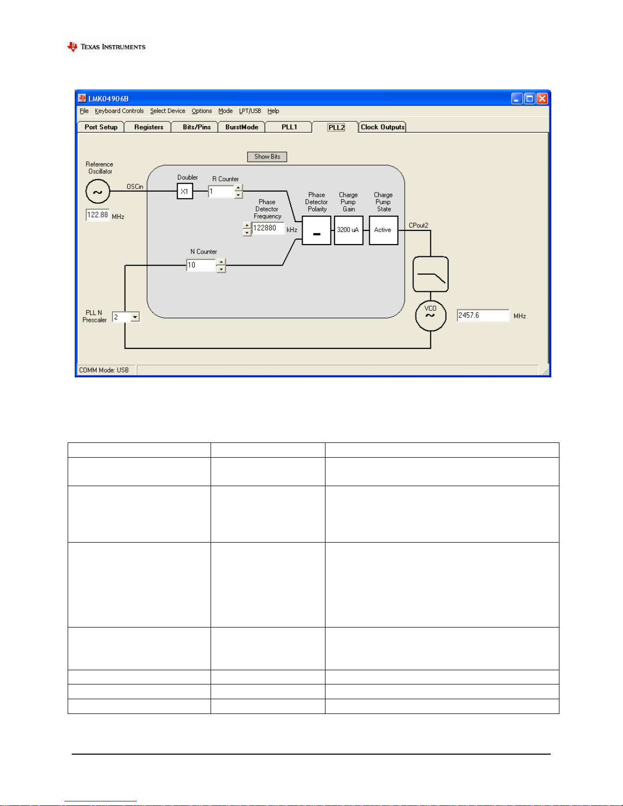
This tab also allows the user to select the VCO Divider value (2 to 8). Note that the total PLL2
N divider value is the product of the VCO Divider value and the PLL N Prescaler and N Counter
values (shown in the PLL2 tab), and is given by:
SNAU126
Page 27

L M K 0 4 9 0 6 E V A L U A T I O N B O A R D O P E R A T I N G I N S T R U C T I O N S
27
PLL2 N Total = VCO Divider * PLL2 N Prescaler * PLL2 N Counter
Clicking on the cyan-colored PLL2 block that contains R, PDF and N values will bring the
PLL2 tab into focus where these values may be modified, if needed.
Clicking on the values in the box containing the Internal Loop Filter component (R3, C3, R4,
C4) allow one to step through the possible values. Left click to increase the component value,
and right click to decrease the value. These values can also be changed in the Bits/Pins tab.
The Reference Oscillator value field may be changed in either the Clock Outputs tab or the
PLL2 tab. The PLL2 Reference frequency should match the frequency of the onboard VCXO or
Crystal (i.e. VCO frequency in the PLL1 tab); if not, a warning message will appear to indicate
that the PLL(s) may be out of lock, as highlighted by the red box in Figure 10.
Figure 10: Warning message indicating mismatch between
PLL1 VCO frequency (30.72MHz) and PLL2 reference frequency (122.88 MHz)
SNAU126
Page 28

L M K 0 4 9 0 6 E V A L U A T I O N B O A R D O P E R A T I N G I N S T R U C T I O N S
28
Control Name
Register Name
Description
Reference Oscillator
Frequency (MHz)
n/a
CLKin frequency of the selected reference
clock.
Phase Detector Frequency
(MHz)
n/a
PLL1 Phase Detector Frequency (PDF).
This value is calculated as:
PLL1 PDF = CLKin Frequency / (PLL1_R *
CLKinX_PreR_DIV), where
CLKinX_PreR_DIV is the predivider value
of the selected input clock.
PLL1 Tab
Figure 11: PLL1 tab
The PLL1 tab allows the user to change the following parameters in Table 8.
Table 8: Registers Controls and Descriptions in PLL1 tab
SNAU126
Page 29

L M K 0 4 9 0 6 E V A L U A T I O N B O A R D O P E R A T I N G I N S T R U C T I O N S
29
VCO Frequency (MHz)
n/a
The VCO Frequency should be the OSCin
frequency, except when operating in Dual
PLL with 0-delay feedback. This value is
calculated as:
VCO Freq (OSCin freq) = PLL1 PDF *
PLL1_N.
In Dual PLL mode with 0-delay feedback,
the VCO frequency should be set to the
feedback clock input frequency. See the
section Setting the PLL1 VCO Frequency
and PLL2 Reference Frequency for details.
R Counter
PLL1_R
PLL1 R Counter value (1 to 16383).
N Counter
PLL1_N
PLL1 N Counter value (1 to 16383).
Phase Detector Polarity
PLL1_CP_POL
PLL1 Phase Detector Polarity.
Click on the polarity sign to toggle polarity
“+” or “–”.
Charge Pump Gain
PLL1_CP_GAIN
PLL1 Charge Pump Gain.
Left-click/right-click to increase/decrease
charge pump gain (100, 200, 400, 1600 uA).
Charge Pump State
PLL1_CP_TRI
PLL1 Charge Pump State.
Click to toggle between Active and Tri-State.
Setting the PLL1 VCO Frequency and PLL2 Reference Frequency
When operating in Dual PLL mode without 0-delay feedback, the VCO frequency value on the
PLL1 tab must match the Reference Oscillator (OSCin) frequency value on the PLL2 tab;
otherwise, the one or both PLLs may be out of lock. Updating the Reference Oscillator
frequency on the PLL2 tab will automatically update the value of OSCin_FREQ on the
Bits/Pins tab.
However, when operating in Dual PLL mode with 0-delay feedback, it may be valid for the VCO
frequency value on the PLL1 tab to be different from the Reference Oscillator (OSCin)
frequency value on the PLL2 tab. This is because in 0-delay mode, the PLL1 feedback clock is
taken from an output clock instead of the OSCin clock. For example, if the CLKin frequency (to
PLL1_R) is 30.72 MHz, the 0-delay feedback clock frequency (to PLL1_N) is 30.72 MHz, and
the VCXO frequency is 122.88 MHz, then the VCO frequency value on the PLL1 tab should be
30.72 MHz (0-delay feedback frequency) and the Reference Oscillator frequency value on the
PLL2 tab should be 122.88 MHz (VCXO frequency). Because of the mismatched frequencies, a
warning message will indicate this condition on the Clock Outputs tab but may be disregarded
in a case like this.
SNAU126
Page 30
L M K 0 4 9 0 6 E V A L U A T I O N B O A R D O P E R A T I N G I N S T R U C T I O N S
30
Control Name
Register Name
Description
Reference Oscillator
Frequency (MHz)
OSCin_FREQ
OSCin frequency from the External VCXO
or Crystal.
Phase Detector Frequency
(MHz)
n/s
PLL2 Phase Detector Frequency (PDF).
This value is calculated as:
PLL2 PDF = OSCin Frequency
*(2
EN_PLL2_REF_2X
) / PLL2_R.
VCO Frequency (MHz)
n/a
Internal VCO Frequency should be within
the allowable range of the LMK04906B
device.
This value is calculated as:
VCO Frequency = PLL2 PDF * (PLL2_N *
PLL2_P * VCO divider value).
Doubler
EN_PLL2_REF_2X
PLL2 Doubler.
0 = Bypass Doubler
1 = Enable Doubler
R Counter
PLL2_R
PLL2 R Counter value (1 to 4095).
N Counter
PLL2_N
PLL2 N Counter value (1 to 262143).
PLLN Prescaler
PLL2_P
PLL2 N Prescaler value (2 to 8).
PLL2 Tab
Figure 12: PLL2 tab
The PLL2 tab allows the user to change the following parameters in Table 9.
Table 9: Registers Controls and Descriptions in PLL2 tab
SNAU126
Page 31

L M K 0 4 9 0 6 E V A L U A T I O N B O A R D O P E R A T I N G I N S T R U C T I O N S
31
Phase Detector Polarity
PLL2_CP_POL
PLL2 Phase Detector Polarity.
Click on the polarity sign to toggle polarity
“+” or “–”.
Charge Pump Gain
PLL2_CP_GAIN
PLL2 Charge Pump Gain.
Left-click/right-click to increase/decrease
charge pump gain (100, 400, 1600, 3200
uA).
Charge Pump State
PLL2_CP_TRI
PLL2 Charge Pump State.
Click to toggle between Active and Tri-State.
Changes made on this tab will be reflected in the Clock Outputs tab. The VCO Frequency
should conform to the specified internal VCO frequency range for the LMK04906B device (per
Table 2).
Bits/Pins Tab
Figure 13: Bits/Pins tab
The Bits/Pins tab allows the user to program bits directly, many of which are not available on
other tabs. Brief descriptions for the controls on this tab are provided in Table 10 to supplement
the datasheet. Refer to the LMK04906 Family Datasheet for more information.
TIP: Right-clicking any register name in the Bits/Pins tab will display a Help prompt with the
register address, data bit location/length, and a brief register description.
SNAU126
Page 32

L M K 0 4 9 0 6 E V A L U A T I O N B O A R D O P E R A T I N G I N S T R U C T I O N S
32
Group
Register Name
Description
Mode Control
RESET
Resets the device to default register values. RESET
must be cleared for normal operation to prevent an
unintended reset every time R0 is programmed.
POWERDOWN
Places the device in powerdown mode.
MODE
Selects the operating mode (topology) for the
LMK04906 device.
PD_OSCin
Powers down the OSCin buffer. For use in Clock
Distribution mode if OSCin path is not used.
FEEDBACK_MUX
Selects the feedback source for 0-delay mode.
OSCin_FREQ
Must be set to the OSCin frequency range for
PLL2. Used for proper operation of the internal
VCO calibration routine.
Entering a reference oscillator frequency on PLL2
tab will automatically update OSCin_FREQ to the
proper frequency range.
VCO_MUX
Selects between VCO and VCO divider to drive the
clock distribution path. The VCO divider is only
valid if MODE is selecting the Internal VCO.
uWire_LOCK
When checked, no other uWire programming will
have effect. Must be unchecked to enable uWire
programming of registers R0 to R30.
CLKin
CLKin_Select_MODE
Selects operational mode for how the device selects
the reference clock for PLL1.
EN_CLKin1
Enables CLKin1 as a usable reference input during
auto switching mode.
EN_CLKin0
Enables CLKin0 as a usable reference input during
auto switching mode.
CLKinX_BUF_TYPE
Selects the CLKinX input buffer to Bipolar
(internal 0 mV offset) or MOS (internal 55 mV
offset).
EN_LOS
Enable the Loss-Of-Signal (LOS) detect circuitry.
LOS_TIMEOUT
Sets the timeout value for the LOS detect circuitry
to assert a loss of signal state on a clock input.
Crystal
EN_PLL2_XTAL
Enables Crystal Oscillator
XTAL_LVL
Sets peak amplitude on the tunable crystal. Values
listed are for a 20.48 MHz crystal.
IO Control
LD_MUX
Sets the selected signal on the Status_LD pin.
LD_TYPE
Sets I/O pin type on the Status_LD pin.
HOLDOVER_MUX
Sets the selected signal on the Status_HOLDOVER
pin.
HOLDOVER_TYPE
Sets I/O pin type on the Status_Holdover pin.
Table 10: Register Controls and Descriptions on Bits/Pins tab
SNAU126
Page 33

L M K 0 4 9 0 6 E V A L U A T I O N B O A R D O P E R A T I N G I N S T R U C T I O N S
33
Status_CLKin0 _MUX
Sets the selected signal on the Status_CLKin0 pin.
Status_CLKin0_TYPE
Sets I/O pin type on the Status_CLKin0 pin.
Status_CLKin1_MUX
Sets the selected signal on the Status_CLKin1 pin.
Status_CLKin1_TYPE
Sets I/O pin type on the Status_CLKin1 pin.
CLKin_Sel_INV
Inverts the Status_CLKin0/1 pin polarity when set
to an input type. Significant when
CLKin_SELECT_MODE is 3 or 6.
IO Control – Sync
SYNC_MUX
Sets the selected signal on the SYNC pin.
SYNC_TYPE
Sets I/O pin type on the SYNC pin.
SYNC_POL_INV
Sets polarity on SYNC input to active low when
checked. Toggling this bit will initiate a SYNC
event.
SYNC_PLL1_DLD
Engage SYNC mode until PLL1 DLD is true
SYNC_PLL2_DLD
Engage SYNC mode until PLL2 DLD is true
NO_SYNC_CLKoutX_Y
Synchronization will not affect selected clock
outputs, where X = even-numbered output and Y =
odd-numbered output.
SYNC_QUAL
Sets the SYNC to qualify mode for dynamic digital
delay.
EN_SYNC
Must be set when using SYNC, but may be cleared
after the SYNC event. When using dynamic digital
delay (SYNC_QUAL = 1), EN_SYNC must always
be set.
Changing this value from 0 to 1 can cause a SYNC
event, so clocks which should not be SYNCed
when setting this bit should have the
NO_SYNC_CLKoutX_Y bit set.
NOTE: This bit is not a valid method of generating
a SYNC event. Use one of the other SYNC
generation methods to ensure a proper SYNC
occurs.
SYNC_EN_AUTO
Enable auto SYNC when R0 to R5 is written.
DAC/Holdover
HOLDOVER_MODE
Sets holdover mode to be disabled or enabled.
FORCE_HOLDOVER
Engages holdover when checked regardless of
HOLDOVER_MODE value. Turns the DAC on.
EN_TRACK
Enables DAC tracking. DAC tracks the PLL1
Vtune to provide for an accurate HOLDOVER
mode. DAC_CLK_DIV should also be set so that
DAC update rate is <= 100 kHz.
EN_VTUNE_RAIL_DET
Allows rail-to-rail operation of VCXO with default
of 0. Allows use of DAC_LOW_TRIP,
DAC_HIGH_TRIP. Must be used with
EN_MAC_DAC = 1. CLKin_SELECT_MODE
must be 4 or 6 (auto mode) to use.
SNAU126
Page 34

L M K 0 4 9 0 6 E V A L U A T I O N B O A R D O P E R A T I N G I N S T R U C T I O N S
34
HOLD_DLD_CNT
In HOLDOVER mode, wait for this many clocks of
PLL1 PDF within the tolerances of PLL1_WND
_SIZE before exiting holdover mode.
DAC_CLK_DIV
DAC update clock is the PLL1 phase detector
divided by this divisor. For proper operation, DAC
update clock rate should be <= 100 kHz.
DAC update rate = PLL1 phase detector frequency /
DAC_CLK_DIV
EN_MAN_DAC
Enables manual DAC mode and set DAC voltage
when in holdover.
MAN_DAC
Sets the value for the DAC when EN_MAN_DAC
is 1 and holdover is engaged. Readback from this
register is the current DAC value whether in
manual DAC mode or DAC tracking mode
DAC_LOW_TRIP
Value from GND in ~50mV steps at which a clock
switch event is generated. If Holdover mode is
enabled, it will be engaged upon the clock switch
event.
NOTE: EN_VTUNE_RAIL_DET must be enabled
for this to be valid.
DAC_HIGH_TRIP
Value from VCC (3.3V) in ~50mV steps at which
clock switch event is generated. If Holdover mode
is enabled, it will be engaged upon the clock switch
event.
NOTE: EN_VTUNE_RAIL_DET must be enabled
for this to be valid.
PLL1
PLL1_WND_SIZE
If the phase error between the PLL1 reference and
feedback clocks is less than specified time, then the
PLL1 lock counter increments.
NOTE: Final lock detect valid signal is determined
when the PLL1 lock counter meets or exceeds the
PLL1_DLD_CNT value.
PLL1_DLD_CNT
The reference and feedback of PLL1 must be within
the window of phase error as specified by
PLL1_WND_SIZE for this many cycles before
PLL1 digital lock detect is asserted.
CLKinX_PreR_DIV
The PreR dividers divide the CLKinX reference
before the PLL1_R divider.
Unique divides on individual CLKinX signals
allows switchover from one clock input to another
clock input without needing to reprogram the
PLL1_R divider to keep the device in lock.
PLL1_N_DLY
N delay causes clock outputs to lead clock input
when in a 0-delay mode. Increasing the N delay
value increases the output phase lead relative to the
input.
SNAU126
Page 35

L M K 0 4 9 0 6 E V A L U A T I O N B O A R D O P E R A T I N G I N S T R U C T I O N S
35
PLL1_R_DLY
R delay causes clock outputs to lag clock input
when in a 0-delay mode. Increasing the R delay
value increases the output phase lag relative to the
input.
PLL2
PLL2_WND_SIZE
If the phase error between the PLL2 reference and
feedback clock is less than specified time, then the
PLL2 lock counter increments.
PLL2_DLD_CNT
The reference and feedback of PLL2 must be within
the window of phase error as specified by
PLL2_WND_SIZE for this many cycles before
PLL2 digital lock detect is asserted.
EN_PLL2_REF_2X
Enables the doubler block to doubles the reference
frequency into the PLL2 R counter. This can allow
for frequency of 2/3, 2/5, etc. of OSCin to be used
at the phase detector of PLL2.
PLL2_N_CAL
The PLL2_N_CAL register contains the N value
used for the VCO calibration routine. Except
during 0-delay modes, the PLL2_N and
PLL2_N_CAL registers will be exactly the same.
PLL2_R3_LF
Set the corresponding integrated PLL2 loop filter
values: R3, R4, C3, and C4.
It is also possible to set these values by clicking on
the loop filter values on the Clock Outputs tab.
PLL2_R4_LF
PLL2_C3_LF
PLL2_C4_LF
PLL2_FAST_PDF
Enable this bit when using a PLL2 phase detector
frequency > 100 MHz.
Program Pins
SYNC
Sets these pins on the uWire header to logic high
(checked) or logic low (unchecked).
Status_CLKin0
Status_CLKin1
SNAU126
Page 36

L M K 0 4 9 0 6 E V A L U A T I O N B O A R D O P E R A T I N G I N S T R U C T I O N S
36
Registers Tab
Figure 14: Registers Tab
The Registers tab shows the value of each register. This is convenient for programming the
device to the desired settings, then exporting to a text file the register values in hexadecimal for
use in your own application.
By clicking in the “bit field” it is possible to manually change the value of registers by typing „1‟
and „0.‟
SNAU126
Page 37

L M K 0 4 9 0 6 E V A L U A T I O N B O A R D O P E R A T I N G I N S T R U C T I O N S
37
Parameter
Value
PLL1 Reference clock input
CLKin0 single-ended input, CLKin0* AC-coupled to GND
PLL1 Reference Clock frequency
122.88 MHz
PLL1 Phase detector frequency
122.88 MHz
PLL1 Charge Pump Gain
100 uA
VCXO frequency
122.88 MHz
PLL2 phase detector frequency
122.88 MHz
PLL2 Charge Pump Gain
3200 uA
PLL2 REF2X mode
Disabled
Appendix B: Typical Phase Noise Performance Plots
PLL1
The LMK04906B‟s dual PLL architecture achieves ultra low jitter and phase noise by allowing
the external VCXO or Crystal‟s phase noise to dominate the final output phase noise at low
offset frequencies and the internal VCO‟s phase noise to dominate the final output phase noise at
high offset frequencies. This results in the best overall noise and jitter performance.
Table 11 lists the test conditions used for output clock phase noise measurements with the
Crystek 122.88 MHz VCXO.
Table 11: LMK04906B Test Conditions
122.88 MHz VCXO Phase Noise
The phase noise of the reference is masked by the phase noise of this VCXO by using a narrow
loop bandwidth for PLL1 while retaining the frequency accuracy of the reference clock input.
This VCXO sets the reference noise to PLL2. Figure 15 shows the open loop typical phase noise
performance of the CVHD-950-122.88 Crystek VCXO.
SNAU126
Page 38

L M K 0 4 9 0 6 E V A L U A T I O N B O A R D O P E R A T I N G I N S T R U C T I O N S
38
Table 12: VCXO Phase Noise
at 122.88 MHz (dBc/Hz)
Offset
Phase
Noise
10 Hz
-76.6
100 Hz
-108.9
1 kHz
-137.4
10 kHz
-153.3
100 kHz
-162.0
1 MHz
-165.7
10 MHz
-168.1
40 MHz
-168.1
Table 13: VCXO RMS Jitter
to high offset of 20 MHz
at 122.88 MHz (rms fs)
Low
Offset
Jitter
10 Hz
515.4
100 Hz
60.5
1 kHz
36.2
10 kHz
35.0
100 kHz
34.5
1 MHz
32.9
10 MHz
22.7
VCXO Phase Noise
-170
-160
-150
-140
-130
-120
-110
-100
-90
-80
-70
-60
-50
10 100 1000 10000 100000 1000000 10000000 1E+08
Offset (Hz)
Phase Noise (dBc/Hz)
CVHD-950-122.88
Figure 15: Crystek CVHD-950-122.88 MHz VCXO Phase Noise at 122.88 MHz
Clock Output Measurement Technique
The same technique was used to measure phase noise for all three output types available on the
programmable OSCout and CLKout buffers. This was achieved by terminating one side of the
LVPECL, LVDS, or LVCMOS output with a 50-ohm load, and measuring the other side singleended using an Agilent E5052B Source Signal Analyzer.
Buffered OSCout Phase Noise
Both OSCout0 frequencies are 122.88 MHz since the OSCout Divider is bypassed. OSCout0 is
programmed to LVCMOS mode.
SNAU126
Page 39

L M K 0 4 9 0 6 E V A L U A T I O N B O A R D O P E R A T I N G I N S T R U C T I O N S
39
Offset
1474.56 MHz
LVDS
1474.56 MHz
LVPECL
491.52 MHz
LVDS
491.52 MHz
LVPECL
100 Hz
-88.9
-88.3
-99.9
-99.0
1 kHz
-109.1
-109.5
-117.7
-119.5
10 kHz
-119.0
-119.1
-126.9
-126.5
100 kHz
-121.2
-121.2
-129.4
-129.5
800 kHz
-133.6
-133.6
-141.6
-141.7
1 MHz
-135.4
-135.5
-143.5
-143.6
10 MHz
-149.9
-151.0
-154.2
-156.2
20 MHz
-150.6
-151.6
-154.2
-156.5
RMS Jitter (fs)
10 kHz to 20 MHz
95.3
94.4
97.5
94.3
RMS Jitter (fs)
100 Hz to 20 MHz
110.8
109.9
111.9
108.6
Clock Outputs (CLKout)
The LMK04906 Family features programmable LVDS, LVPECL, and LVCMOS buffer modes
for the CLKoutX and OSCout0 output pairs. Included below are various phase noise
measurements for each output format.
LMK04906B CLKout Phase Noise
Figure 16: LMK04906B CLKout Phase Noise
Table 14: LMK04906B Phase Noise (dBc/Hz) Phase Noise and RMS Jitter (fs)
SNAU126
Page 40

L M K 0 4 9 0 6 E V A L U A T I O N B O A R D O P E R A T I N G I N S T R U C T I O N S
40
Offset
245.76
LVDS
245.76
LVPECL
245.76
LVCMOS
122.88
LVDS
122.88
LVCMOS
122.88
LVPECL
100 Hz
-106.2
-103.4
-102.9
-110.3
-110.5
-108.1
1 kHz
-124.8
-124.0
-124.1
-130.2
-130.2
-130.8
10 kHz
-133.0
-132.7
-133.7
-139.2
-137.4
-139.1
100 kHz
-135.6
-135.6
-135.7
-141.8
-141.7
-141.8
800 kHz
-147.8
-147.8
-148.3
-152.9
-153.4
-153.4
1 MHz
-149.1
-149.5
-149.2
-154.5
-155.1
-155.0
10 MHz
-156.9
-159.0
-158.0
-158.5
-161.5
-161.4
20 MHz
-157.0
-159.1
-158.1
-158.5
-161.6
-161.5
RMS Jitter (fs)
10 kHz to 20 MHz
105.1
98.1
101.7
131.1
110.7
110.6
RMS Jitter (fs)
100 Hz to 20 MHz
118.0
113.0
118.0
141.7
123.9
123.8
For the LMK04906B, the internal VCO frequency is 2949.12 MHz. The divide-by-12 CLKout
frequency is 245.76 MHz, and the divide-by-24 CLKout frequency is 122.88 MHz.
Table 15: LMK04906B Phase Noise and RMS Jitter for Different CLKout Output Formats and Frequencies
SNAU126
Page 41

L M K 0 4 9 0 6 E V A L U A T I O N B O A R D O P E R A T I N G I N S T R U C T I O N S
41
Offset
OSCout0
LVPECL
OSCin thru
CLKout
100 Hz
-106.8
-104.7
1 kHz
-135.5
-133.1
10 kHz
-147.8
-147.3
100 kHz
-155.5
-154.4
800 kHz
-157.6
-156.1
1 MHz
-157.5
-156.2
10 MHz
-158.6
-155.7
20 MHz
-158.4
-157.1
RMS Jitter (fs)
10 kHz to 20 MHz
103.6
121.3
RMS Jitter (fs)
100 Hz to 20 MHz
118.4
135.3
LMK04906B OSCout Phase Noise
Figure 17: LMK04906B OSCout Phase Noise
Table 16: LMK04906B OSCout Phase Noise and RMS Jitter (fs)
SNAU126
Page 42
L M K 0 4 9 0 6 E V A L U A T I O N B O A R D O P E R A T I N G I N S T R U C T I O N S
SNAU126
42
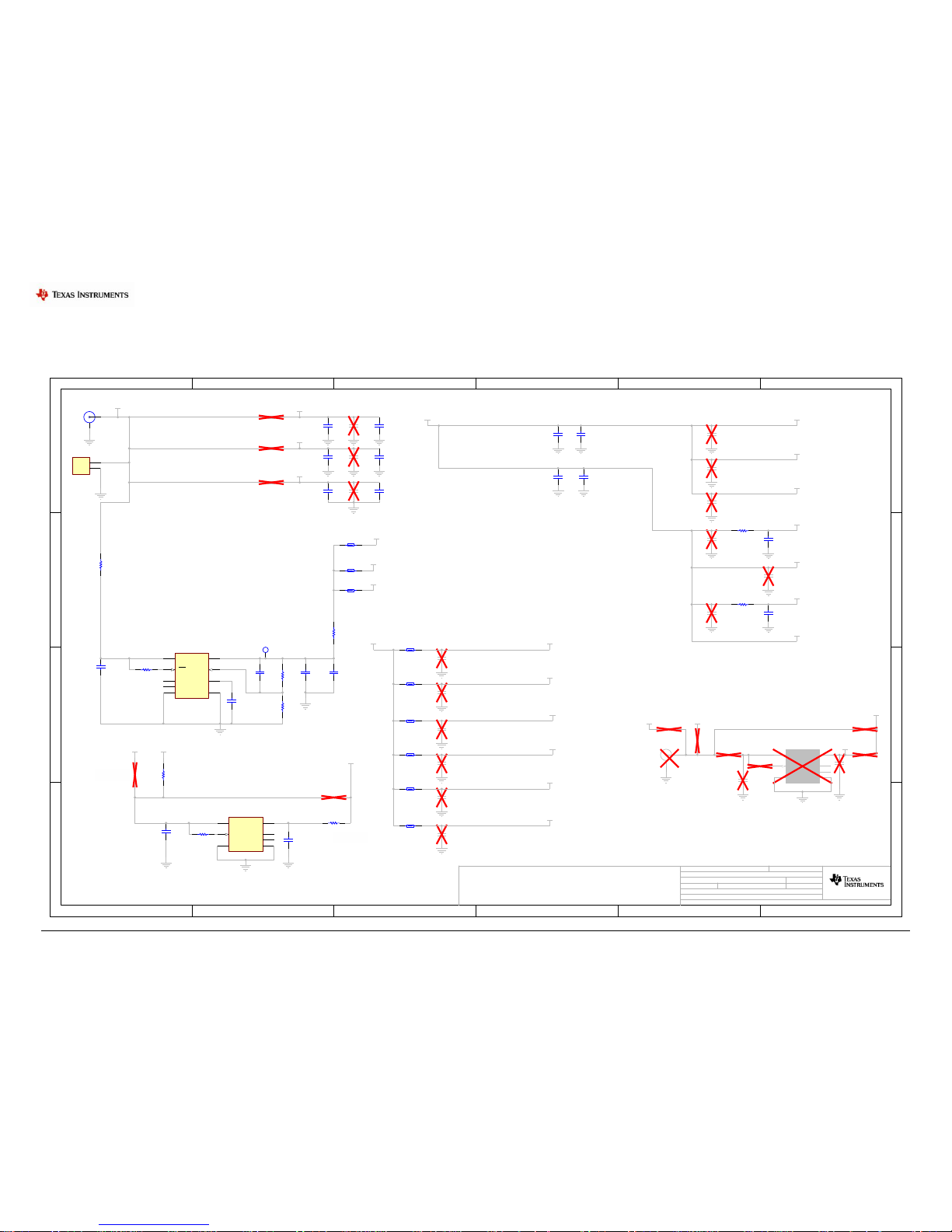
Appendix C: Schematics
Power Supplies
1
1
2
2
3
3
4
4
5
5
6
6
D D
C C
B B
A A
2 8Power Supplies
1/25/2012
Power.SchDoc
Sheet Title:
Size: Schematic:
Mod. Date:
File:
Rev:
Sheet: of
B
Texas Instruments and/or its licensors do not warrant the accuracy or completeness of this
specification or any information contained therein. Texas Instruments and/or its licensors do not
warrant that this design will meet the specifications, will be suitable for your application or fit for
any particular purpose, or will operate in an implementation. Texas Instruments and/or its
licensors do not warrant that the design is production worthy. You should completely validate
and test your design implementation to confirm the system functionality for your application.
http://www.ti.com
Contact: http://www.national.com/support
LMK049xx Evaluation BoardProject:
Designed for:Evaluation Customer
870600738 1
Assembly Variant:12-21-2011
© Texas Instruments CopyrightYear
VccPLLPlane
0.1µF
C81
FB 1000 ohm 600 mA
R96
DNP
FB 1000 ohm 600 mA
R98
DNP
VccCLKoutPlane
FB 1000 ohm 600 mA
R97
DNP
0.1µF
C78
LDO Power Options
Power Plane for LMK Except Outputs
Power Planes for LMK CLKout Outputs
Vcc
VccAuxPlane
VccCLKoutPlane
VccPLLPlane
Direct Power
120
R103
VccAuxPlane
IN
4
ADJ
6
GND
3
NC
7
SD
8
DAP
9
OUT
5
BYP1NC
2
U5
LP3878SD-ADJ
LP3878-ADJ 3.3 V component values:
C340 = 4.7 uF
R350= 51 k
C346 = 0.01 uF R356= 866
C352 = 10 uF
R351= 2.00 k
C341 = 2.2 nF
0.1µF
C72
1µF
C71
1µF
C89
DNP
1µF
C93
DNP
1
1
2
2
J1
TERMBLOCK_2
IN6OUT
1
GND
3
EN
4
NC
5
DAP
7
NC
2
U7
LP5900SD-3.3
GND
C359 = 0.47 uF
C360 = 0.47 uF
R369 = 51 k
Designators greater than and equal to 300 are placed on bottom of PCB
LP3878SD-ADJ
LP5900SD-3.3
LP5900 Component values
0
R99
FB 120 ohm
R104
120
R106
0.1µF
C63
1µF
C62
DNP
10µF
C61
0.1µF
C69
1µF
C68
DNP
10µF
C67
0.1µF
C75
1µF
C74
DNP
10µF
C73
Aux Power for XO/VCXO
0.1µF
C65
1µF
C64
1µF
C82
DNP
Vcc2_CLKout_CG1
Vcc1_VCO
Vcc4_Digital
Vcc5_CLKin
Vcc6_PDCP1
Vcc7_OSC
Vcc8_PDCP2
Vcc9_PLL2
CG3
CG4
CG5
CG0
CG2
CG1
Vcc13_CLKout_CG0
VCO
Digital
CLKin
PDCP1
OSC
PDCP2
PLL2
0
R101
0
R105
120
R111
Vcc_VCO
VccAuxPlane
0
R112
DNP
120
R100
VccCLKoutPlane
120
R102
VccPLLPlane
LDO_Out_LP3878
TESTPOINT
0.1µF
C66
DNP
0.1µF
C70
DNP
100pF
C76
DNP
0.1µF
C77
DNP
100pF
C79
DNP
0.1µF
C80
DNP
51k
R107
0.01µF
C88
2.00k
R108
866
R110
51k
R125
0.47µF
C94
0.47µF
C96
0
R122
DNP
4.7µF
C83
1µF
C85
2200pF
C84
Vcc10_CLKout_CG3
Vcc11_CLKout_CG4
Vcc3_CLKout_CG2
Vcc12_CLKout_CG5
1µF
C95
DNP
1µF
C90
DNP
1µF
C87
DNP
120
R109
120
R115
120
R124
120
R121
IN6OUT
1
GND
3
EN
4
NC
5
DAP
7
NC
2
U6
LP5900SD-3.3
DNP
GND
C359 = 0.47 uF
C360 = 0.47 uF
R369 = 51 k
LP5900SD-3.3
LP5900 Component values
51k
R118
DNP
0.47µF
C92
DNP
0.47µF
C91
DNP
Vcc
0
R114
DNP
0
R117
DNP
Vcc_VCO_LDO
0
R113
DNP
0
R116
DNP
Vcc_VCXO
0
R123
Switch resistor
for power.
10µF
C86
Vcc
0
R120
VccAuxPlane
0
R119
DNP
Switch resistor
for power.
Vcc
VccVCO/Aux
DNP
Page 43

L M K 0 4 9 0 6 E V A L U A T I O N B O A R D O P E R A T I N G I N S T R U C T I O N S
SNAU126
43
LMK04906B Device with Loop Filter and Crystal Circuits
1
1
2
2
3
3
4
4
5
5
6
6
D D
C C
B B
A A
3 8Main Sheet / IC
12/21/2011
LMK049xx_PLL.SchDoc
Sheet Title:
Size: Schematic:
Mod. Date:
File:
Rev:
Sheet: of
B
Texas Instruments and/or its licensors do not warrant the accuracy or completeness of this
specification or any information contained therein. Texas Instruments and/or its licensors do not
warrant that this design will meet the specifications, will be suitable for your application or fit for
any particular purpose, or will operate in an implementation. Texas Instruments and/or its
licensors do not warrant that the design is production worthy. You should completely validate
and test your design implementation to confirm the system functionality for your application.
http://www.ti.com
Contact: http://www.national.com/support
LMK049xx Evaluation BoardProject:
Designed for:Evaluation Customer
870600738 1
Assembly Variant: 12-21-2011
© Texas Instruments CopyrightYear
100pF
C2p_VCO
DNP
0.1µF
C38
DNP
0.1µF
C30
0.68µF
C2_VCXO
0
R40
DNP
2pF
C36
DNP
2200pF
C34
DNP
2pF
C31
DNP
2200pF
C32
DNP
PLL2 Loop Filter
PLL1 Loop Filter
OSCin Tuneable Crystal
4.7k
R36
DNP
1000pF
C33
DNP
10k
R38
DNP
VCXO Loop Filter
Y300
DNP
DNP
VTUNE2_TP
0
R42
Designators greater than and equal to 200 are placed on bottom of PCB
10µF
C37
0.1µF
C39
CLKout0_P
CLKout0_N
CLKout1_P
CLKout1_N
CLKout2_P
CLKout2_N
CLKin0_P
CLKin0_N
CLKin1_P
CLKin1_N
CLKin2_P
CLKin2_N
Status_Hold
Status_LD
Status_CLKin0
Status_CLKin1
CLKout5_N
CLKout5_P
CLKout4_N
CLKout4_P
CLKout3_N
CLKout3_P
SYNC
0
R35
DNP
uWire_DATA
uWire_CLK
uWire_LE
OSCout0_N
OSCout0_P
Vcc1_VCO
Vcc2_CLKout_CG1
Vcc3_CLKout_CG2
Vcc4_Digital Vcc5_CLKin
Vcc6_PDCP1
Vcc7_OSC
Vcc9_PLL2
Vcc12_CLKout_CG5
Vcc13_CLKout_CG0
Vcc8_PDCP2
OSCin_N
OSCin_P
4.7k
R39
DNP
VTUNE1_TP
Vtune_VCXO
Status_Hold
SYNC
Status_LD
Status_CLKin0
Status_CLKin1
uWire_LE
uWire_DATA
uWire_CLK
0.1µF
C35
DNP
0
R43
VCO_Vtune
0
R34
DNP
0.1µF
C40
0.1µF
C1_VCXO
2.7µF
C2A_VCXO
DNP
39k
R2_VCXO
620
R2_VCO
47pF
C1_VCO
3900pF
C2_VCO
OSCin_1_N
OSCin_1_P
1
3
2
SMV1249-074LF
D1
DNP
CPout1
Vcc10_CLKout_CG3
Vcc11_CLKout_CG4
OSCin_1_N
OSCin_1_P
51
R37
DNP
Vcc13
1
NC
2
CLKout0
4
CLKout0*
3
NC
5
SYNC/Status_CLKin2
6
NC
7
NC
8
NC
9
Vcc1
10
LDObyp1
11
LDObyp2
12
NC19CLKout2*20NC22CLKout221GND23Vcc424FBCLKin/CLKin125FBCLKin*/CLKin1*26Status_Holdover27CLKin028CLKin0*29Vcc5
30
Vcc6
35
OSCin
36
OSCin*
37
Vcc7
38
OSCout0
39
OSCout0*
40
Vcc8
41
CPout2
42
Vcc9
43
LEuWire
44
CLKuWire
45
DATAuWire
46
NC
51
Vcc11
52
CLKout4
53
CLKout4*
54NC55NC56
Vcc12
57
CLKout5
58
CLKout5*
59NC60NC61
Status_CLKin0
62
LMK04906
DAP PAD
0
CLKout1
13
CLKout1*
14
NC
15
Vcc2
16
NC17Vcc3
18
CLKin231CLKin2*
32
Status_LD
33
CPout1
34
NC
47
Vcc10
48
CLKout3
49
CLKout3*
50
Status_CLKin1
63NC64
U1
Used in BOM report
Vtune_XTAL
0
R41
DNP
Vtune_XTAL
100pF
C3_VCXO
Page 44

L M K 0 4 9 0 6 E V A L U A T I O N B O A R D O P E R A T I N G I N S T R U C T I O N S
SNAU126
44
Reference Inputs (CLKin0, CLKin1 & CLKin2), External VCXO (OSCin) & VCO Circuits
1
1
2
2
3
3
4
4
5
5
6
6
D D
C C
B B
A A
5 8Clock Inputs
1/25/2012
InClks.SchDoc
Sheet Title:
Size: Schematic:
Mod. Date:
File:
Rev:
Sheet: of
B
Texas Instruments and/or its licensors do not warrant the accuracy or completeness of this
specification or any information contained therein. Texas Instruments and/or its licensors do not
warrant that this design will meet the specifications, will be suitable for your application or fit for
any particular purpose, or will operate in an implementation. Texas Instruments and/or its
licensors do not warrant that the design is production worthy. You should completely validate
and test your design implementation to confirm the system functionality for your application.
http://www.ti.com
Contact: http://www.national.com/support
LMK049xx Evaluation BoardProject:
Designed for:Evaluation Customer
870600738 1
Assembly Variant: 12-21-2011
© Texas Instruments CopyrightYear
0.1µF
C15
18
R19
270
R20
0.1µF
C19
0.1µF
C14
DNP
100pF
C20
DNP
FBCLKin/CLKin1 Impedance Matching and Attenuation
CLKin1
0
R2
270
R4
DNP
0.1µF
C2
0.1µF
C10
0.1µF
C6
DNP
100
R5
0.1µF
C1
0
R8
0.1µF
C9
CLKin0 Impedance Matching and Attenuation
270
R11
DNP
0.1µF
C11
DNP
0.1µF
C25
0.1µF
C28
270
R29
DNP
270
R33
DNP
CLKin2 Impedance Matching and Attenuation
Vcc_VCO
100pF
C17
DNP
0.1µF
C16
0
R15
DNP
CLKin0_P
CLKin0_N
CLKin1_P
CLKin1_N
CLKin2_P
CLKin2_N
0.1µF
C27
0.1µF
C24
0
R27
0
R31
270
R28
DNP
270
R32
DNP
100
R30
GND
3
Vtune
2
GND
1
GND7Mod6GND5GND
8
GND4GND
9
Fout
10
GND
11
GND
12
GND
13
Vcc
14
GND15GND
16
U3
CRO2949A-LF
DNP
0.1µF
C21
DNP
0.1µF
C18
DNP
0
R24
DNP
10k
R25
DNP
10k
R26
DNP
Vcc_VCO_OpAmp
0
R23
DNP
Vcc_VCO_OpAmp
4
3
2
1
5
V+
V-
U4
LMP7731MF
DNP
VCO_Vtune
PLL2 External VCO Loop Filter
Vcc_VCO_LDO
0.1µF
C23
DNP
0
R22
DNP
270
R21
0.1µF
C22
DNP
CLKin0*
SMA
CLKin0
SMA
FBCLKin*/CLKin1*
SMA
CLKin2*
SMA
CLKin2
SMA
CLKin2_2_N
CLkin2_2_P
CLKin0_2_N
CLKin0_2_P
0.1uF
C29
DNP
270
R10
DNP
270
R3
DNP
Vtune
1
NC
2
GND3RF
4
RF*
5
Vs
6
U2
CVHD-950-122.88
OSCin VCXO
8.2
R12
DNP
8.2
R9
DNP
140
R7
DNP
0
R14
0.1µF
C7
DNP
0.1µF
C13
DNP
0.1µF
C12
0.1µF
C8
DNP
120
R1
OSCin_1_N
OSCin_1_P
OSCin
SMA
DNP
OSCin*
SMA
DNP
10µF
C3
2200pFC482pF
C5
Switch capacitor for signal
(shared pad)
Switch capacitor for signal
(shared pad)
0
R16
Vtune_VCXO
VCC_VCXO_TP
Vcc_VCXO
0.1uF
C26
DNP
CLKin2_1_P
CLKin2_1_N
0
R13
140
R6
DNP
120
R17
DNP
120
R18
DNP
Page 45

L M K 0 4 9 0 6 E V A L U A T I O N B O A R D O P E R A T I N G I N S T R U C T I O N S
SNAU126
45
Clock Outputs (OSCout0, CLKout0 to CLKout5)
1
1
2
2
3
3
4
4
5
5
6
6
D D
C C
B B
A A
6 8Clock Outputs 1/3
12/21/2011
OutClks0.SchDoc
Sheet Title:
Size: Schematic:
Mod. Date:
File:
Rev:
Sheet: of
B
Texas Instruments and/or its licensors do not warrant the accuracy or completeness of this
specification or any information contained therein. Texas Instruments and/or its licensors do not
warrant that this design will meet the specifications, will be suitable for your application or fit for
any particular purpose, or will operate in an implementation. Texas Instruments and/or its
licensors do not warrant that the design is production worthy. You should completely validate
and test your design implementation to confirm the system functionality for your application.
http://www.ti.com
Contact: http://www.national.com/support
LMK049xx Evaluation BoardProject:
Designed for:Evaluation Customer
870600738 1
Assembly Variant: 12-21-2011
© Texas Instruments CopyrightYear
CLKout1_N
CLKout1_P
CLKout1
0.1µF
C51
CLKout1_1_P
CLKout1_1_N
Notes:
1. Designators greater than and equal to 300 are placed on bottom of PCB
0.1µF
C47
0.1µF
C50
CLKout0
0.1µF
C59
0.1µF
C60
OSCout0_N
OSCout0_P
OSCout0
OSCout0_1_P
OSCout0_1_N
CLKout0_P
CLKout0_N
OSCout0
SMA
OSCout0*
SMA
CLKout1
SMA
CLKout1*
SMA
CLKout0*
SMA
CLKout0
SMA
Default: LVDS, AC coupled
Default: LVPECL, AC coupled
Default: LVPECL, AC coupled
Default: LVPECL, AC coupled
0.1µF
C48
CLKout0_1_P
CLKout0_1_N
51
R67
DNP
51
R76
DNP
51
R66
DNP
51
R75
DNP
51
R92
DNP
51
R95
DNP
240
R70
GND
240
R73
GND
240
R72
GND
240
R69
GND
240
R93
DNP
GND
240
R94
DNP
GND
0.1µF
C54
CLKout3_N
CLKout3_P
CLKout3
0.1µF
C56
0.1µF
C49
0.1µF
C52
CLKout2
CLKout2_N
CLKout2_P
CLKout2*
SMA
CLKout2
SMA
CLKout3
SMA
CLKout3*
SMA
Default: LVDS or LVCMOS, AC coupled
Default: LVDS or LVCMOS, AC coupled
CLKout3_1_P
CLKout3_1_N
CLKout2_1_P
CLKout2_1_N
51
R80
DNP
51
R87
DNP
51
R68
DNP
51
R77
DNP
240
R82
DNP
GND
240
R86
DNP
GND
240
R71
DNP
GND
240
R74
DNP
GND
33
R81
33
R85
CLKout3_2_P
CLKout3_2_N
0.1µF
C53
0.1µF
C55
CLKout4_N
CLKout4_P
CLKout4
CLKout4
SMA
CLKout4*
SMA
Default: LVDS or LVCMOS, AC coupled
CLKout4_1_P
CLKout4_1_N
51
R78
DNP
51
R84
DNP
240
R79
DNP
GND
240
R83
DNP
GND
0.1µF
C57
0.1µF
C58
CLKout5
CLKout5_N
CLKout5_P
CLKout5
SMA
CLKout5*
SMA
Default: LVPECL, AC coupled
CLKout5_1_P
CLKout5_1_N
51
R88
DNP
51
R91
DNP
240
R89
GND
240
R90
GND
Page 46
L M K 0 4 9 0 6 E V A L U A T I O N B O A R D O P E R A T I N G I N S T R U C T I O N S
SNAU126
46
uWire Header, Logic I/O Ports and Status LEDs
1
1
2
2
3
3
4
4
5
5
6
6
D D
C C
B B
A A
4 8MICROWIRE Interface
12/21/2011
LogicIO.SchDoc
Sheet Title:
Size: Schematic:
Mod. Date:
File:
Rev:
Sheet: of
B
Texas Instruments and/or its licensors do not warrant the accuracy or completeness of this
specification or any information contained therein. Texas Instruments and/or its licensors do not
warrant that this design will meet the specifications, will be suitable for your application or fit for
any particular purpose, or will operate in an implementation. Texas Instruments and/or its
licensors do not warrant that the design is production worthy. You should completely validate
and test your design implementation to confirm the system functionality for your application.
http://www.ti.com
Contact: http://www.national.com/support
LMK049xx Evaluation BoardProject:
Designed for:Evaluation Customer
870600738 1
Assembly Variant: 12-21-2011
© Texas Instruments CopyrightYear
Holdover_TP
TESTPOINT
100pF
C45
DNP
27k
R65
100pF
C46
DNP
0
R61
DNP
uWire Header and Level Translation
Lock Detect StatusHoldover StatusSYNC Level Translation
CLKin Select
270
R47
DNP
12
34
56
78
910
uWire
HEADER_2X5
15k
R48
27k
R49
DATA
TESTPOINT
27k
R45
15k
R44
CLK
TESTPOINT
27k
R55
LE
TESTPOINT
15k
R54
SYNC_TP/
(SYNC_TP)
TESTPOINT
100pF
C44
DNP
LD_TP
TESTPOINT
0
R59
DNP
27k
R64
CLKIN0_SEL_TP
TESTPOINT
CLKIN1_SEL_TP
TESTPOINT
270
R46
DNP
27k
R52
27k
R53
15k
R50
15k
R51
SYNC
uWire_SYNC
Status_CLKin1 Status_CLKin0
uWire_Holdover
uWire_CLKin1_SEL
uWire_CLKin0_SELuWire_LD
Status_Hold
Status_LD
270
R60
270
R62
uWire_CLK
uWire_DATA
uWire_LE
uWire_Holdover
uWire_CLKin1_SEL uWire_CLKin0_SEL
27k
R63
uWire_SYNC
1
2
Status_LD
142-0711-201
DNP
uWire_LD
15k
R57 15k
R56
100pF
C42
DNP
100pF
C43
DNP
100pF
C41
DNP
D5
Green
D2
Red
DNP
D3
Red
DNP
D4
Red
15k
R58
Page 47
L M K 0 4 9 0 6 E V A L U A T I O N B O A R D O P E R A T I N G I N S T R U C T I O N S
SNAU126
47
Appendix D: Bill of Materials
Table 17: Bill of Materials for LMK04906 Evaluation Boards
Item
Designator
Description
Manufacturer
PartNumber
Quantity
1
C1, C2
CAP, CERM, 0.1uF, 16V, +/-10%, X7R, 0603
Kemet
C0603C104K4RACTU
2
2
C1_VCO
CAP, CERM, 47pF, 50V, +/-5%, C0G/NP0, 0603
MuRata
GRM1885C1H470JA01D
1
3
C1_VCXO, C10,
C16, C19, C24,
C27, C30, C39,
C40, C47, C48,
C49, C50, C51,
C52, C53, C54,
C55, C57, C58,
C59, C60, C63,
C69, C78, C81
CAP, CERM, 0.1uF, 25V, +/-5%, X7R, 0603, CAP,
CERM, 0.056uF, 16V, +/-10%, X7R, 0603
Kemet
C0603C104J3RACTU
26
4
C2_VCO
CAP, CERM, 3900pF, 50V, +/-10%, X7R, 0603
MuRata
GRM188R71H392KA01D
1 5 C2_VCXO
CAP, CERM, 0.68µF, 10V, +/-10%, X5R, 0603
Kemet
C0603C684K8PAC
1 6 C3
CAP, CERM, 10µF, 10V, +/-20%, X5R, 0805
Kemet
C0805C106M8PACTU
1
7
C3_VCXO
CAP, CERM, 100pF, 50V, +/-5%, C0G/NP0, 0603
Kemet
C0603C101J5GACTU
1
8
C4
CAP, CERM, 2200pF, 50V, +/-10%, X7R, 0603
Kemet
C0603C222K5RACTU
1 9 C5
CAP, CERM, 82pF, 50V, +/-10%, C0G/NP0, 0603
Kemet
C0603C820K5GACTU
1
10
C9, C15, C25,
C28, R13, R14,
R16, R27, R31,
R42, R43, R99,
R101, R105, R120,
R123
CAP, CERM, 0.1uF, 16V, +/-10%, X7R, 0603, CAP,
CERM, 0.1uF, 25V, +/-5%, X7R, 0603, RES, 0 ohm,
5%, 0.1W, 0603
Vishay-Dale
CRCW06030000Z0EA
16
11
C12, C56, C65,
C72, C75
CAP, CERM, 0.1uF, 25V, +/-10%, X7R, 0603, CAP,
CERM, 0.1µF, 25V, +/-10%, X7R, 0603
Kemet
C0603C104K3RACTU
5
12
C37, C61, C67,
C73, C86
CAP, CERM, 10uF, 10V, +/-10%, X5R, 0805
Kemet
C0805C106K8PACTU
5
13
C64, C71
CAP, CERM, 1uF, 10V, +/-10%, X5R, 0603
Kemet
C0603C105K8PACTU
2
14
C83
CAP, CERM, 4.7uF, 10V, +/-10%, X5R, 0603
Kemet
C0603C475K8PACTU
1
15
C84
CAP, CERM, 2200pF, 100V, +/-5%, X7R, 0603
AVX
06031C222JAT2A
1
16
C85
CAP, CERM, 1uF, 16V, +/-10%, X7R, 0603
TDK
C1608X7R1C105K
1
17
C88
CAP, CERM, 0.01uF, 25V, +/-5%, C0G/NP0, 0603
TDK
C1608C0G1E103J
1
18
C94, C96
CAP, CERM, 0.47uF, 25V, +/-10%, X7R, 0603
MuRata
GRM188R71E474KA12D
2
Page 48

L M K 0 4 9 0 6 E V A L U A T I O N B O A R D O P E R A T I N G I N S T R U C T I O N S
SNAU126
48
19
CLKin0, CLKin0*,
CLKin2, CLKin2*,
CLKout0,
CLKout0*,
CLKout1,
CLKout1*,
CLKout2,
CLKout2*,
CLKout3,
CLKout3*,
CLKout4,
CLKout4*,
CLKout5,
CLKout5*,
FBCLKin*/CLKin1*,
OSCout0,
OSCout0*, Vcc
Connector, SMT, End launch SMA 50 Ohm
Emerson Network
Power
142-0701-851
20
20
D4
LED 2.8X3.2MM 565NM RED CLR SMD
Lumex
Opto/Components Inc.
SML-LX2832IC
1
21
D5
LED 2.8X3.2MM 565NM GRN CLR SMD
Lumex
Opto/Components Inc.
SML-LX2832GC
1
22
J1
CONN TERM BLK PCB 5.08MM 2POS OR
Weidmuller
1594540000
1
23
R1, R100, R102,
R103, R104, R106,
R109, R111, R115,
R121, R124
FB, 120 ohm, 500 mA, 0603, Ferrite
Murata
BLM18AG121SN1D
11
24
R2, R8, R19
RES, 0 ohm, 5%, 0.1W, 0603, RES, 18 ohm, 5%, 0.1W,
0603
Vishay-Dale
CRCW060318R0JNEA
3
25
R2_VCO
RES, 620 ohm, 5%, 0.1W, 0603
Vishay-Dale
CRCW0603620RJNEA
1
26
R2_VCXO
RES, 39k ohm, 5%, 0.1W, 0603
Vishay-Dale
CRCW060339K0JNEA
1
27
R5, R30
RES, 100 ohm, 5%, 0.1W, 0603
Vishay-Dale
CRCW0603100RJNEA
2
28
R20, R21, R60,
R62
RES, 270 ohm, 5%, 0.1W, 0603
Vishay-Dale
CRCW0603270RJNEA
4
29
R44, R48, R50,
R51, R54, R56,
R57, R58
RES, 15k ohm, 5%, 0.1W, 0603
Vishay-Dale
CRCW060315K0JNEA
8
Page 49

L M K 0 4 9 0 6 E V A L U A T I O N B O A R D O P E R A T I N G I N S T R U C T I O N S
SNAU126
49
30
R45, R49, R52,
R53, R55, R63,
R64, R65
RES, 27k ohm, 5%, 0.1W, 0603
Vishay-Dale
CRCW060327K0JNEA
8
31
R69, R70, R72,
R73, R89, R90
RES, 240 ohm, 5%, 0.1W, 0603
Vishay-Dale
CRCW0603240RJNEA
6
32
R81, R85
RES, 33 ohm, 5%, 0.1W, 0603
Vishay-Dale
CRCW060333R0JNEA
2
33
R107, R125
RES, 51k ohm, 5%, 0.1W, 0603
Vishay-Dale
CRCW060351K0JNEA
2
34
R108
RES, 2.00k ohm, 1%, 0.1W, 0603
Vishay-Dale
CRCW06032K00FKEA
1
35
R110
RES, 866 ohm, 1%, 0.1W, 0603
Vishay-Dale
CRCW0603866RFKEA
1
36
S1, S2, S3, S4, S5,
S6
0.875" Standoff
VOLTREX
SPCS-14
6
37
U1
LMK04906B
TI
LMK04906B
1
38
U2
122.88 MHz VCXO
Crystek
CVHD-950-122.88
1
39
U5
Micropower 800mA Low Noise 'Ceramic Stable'
Adjustable Voltage Regulator for 1V to 5V Applications
Texas Instruments
LP3878SD-ADJ
1
40
U7
Ultra Low Noise, 150mA Linear Regulator for
RF/Analog Circuits Requires No Bypass Capacitor
Texas Instruments
LP5900SD-3.3
1
41
uWire
Low Profile Vertical Header 2x5 0.100"
FCI
52601-G10-8LF
1
42
C2A_VCXO
CAP, CERM, 2.7uF, 10V, +/-10%, X5R, 0805
Kemet
C0805C275K8PACTU
0
43
C2p_VCO, C17,
C20, C41, C42,
C43, C44, C45,
C46, C76, C79
CAP, CERM, 100pF, 50V, +/-5%, C0G/NP0, 0603
Kemet
C0603C101J5GACTU
0
44
C6, C38
CAP, CERM, 0.1uF, 25V, +/-5%, X7R, 0603
Kemet
C0603C104J3RACTU
0
45
C7, C11, C13,
C14, C18, C21,
C23, C26, C35
CAP, CERM, 0.1uF, 16V, +/-10%, X7R, 0603, CAP,
CERM, xxxF, xxV, [Dielectric], xx%, [Package]
Kemet
C0603C104K4RACTU
0
46
C8
CAP, CERM, xxxF, xxV, [Dielectric], xx%, [Package]
Used in BOM report
0
47
C22, C66, C70,
C77, C80
CAP, CERM, 0.1uF, 16V, +/-10%, X7R, 0603
TDK
C1608X7R1C104K
0
Page 50

L M K 0 4 9 0 6 E V A L U A T I O N B O A R D O P E R A T I N G I N S T R U C T I O N S
SNAU126
50
48
C29, R71, R74,
R79, R82, R83,
R86, R93, R94
RES, 240 ohm, 5%, 0.1W, 0603
Vishay-Dale
CRCW0603240RJNEA
0
49
C31, C36
CAP, CERM, 2pF, 50V, +/-12.5%, C0G/NP0, 0603
Kemet
C0603C209C5GACTU
0
50
C32, C34
CAP, CERM, 2200pF, 50V, +/-10%, X7R, 0603
Kemet
C0603C222K5RACTU
0
51
C33
CAP, CERM, 1000pF, 50V, +/-5%, C0G/NP0, 0603
Kemet
C0603C102J5GACTU
0
52
C62, C68, C74,
C82, C87, C89,
C90, C93, C95
CAP, CERM, 1uF, 10V, +/-10%, X5R, 0603
Kemet
C0603C105K8PACTU
0
53
C91, C92
CAP, CERM, 0.47uF, 25V, +/-10%, X7R, 0603
MuRata
GRM188R71E474KA12D
0
54
D1
Common Cathode Tuning Varactor
Skyworks
SMV1249-074LF
0
55
D2, D3
LED 2.8X3.2MM 565NM RED CLR SMD
Lumex
Opto/Components Inc.
SML-LX2832IC
0
56
OSCin, OSCin*,
VccVCO/Aux
Connector, SMT, End launch SMA 50 Ohm
Emerson Network
Power
142-0701-851
0
57
R3, R4, R10, R11,
R28, R29, R32,
R33, R46, R47
RES, 270 ohm, 5%, 0.1W, 0603
Vishay-Dale
CRCW0603270RJNEA
0
58
R6, R7
RES, 140 ohm, 1%, 0.1W, 0603
Vishay-Dale
CRCW0603140RFKEA
0
59
R9, R12
RES, 8.2 ohm, 5%, 0.1W, 0603
Vishay-Dale
CRCW06038R20JNEA
0
60
R15, R22, R23,
R24, R34, R35,
R40, R41, R59,
R61, R112, R113,
R114, R116, R117,
R119, R122
RES, 0 ohm, 5%, 0.1W, 0603
Vishay-Dale
CRCW06030000Z0EA
0
61
R17, R18
RES, 120 ohm, 5%, 0.1W, 0603
Vishay-Dale
CRCW0603120RJNEA
0
62
R25, R26, R38
RES, 10k ohm, 5%, 0.1W, 0603
Vishay-Dale
CRCW060310K0JNEA
0
63
R36, R39
RES, 4.7k ohm, 5%, 0.1W, 0603
Vishay-Dale
CRCW06034K70JNEA
0
64
R37, R66, R67,
R68, R75, R76,
R77, R78, R80,
R84, R87, R88,
R91, R92, R95
RES, 51 ohm, 5%, 0.1W, 0603
Vishay-Dale
CRCW060351R0JNEA
0
65
R96, R97, R98
Ferrite
Murata
BLM18HE102SN1D
0
66
R118
RES, 51k ohm, 5%, 0.1W, 0603
Vishay-Dale
CRCW060351K0JNEA
0
67
Status_LD
Connector, SMA Jack, Vertical, Gold, SMD
Emerson Network
Power Connectivity
142-0711-201
0
68
U3
VCO CRO2949A-LF
0
Page 51

L M K 0 4 9 0 6 E V A L U A T I O N B O A R D O P E R A T I N G I N S T R U C T I O N S
SNAU126
51
69
U4
Precison Single Low Noise, Low 1/F corner Op Amp
Texas Instruments
LMP7731MF
0
70
U6
Ultra Low Noise, 150mA Linear Regulator for
RF/Analog Circuits Requires No Bypass Capacitor
Texas Instruments
LP5900SD-3.3
0
71
Y300
DNP_XTAL
0
Page 52

L M K 0 4 9 0 6 E V A L U A T I O N B O A R D O P E R A T I N G I N S T R U C T I O N S
SNAU126
52
Appendix E: PCB Layers Stackup
6-layer PCB Stackup includes:
Top Layer for high-priority high-frequency signals (2 oz.)
RO4003 Dielectric, 16 mils
RF Ground plane (1 oz.)
FR4, 4 mils
Power plane #1 (1 oz.)
FR4, 12.6 mils
Ground plane (1 oz.)
FR4, 8 mils
Power Plane #2 (1 oz.)
FR4, 12 mils
Bottom Layer copper clad for thermal relief (2 oz.)
RO4003 (Er = 3.3)
16 mil
Top Layer [LMK049xxENG.GTL]
RF Ground plane [LMK049xxENG.G1]
FR4 (Er = 4.8)
4 mil
Power plane #1 [LMK049xxENG.G2]
FR4
12.6 mil
Ground plane [LMK049xxENG.GP1]
FR4
12 mil
Bottom Layer [LMK049xxENG.GBL]
62.2 mil thick
FR4
8 mil
Power plane #2 [LMK049xxENG.G3]
Page 53

L M K 0 4 9 0 6 E V A L U A T I O N B O A R D O P E R A T I N G I N S T R U C T I O N S
SNAU126
53
Appendix F: PCB Layout
Layer #1 – Top
Page 54

L M K 0 4 9 0 6 E V A L U A T I O N B O A R D O P E R A T I N G I N S T R U C T I O N S
SNAU126
54
Layer #2 – RF Ground Plane (Inverted)
Page 55

L M K 0 4 9 0 6 E V A L U A T I O N B O A R D O P E R A T I N G I N S T R U C T I O N S
SNAU126
55
Layer #3 – Vcc Planes
Page 56

L M K 0 4 9 0 6 E V A L U A T I O N B O A R D O P E R A T I N G I N S T R U C T I O N S
SNAU126
56
Layer #4 – Ground Plane (Inverted)
Page 57
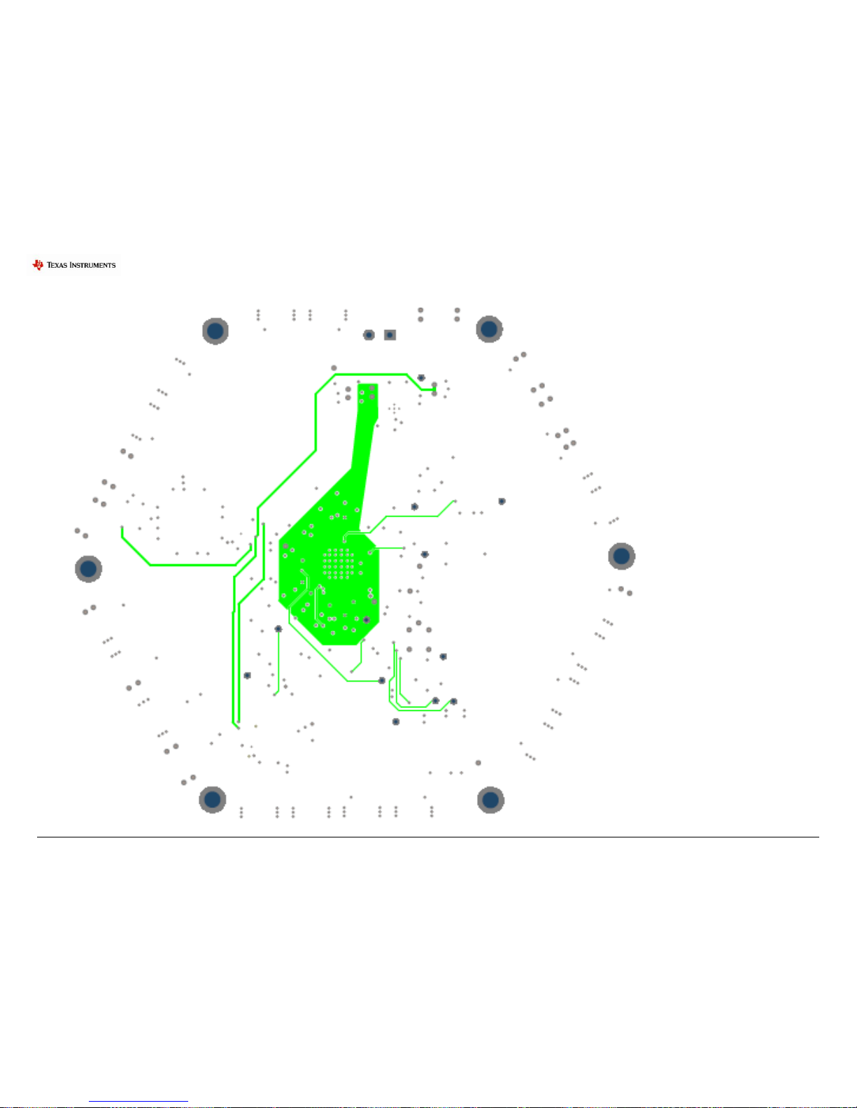
L M K 0 4 9 0 6 E V A L U A T I O N B O A R D O P E R A T I N G I N S T R U C T I O N S
SNAU126
57
Layer # 5 – Vcc Planes 2
Page 58

L M K 0 4 9 0 6 E V A L U A T I O N B O A R D O P E R A T I N G I N S T R U C T I O N S
SNAU126
58
Layer #6 – Bottom
Page 59
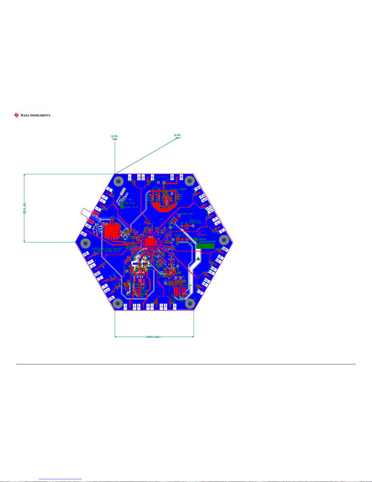
L M K 0 4 9 0 6 E V A L U A T I O N B O A R D O P E R A T I N G I N S T R U C T I O N S
SNAU126
59
Layers #1 and 6 – Top and Bottom (Composite)
Page 60

L M K 0 4 9 0 6 E V A L U A T I O N B O A R D O P E R A T I N G I N S T R U C T I O N S
60
Port
Address
LPT1
0x378
LPT2
0x278
LPT3
0x3BC
Appendix G: Properly Configuring LPT Port
When trying to solve any communications issue, it is most convenient to verify communication
by programming the POWERDOWN bit to confirm normal or low supply current consumption
of the evaluation board.
LPT Driver Loading
The parallel port must be configured for proper operation. To confirm that the LPT port driver is
successfully loading click “LPT/USB” “Check LPT.” If the driver properly loads then the
following message is displayed:
Figure 18: Successfully Opened LPT Driver
Successful loading of LPT driver does not mean LPT communications in CodeLoader are setup
properly. The proper LPT port must be selected and the LPT port must not be in an improper
mode.
The PC must be rebooted after install for LPT support to work properly.
Correct LPT Port/Address
To determine the correct LPT port in Windows, open the device manager (On Windows XP,
Start Settings Control Panel System Hardware tab Device Manager) and check
the LPT port under the Ports (COM & LPT) node of the tree. It can be helpful to confirm that
the LPT port is mapped to the expected port address, for instance to confirm that LPT1 is really
mapped to address 0x378. This can be checked by viewing the Properties of the LPT1 port and
viewing Resources tab to verify that the I/O Range starts at 0x378. CodeLoader expects the
traditional port mapping:
If a non-standard address is used, use the “Other” port address in CodeLoader and type in the
port address in hexadecimal. It is possible to change the port address in the computer‟s BIOS
settings. The port address can be set in CodeLoader in the Port Setup tab as shown in Figure 19.
SNAU126
Page 61

L M K 0 4 9 0 6 E V A L U A T I O N B O A R D O P E R A T I N G I N S T R U C T I O N S
61
Figure 19: Selecting the LPT Port Address
Correct LPT Mode
If communications are not working, then it is possible the LPT port mode is set improperly. It is
recommended to use the simple, Output-only mode of the LPT port. This can be set in the BIOS
of the computer. Common terms for this desired parallel port mode are “Normal,” “Output,” or
“AT.” It is possible to enter BIOS setup during the initial boot up sequence of the computer.
SNAU126
Page 62

L M K 0 4 9 0 6 E V A L U A T I O N B O A R D O P E R A T I N G I N S T R U C T I O N S
62
Appendix H: Troubleshooting Information
If the evaluation board is not behaving as expected, the most likely issues are…
1) Board communication issue
2) Incorrect Programming of the device
3) Setup Error
Refer to this checklist for a practical guide on identifying/exposing possible issues.
1) Confirm Communications
Refer to Appendix G: Properly Configuring LPT Port to troubleshoot this item.
Remember to load device with Ctrl+L.
2) Confirm PLL1 operation/locking
1) Program LD_MUX = “PLL1_R/2”
2) Confirm that LD pin output is half the expected phase detector frequency of PLL1.
i. If not, examine CLKin_SEL programming.
ii. If not, examine CLKin0_BUFTYPE / CLKin1_BUFTYPE.
iii. If not, examine PLL1 register R programming.
iv. If not, examine physical CLKin input.
3) Program LD_MUX = “PLL1_N /2”
4) Confirm that LD pin output is half the expected phase detector frequency of PLL1.
i. If not, examine PLL1 register N programming.
ii. If not, examine physical OSCin input.
Naturally, the output frequency of the above two items, PLL 1 R Divider/2 and PLL 1 N Divider
/2, on LD pin should be the same frequency.
5) Program LD_MUX = “PLL1_DLD”
6) Confirm the LD pin output is high.
i. If high, then PLL1 is locked, continue to PLL2 operation/locking.
7) If LD pin output is low, but the frequencies are the same, it is possible that excessive
leakage on Vtune pin is causing the digital lock detect to not activate. By default
PLL2 waits for the digital lock detect to go high before allowing PLL2 and the
integrated VCO to lock. Different VCXO models have different input leakage
specifications. High leakage, low PLL1 phase detector frequencies, and low PLL1
charge pump current settings can cause the PLL1 charge pump to operate longer than
the digital lock detect timeout which allows the device to lock, but prevents the
digital lock detect from activating.
i. Redesign PLL1 loop filter with higher phase detector frequency
ii. Redesign PLL1 loop filter with higher charge pump current
iii. Isolate VCXO tuning input from PLL1 charge pump with an op amp.
SNAU126
Page 63

L M K 0 4 9 0 6 E V A L U A T I O N B O A R D O P E R A T I N G I N S T R U C T I O N S
63
3) Confirm PLL2 operation/locking
1) Program LD_MUX = “PLL2_R/2”
2) Confirm that LD pin output is half the expected phase detector frequency of PLL2.
i. If not, examine PLL2_R programming.
ii. If not, examine physical OSCin input.
3) Program LD_MUX = “PLL2_N/2”
4) Confirm that LD pin output is half the expected phase detector frequency of PLL2.
i. If not, confirm OSCin_FREQ is programmed to OSCin frequency.
ii. If not, examine PLL2_N programming.
Naturally, the output frequency of the above two items should be the same frequency.
5) Program LD_MUX = “PLL2 DLD”
6) Confirm the LD pin output is high.
7) Program LD_MUX = “PLL1 & PLL2 DLD”
8) Confirm the LD pin output is high.
SNAU126
Page 64

L M K 0 4 9 0 6 E V A L U A T I O N B O A R D O P E R A T I N G I N S T R U C T I O N S
64
EVALUATION BOARD/KIT/MODULE (EVM) ADDITIONAL TERMS
Texas Instruments (TI) provides the enclosed Evaluation Board/Kit/Module (EVM) under the following
conditions:
The user assumes all responsibility and liability for proper and safe handling of the goods. Further, the
user indemnifies TI from all claims arising from the handling or use of the goods.
Should this evaluation board/kit not meet the specifications indicated in the User’s Guide, the board/ kit
may be returned within 30 days from the date of delivery for a full refund. THE FOREGOING LIMITED
WARRANTY IS THE EXCLUSIVE WARRANTY MADE BY SELLER TO BUYER AND IS IN LIEU OF ALL
OTHER WARRANTIES, EXPRESSED, IMPLIED, OR STATUTORY, INCLUDING ANY WARRANTY OF
MERCHANTABILITY OR FITNESS FOR ANY PARTICULAR PURPOSE. EXCEPT TO THE EXTENT OF
THE INDEMNITY SET FORTH ABOVE, NEITHER PARTY SHALL BE LIABLE TO THE OTHER FOR
ANY INDIRECT, SPECIAL, INCIDENTAL, OR CONSEQUENTIAL DAMAGES.
Please read the User's Guide and, specifically, the Warnings and Restrictions notice in the User's Guide
prior to handling the product. This notice contains important safety information about temperatures and
voltages. For additional information on TI's environmental and/or safety programs, please visit
www.ti.com/esh or contact TI.
No license is granted under any patent right or other intellectual property right of TI covering or relating to
any machine, process, or combination in which such TI products or services might be or are used. TI
currently deals with a variety of customers for products, and therefore our arrangement with the user is
not exclusive. TI assumes no liability for applications assistance, customer product design, software
performance, or infringement of patents or services described herein.
Mailing Address: Texas Instruments Post Office Box 655303 Dallas, Texas 75265
Copyright 2012, Texas Instruments Incorporated
REGULATORY COMPLIANCE INFORMATION
As noted in the EVM User’s Guide and/or EVM itself, this EVM and/or accompanying hardware may or
may not be subject to the Federal Communications Commission (FCC) and Industry Canada (IC) rules.
For EVMs not subject to the above rules, this evaluation board/kit/module is intended for use for
ENGINEERING DEVELOPMENT, DEMONSTRATION OR EVALUATION PURPOSES ONLY and is not
considered by TI to be a finished end product fit for general consumer use. It generates, uses, and can
radiate radio frequency energy and has not been tested for compliance with the limits of computing
devices pursuant to part 15 of FCC or ICES-003 rules, which are designed to provide reasonable
protection against radio frequency interference. Operation of the equipment may cause interference with
radio communications, in which case the user at his own expense will be required to take whatever
measures may be required to correct this interference.
General Statement for EVMs including a radio
User Power/Frequency Use Obligations: This radio is intended for development/professional use only in
legally allocated frequency and power limits. Any use of radio frequencies and/or power availability of this
EVM and its development application(s) must comply with local laws governing radio spectrum allocation
and power limits for this evaluation module. It is the user’s sole responsibility to only operate this radio in
legally acceptable frequency space and within legally mandated power limitations. Any exceptions to this
SNAU126
Page 65

L M K 0 4 9 0 6 E V A L U A T I O N B O A R D O P E R A T I N G I N S T R U C T I O N S
65
is strictly prohibited and unauthorized by Texas Instruments unless user has obtained appropriate
experimental/development licenses from local regulatory authorities, which is responsibility of user
including its acceptable authorization.
For EVMs annotated as FCC – FEDERAL COMMUNICATIONS COMMISSION Part 15 Compliant
Caution
This device complies with part 15 of the FCC Rules. Operation is subject to the following two conditions:
(1) This device may not cause harmful interference, and (2) this device must accept any interference
received, including interference that may cause undesired operation.
Changes or modifications not expressly approved by the party responsible for compliance could void the
user's authority to operate the equipment.
FCC Interference Statement for Class A EVM devices
This equipment has been tested and found to comply with the limits for a Class A digital device, pursuant
to part 15 of the FCC Rules. These limits are designed to provide reasonable protection against harmful
interference when the equipment is operated in a commercial environment. This equipment generates,
uses, and can radiate radio frequency energy and, if not installed and used in accordance with the
instruction manual, may cause harmful interference to radio communications. Operation of this equipment
in a residential area is likely to cause harmful interference in which case the user will be required to
correct the interference at his own expense.
FCC Interference Statement for Class B EVM devices
This equipment has been tested and found to comply with the limits for a Class B digital device, pursuant
to part 15 of the FCC Rules. These limits are designed to provide reasonable protection against harmful
interference in a residential installation. This equipment generates, uses and can radiate radio frequency
energy and, if not installed and used in accordance with the instructions, may cause harmful interference
to radio communications. However, there is no guarantee that interference will not occur in a particular
installation. If this equipment does cause harmful interference to radio or television reception, which can
be determined by turning the equipment off and on, the user is encouraged to try to correct the
interference by one or more of the following measures:
Reorient or relocate the receiving antenna.
Increase the separation between the equipment and receiver.
Connect the equipment into an outlet on a circuit different from that to which the receiver is
connected.
Consult the dealer or an experienced radio/TV technician for help.
For EVMs annotated as IC – INDUSTRY CANADA Compliant
This Class A or B digital apparatus complies with Canadian ICES-003.
Changes or modifications not expressly approved by the party responsible for compliance could void the
user’s authority to operate the equipment.
Concerning EVMs including radio transmitters
SNAU126
Page 66

L M K 0 4 9 0 6 E V A L U A T I O N B O A R D O P E R A T I N G I N S T R U C T I O N S
66
This device complies with Industry Canada licence-exempt RSS standard(s). Operation is subject to the
following two conditions: (1) this device may not cause interference, and (2) this device must accept any
interference, including interference that may cause undesired operation of the device.
Concerning EVMs including detachable antennas
Under Industry Canada regulations, this radio transmitter may only operate using an antenna of a type
and maximum (or lesser) gain approved for the transmitter by Industry Canada. To reduce potential radio
interference to other users, the antenna type and its gain should be so chosen that the equivalent
isotropically radiated power (e.i.r.p.) is not more than that necessary for successful communication.
This radio transmitter has been approved by Industry Canada to operate with the antenna types listed in
the user guide with the maximum permissible gain and required antenna impedance for each antenna
type indicated. Antenna types not included in this list, having a gain greater than the maximum gain
indicated for that type, are strictly prohibited for use with this device.
~
Cet appareil numérique de la classe A ou B est conforme à la norme NMB-003 du Canada.
Les changements ou les modifications pas expressément approuvés par la partie responsable de la
conformité ont pu vider l’autorité de l'utilisateur pour actionner l'équipement.
Concernant les EVMs avec appareils radio
Le présent appareil est conforme aux CNR d'Industrie Canada applicables aux appareils radio exempts
de licence. L'exploitation est autorisée aux deux conditions suivantes : (1) l'appareil ne doit pas produire
de brouillage, et (2) l'utilisateur de l'appareil doit accepter tout brouillage radioélectrique subi, même si le
brouillage est susceptible d'en compromettre le fonctionnement.
Concernant les EVMs avec antennes détachables
Conformément à la réglementation d'Industrie Canada, le présent émetteur radio peut fonctionner avec
une antenne d'un type et d'un gain maximal (ou inférieur) approuvé pour l'émetteur par Industrie Canada.
Dans le but de réduire les risques de brouillage radioélectrique à l'intention des autres utilisateurs, il faut
choisir le type d'antenne et son gain de sorte que la puissance isotrope rayonnée équivalente (p.i.r.e.) ne
dépasse pas l'intensité nécessaire à l'établissement d'une communication satisfaisante.
Le présent émetteur radio a été approuvé par Industrie Canada pour fonctionner avec les types d'antenne
énumérés dans le manuel d’usage et ayant un gain admissible maximal et l'impédance requise pour
chaque type d'antenne. Les types d'antenne non inclus dans cette liste, ou dont le gain est supérieur au
gain maximal indiqué, sont strictement interdits pour l'exploitation de l'émetteur.
Important Notice for Users of this Product in Japan】
This development kit is NOT certified as Confirming to Technical Regulations of
Radio Law of Japan!
If you use this product in Japan, you are required by Radio Law of Japan to follow the instructions below
with respect to this product:
(1) Use this product in a shielded room or any other test facility as defined in the notification #173
issued by Ministry of Internal Affairs and Communications on March 28, 2006, based on Sub-section 1.1
of Article 6 of the Ministry’s Rule for Enforcement of Radio Law of Japan,
SNAU126
Page 67

L M K 0 4 9 0 6 E V A L U A T I O N B O A R D O P E R A T I N G I N S T R U C T I O N S
67
(2) Use this product only after you obtained the license of Test Radio Station as provided in Radio
Law of Japan with respect to this product, or
(3) Use of this product only after you obtained the Technical Regulations Conformity Certification
as provided in Radio Law of Japan with respect to this product.
Also, please do not transfer this product, unless you give the same notice above to the transferee.
Please note that if you could not follow the instructions above, you will be subject to penalties of Radio
Law of Japan.
Texas Instruments Japan Limited
(address) 24-1, Nishi-Shinjuku 6 chome, Shinjukku-ku, Tokyo, Japan
http://www.tij.co.jp
【ご使用にあたっての注意】
本開発キットは技術基準適合証明を受けておりません。
本製品のご使用に際しては、電波法遵守のため、以下のいずれかの措置を取っていただく必要がありま
すのでご注意ください。
(1)電波法施行規則第 6 条第 1 項第 1 号に基づく平成 18 年 3 月 28 日総務省告示第 173 号で
定められた電波暗室等の試験設備でご使用いただく。
(2)実験局の免許を取得後ご使用いただく。
(3)技術基準適合証明を取得後ご使用いただく。
なお、本製品は、上記の「ご使用にあたっての注意」を譲渡先、移転先に通知しない限り、譲渡、移転
できないものとします。
上記を遵守頂けない場合は、電波法の罰則が適用される可能性があることをご留意ください。
日本テキサス・インスツルメンツ株式会社
東京都新宿区西新宿6丁目24番1号
西新宿三井ビル
http://www.tij.co.jp
SNAU126
Page 68

L M K 0 4 9 0 6 E V A L U A T I O N B O A R D O P E R A T I N G I N S T R U C T I O N S
68
EVALUATION BOARD/KIT/MODULE (EVM)
WARNINGS, RESTRICTIONS AND DISCLAIMERS
For Feasibility Evaluation Only, in Laboratory/Development Environments. Unless otherwise
indicated, this EVM is not a finished electrical equipment and not intended for consumer use. It is
intended solely for use for preliminary feasibility evaluation in laboratory/development environments by
technically qualified electronics experts who are familiar with the dangers and application risks associated
with handling electrical mechanical components, systems and subsystems. It should not be used as all or
part of a finished end product.
Your Sole Responsibility and Risk. You acknowledge, represent and agree that:
1. You have unique knowledge concerning Federal, State and local regulatory requirements (including
but not limited to Food and Drug Administration regulations, if applicable) which relate to your
products and which relate to your use (and/or that of your employees, affiliates, contractors or
designees) of the EVM for evaluation, testing and other purposes.
2. You have full and exclusive responsibility to assure the safety and compliance of your products with
all such laws and other applicable regulatory requirements, and also to assure the safety of any
activities to be conducted by you and/or your employees, affiliates, contractors or designees, using
the EVM. Further, you are responsible to assure that any interfaces (electronic and/or mechanical)
between the EVM and any human body are designed with suitable isolation and means to safely limit
accessible leakage currents to minimize the risk of electrical shock hazard.
3. You will employ reasonable safeguards to ensure that your use of the EVM will not result in any
property damage, injury or death, even if the EVM should fail to perform as described or expected.
4. You will take care of proper disposal and recycling of the EVM’s electronic components and packing
materials.
Certain Instructions. It is important to operate this EVM within TI’s recommended specifications and
environmental considerations per the user guidelines. Exceeding the specified EVM ratings (including but
not limited to input and output voltage, current, power, and environmental ranges) may cause property
damage, personal injury or death. If there are questions concerning these ratings please contact a TI field
representative prior to connecting interface electronics including input power and intended loads. Any
loads applied outside of the specified output range may result in unintended and/or inaccurate operation
and/or possible permanent damage to the EVM and/or interface electronics. Please consult the EVM
User's Guide prior to connecting any load to the EVM output. If there is uncertainty as to the load
specification, please contact a TI field representative. During normal operation, some circuit components
may have case temperatures greater than 60oC as long as the input and output are maintained at a
normal ambient operating temperature. These components include but are not limited to linear regulators,
switching transistors, pass transistors, and current sense resistors which can be identified using the EVM
schematic located in the EVM User's Guide. When placing measurement probes near these devices
during normal operation, please be aware that these devices may be very warm to the touch. As with all
electronic evaluation tools, only qualified personnel knowledgeable in electronic measurement and
diagnostics normally found in development environments should use these EVMs.
Agreement to Defend, Indemnify and Hold Harmless. You agree to defend, indemnify and hold TI, its
licensors and their representatives harmless from and against any and all claims, damages, losses,
expenses, costs and liabilities (collectively, "Claims") arising out of or in connection with any use of the
EVM that is not in accordance with the terms of the agreement. This obligation shall apply whether
Claims arise under law of tort or contract or any other legal theory, and even if the EVM fails to perform as
described or expected.
SNAU126
Page 69

L M K 0 4 9 0 6 E V A L U A T I O N B O A R D O P E R A T I N G I N S T R U C T I O N S
69
Safety-Critical or Life-Critical Applications. If you intend to evaluate the components for possible use
in safety critical applications (such as life support) where a failure of the TI product would reasonably be
expected to cause severe personal injury or death, such as devices which are classified as FDA Class III
or similar classification, then you must specifically notify TI of such intent and enter into a separate
Assurance and Indemnity Agreement.
IMPORTANT NOTICE
Texas Instruments Incorporated and its subsidiaries (TI) reserve the right to make corrections,
modifications, enhancements, improvements, and other changes to its products and services at any time
and to discontinue any product or service without notice. Customers should obtain the latest relevant
information before placing orders and should verify that such information is current and complete. All
products are sold subject to TI’s terms and conditions of sale supplied at the time of order
acknowledgment.
TI warrants performance of its hardware products to the specifications applicable at the time of sale in
accordance with TI’s standard warranty. Testing and other quality control techniques are used to the
extent TI deems necessary to support this warranty. Except where mandated by government
requirements, testing of all parameters of each product is not necessarily performed.
TI assumes no liability for applications assistance or customer product design. Customers are
responsible for their products and applications using TI components. To minimize the risks associated
with customer products and applications, customers should provide adequate design and operating
safeguards.
TI does not warrant or represent that any license, either express or implied, is granted under any TI
patent right, copyright, mask work right, or other TI intellectual property right relating to any combination,
machine, or process in which TI products or services are used. Information published by TI regarding
third-party products or services does not constitute a license from TI to use such products or services or
a warranty or endorsement thereof. Use of such information may require a license from a third party
under the patents or other intellectual property of the third party, or a license from TI under the patents or
other intellectual property of TI. Reproduction of information in TI data books or data sheets is
permissible only if reproduction is without alteration and is accompanied by all associated warranties,
conditions, limitations, and notices.
Reproduction of this information with alteration is an unfair and deceptive business practice. TI is not
responsible or liable for such altered documentation. Resale of TI products or services with statements
different from or beyond the parameters stated by TI for that product or service voids all express and any
implied warranties for the associated TI product or service and is an unfair and deceptive business
practice. TI is not responsible or liable for any such statements.
TI products are not authorized for use in safety-critical applications (such as life support) where a failure
of the TI product would reasonably be expected to cause severe personal injury or death, unless officers
of the parties have executed an agreement specifically governing such use. Buyers represent that they
have all necessary expertise in the safety and regulatory ramifications of their applications, and
acknowledge and agree that they are solely responsible for all legal, regulatory and safety-related
requirements concerning their products and any use of TI products in such safety-critical applications,
notwithstanding any applications-related information or support that may be provided by TI. Further,
Buyers must fully indemnify TI and its representatives against any damages arising out of the use of TI
products in such safety-critical applications.
TI products are neither designed nor intended for use in military/aerospace applications or environments
unless the TI products are specifically designated by TI as military-grade or "enhanced plastic." Only
products designated by TI as military-grade meet military specifications. Buyers acknowledge and agree
that any such use of TI products which TI has not designated as military-grade is solely at the Buyer's
risk, and that they are solely responsible for compliance with all legal and regulatory requirements in
connection with such use.
TI products are neither designed nor intended for use in automotive applications or environments unless
the specific TI products are designated by TI as compliant with ISO/TS 16949 requirements. Buyers
acknowledge and agree that, if they use any non-designated products in automotive applications, TI will
not be responsible for any failure to meet such requirements.
Following are URLs where you can obtain information on other Texas Instruments products and
application solutions:
Products Applications
SNAU126
Page 70

L M K 0 4 9 0 6 E V A L U A T I O N B O A R D O P E R A T I N G I N S T R U C T I O N S
70
Amplifiers amplifier.ti.com Audio
www.ti.com/audio
Data Converters dataconverter.ti.com Automotive
www.ti.com/automotive
DSP dsp.ti.com Broadband
www.ti.com/broadband
Interface interface.ti.com Digital Control
www.ti.com/digitalcontrol
Logic logic.ti.com Military
www.ti.com/military
Power Mgmt power.ti.com Optical Networking
www.ti.com/opticalnetwork
Microcontrollers microcontroller.ti.com Security
www.ti.com/security
RFID www.ti-rfid.com Telephony
www.ti.com/telephony
Low Power www.ti.com/lpw Video & Imaging
www.ti.com/video
Wireless Wireless
www.ti.com/wireless
Mailing Address: Texas Instruments, Post Office Box 655303, Dallas, Texas 75265
Copyright © 2007, Texas Instruments Incorporated
SNAU126
Page 71

Mouser Electronics
Authorized Distributor
Click to View Pricing, Inventory, Delivery & Lifecycle Information:
Texas Instruments:
LMK04906BEVAL/NOPB
 Loading...