

Page 1
V104
™
C/C++ Programmable 16-bit Microprocessor Module
Based on the NEC V25, with a PC/104 Bus
Technical Manual
1950 5th Street, Davis, CA 95616, USA
Tel: 530-758-0180 Fax: 530-758-0181
Email:
sales@tern.com http://www.tern.com
Page 2

COPYRIGHT
V104, A-Drive, V25-Engine, VE232, NT-Kit, and ACTF are trademarks of TERN, Inc.
V25 is a Trademark of NEC Electronics Inc.
Borland C/C++ is a trademark of Borland International.
Microsoft, MS-DOS, Windows, Windows95, and Windows98 are trademarks of
Microsoft Corporation.
IBM is a trademark of International Business Machines Corporation.
Version 3.00
October 29, 2010
No part of this document may be copied or reproduced in any form or by any means
without the prior written consent of TERN, Inc.
© 1995-2010
1950 5th Street, Davis, CA 95616, USA
Tel: 530-758-0180 Fax: 530-758-0181
Email: sales@tern.com http://www.tern.com
Important Notice
TERN is developing complex, high technology integration systems. These systems are
integrated with software and hardware that are not 100% defect free. TERN products are
not designed, intended, authorized, or warranted to be suitable for use in life-support
applications, devices, or systems, or in other critical applications. TERN and the Buyer
agree that TERN will not be liable for incidental or consequential damages arising from
the use of TERN products. It is the Buyer's responsibility to protect life and property
against incidental failure.
TERN reserves the right to make changes and improvements to its products without
providing notice.
Temperature readings for controllers are based on the results of limited sample tests; they
are provided for design reference use only.
Page 3

V104 Chapter 1: Introduction
1-1
Chapter 1: Introduction
1.1 Functional Description
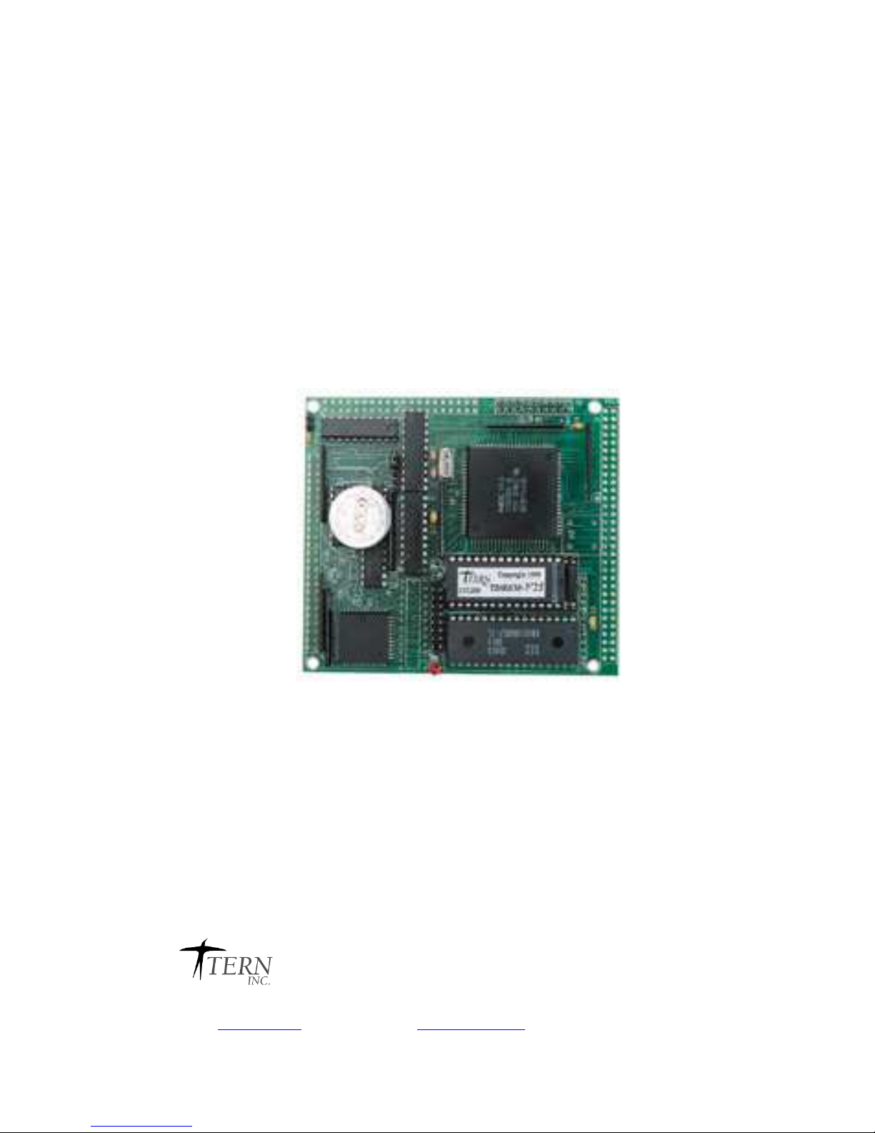
The V104 from TERN is a low cost, high performance, C/C++ programmable, 16-bit microprocessor core
module. It is designed for embedded applications that require compactness, low power consumption, and
high reliability. The V104 can be integrated into an OEM product as a processor core component. It also
can be used to build a smart sensor, or as a node in a distributed microprocessor system.
Int SRAM
(512 bytes)
Ser0
Ser1
Time Base Counter
16-Bit Timers (2)
Port T with 8 Comparators
Ext. Interrupts (5)
16-bit counter/DMA (2)
Digital I/O Ports (3)
HLDRQ/AK
MAX691
Supervisor
EEPROM
up to 2K
SCL
SDA
P00P01
P03
NMI
RSTPFO
VRAM
V104
16-bit C/C++
Controller
Data
Addr
Cntl
*
EPROM/Flash
(0xf0000-0xfffff, memory)
SRAM
(0-0x7ffff, memory)
UART SCC2691
(0xc000-0xffff, I/O)
RTC72421
(0x8000-0xbfff, I/O)
*
*
U2
U3
U1
U8
U4
U6
U7
HWD
/RESET
V25
CPU
80x86/8088
Compatible
TLC2543
U10
PPI 82c55
bi-directional 24 I/Os
11 ch. 12-bit ADC
INT1/INT2/NMI
4-bit ADC
Analog or
Digital
I/O
TTL inputs
MAX537
4 ch. 12-bit DAC
U12
PC/104 bus
LCD interface
Figure 1.1 Functional block diagram of the V104
Measuring 4.0 x 3.5 x 0.5 inches, the V104 offers a complete C/C++ programmable computer system with a
16-bit high performance CPU (NEC V25) and operates at 8 MHz with zero-wait-states. Optional features
include up to 512K EPROM/Flash and up to 512K battery-backed SRAM. A 512-byte serial EEPROM is
included on-board. An optional real-time clock provides information on the year, month, date, hour, minute,
second, and 1/64 second, and an interrupt signal.
Two DMA-driven serial ports from the NEC V25 support high-speed, reliable serial communication at a
rate of up to 115,200 baud. An optional UART SCC2691 may be added in order to have a third UART onboard. All three serial ports support 8-bit and 9-bit communication.
The optional 12-bit ADC has 11 channels of analog inputs with sample-and-hold and a high-impedance
reference input (2.5-5V) that facilitate ratiometric conversion, scaling, and isolation of analog circuitry from
logic and supply noise.
The optional 4-channel 12-bit DAC voltage outputs (0V to 2.5V) are internally buffered by precision unitygain followers with a typical slew rate of 3V/µs with 5 KΩ load. It must be installed with a precision
reference voltage (included) and requires a -5V external power supply.
Page 4

V104 Chapter 1: Introduction
1-2
A 16-pin LCD interface header supports various types of LCD modules. By default, the LCD select line is
active high.
The optional VE232 provides regulated 5V power and RS232/RS485 drivers for the V104. The V104 can
also be installed on the A-Drive to provide regulated 5V power and RS232/RS485 drivers. TERN also
offers custom hardware and software design, based on the V104 or other TERN controllers.
1.2 Features
Standard Features
• Dimensions: 4.0 x 3.5 x 0.5 inches
• Power consumption: 100 mA at 5V, 40 mA standby (with standard parts)
• Low power version: 60 mA full speed, 5 mA standby (with low power parts)
• Power Input: +5V regulated DC without VE232
• +9V to +12V unregulated DC with VE232
• 16-bit CPU (NEC V25), 8 MHz, Intel 80x86 compatible, C/C++ programmable
• ROM and SRAM up to 1MB, 512-byte EEPROM (or up to 2KB) and 256 bytes built-in-CPU
SRAM
• Five external interrupts
• 24 bi-directional digital I/O lines
• 8 comparator inputs
• Two 16-bit timers, one 16-bit time base counter
• Two 16-bit counters or DMA. The counter can count external signal rising edges up to 500 KHz
• Two high speed serial ports from the V25 CPU
• Supervisor chip (691) for power failure, reset and watchdog
• LCD interface
Optional Features
:
• 32KB, 128KB, or 512KB SRAM
• 11 channels of 12-bit ADC, sample rate up to 10 KHz
• 4 channels of 12-bit DAC (MAX 537) with 2.5V Reference
• SCC2691 UART (on-board) supports 8-bit or 9-bit networking
• Real-time clock RTC72423, lithium coin battery
• VE232 add-on board for regulated 5V power & RS232/RS485 drivers
• PC104 64-pin connector
• 16x2 character LCD
Figure 1.2 VE232 interface board
Page 5
V104 Chapter 1: Introduction
1-3
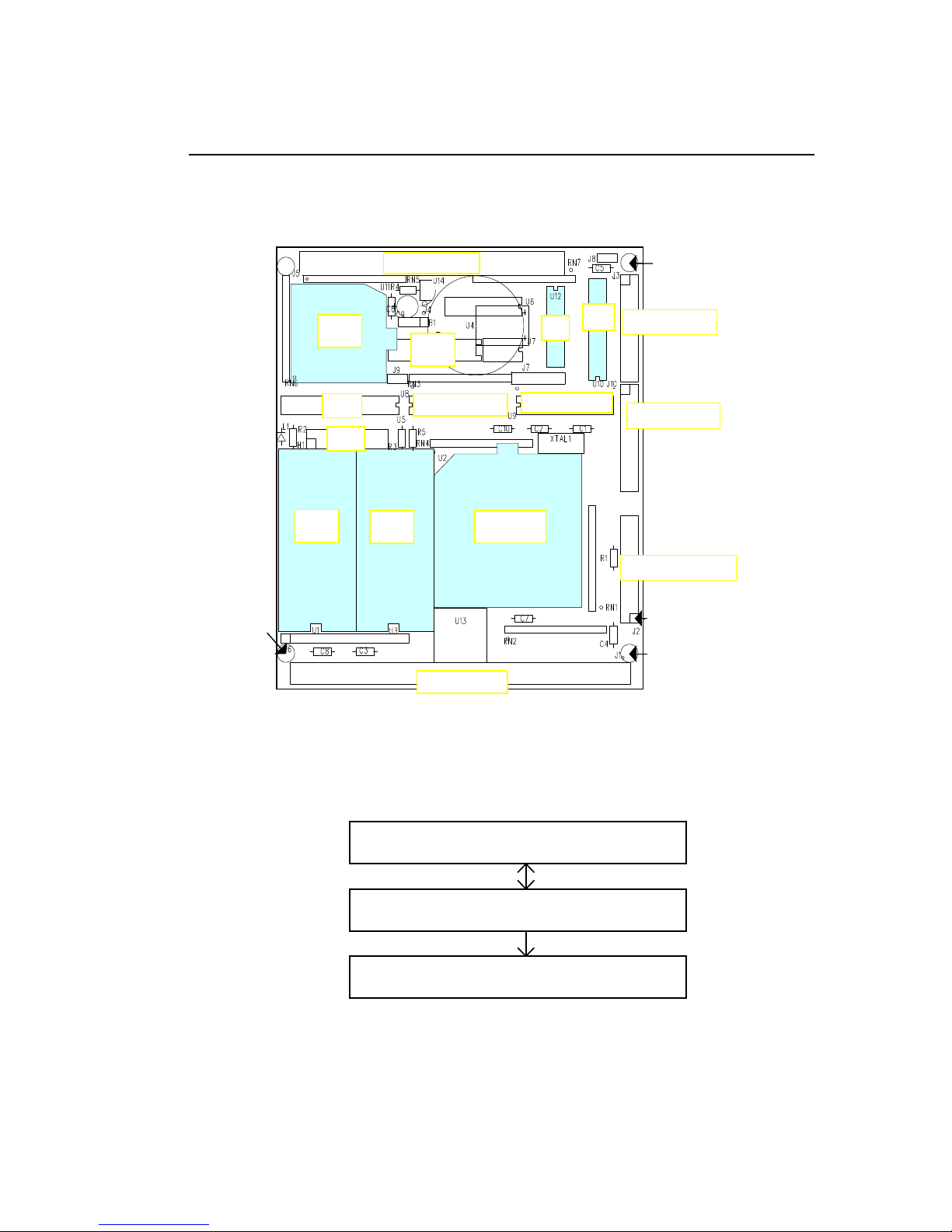
1.3 Physical Description
The physical layout of the V104 is shown in Figure 1.3.
PC/104 Bus
ROM V25 CPU
RAM
LCD
PPI
SCC
AD
DA
RTC
J3 AD/DA header
V25 Ports
VE232 interface
PAL V104P1000
PAL V104P000
J5 24 I/O lines
Figure 1.3 Physical layout of the V104
1.4 V104 Programming Overview
Development of application software for the V104 consists of three easy steps, as shown in the block
diagram below.
Replace Debug ROM, project is complete.
STEP 3
Test V104 in the field, away from PC.STEP 2
Application program resides in the battery-backed SRAM.
Debug and run application with remote Debugger.
STEP 1 Serial link PC and V104, program in C/C++.
Burn application ROM.
You can program the V104 from your PC via serial link with an RS232 interface. Your C/C++ program can
be remotely debugged over the serial link at a rate of 115,000 baud. The C/C++ Evaluation Kit (EV) or
Development Kit (DV) from TERN provides a Borland C/C++ compiler, TASM, LOC31, Turbo Remote
Page 6

V104 Chapter 1: Introduction
1-4
Debugger, I/O driver libraries, sample programs, and batch files. These kits also include a DEBUG ROM
(TDREM_V25) to communicate with Turbo Debugger, a DB9-IDE10 (PC-V25) serial cable to connect the
controller to the PC, and a 9-volt wall transformer. See your Evaluation/Development Kit Technical Manual
for more information on these kits.
After you debug your program, you can test run the V104 in the field, away from the PC, by changing a
single jumper, with the application program residing in the battery-backed SRAM. When the field test is
complete, application ROMs can be produced to replace the DEBUG ROM. The .HEX or .BIN file can be
easily generated with the makefile provided. You may also use the DV Kit or ACTF Kit to download your
application code to on-board Flash.
The three steps in the development of a C/C++ application program are explained in detail below.
1.4.1 Step 1
STEP 1: Debugging
• Write your C/C++ application program in C/C++.
• Connect your controller to your PC via the PC-V25 serial link cable.
• Use the batch file m.bat to compile, link, and locate, or use t.bat to compile, link locate, download,
and debug your C/C++ application program.
VE232 + V104
DC power jack
on the VE232
DC +9V 300 mA
Wall transformer
Center Negative
PC-V25 Cable
PC
Figure 1.4 Step 1 connections for the V104
Page 7

V104 Chapter 1: Introduction
1-5
1.4.2 Step 2
STEP 2: Standalone Field Test.
• Set the jumper on J10 pins 19 and 20 on the V104 (Figure 1.5).
• At power-on or reset, if J10 pin 19 (P02) is low, the CPU will run the code that resides in the battery-
backed SRAM.
• If a jumper is on J10 pins 19-20 at power-on or reset, the V104 will operate in Step Two mode. If the
jumper is off J10 pins 19-20 at power-on or reset, the V104 will operate in Step One mode. The status
of J10 pin 19 (signal P02 of the NEC V25) is only checked at power-on or at reset.
PC/104 Bus
ROM
V25 CPU RAM
LCD
PPI
SCC
AD
DA
RTC
0, 0
3.5x4.0
pin 20=GND, pin 19=P02
Step 2 jumper
Figure 1.5 Location of Step 2 jumper on the V104
1.4.3 Step 3
STEP 3: Generate the application .BIN or .HEX file, make production ROMs or download your program to
FLASH via ACTF.
• If you are happy with your Step Two test, you can go back to your PC to generate your application
ROM to replace the DEBUG ROM (TDREM_V25). You need to change DEBUG=1 to DEBUG=0 in
the makefile.
You need to have the DV Kit to complete Step Three.
Please refer to the Tutorial of the Technical Manual of the EV/DV Kit for further details on programming
the V104.
1.5 VE232
The VE232 is an interface board for the V104 that provides regulated +5V DC power and RS232/485
drivers. It converts TTL signals to and from RS232 signals. You do not need the VE232 if you are using
the V104 installed on another TERN controller such as the P300, PC-Co, MotionC, PowerDrive, or
SensorWatch.
The VE232, shown in Figure 1.6, measures 2.3 x 1.57 inches. A wall transformer (9V, 300 mA) with a
center negative DC plug (Ø=2.0 mm) should be used to power the V104 via the VE232. The VE232
Page 8
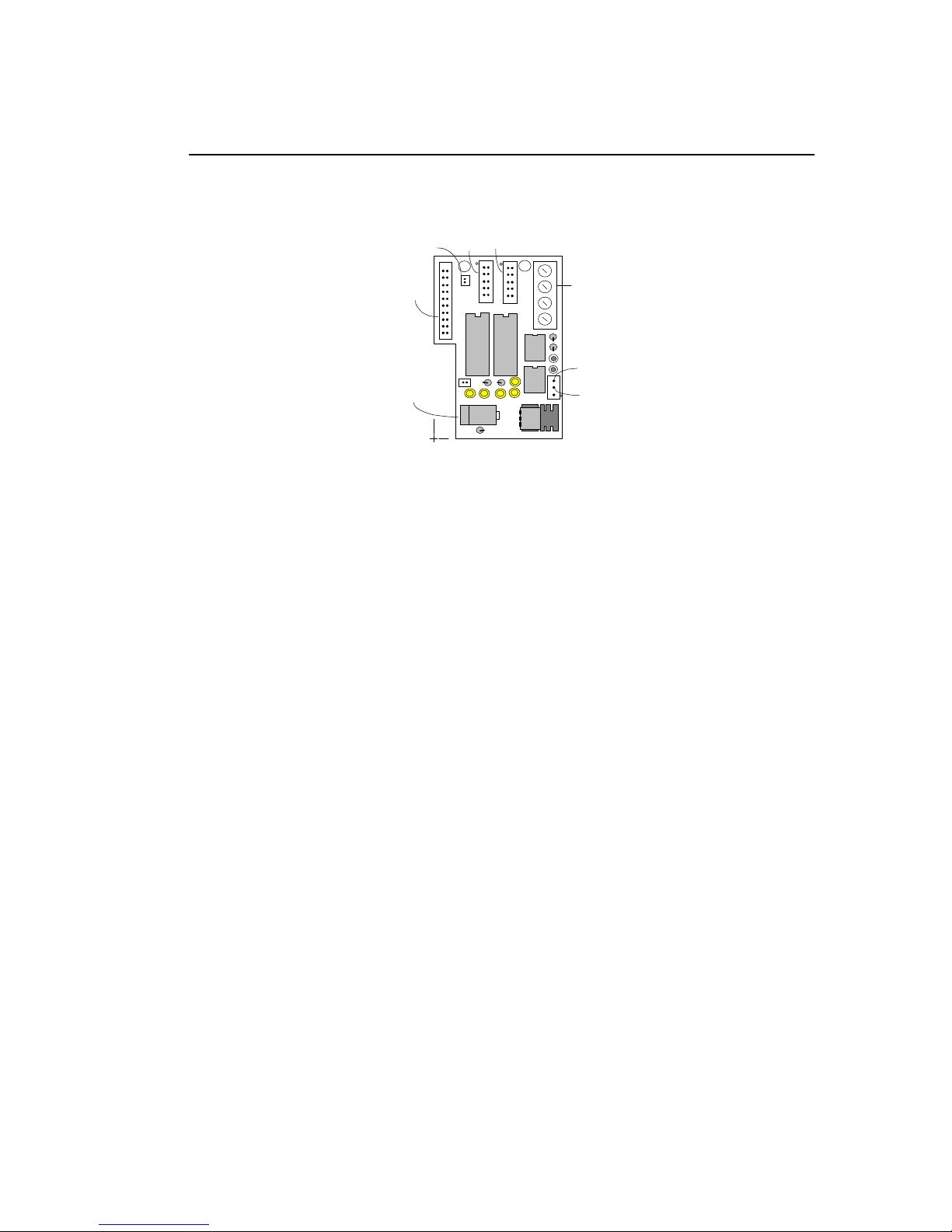
V104 Chapter 1: Introduction
1-6
connects to V104 via H1 (2x10 header). SER0 (J2) and SER1 (J3) on the VE232 are 2x5-pin headers for
serial ports SER0 and SER1. SER0 is the default programming port.
power jack
VE232
DC
0, 0
1.57, 2.30
(inch)
H1
H3 pin 3
J6
1488
U6
485
U5
7662
U4
1489
U1
J1
H2
SER1
J3
SER0
J2
H3 pin 2
Figure 1.6 The VE232, an interface card for the V104
For further information on the VE232, please refer to Appendix B and to the VE232 schematic at the end of
this manual.
1.6 Minimum Requirements for V104 System Development
1.6.1 Minimum Hardware Requirements
• PC or PC-compatible computer with serial COMx port that supports 115,200 baud
• V104 controller with DEBUG ROM TDREM_V25
• VE232 interface board *
• DB9-IDE10 (PC-V25) serial cable (RS232; DB9 connector for PC COM port and IDC 2x5 connector
for controller)
• center negative wall transformer (+9V 500 mA)
* NOTE: the VE232 is not needed if you are using the V104 installed on another controller
1.6.2 Minimum Software Requirements
• TERN EV/DV Kit installation diskettes
• PC software environment: DOS, Windows 3.1, Windows95, or Windows98
The C/C++ Evaluation Kit (EV) and C/C++ Development Kit (DV) are available from TERN. The EV Kit
is a limited-functionality version of the DV Kit. With the EV Kit, you can program and debug the V104 in
Step One and Step Two, but you cannot run Step Three. In order to generate an application ROM/Flash file,
make production version ROMs, and complete the project, you will need the Development Kit (DV).
Page 9
V104 Chapter 2: Installation
2-1
Chapter 2: Installation
2.1 Software Installation
Please refer to the Technical manual for the “C/C++ Development Kit and Evaluation Kit for TERN
Embedded Microcontrollers” for information on installing software.
The README.TXT file on the TERN EV/DV disk contains important information about the installation
and evaluation of TERN controllers.
2.2 Hardware Installation
Hardware installation for the V104 consists primarily of connecting the microcontroller to your PC. For the
V104, the VE232 must be used to supply regulated power and RS232 drivers to the V104. If you are using
the V104 installed on another controller, please refer to the technical manual for that controller for
installation information.
2.2.1 Connecting the VE232 to the V104
VE232
H1
J2
PC/104 Bus
ROM
V25 CPU RAM
LCD
PPI
SCC
AD
DA
RTC
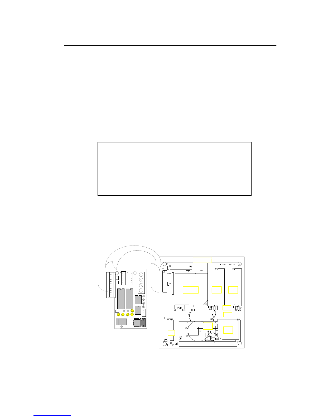
Figure 2.1 Before installing the VE232 on the V104
Overview
• Install VE232 (if applicable):
H1 connector of VE232 installs on J2 of the V104
• Connect PC-V25 cable:
For debugging (Step One), place connector on SER0 with red edge
of cable at pin 1
• Connect wall transformer:
Connect 9V wall transformer to power and plug into power jack
Page 10
V104 Chapter 2: Installation
2-2
VE232
Figure 2.2 After installing the VE232 on the V104
Install the VE232 interface with the H1 (10x2) socket connector on the upper half of the J2 (dual row
header) of the V104. Figure 2.1 and Figure 2.2 show the VE232 and the V104 before and after installation.
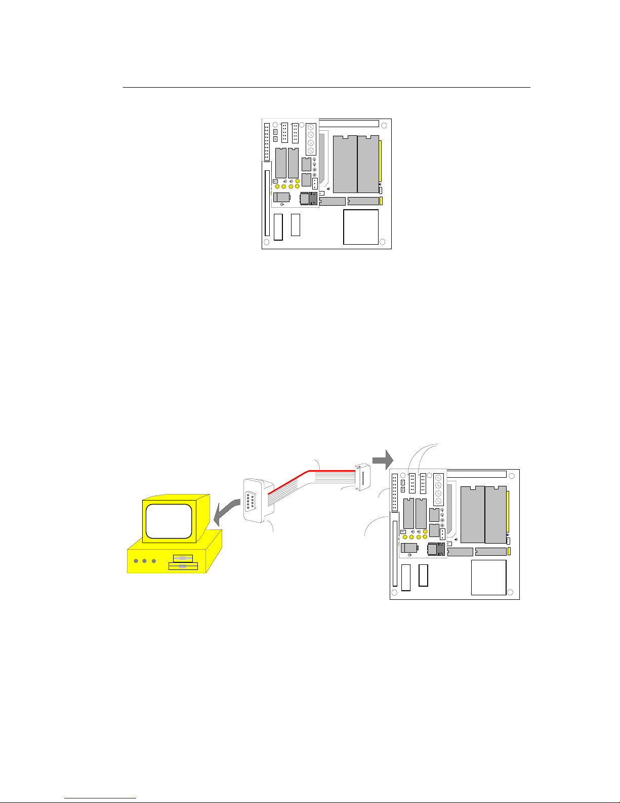
2.2.2 Connecting the V104 to the PC
The following diagram (Figure 2.3) illustrates the connection between the V104, VE232, and the PC. The
V104 is linked to the PC via a serial cable (PC-V25).
The TDREM_V25 DEBUG ROM communicates through SER0 by default. Install the 5x2 IDC connector
on the SER0 header of the VE232. IMPORTANT: Note that the red side of the cable must point to pin 1
of the VE232 H1 header. The DB9 connector should be connected to one of your PC's COM Ports (COM1
or COM2).
V104
VE232
SER0
SER1
or COM2
To COM1
Indication of pin 1 of
To SER0
or SER1
PC
Red side of serial
cable corresponds
SER0/SER1
headers for SER0 & SER1
to pin 1 of headers for
H1 on
VE232
J2 of V104
9-pin
connector
IDE
connector
VE232
Figure 2.3 Connecting the V104 and VE232 to the PC
Page 11
V104 Chapter 2: Installation
2-3
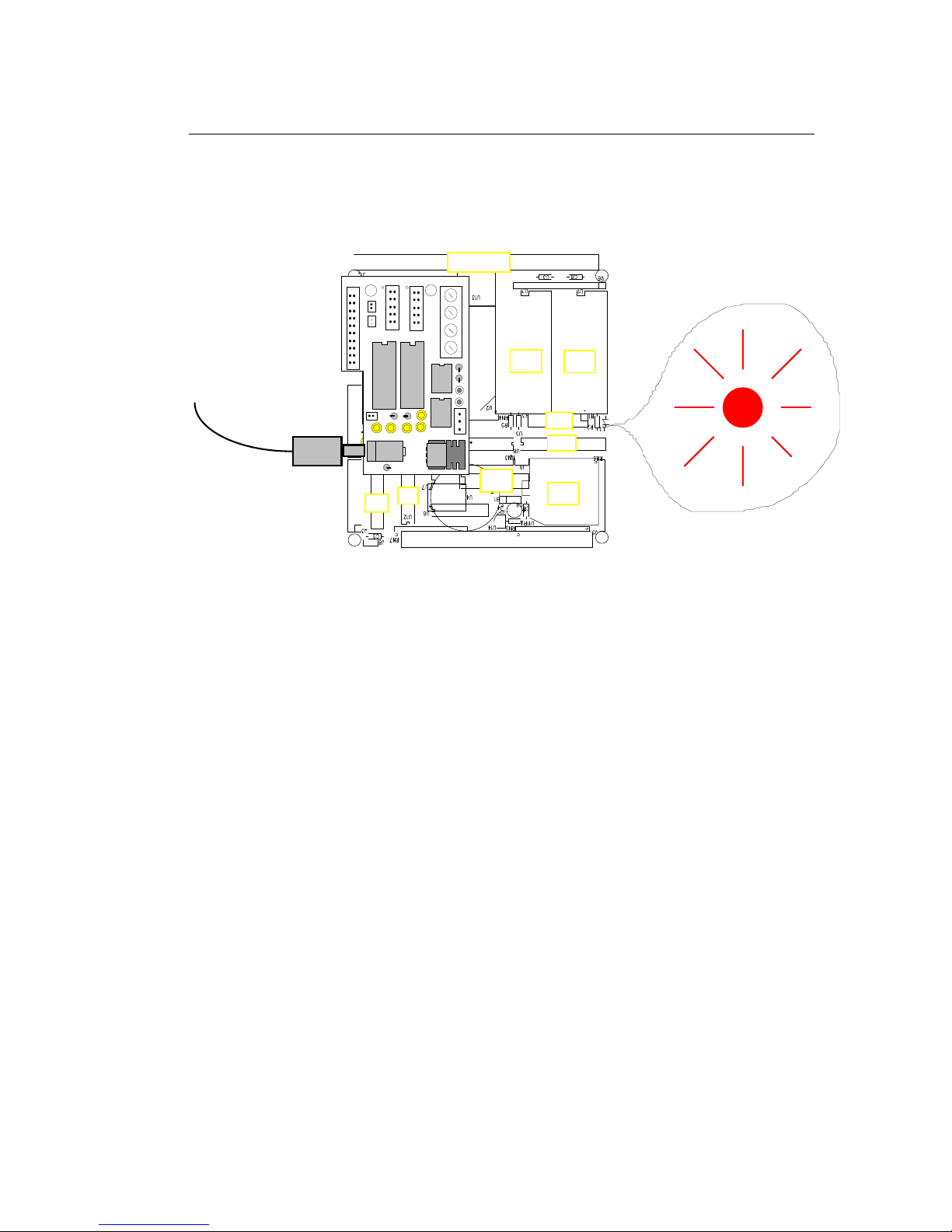
2.2.3 Powering-on the V104
Connect a wall transformer +9V DC output to the VE232 DC power jack.
The on-board LED should blink twice and remain on after the V104 is powered-on or reset (Figure 2.4).
PC/104 Bus
ROM
V25 CPU RAM
LCD
PPI
SCC
AD
DA
RTC
VE232
Figure 2.4 The LED blinks twice after the V104 is powered-on or reset
Page 12

V104 Chapter 3: Hardware
3-1
Chapter 3: Hardware
3.1 V25 I/O Ports
V25 (µPD70320 NEC) is the CPU of the V104. The V25 CPU has 32 I/O lines which are basically
organized as three bi-directional I/O ports(P0-2) and a comparator input port T. The 24 bi-directional I/O
lines are multiplexed with different functions. One I/O line can be specified as an input, output, or a control
line. There are three Special Function Registers (SFR) associated with each port: Port Mode Control
Register (PMC0, PMC1, PMC2), Port Mode Register (PM0, PM1, PM2), and Port Data Register (P0, P1,
P2). The SFRs are memory mapped. You can write or read these registers via
pokeb(0xfff0, 0x??, 0x!!); or peekb(0xfff0, 0x??);
where ?? is the register offset address, !! is the control/data byte.
SFR addresses are listed in the NEC V25 User’s Manual Table 3-2, page 3-8. Port operation tables are
listed in the NEC V25 User’s Manual Figure 7-5, 7-6, and 7-7 in page 7-2 and page 7-3.
For example, in order to use port 0 P05 as output, you need program port 0 in 3 steps:
1) program the PMC0 register and set PMC0 bit 5=0, which defines P05 as I/O function.
2) program PM0 register and set PM0 bit 5=0, which defines P05 as output.
3) Write a “1” to P0 data register bit 5, the P05 pin on the V104 J2-5 should be high (5V).
Write a “0” to P0 data register bit 5, the P05 pin on the V104 J2-5 should be low (0V).
Some I/O lines are used by the V104 system as listed below:
P00 I/O EEPROM (U7 pin 6) clock SCL
P01 I/O EEPROM (U7 pin 5) data SDA
P02 I/O J10 pin 19. If low, jump to application code which
starting address is defined in the on board EEPROM (0x10 to 0x13).
P03* I/O J7 pin 1. HWD (Hit watchdog)
P04* I/O WDO (Read watchdog output, U6 pin 14).
P05* I/O on board LED control
P06 I/O J10 pin 18.
P07 clock out J1 pin 40, CLKOUT, 8 MHz as system clock.
P10 NMI J4 pin 2.
P11* INTP0 J10 pin 17, External Interrupt Input 0, falling edge effective.
V104™ U8 SCC2691 UART interrupt.
P12 INTP1 J1 pin 50, External Interrupt Input 1, falling edge effective.
P13 INTP2 J1 pin 48, External Interrupt Input 2, falling edge effective.
P14* I/O J2 pin 10, may be used as RTS1 for SER1.
P15 I/O J10 pin 16.
P16* I/O J2 pin 14, may be used as RTS0 for SER0.
P17 RDY J10 pin 15, V25 ready signal, used for more wait states, U5.12.
P20 I/O(DR0) J1 pin 36, counter 0/DMA channel 0 request, rising edge active.
P21 I/O(DA0) J1 pin 34, DMA channel 0 Ack, active low, U5.6.
P22 I/O J2 pin 3.
P23 I/O J2 pin 17, counter 1/DMA1/EN485 for SCC RS485 driver.
P24 I/O J10 pin 6 and ADC SCLK.
P25 I/O J10 pin 5 and ADC DIN.
P26 I/O J10 pin 4 and ADC DOUT.
P27 I/O J10 pin 3 and ADC /CS.
PT0 INPUT J10 pin 14.
PT1 INPUT J10 pin 13.
PT2 INPUT J10 pin 12.
PT3 INPUT J10 pin 11.
PT4 INPUT J10 pin 10.
Page 13

Chapter 3: Hardware V104
3-2
PT5 INPUT J10 pin 9.
PT6 INPUT J10 pin 8.
PT7* INPUT J10 pin 7.
P00, P01, P05, P07, P17, P24-27 are used by system and ADC. While using the DEBUG EPROM, P02 is
used to select STEP 1 (DEBUG mode) or STEP 2 (standalone mode) during the power on or reset, see Fig
1.2a for detail. P17 is assigned as RDY signal for inserting more wait states in order to interface with slow
LCD modules. If you do not need LCD functions, you may assign P17 as a I/O function line and cutoff the
pin on the U5 PAL pin 12. I/O lines with * marked are optionally used by system or application. For
example, P05 is used for on board LED control, but P05 is also can be used as for application, if you do not
need LED. P03 can be used to hit watchdog or can be used for your application, if you do not use watchdog.
Due to SFR registers of PMC0-2, PM0-2 are write only, image registers are assigned to locations in the on
board EEPROM at:
PM0 0x08 ee_rd(0x08); or ee_wr(0x08, pm0);
PMC0 0x09 ee_rd(0x09); or ee_wr(0x09, pmc0);
PM1 0x0a ee_rd(0x0a); or ee_wr(0x0a, pm1);
PMC1 0x0b ee_rd(0x0b); or ee_wr(0x0b, pmc1);
PM2 0x0c ee_rd(0x0c); or ee_wr(0x0c, pm2);
PMC2 0x0d ee_rd(0x0d); or ee_wr(0x0d, pmc2);
The ee_rd() and ee_wr() functions are very slow. The EEPROM is only modified by the ve_init();. Other
functions may change the PMCx and PMx registers without modifying the EEPROM. If you need fast
access the image registers, you may use SRAM variables instead.
After ve_init(void);, the initial register control bytes are written into EEPROM. You may use these image
registers to determine the status of the port. You may also need to update these registers in your
applications. The port0-2 are initialized by the ve_init(void) as listed below:
void ve_init(void){
pokeb(0xfff0,0x02,0x80); /* Set PMC0 P07=CLK */
pokeb(0xfff0,0x01,0xd7); /* Set PM0 for input, P05=LED P03=HWD
output */
pokeb(0xfff0,0x0a,0x80); /* Set PMC1 P17 for READY */
pokeb(0xfff0,0x09,0xaf); /* Set PM1 for input, P14=RTS1,P16=RTS0
OUTPUT */
pokeb(0xfff0,0x12,0x00); /* Set P20-P27 for port mode */
pokeb(0xfff0,0x11,0xf7); /* Set PM2 for input, P23=EN485 output */
}
The port data registers can be read and write. In order to modify only one bit, you need to read back the
data byte from that data register first, then do OR/AND operation on that bit.
For example, you can manipulate P05 to low or high with these functions:
pokeb(0xfff0,0x00,(unsigned char) (peekb(0xfff0,0)&0xdf)); /* Set
P05=low */
pokeb(0xfff0,0x00,(unsigned char) (peekb(0xfff0,0)|0x20)); /* Set
P05=high */
3.2 Memory Mapped Devices
All CPU-on-chip peripherals are memory mapped. They are controlled by a bank of 256-byte special
function registers (SFRs). SFRs can be relocated within 1 M-byte V25 memory space. Most of the CPU-onchip peripherals can be reached from J2 and J10.
3.2.1 Interrupts
V25 has a built-in high performance interrupt controller that can control multiple processing of 17 interrupt
sources. Five of these interrupt sources, NMI, INTP0, INTP1, INTP2, and INT are external and accessible
via memory mapped SFRs. The MAX691/LTC691 PFO (Power Failure Output) pin is connected to NMI
Page 14

V104 Chapter 3: Hardware
3-3
via J4 pin 2-3. The user may connect the PFI (Power Failure Input) pin of MAX691 to an external voltage
divider to monitor the power voltage level (Figure 3.1). The PFI pin has been pulled high to VCC with a
10K resistor on the V104. When the external DC power drops and the voltage on the PFI (J2 pin 8) is less
than 1.3 V, the MAX691 will pull down PFO pin, and NMI will occur. You can write a NMI interrupt
service routine to meet your requirements (see Chapter 4, “External Interrupts” for setting an NMI service
routine). V25 CPU has three different methods of responding to an interrupt: vector interrupt functions,
register bank switching functions, and macro service functions. V104 uses vector interrupt. Refer to Chapter
4 and the NEC V25 User's Manual for information about writing interrupt service routines.
External Resistor Divider for Power Failure Detection
47K
2K
PFI of MAX691
(1.3 V min)
(8.35 V min)
9-14 V
10K
VCC = +5V
PT7
Figure 3.1 Using PFI to monitor power voltage level
3.2.2 Comparator Input Port (PORTT)
Port T is an 8-bit comparator input port. The threshold voltage VTH can be fixed to VCC or connected to a
variable voltage source. Software can set the reference voltage to one of 16 levels (1/16xVTH to
16/16xVTH). It provide users with an easy and inexpensive way to measure analog input signals. VTH is
pulled high to VCC via a 10K resistor on board.
3.2.3 External Event Counters / DMA
V25 has two DMA channels, DMA0 and DMA1. The DMA controllers can be used as 16-bit external event
counters. After you set a 16-bit counter value into counter 0 or counter 1 with
counter0_init(unsigned int cnt0); or counter0_init(unsigned int cnt0);
Every rising edge input signal on J1 pin 36 (P20=/DR0) will decrement the counter 0. Every rising edge
input signal on J2 pin 17 (P23) will decrement the counter 1. Be aware of P20 is also used as /LD signal for
the 12-bit DAC. An interrupt will occur, after counting to zero. You need an interrupt service route to serve
the counter interrupt. For more detail, please see a sample program in TERN disk,
a:\samples\ve\ve_count.c.
The V104 supports DMA0 only. There are four different DMA transfer modes, selectable by software. For
memory to memory DMA transfer, the DMAAK0 is not active. For memory to I/O DMA transfer, the
DMAAK0 asserts every DMA cycle. P21 and P20 can be used as I/O pins. For more information refer to
Section 6 of the V25 User's Manual.
3.2.4 Clock and Timers
A built-in clock generator supplies various clocks to the CPU and peripheral hardware. The V104 uses a 16
MHz crystal. Default system clock output after initialization is 8 MHz on CLK line (pin 40 of J1). One
clock cycle is 125 ns. The normal bus cycle requires two clock cycles, which is 250 ns. With built-in wait
state generation, up to 2 wait states can be inserted. Additional wait states can be inserted by using the RDY
line. With the default initialization of 2 wait states, EPROMs of 120 ns to 150 ns can be used. More delays
may be required to support slow I/O devices, such as LCD (Liquid Crystal Display).
The time base counter operates continuously since the V104 is powered on. It provides clock signals for
two 16-bit timers, baud rate generator, refresh timing, refresh address, and time base interrupt request flag.
CLKOUT(P07) and /REFRQ are two outputs of the time base counter. The CLKOUT output to peripheral
hardware. /REFRQ may be used to refresh DRAM in user applications. A time base interrupt is generated at
4 different intervals, 128 us, 1.024 ms, 8.192 ms, and 131.072 ms, selectable by software.
Page 15

Chapter 3: Hardware V104
3-4
Two 16-bit timer units, TM0 and TM1, can operate in interval timer mode or one-shot timer mode. The
TOUT=P15 is available on pin 16 of J10.
3.2.5 Serial Channels
The V104 has three serial channels: two internal UART, SER0, SER1 and one external UART SCC2691
(U8). They can operate in full-duplex communication mode. These serial ports may be used as interruptdriven. For more information about the external UART SCC2691, refer to Appendix C.
The internal serial channels can operate in asynchronous mode and I/O interface mode. In asynchronous
mode, the start/stop bit transmit/receive method is employed so that bit synchronization and character
synchronization are obtained by the start bit. In I/O interface mode, data is transferred in synchronization
with the controlled serial clock. Each internal serial channel includes serial data input RxDn, serial data
output TxDn, and Clear-to-Send signal input (CTSn). Always tie CTS0 and CTS1 to GND, in order to
operate SER0 and SER1. SER0 also has a serial clock output SCKO, which outputs high level in
asynchronous mode, and functions as the transmit clock output pin in interface mode.
For SER0 and SER1, a built-in baud rate generator can be used to select standard baud rates from 110 to
1.25 M. One of these internal serial ports is used by the V104 for programming with the PC. It uses 115,000
Baud rate for programming. It is possible to use both SER0 and SER1 in applications. The user can use
SER0 to debug an application program for SER1, and then use SER1 to debug application programs for
SER0. The application programs can be combined and downloaded via either serial channel. Application
program using both SER0 and SER1 can run at the same time, but not debug at the same time.
3.2.6 Halt and Stop Mode
The V104 is an ideal core module for low power consumption applications, such as a battery operated
instrument. V25 has two standby modes, which are set by halt(); and stop(); In the HALT mode, the CPU
clock is stopped and program execution is halted, the registers are retained, and peripheral hardware
continues to function. The total power consumption is approximately 10 mA. The HALT mode is released
by interrupt input or reset input. In STOP mode, all clocks stop, but data in registers and RAM are retained.
The total power consumption is less than 4 mA. The STOP mode only can be released by NMI input or
reset input.
3.3 I/O Space Mapped Devices
External I/O device use I/O mapping. You may access I/O with inportb(port) or outportb(port,dat);. The
external I/O space is 64K, ranging from 0x0000 to 0xffff. In the I/O space of 0x0000-0x7fff, the I/O access
time is 500 ns. In the I/O space of 0x8000-0xffff, the I/O access time is 250 ns. Table 5.3 shows more
information of I/O mapped devices:
I/O space time(ns) Decodes Usage
---------------------------------------------------------------------------------------------------------------------0x0010-0x3fff >500 ns USER
0x4000-0x40ff >500 ns lcd3
0x4100-0x41ff >500 ns lcd4
0x8000-0xbfff >250 ns RTC
0xc000-0xc0ff >250 ns E=SCC
0xc100-0xc1ff >250 ns PPI
Table 3.1 Information for interface with I/O space mapped devices
3.3.2 Programmable Peripheral Interface (82C55A)
U11 PPI (82C55) is a low-power CMOS programmable parallel interface unit for use in microcomputer
systems. It provides 24 I/O pins that may be individually programmed in two groups of 12 and used in
three major modes of operation.
Page 16
V104 Chapter 3: Hardware
3-5
In MODE 0, the two groups of 12 pins can be programmed in sets of 4 and 8 pins to be inputs or outputs.
In MODE 1, each of the two groups of 12 pins can be programmed to have 8 lines of input or output. Of
the 4 remaining pins, 3 are used for handshaking and interrupt control signals. MODE 2 is a strobed bi-
directional bus configuration.
7601234
5
G R O U P 1
P o r t 2
(L o w e r )
P o r t 1
M o d e
0
1
0
1
0
1
O u tp u t
In p u t
O u tp u t
In p u t
M o d e 0
M o d e 1
G R O U P 2
P o r t 2
(U p p er)
P o r t 0
M o d e
0
1
0
1
0 0
0 1
O u tp u t
In p u t
O u tp u t
In p u t
M o d e 0
M o d e 1
M o d e 2
1 X
C o m m a n d
S el e c t
0
1
B it
m a n i p u la t io n
M o d e
S ele ct
Figure 3.2 Mode Select Command Word
The V104 maps U11, the 82C55/uPD71055, in I/O space to 0xC100 to 0xC103.
The Command Register = 0xC103.
Port 0 = 0xC100.
Port 1 = 0xC101.
Port 2 = 0xC102.
The following code example will set all ports to output mode:
outportb(0xC103,0x80); /* Mode 0 all output selection. */
outportb(0xC100,0x55); /* Sets port 0 to alternating high/low I/O
pins. */
outportb(0xC101,0x55); /* Sets port 1 to alternating high/low I/O
pins. */
outportb(0xC102,0x55); /* Sets port 2 to alternating high/low I/O
pins. */
To set all ports to input mode:
outportb(0xC103,0x9f); /* Mode 0 all input selection. */
You may read the ports with:
inportb(0xC100); /* Port 0 */
inportb(0xC101); /* Port 1 */
inportb(0xC102); /* Port 2 */
Page 17

Chapter 3: Hardware V104
3-6
This returns an 8-bit value for each port, with each bit corresponding to the appropriate line on the port.
You will find that numerous on-board components are controlled using PPI lines only. You will need to use
PPI access methods to control these, as well.
The V104 J5 header pin layout is as follows:
Pin 1 = I10 Pin 2 = GND
Pin 3 = I11 Pin 4 = GND
Pin 5 = I12 Pin 6 = GND
Pin 7 = I13 Pin 8 = GND
Pin 9 = I14 Pin 10 = GND
Pin 11 = I15 Pin 12 = GND
Pin 13 = I16 Pin 14 = GND
Pin 15 = I17 Pin 16 = GND
Pin 17 = I20 Pin 18 = GND
Pin 19 = I21 Pin 20 = GND
Pin 21 = I22 Pin 22 = GND
Pin 23 = I23 Pin 24 = GND
Pin 25 = I24 Pin 26 = GND
Pin 27 = I25 Pin 28 = GND
Pin 29 = I26 Pin 30 = GND
Pin 31 = I27 Pin 32 = GND
Pin 33 = I00 Pin 34 = GND
Pin 35 = I01 Pin 36 = GND
Pin 37 = I02 Pin 38 = GND
Pin 39 = I03 Pin 40 = GND
Pin 41 = I04 Pin 42 = GND
Pin 43 = I05 Pin 44 = GND
Pin 45 = I06 Pin 46 = GND
Pin 47 = I07 Pin 48 = GND
Pin 49 = VCC Pin 50 = GND
For more information on this device, please refer to the NEC uPD71055 datasheet (415-960-6000).
3.3.3 RTC72421
A real-time clock RTC72421 (EPSON, U4) is mapped in the I/O address space 0x8000-0xbffff. It must be
backed up with a lithium coin battery. The RTC may be accessed via software drivers rtc_init() or rtc_rd();
(see Chapter 4). Details are listed in Appendix D.
3.3.4 UART SCC2691
The UART SCC2691 (Signetics, U8) is mapped in the I/O address space 0xc000-0xc0ff. The SCC2691 has
a full-duplex asynchronous receiver/transmitter, a quadruple buffered receiver data register, an interrupt
control mechanism, programmable data format, selectable Baud rate for the receiver and transmitter, a
multi-functional and programmable 16-bit counter/timer, an on-chip crystal oscillator, and a multi-purpose
input/output including RTS and CTS mechanism. For more information, refer to Appendix C. The
SCC2691 on the V104 may be used as a network 9th-bit UART. The RxD and TxD signals are routed to the
J2 header for connecting to a VE232. Use J1 pin 3 (RS485-) and pin 4 (RS485+) on the VE232 to join the
multi-drop RS485 twist pair network. The MPO and MPI are routed to J9 of the V104.
3.4 Other Devices
3.4.1 MAX691
The MAX691/LTC691 (U6) is a supervisor chip. With it installed, the V104 has several functions that
significantly improve system reliability:
Page 18

V104 Chapter 3: Hardware
3-7
• watchdog timer
• power-failure warning
• battery backup
• power-on-reset delay
• power-supply monitoring
The V104 uses P03 to hit the watchdog timer via J7 1-2.
Watchdog Timer
The watchdog timer is activated by setting a jumper on J7 pins 1-2 of the V104. The watchdog timer
provides a means of verifying proper software execution. In the user's application program, calls to the
function hitwd() (a routine that toggles the P03=HWD pin of the MAX691) should be arranged such that
the HWD pin is accessed at least once every 1.6 seconds. If the J7 1-2 jumper is on and the HWD pin is not
accessed within this time-out period, the watchdog timer pulls the WDO pin low, which asserts /RESET.
This automatic assertion of /RESET may recover the application program if something is wrong. After the
V104 is reset, WDO remains low until a transition occurs at the WDI pin of the MAX691. When controllers
are shipped from the factory the J7 jumper is off, which disables the watchdog timer.
Power-failure Warning and Battery Backup
If a jumper is put on the J4 1-2, then the NMI is connected to the PFO (Power Failure Output) pin of the
MAX691. When the power failure is sensed by the PFI pin of the MAX691 (lower than 1.3 V, Figure 3.1),
the PFO pulls NMI low, and an NMI interrupt occurs before the power-failure occurs. You may design a
NMI service routine to take protect actions before the +5V drops and processor dies. The battery-switch-
over circuit compares VCC to VBAT (+3 V lithium battery positive pin), and connects whichever is higher
to the VRAM (power for SRAM and RTC). Thus, the SRAM and the real-time clock RTC72421 are
backed up. The lithium battery will last about 5-10 years in normal use. When the external power is on, the
battery-switch-over circuit will select the VCC to connect to the VRAM.
J1 = PC/104 Bus
ROM
V25 CPU RAM
LCD
PPI
SCC
AD
DA
RTC
0, 0
3.5x4.0
J6
Memory Select
ROM 32-64K 1-2
ROM >64K 2-3
RAM 32-128K 5-6
RAM > 128K 4-5
EPROM 8-9
Flash 7-8
ROM 512K 10-11
J9
=SCC MPO MPI
J4
VOFF NMI PFO
J5 24 I/O lines
J7
Enable WD 1-2
Enable EE R/W 4-5
J3 ADC, DAC
J10 V25 I/O lines
J2 VE232 interface
J8 RESET
LED
STEP 2 Jumper
P02 and GND
Figure 3.3 Jumper settings on the V104
Page 19

Chapter 3: Hardware V104
3-8
3.4.2 EEPROM
A serial EEPROM of 128 bytes (24C01), 512 bytes (24C04), or 2K bytes (24C16) can be installed in U7.
The V25-Engine uses the P00=SCL (serial clock) and P01=SDA (serial data) to interface with the
EEPROM. The EEPROM can be used to store important data such as a node address, calibration
coefficients, and configuration codes. It typically has 1,000,000 erase/write cycles, and the data retention is
more than 40 years. EEPROM can be read and written to by simply calling the functions ee_rd() and
ee_wr().
3.4.3 12-bit ADC (TLC2543)
The TLC2543 is a 12-bit, switched-capacitor, successive-approximation, 11 channels, serial interface,
analog-to-digital converter. It has three control inputs (/CS=P27; CLK=P24; DIN=P25) and is designed for
communication with a host through a serial tri-state output(DOUT=P26). If P27 is low, the TLC2543 will
have output on P26. If P27 is high, the TLC2543 is disabled and P24, P25, P26 are free. P27 is pulled high
by a 10K resistor on board. The TLC2543 has an on-chip 14 channel multiplexer that can select any one of
11 inputs or any one of three internal self-test voltages. The sample-and-hold function is automatic. At the
end of conversion, the end-of-conversion output goes high to indicate that conversion is complete.
TLC2543 features differential high-impedance inputs that facilitate ratiometric conversion, scaling, and
isolation of analog circuitry from logic and supply noise. A switched-capacitor design allows low-error
conversion over the full operating temperature range. The analog input signal source impedance should be
less than 50Ω and capable of slewing the analog input voltage into a 60 pF capacitor.
You may read the ADC with the function in the library: ce_ad12(ch);
In order to operate the TLC2543, five V25 I/O lines are used as listed below:
/CS Chip select = P27, high to low transition enables DOUT, DIN and CLK.
low to high transition disables DOUT, DIN and CLK.
DIN P25, serial data input
DOUT P26, 3-state serial data output.
CLK I/O clock = P24
REF+ Upper reference voltage(normally VCC)
REF- Lower reference voltage(normally GND)
VCC Power supply, +5 V input
GND Ground
The analog inputs AD0 to AD10, REF+, GND, and VCC are available at J3 connector.
3.4.4 12-bit DAC (MAX537)
The MAX537 combines four 12-bit, voltage output digital to analog converters and four precision output
amplifiers in a 16 pin chip. The MAX537 operates with ±5V power supply. Each DAC has a doublebuffered input. A 16-bit serial word is used to load data into input/DAC register. The V104 uses P20=/LD,
P21=DAC /CS, P24=SCLK, and P25=SDI to operate the MAX537. The REF+ of the MAX537 is 2.5V
provided by U14. You may write the DAC with the function in the library: v104_da12(ch, dat);
3.5 Jumpers and Headers
There are 14 jumpers and connectors on the V104.
Name Size Function
J1 32x2 PC/104 compatible bus
J2 10x2 VE232 interface
J3 10x2 Analog inputs, analog outputs and reference
J4 3x1 VOFF, /NMI and /PFO
J5 25x2 24 bi-directional I/O pins, +5V and GND
J6 12x1 Memory selection, see Figure 3.3
Page 20

V104 Chapter 3: Hardware
3-9
J7 5x1 pin 1=2 Enable watchdog timer.
pin 3=4, Enable EEPROM write protection, pin 4=5 no write protection
J8 2x1 Reset.
J9 2x1 SCC2691 MPO and MPI
H1 8x2 LCD interface
H2 2x1 UART SCC2691 MPO and MPI
Page 21

V104 Chapter 4: Software
4-1
Chapter 4: Software
Please refer to the Technical Manual of the “C/C++ Development Kit for TERN 16-bit Embedded
Microcontrollers” for details on debugging and programming tools.
For details regarding software function prototypes and sample files demonstrating their use, please refer to
the Software Glossary in Appendix F.
Guidelines, awareness, and problems in an interrupt driven environment
Although the C/C++ Development Kit provides a simple, low cost solution to application engineers, some
guidelines must be followed. If they are not followed, you may experience system crashes, PC hang-ups,
and other problems.
The debugging of interrupt handlers with the Remote Debugger can be a challenge. It is possible to debug
an interrupt handler, but there is a risk of experiencing problems. Most problems occur in multi-interruptdriven situations. Because the remote kernel running on the controller is interrupt-driven, it demands
interrupt services from the CPU. If an application program enables interrupt and occupies the interrupt
controller for longer than the remote debugger can accept, the debugger will time-out. As a result, your PC
may hang-up. In extreme cases, a power reset may be required to restart your PC.
For your reference, be aware that our system is remote kernel interrupt-driven for debugging.
The run-time environment on TERN controllers consists of an I/O address space and a memory address
space. I/O address space ranges from 0x0000 to 0xffff, or 64 KB. Memory address space ranges from
0x00000 to 0xfffff in real-mode, or 1 MB. These are accessed differently, and not all addresses can be
translated and handled correctly by hardware. I/O and memory mappings are done in software to define
how translations are implemented by the hardware. Implicit accesses to I/O and memory address space
occur throughout your program from TERN libraries as well as simple memory accesses to either code or
global and stack data. You can, however, explicitly access any address in I/O or memory space, and you
will probably need to do so in order to access processor registers and on-board peripheral components
(which often reside in I/O space) or non-mapped memory.
This is done with four different sets of similar functions, described below.
poke/pokeb
Arguments: unsigned int segment, unsigned int offset, unsigned int/unsigned char data
Return value: none
These standard C functions are used to place specified data at any memory space location. The segment
argument is left shifted by four and added to the offset argument to indicate the 20-bit address within
memory space. poke is used for writing 16 bits at a time, and pokeb is used for writing 8 bits.
The process of placing data into memory space means that the appropriate address and data are placed on
the address and data-bus, and any memory-space mappings in place for this particular range of memory will
be used to activate appropriate chip-select lines and the corresponding hardware component responsible for
handling this data.
Page 22

4-2
peek/peekb
Arguments: unsigned int segment, unsigned int offset
Return value: unsigned int/unsigned char data
These functions retrieve the data for a specified address in memory space. Once again, the segment address
is shifted left by four bits and added to the offset to find the 20-bit address. This address is then output over
the address bus, and the hardware component mapped to that address should return either an 8-bit value or a
16-bit value over the data bus. If there is no component mapped to that address, this function will return
random garbage values every time you try to peek into that address.
outport/outportb
Arguments: unsigned int address, unsigned int/unsigned char data
Return value: none
This function is used to place the data into the appropriate address in I/O space. It is used most often when
working with processor registers that are mapped into I/O space and must be accessed using either one of
these functions. This is also the function used in most cases when dealing with user-configured peripheral
components.
When dealing with processor registers, be sure to use the correct function. Use outport if you are dealing
with a 16-bit register.
inport/inportb
Arguments: unsigned int address
Return value: unsigned int/unsigned char data
This function can be used to retrieve data from components in I/O space. You will find that most hardware
options added to TERN controllers are mapped into I/O space, since memory space is valuable and is
reserved for uses related to the code and data. Using I/O mappings, the address is output over the address
bus, and the returned 16 or 8-bit value is the return value.
For a further discussion of I/O and memory mappings, please refer to the Hardware chapter of this technical
manual.
4.1 VE.LIB
VE.LIB is a C library for basic V104 operations. It includes the following modules: VE.OBJ, SER0.OBJ,
SER1.OBJ, SCC.OBJ, VEEE.OBJ. You need to link VE.LIB in your applications and include the
corresponding header files. The following is a list of the header files:
Include-file name Description
VE.H PPI, timer/counter, ADC, DAC, RTC, Watchdog,
SER0.H Internal serial port 0
SER1.H Internal serial port 1
SCC.H External UART SCC2691
VEEE.H on-board EEPROM
Page 23

4-3
4.2 Functions in VE.OBJ
4.2.1 V104 Initialization
VE_init
This function should be called at the beginning of every program running on V104 core controllers. It
provides default initialization and configuration of the various I/O pins, interrupt vectors, sets up expanded
DOS I/O, and provides other processor-specific updates needed at the beginning of every program.
ve_init will initialize the I/O pin functions and store the initial register control bytes into the EEPROM (see
Appendix E). You may use these image registers to determine the status of the port but you must update
these registers in your applications. The port0-2 are initialized as shown below:
void ve_init(void){
pokeb(0xfff0,0x02,0x80); /* Set PMC0 P07=CLK */
pokeb(0xfff0,0x01,0xd7); /* Set PM0 for input, P05=LED P03=HWD output */
pokeb(0xfff0,0x0a,0x80); /* Set PMC1 P17 for READY */
pokeb(0xfff0,0x09,0xaf); /* Set PM1 for input, P14=RTS1,P16=RTS0 OUTPUT */
pokeb(0xfff0,0x12,0x00); /* Set P20-P27 for port mode */
4.2.2 External Interrupt Initialization
There are up to five external interrupt sources on the V104, consisting of four maskable interrupt pins
(INTP2-INTP0, INT) and one non-maskable interrupt (NMI). There are also additional internal interrupt
sources not connected to the external pins, consisting of two timers, a time base counter, two DMA
channels, both asynchronous serial ports, and the NMI from the watchdog timer. For a detailed discussion
involving the interrupts, the user should refer to chapter 4 of the NEC V25 CPU User’s Manual.
TERN provides functions to enable/disable all of the external interrupts. The user can call any of the
interrupt init functions listed below for this purpose. The first argument indicates whether the particular
interrupt should be enabled, and the second is a function pointer to an appropriate interrupt service routine
that should be used to handle the interrupt. The TERN libraries will set up the interrupt vectors correctly
for the specified external interrupt line.
At the end of interrupt handlers, the user should run a finish interrupt routine. This can be done using the
fint() function.
void intpx_init
Arguments: unsigned char i, void interrupt far(* intpx_isr) () )
Return value: none
These functions can be used to initialize any one of the external interrupt channels (for pin locations and
other physical hardware details, see the Hardware chapter). The first argument i indicates whether this
particular interrupt should be enabled or disabled. The second argument is a function pointer that will act
as the interrupt service routine.
By default, the interrupts are all disabled after initialization. To disable them again, you can repeat the call
but pass in 0 as the first argument.
The NMI (Non-Maskable Interrupt) is special in that it can not be masked (disabled). The default ISR will
return on interrupt.
void nmi_init(void);
void intp0_init( unsigned char i, void interrupt far(* int0_isr)() );
void intp1_init( unsigned char i, void interrupt far(* int1_isr)() );
void intp2_init( unsigned char i, void interrupt far(* int2_isr)() );
Page 24

4-4
void timer0_init(unsigned char i, void interrupt far(* timer0_isr)());
void timer1_init(unsigned char i, void interrupt far(* timer1_isr)());
void timer2_init(unsigned char i, void interrupt far(* timer2_isr)());
void time_base_init(char i, void interrupt far(*time_base_isr)());
4.2.3 I/O Initialization
There are two ports of 16 I/O pins available on the V104. Hardware details regarding these PIO lines can be
found in the Hardware chapter.
There are several functions provided for access to the PIO lines. At the beginning of any application where
you choose to use the PIO pins as input/output, you will probably need to initialize these pins in one of the
four available modes. Before selecting pins for this purpose, make sure that the peripheral mode operation
of the pin is not needed for a different use within the same application.
You should also confirm the PIO usage that is described above within ve_init(). During initialization,
several lines are reserved for TERN usage and you should understand that these are not available for your
application. There are several PIO lines that are used for other on-board purposes. These are all described
in some detail in the Hardware chapter of this technical manual. For a detailed discussion of the I/O ports,
please refer to chapter 7 of the NEC V25 User’s Manual.
Please see the sample program portx.c in tern\v25\samples\ve. You will also find that these
functions are used throughout TERN sample files, as most applications do find it necessary to re-configure
the PIO lines.
The functions port_wr and port_rd can be quite slow when accessing the Port I/O pins. The maximum
efficiency you can get from the Port I/O pins occurs if you modify the Port registers directly with an
outport instruction instead of using port_wr/port_rd.
See the Hardware chapter for Port register addresses.
void port_init
Arguments: char p, unsigned char pmc, unsigned char pm
Return value: none
p refers to Port 0, Port 1 or Port2.
pmc refers to the 8-bit port mode control register value for port p.
• A ‘0’ bit sets the pin to I/O mode
• A ‘1’ bit sets the pin to CONTROL mode
pm refers to the 8-bit port mode register value for port p. This register is valid for pins only I/O mode pins.
• A ‘0’ bit sets the pin to output
• A ‘1’ bit sets the pin to input
char port_rd
Arguments: char p
Return value: byte indicating Port I/O status for port p.
Each bit of the returned 8-bit value indicates the current I/O value for the Port I/O pins in port p.
void pio_wr
Arguments: char p, char dat
Return value: none
Writes an 8-bit value to port p. Only changes status of I/O mode output pins.
Page 25

4-5
Example 4.1
Set port 0 as I/O, bits 0 – 3 as input, 4 – 7 as output.
port_init(0, 0x00, 0xf0);
p = Port 0,
pmc = 0 (I/O),
pm 0-3 = 1, pm 4-7 = 0.
Example 4.2
Set pins 20 and 23 as DMA Request. All other port 2 pins as output.
port_init(2, 0x09, 0x00);
p = Port 2,
pmc = bit 0 and 3 = 1 (Control), all others = 0 (I/O)
pm = all 0s. Since pins 20 and 23 are control functions, the pm field is not
relevant.
In most cases it is only necessary to change the value of one or two pins in the port data register Since the
port data register is a read/write register, it is possible to mask the pins that do not need to change. In this
case, the port_init function cannot be used. Instead, the port data register can be directly accessed using the
poke and peek functions.
Example 4.3
Using bitwise OR to set a single bit high, set pin 23 high without
modifying the other pins. Assume all port 2 is output and that all pins
are low.
pokeb(0xfff0, 0x10, (unsigned char) (peekb( 0xfff0, 0x10) | 0x08) );
Assuming that all of port 2 is outputting low, the peekb function will return a value of
0x00. A bitwise ‘OR’ with the value 0x00 and the mask 0x08 equals 0x08.
Port 2 now outputs 0x08.
Example 4.4
Using bitwise AND to reset a single bit low, set pin 23 low without
modifying the other pins. Assume settings are the same after executing
Example 4.3.
pokeb(0xfff0, 0x10, (unsigned char) (peekb( 0xfff0, 0x10) & 0xF7 ) );
Assuming the settings from Example 4.3 are still present, the peekb function should return
a value of 0x08. A bitwise ‘AND’ with the value 0x08 and the mask 0xF7
equals 0x00. Port is again set to 0x00 (all pins low).
While the port data registers are read/write registers, the port control registers pmc and pm are not.
Modifying only certain pins in these registers requires the use of global variables to store the values of these
registers. This means that any changes to the pmc or pm registers must be accounted for in the global
variable. As in the previous example, the bitwise OR and AND expressions can be used to mask the
register bits.
Example 4.5
Set port 2 pins 0 through 3 as output.
// The following global variable defines the pm2 register
unsigned char pm2;
Page 26

4-6
/* assume pm2 has been correctly maintained. The following code will modify the pm2
register such that bits 0 through 3 are low. Use AND to set bits low */
pokeb(0xfff0, 0x11, ( pm2 = ( pm2 & 0xF0 ) ) ); //pm2 must be set to a new register
value
Example 4.6
Set port 2 pins 0 through 3 as input.
// The following global variable defines the pm2 register
unsigned char pm2;
/* assume pm2 has been correctly maintained. The following code will modify the pm2
register such that bits 0 through 3 are high. Use OR to set bits high */
pokeb(0xfff0, 0x11, ( pm2 = ( pm2 | 0x0F ) ) ); //pm2 must be set to new register value
4.2.4 Port T
Port T is an 8-bit input port whose threshold voltage can be changed in 16 steps. Comparator operation is
performed through this port. Each Port T input is compared with the selected threshold voltage (Vth). PTn
> Vth results in a value 1, PTn < Vth results in a value 0. All eight results from PT0 to PT7 are latched to
the port T input latches.
The resulting 8-bit latch can be accessed by the function portt_rd(void) which returns the 8-bit result. Vth
can be changed by the function portt_wr(char vref). The variable vref {0 .. 15} sets the reference voltage
by the following equation: Reference = Vth * vref/16. vref = 0 sets Reference = Vth. Vth is connected to
a 10 K pullup resistor network and Vth ≈ 3.57V. PT0 – PT6 are on J2. PT0 – PT2 are pulled up by 10k
resistors.
void portt_wr(char vref)
where vref is a number to select VREF
vref = 0 VTHx 1
vref = 1 VTHx 1/16
vref = 2 VTHx 2/16
vref = 3 VTHx 3/16
vref = 4 VTHx 4/16
vref = 5 VTHx 5/16
vref = 6 VTHx 6/16
vref = 7 VTHx 7/16
vref = 8 VTHx 8/16
vref = 9 VTHx 9/16
vref = 10 VTHx 10/16
vref = 11 VTHx 11/16
vref = 12 VTHx 12/16
vref = 13 VTHx 13/16
vref = 14 VTHx 14/16
vref = 15 VTHx 15/16
char portt_rd(void)
returns an 8-bit character representing the comparator output if the voltage at PT0 < Vref, bit 0=0 else 1.
Page 27

4-7
4.2.5 Timer Units
The two timers present on the V104 can be used for a variety of applications. The timers run at a maximum
of 1/6 of the processor clock rate, which determines the maximum resolution that can be obtained.
These timers are controlled and configured through a mode register that is specified using the software
interfaces. The mode register is described in detail in chapter 9 of the NEC V25 User’s Manual.
The timers can be used to time execution of your user-defined code by reading the timer values before and
after execution of any piece of code. For a sample file demonstrating this application, see the sample file
timer.c in the directory tern\v25\samples\ve.
The specific behavior that you might want to implement is described in detail in chapter 9 of the NEC V25
User’s Manual.
void timer0_init
void timer1_init
Arguments: unsigned char mode, unsigned int md0, unsigned int tm0
Return values: none
The argument mode is the value that you wish placed into the TMC0/TMC1 mode registers for configuring
the two timers.
The argument md0 is the modulo timer count and t0 is the timer count.
void timer0_interrupt
void timer1_interrupt
Arguments: unsigned char i, void interrupt far (* timer0_isr)()
Return values: none
The argument i enables the interrupt and (*timer0_isr)() or (*timer1_isr)() points to the interrupt service
routine. The interrupt service routine is called whenever count 0 is reached, with other behavior possible
depending on the value specified for the control register.
4.2.6 Other library functions
On-board supervisor MAX691 or LTC691
The watchdog timer offered by the MAX691 or LTC691 offers an excellent way to monitor improper
program execution. If the watchdog timer (J9) jumper is set, the function hitwd() must be called every 1.6
seconds of program execution. If this is not executed because of a run-time error, such as an infinite loop or
stalled interrupt service routine, a hardware reset will occur.
void hitwd
Arguments: none
Return value: none
Resets the supervisor timer for another 1.6 seconds.
void led
Arguments: int ledd
Return value: none
Turns the on-board LED on or off according to the value of ledd.
Page 28

4-8
Real-Time Clock
The real-time clock can be used to keep track of real time. Backed up by a lithium-coin battery, the real
time clock can be accessed and programmed using two interface functions.
The real time clock only allows storage of two digits of the year code, as reflected below. As a result,
application developers should be careful to account for a roll-over in digits in the year 2000. One solution
might be to store an offset value in non-volatile storage such as the EEPROM.
A common data structure is used to access and use both interfaces.
typedef struct{
unsigned char sec1; One second digit.
unsigned char sec10; Ten second digit.
unsigned char min1; One minute digit.
unsigned char min10; Ten minute digit.
unsigned char hour1; One hour digit.
unsigned char hour10; Ten hour digit.
unsigned char day1; One day digit.
unsigned char day10; Ten day digit.
unsigned char mon1; One month digit.
unsigned char mon10; Ten month digit.
unsigned char year1; One year digit.
unsigned char year10; Ten year digit.
unsigned char wk; Day of the week.
} TIM;
int rtc_rd
Arguments: TIM *r
Return value: int error_code
This function places the current value of the real time clock within the argument r structure. The structure
should be allocated by the user. This function returns 0 on success and returns 1 in case of error, such as
the clock failing to respond.
Void rtc_init
Arguments: char* t
Return value: none
This function is used to initialize and set a value into the real-time clock. The argument t should be a nullterminated byte array that contains the new time value to be used.
The byte array should correspond to { weekday, year10, year1, month10, month1, day10, day1, hour10,
hour1, minute10, minute1, second10, second1, 0 }.
If, for example, the time to be initialized into the real time clock is June 5, 1998, Friday, 13:55:30, the byte
array would be initialized to:
unsigned char t[14] = { 5, 9, 8, 0, 6, 0, 5, 1, 3, 5, 5, 3, 0 };
Delay
In many applications it becomes useful to pause before executing any further code. There are functions
provided to make this process easy. For applications that require precision timing, you should use the
hardware timers provided on-board for this purpose.
void delay0
Arguments: unsigned int t
Page 29

4-9
Return value: none
This function is just a simple software loop. The actual time that it waits depends on processor speed as
well as interrupt latency. The code is functionally identical to:
While(t) { t--; }
Passing in a t value of 600 causes a delay of approximately 1 ms.
void delay_ms
Arguments: unsigned int
Return value: none
This function is similar to delay0, but the passed in argument is in units of milliseconds instead of loop
iterations. Again, this function is highly dependent upon the processor speed.
unsigned int crc16
Arguments: unsigned char *wptr, unsigned int count
Return value: unsigned int value
This function returns a simple 16-bit CRC on a byte-array of count size pointed to by wptr.
void ve_reset
Arguments: none
Return value: none
This function is similar to a hardware reset, and can be used if your program needs to re-start the board for
any reason. Depending on the current hardware configuration, this might either start executing code from
the DEBUG ROM or from some other address.
4.3 Functions in SER0.OBJ/SER1.OBJ
The functions described in this section are prototyped in the header files ser0.h and ser1.h in the
tern\v25\include directory.
The internal asynchronous serial ports are functionally identical. SER0 is used by the DEBUG ROM
provided as part of the TERN EV/DV software kits for communication with the PC. As a result, you will
not be able to debug code directly written for serial port 0.
Two asynchronous serial ports are integrated in the NEC V25 CPU: SER0 and SER1. Both ports have
baud rates based on the 8 MHz clock.
By default, SER0 is used by the DEBUG ROM for application download/debugging in Step One and Step
Two. We will use SER1 as the example in the following discussion; any of the interface functions that are
specific to SER1 can be easily changed into function calls for SER0. While selecting a serial port for use,
please realize that some pins might be shared with other peripheral functions. This means that in certain
limited cases, it might not be possible to use a certain serial port with other on-board controller functions.
For details, you should see chapter 11 of the NEC V25 User’s Manual.
TERN interface functions make it possible to use one of a number of predetermined baud rates. These baud
rates are achieved by specifying a divisor for the processor frequency.
The following table shows the function arguments that express each baud rate, to be used in TERN
functions.
Function Argument Baud Rate
Page 30

4-10
Function Argument Baud Rate
1 110
2 150
3 300
4 600
5 1200
6 2400
7 4800
8 9600
9 19,200 (default)
10 38,400
11 57,600
12 76,800
13 115,000
14 230,000
15 460,800
16 1 Meg
Table 4.1 Baud rate values
After initialization by calling s1_init(), SER1 is configured as a full-duplex serial port and is ready to
transmit/receive serial data at one of the specified 16 baud rates.
An input buffer, ser1_in_buf (whose size is specified by the user), will automatically store the receiving
serial data stream into the memory by macro service operation. In terms of receiving, there is no software
overhead or interrupt latency for user application programs even at the highest baud rate. Macro service
transfer allows efficient handling of incoming data. The user only has to check the buffer status with
serhit1() and take out the data from the buffer with getser1(), if any. The input buffer is used as a
circular ring buffer, as shown in Figure 4.1. However, the transmit operation is interrupt-driven.
ibuf in_tail ibuf+isizin_head
Figure 4.1 Circular ring input buffer
The input buffer (ibuf), buffer size (isiz), mode (mode), and baud rate (baud) are specified by the user with
s1_init().The mode is the setting value for the serial port control register. A value of 0xC9 will set the
serial port in the following manner:
transmit enable, receive enable, no parity, 8 data bits, 1 stop bit
Due to the nature of high-speed baud rates and possible effects from the external environment, serial input
data will automatically fill in the buffer circularly without stopping, regardless of overwrite. If the user does
not take out the data from the ring buffer with getser1() before the ring buffer is full, new data will
overwrite the old data without warning or control. Thus it is important to provide a sufficiently large buffer
if large amounts of data are transferred. For example, if you are receiving data at 9600 baud, a 4 KB buffer
will be able to store data for approximately four seconds.
Page 31

4-11
However, it is always important to take out data early from the input buffer, before the ring buffer rolls
over. You may designate a higher baud rate for transmitting data out and a slower baud rate for receiving
data. This will give you more time to do other things, without overrunning the input buffer. You can use
serhit1() to check the status of the input buffer and return the offset of the in_head pointer from the
in_tail pointer. A return value of 0 indicates no data is available in the buffer.
You can use getser1() to get the serial input data byte by byte using FIFO from the buffer. The in_tail
pointer will automatically increment after every getser1() call. It is not necessary to suspend external
devices from sending in serial data with /RTS. Only a hardware reset or s1_close() can stop this
receiving operation.
For transmission, you can use putser1() to send out a byte, or use putsers1() to transmit a
character string. You can put data into the transmit ring buffer, s1_out_buf, at any time using this
method. The transmit ring buffer address (obuf) and buffer length (osiz) are also specified at the time of
initialization. The transmit interrupt service will check the availability of data in the transmit buffer. If there
is no more data (the head and tail pointers are equal), it will disable the transmit interrupt. Otherwise, it will
continue to take out the data from the out buffer, and transmit. After you call putser1() and transmit
functions, you are free to do other tasks with no additional software overhead on the transmitting operation.
It will automatically send out all the data you specify. After all data has been sent, it will clear the busy flag
and be ready for the next transmission.
The sample program ser1_0.c demonstrates how a protocol translator works. It would receive an input
HEX file from SER1 and translate every ‘:’ character to ‘?’. The translated HEX file is then transmitted out
of SER0. This sample program can be found in tern\186\samples\ve.
Software Interface
Before you can use the serial ports, they must be initialized.
There is a data structure containing important serial port state information that is passed as argument to the
TERN library interface functions. The COM structure should normally be manipulated only by TERN
libraries. It is provided to make debugging of the serial communication ports more practical. Since it
allows you to monitor the current value of the buffer and associated pointer values, you can watch the
transmission process.
The two serial ports have similar software interfaces. Any interface that makes reference to either s0 or
ser0 can be replaced with s1 or ser1, for example. Each serial port should use its own COM structure, as
defined in ve.h.
typedef struct {
unsigned char ready; /* TRUE when ready */
unsigned char baud;
unsigned char mode;
unsigned char iflag; /* interrupt status */
unsigned char *in_buf; /* Input buffer */
int in_tail; /* Input buffer TAIL ptr */
int in_head; /* Input buffer HEAD ptr */
int in_size; /* Input buffer size */
int in_crcnt; /* Input <CR> count */
unsigned char in_mt; /* Input buffer FLAG */
unsigned char in_full; /* input buffer full */
unsigned char *out_buf; /* Output buffer */
int out_tail; /* Output buffer TAIL ptr */
int out_head; /* Output buffer HEAD ptr */
int out_size; /* Output buffer size */
unsigned char out_full; /* Output buffer FLAG */
unsigned char out_mt; /* Output buffer MT */
unsigned char tmso; // transmit macro service operation
unsigned char rts;
Page 32

4-12
unsigned char dtr;
unsigned char en485;
unsigned char err;
unsigned char node;
unsigned char cr; /* scc CR register */
unsigned char slave;
unsigned int in_segm; /* input buffer segment */
unsigned int in_offs; /* input buffer offset */
unsigned int out_segm; /* output buffer segment */
unsigned int out_offs; /* output buffer offset */
unsigned char byte_delay; /* V25 macro service byte delay */
} COM;
sn_init
Arguments: unsigned char b, unsigned char* ibuf, int isiz, unsigned char* obuf, int osiz, COM* c
Return value: none
This function initializes either SER0 or SER1 with the specified parameters. mode is the serial control
register value. b is the baud rate value shown in Table 4.1. The arguments ibuf and isiz specify the inputdata buffer, and obuf and osiz specify the location and size of the transmit ring buffer.
If mode = 0xc9, the serial ports are initialized for 8-bit, 1 stop bit, no parity communication.
There are a couple different functions used for transmission of data. You can actually place data within the
output buffer manually, incrementing the head and tail buffer pointers appropriately. If you do not call one
of the following functions, however, the driver interrupt for the appropriate serial-port will be disabled,
which means that no values will be transmitted. This allows you to control when you wish the transmission
of data within the outbound buffer to begin. Once the interrupts are enabled, it is dangerous to manipulate
the values of the outbound buffer, as well as the values of the buffer pointer.
putsern
Arguments: unsigned char outch, COM *c
Return value: int return_value
This function places one byte outch into the transmit buffer for the appropriate serial port. The return value
returns one in case of success, and zero in any other case.
putsersn
Arguments: char* str, COM *c
Return value: int return_value
This function places a null-terminated character string into the transmit buffer. The return value returns one
in case of success, and zero in any other case.
DMA transfer automatically places incoming data into the inbound buffer. serhitn() should be called before
trying to retrieve data.
serhitn
Arguments: COM *c
Return value: int value
This function returns 1 as value if there is anything present in the in-bound buffer for this serial port.
getsern
Arguments: COM *c
Page 33

4-13
Return value: unsigned char value
This function returns the current byte from sn_in_buf, and increments the in_tail pointer. Once again, this
function assumes that serhitn has been called, and that there is a character present in the buffer.
getsersn
Arguments: COM c, int len, char* str
Return value: int value
This function fills the character buffer str with at most len bytes from the input buffer. It also stops
retrieving data from the buffer if a carriage return (ASCII: 0x0d) is retrieved.
This function makes repeated calls to getser, and will block until len bytes are retrieved. The return value
indicates the number of bytes that were placed into the buffer.
Be careful when you are using this function. The returned character string is actually a byte array
terminated by a null character. This means that there might actually be multiple null characters in the byte
array, and the returned value is the only definite indicator of the number of bytes read. Normally, we
suggest that the getsers and putsers functions only be used with ASCII character strings. If you are working
with byte arrays, the single-byte versions of these functions are probably more appropriate.
Miscellaneous Serial Communication Functions
One thing to be aware of in both transmission and receiving of data through the serial port is that TERN
drivers only use the basic serial-port communication lines for transmitting and receiving data. Hardware
flow control in the form of CTS (Clear-To-Send) and RTS (Ready-To-Send) is not implemented. There
are, however, functions available that allow you to check and set the value of these I/O pins appropriately
for whatever form of flow control you wish to implement. Before using these functions, you should once
again be aware that the peripheral pin function you are using might not be selected as needed. For details,
please refer to the NEC V25 User’s Manual.
char sn_cts(void)
Retrieves value of CTS pin.
void sn_rts(char b)
Sets the value of RTS to b.
Completing Serial Communications
After completing your serial communications, there are a few functions that can be used to reset default
system resources.
sn_close
Arguments: COM *c
Return value: none
This closes down the serial port, by shutting down the hardware as well as disabling the interrupt.
clean_sern
Arguments: COM *c
Return value: none
This flushes the input buffer by resetting the tail and header buffer pointers.
Page 34

4-14
The asynchronous serial I/O ports available on the NEC V25 processor have many other features that might
be useful for your application. If you are truly interested in having more control, please read Chapter 11 of
the User’s Manual for a detailed discussion of other features available to you.
4.4 Functions in SCC.OBJ
The functions found in this object file are prototyped in scc.h in the tern\v25\include directory.
The SCC is a component that is used to provide a third asynchronous port. It uses the 8 MHz system clock
for driving serial communications. The divisors and function arguments for setting up the baud rate for this
third port are different than for SER0 and SER1.
Function Argument Baud Rate
1 110
2 150
3 300
4 600
5 1200
6 2400
7 4800
8 9600 (default)
9 19,200
10 31,250
11 62,500
12 125,000
13 250,000
Unlike the other serial ports, macro service transfer is not used to fill the input buffer for SCC. Instead, an
interrupt-service-routine is used to place characters into the input buffer. If the processor does not respond
to the interrupt—because it is masked, for example—the interrupt service routine might never be able to
complete this process. Over time, this means data might be lost in the SCC as bytes overflow.
Special control registers are used to define how the SCC operates. For a detailed description of registers
MR1 and MR2, please see Appendix C of this manual. In most TERN applications, MR1 is set to 0x57,
and MR2 is set to 0x07. This configures the SCC for no flow control (RTS, CTS not used/checked), no
parity, 8-bit, normal operation. Other configurations are also possible, providing self-echo, even-odd parity,
up to 2 stop bits, and 5 bit operation, as well as automatic hardware flow control.
Initialization occurs in a manner otherwise similar to SER0 and SER1. A COM structure is once again
used to hold state information for the serial port. The in-bound and out-bound buffers operate as before,
and must be provided upon initialization.
scc_init
Arguments: unsigned char m1, unsigned char m2, unsigned char b, unsigned char* ibuf, int isiz, unsigned
char* obuf, int osiz, COM *c
Return value: none
This initializes the SCC2691 serial port to baud rate b, as defined in the table above. The values in m1 and
m2 specify the values to be stored in to MR1 and MR2. As discussed above, these values are normally
0x57 and 0x07, as shown in TERN sample programs.
ibuf and isiz define the input buffer characteristics, and obuf and osiz define the output buffer.
Page 35

4-15
After initializing the serial port, you must also set up the interrupt service routine. The SCC2691 UART
takes up external interrupt /INT0 on the CPU, and you must set up the appropriate interrupt vector to
handle this. An interrupt service routine, scc_isr(), has been written to handle the interrupt, and it
enables/disables the interrupt as needed to transmit and receive data with the data buffers. So, after
initialization, you will need to make a call to do this:
int0_init(1, scc_isr);
By default, the SCC is disabled for both transmit and receive. Before using the port, you will need to
enable these functionalities.
When using RS232 in full-duplex mode, transmit and receive functions should both be enabled. Once this
is done, you can transmit and receive data as needed. If you do need to do limited flow control, the MPO
pin on the J1 header can be used for RTS. For a sample file showing RS232 full duplex communications,
please see ve_scc.c in the directory tern\v25\samples\ve.
RS485 is slightly more complex to use than RS232. RS485 operation is half-duplex only, which means
transmission does not occur concurrently with reception. The RS485 driver will echo back bytes sent to the
SCC. As a result, assuming you are using the RS485 driver installed on another TERN peripheral board,
you will need to disable receive while transmitting. While transmitting, you will also need to place the
RS485 driver in transmission mode as well. This is done by using scc_rts(1). This uses pin MPO (multipurpose output), found on the J1 header. While you are receiving data, the RS485 driver will need to be
placed in receive mode using scc_rts(0).
en485
Arguments: int i
Return value: none
This function sets the pin MPO either high (i = 1) or low (i = 0). The function scc_rts() actually has a
similar function, by pulling the same pin high or low, but is intended for use in flow control.
scc_send_e/scc_rec_e
Arguments: none
Return value: none
This function enables transmission or reception on the SCC2691 UART. After initialization, both of these
functions are disabled by default. If you are using RS485, only one of these two functions should be
enabled at any one time.
scc_send_reset/scc_rec_reset
Arguments: none
Return value: none
This function resets the state of the send and receive function of the SCC2691. One major use of these
functions is to disable send and receive. If you are using RS485, you will need to use this feature when
transitioning from transmission to reception, or from reception to transmission.
Transmission and reception of data using the SCC is in most ways identical to SER0 and SER1. The
functions used to transmit and receive data are similar. For details regarding these functions, please refer to
the previous section.
putser_scc
See: putsern
putsers_scc
See: putsersn
Page 36

4-16
getser_scc
See: getsern
getsers_scc
See: getsersn
Flow control is also handled in a mostly similar fashion. The CTS pin corresponds to the MPI pin, which is
not connected to either of the headers. The RTS pin corresponds to the MPO pin found on the J1 header.
scc_cts
See: sn_cts
scc_rts
See: sn_rts
Other SCC functions are similar to those for SER0 and SER1.
scc_close
See: sn_close
serhit_scc
See: sn_hit
clean_ser_scc
See: clean_sn
Occasionally, it might also be necessary to check the state of the SCC for information regarding errors that
might have occurred. By calling scc_err, you can check for framing errors, parity errors (if parity is
enabled), and overrun errors.
scc_err
Arguments: none
Return value: unsigned char val
The returned value val will be in the form of 0ABC0000 in binary. Bit A is 1 to indicate a framing error.
Bit B is 1 to indicate a parity error, and bit C indicates an over-run error.
4.5 Functions in VEEE.OBJ
The 512-byte serial EEPROM (24C04) provided on-board provides easy storage of non-volatile program
parameters. This is usually an ideal location to store important configuration values that do not need to be
changed often. Access to the EEPROM is quite slow, compared to memory access on the rest of the
controller.
Part of the EEPROM is reserved for TERN use specifically for this purpose.
Addresses 0x00 to 0x1f on the EEPROM is reserved for system use, including configuration information
about the controller itself, the jump address for Step Two, and other data that is of a more permanent nature.
The rest of the EEPROM memory space, 0x20 to 0x1ff, is available for your application use.
ee_wr
Arguments: int addr, unsigned char dat
Return value: int status
This function is used to write the passed in dat to the specified addr. The return value is 0 in success.
Page 37

4-17
ee_rd
Arguments: int addr
Return value: int data
This function returns one byte of data from the specified address.
4.6 V104 Sample Programs for DAC & LCD
The following sample programs supporting the DAC and LCD can be found in the
c:\tern\v25\samples\v104 directory:
V_ct_da.c
V104_da.c
V104_dac.c
V104_lcd.c
V104_ppi.c
Page 38

V104 Appendix A: V104 Layout
A-1
Appendix A: V104 Layout
All dimensions are in inches.
PC/104 Bus
ROM V25 CPU
RAM
LCD
PPI
SCC
AD
DA
RTC
J3 AD/DA header
V25 Ports
VE232 interface
3.50, 4.00
3.325, 3.733
0.317, 3.825
0.125, 3.850
0.358, 2.225
PAL V104P1000
PAL V104P000
3.325, 0.183
0.0, 0.0
3.375, 3.883
3.425, 0.633
3.375, 0.317
0.125, 0.317
J5 24 I/O lines
Page 39

V104 Appendix B: VE232 Pin Layout
B-1
Appendix B: VE232 Pin Layout
All dimensions are in inches.
Page 40

V104 Appendix C: UART SCC2691
C-1
Appendix C: UART SCC2691
1. Pin Description
D0-D7 Data bus, active high, bi-directional, and having 3-State
/CEN Chip enable, active-low input
/WRN Write strobe, active-low input
/RDN Read strobe, active-low input
A0-A2 Address input, active-high address input to select the UART registers
RESET Reset, active-high input
INTRN Interrupt request, active-low output
X1/CLK Crystal 1, crystal or external clock input
X2 Crystal 2, the other side of crystal
RxD Receive serial data input
TxD Transmit serial data output
MPO Multi-purpose output
MPI Multi-purpose input
Vcc Power supply, +5 V input
GND Ground
2. Register Addressing
A2 A1 A0 READ (RDN=0) WRITE (WRN=0)
0 0 0 MR1,MR2 MR1, MR2
0 0 1 SR CSR
0 1 0 BRG Test CR
0 1 1 RHR THR
1 0 0 1x/16x Test ACR
1 0 1 ISR IMR
1 1 0 CTU CTUR
1 1 1 CTL CTLR
Note:
ACR = Auxiliary control register
BRG = Baud rate generator
CR = Command register
CSR = Clock select register
CTL = Counter/timer lower
CTLR = Counter/timer lower register
CTU = Counter/timer upper
CTUR = Counter/timer upper register
MR = Mode register
SR = Status register
RHR = Rx holding register
THR = Tx holding register
3. Register Bit Formats
MR1 (Mode Register 1):
Bit 7 Bit 6 Bit 5 Bit 4 Bit 3 Bit 2 Bit 1 Bit 0
RxRTS
0 = no
1 = yes
RxINT
0=RxRDY
1=FFULL
Error
0 = char
1 = block
___Parity Mode___
00 = with parity
01 = Force parity
10 = No parity
11 = Special mode
Parity Type
0 = Even
1 = Odd
In Special
mode:
0 = Data
1 = Addr
Bits per Character
00 = 5
01 = 6
10 = 7
11 = 8
Page 41

V104 Appendix C: UART SCC2691
C-2
MR2 (Mode Register 2):
Bit 7 Bit 6 Bit 5 Bit 4 Bit 3 Bit 2 Bit 1 Bit 0
Channel Mode
TxRTS CTS Enable
Tx
Stop Bit Length
(add 0.5 to cases 0-7 if channel is 5 bits/character)
00 = Normal
01 = Auto echo
10 = Local loop
11 = Remote loop
0 = no
1 = yes
0 = no
1 = yes
0 = 0.563 4 = 0.813 8 = 1.563 C = 1.813
1 = 0.625 5 = 0.875 9 = 1.625 D = 1.875
2 = 0.688 6 = 0.938 A = 1.688 E = 1.938
3 = 0.750 7 = 1.000 B = 1.750 F = 2.000
CSR (Clock Select Register):
Bit 7 Bit 6 Bit 5 Bit 4 Bit 3 Bit 2 Bit 1 Bit 0
Receiver Clock Select Transmitter Clock Select
when ACR[7] = 0:
0 = 50 1 = 110 2 = 134.5 3 = 200
4 = 300 5 = 600 6 = 1200 7 = 1050
8 = 2400 9 = 4800 A = 7200 B = 9600
C = 38.4k D = Timer E = MPI-16x F = MPI-1x
when ACR[7] = 1:
0 = 75 1 = 110 2 = 134.5 3 = 150
4 = 300 5 = 600 6 = 1200 7 = 2000
8 = 2400 9 = 4800 A = 7200 B = 1800
C = 19.2k D = Timer E = MPI-16x F = MPI-1x
CR (Command Register):
Bit 7 Bit 6 Bit 5 Bit 4 Bit 3 Bit 2 Bit 1 Bit 0
Miscellaneous Commands Disable
Tx
Enable
Tx
Disable
Rx
Enable
Rx
0 = no command 8 = start C/T
1 = reset MR pointer 9 = stop counter
2 = reset receiver A = assert RTSN
3 = reset transmitter B = negate RTSN
4 = reset error status C = reset MPI
5 = reset break change change INT
INT D = reserved
6 = start break E = reserved
7 = stop break F = reserved
0 = no
1 = yes
0 = no
1 = yes
0 = no
1 = yes
0 = no
1 = yes
SR (Channel Status Register):
Bit 7 Bit 6 Bit 5 Bit 4 Bit 3 Bit 2 Bit 1 Bit 0
Received
Break
Framing
Error
Parity
Error
Overrun
Error
TxEMT TxRDY FFULL RxRDY
0 = no
1 = yes
*
0 = no
1 = yes
*
0 = no
1 = yes
*
0 = no
1 = yes
0 = no
1 = yes
0 = no
1 = yes
0 = no
1 = yes
0 = no
1 = yes
Note:
* These status bits are appended to the corresponding data character in the receive FIFO. A read of the status register provides these bits
[7:5] from the top of the FIFO together with bits [4:0]. These bits are cleared by a reset error status command. In character mode they are
reset when the corresponding data character is read from the FIFO.
Page 42

V104 Appendix C: UART SCC2691
C-3
ACR (Auxiliary Control Register):
Bit 7 Bit 6 Bit 5 Bit 4 Bit 3 Bit 2 Bit 1 Bit 0
BRG Set
Select
Counter/Timer Mode and Source
Power-
Down
Mode
MPO Pin Function Select
0 = Baud
rate set 1,
see CSR
bit format
1 = Baud
rate set 2,
see CSR
bit format
0 = counter, MPI pin
1 = counter, MPI pin divided by
16
2 = counter, TxC-1x clock of the
transmitter
3 = counter, crystal or external
clock (x1/CLK)
4 = timer, MPI pin
5 = timer, MPI pin divided by
16
6 = timer, crystal or external
clock (x1/CLK)
7 = timer, crystal or external
clock (x1/CLK) divided by 16
0 = on,
power
down
active
1 = off
normal
0 = RTSN
1 = C/TO
2 = TxC (1x)
3 = TxC (16x)
4 = RxC (1x)
5 = RxC (16x)
6 = TxRDY
7 = RxRDY/FFULL
ISR (Interrupt Status Register):
Bit 7 Bit 6 Bit 5 Bit 4 Bit 3 Bit 2 Bit 1 Bit 0
MPI Pin
Change
MPI Pin
Current
State
Not Used Counter
Ready
Delta
Break
RxRDY/
FFULL
TxEMT TxRDY
0 = no
1 = yes
0 = low
1 = high
0 = no
1 = yes
0 = no
1 = yes
0 = no
1 = yes
0 = no
1 = yes
0 = no
1 = yes
IMR (Interrupt Mask Register):
Bit 7 Bit 6 Bit 5 Bit 4 Bit 3 Bit 2 Bit 1 Bit 0
MPI
Change
Interrupt
MPI
Level
Interrupt
Not Used
Counter
Ready
Interrupt
Delta
Break
Interrupt
RxRDY/
FFULL
Interrupt
TxEMT
Interrupt
TxRDY
Interrupt
0 = off
1 = 0n
0 = off
1 = 0n
0 = off
1 = 0n
0 = off
1 = 0n
0 = off
1 = 0n
0 = off
1 = 0n
0 = off
1 = 0n
CTUR (Counter/Timer Upper Register):
Bit 7 Bit 6 Bit 5 Bit 4 Bit 3 Bit 2 Bit 1 Bit 0
C/T [15] C/T [14] C/T [13] C/T [12] C/T [11] C/T [10] C/T [9] C/T [8]
CTLR (Counter/Timer Lower Register):
Bit 7 Bit 6 Bit 5 Bit 4 Bit 3 Bit 2 Bit 1 Bit 0
C/T [7] C/T [6] C/T [5] C/T [4] C/T [3] C/T [2] C/T [1] C/T[0]
Page 43

V104 Appendix D: RTC72421 / 72423
D-1
Appendix D: RTC72421 / 72423
Function Table
Address Data
A3 A2 A1 A0 Register D3 D2 D1 D0 Count
Value
Remarks
0 0 0 0 S1 s8 s4 s2 s1 0~9 1-second digit register
0 0 0 1 S10 s40 s20 s10 0~5 10-second digit register
0 0 1 0 MI1 mi8 mi4 mi2 mi1 0~9 1-minute digit register
0 0 1 1 MI10 mi40 mi20 mi10 0~5 10-minute digit register
0 1 0 0 H1 h8 h4 h2 h1 0~9 1-hour digit register
0 1 0 1 H10 PM/AM h20 h10 0~2
or
0~1
PM/AM, 10-hour digit
register
0 1 1 0 D1 d8 d4 d2 d1 0~9 1-day digit register
0 1 1 1 D10 d20 d10 0~3 10-day digit register
1 0 0 0 MO1 mo8 mo4 mo2 mo1 0~9 1-month digit register
1 0 0 1 MO10 mo10 0~1 10-month digit register
1 0 1 0 Y1 y8 y4 y2 y1 0~9 1-year digit register
1 0 1 1 Y10 y80 y40 y20 y10 0~9 10-year digit register
1 1 0 0 W w4 w2 w1 0~6 Week register
1 1 0 1 Reg D 30s
Adj
IRQ
Flag
Busy Hold Control register D
1 1 1 0 Reg E t1 t0 INT/
STD
Mask Control register E
1 1 1 1 Reg F Test 24/ 12 Stop Rest Control register F
Note: 1) INT/STD = Interrupt/Standard, Rest = Reset;
2) Mask AM/PM bit with 10's of hours operations;
3) Busy is read only, IRQ can only be set low ("0");
4)
Data bit PM/AM INT/STD 24/12
1 PM INT 24
0 AM STD 12
5) Test bit should be "0".
Page 44

V104 Appendix E: Serial EEPROM Map
E-1
Appendix E: Serial EEPROM Map
Part of the on-board serial EEPROM locations are used by system software. Application programs must not use
these locations.
0x00 Node Address, for networking
0x01 Board Type 00 VE
10 CE
01 BB
02 PD
03 SW
04 TD
05 MC
0x02
0x03
0x04 SER0_receive, used by ser0.c
0x05 SER0_transmit, used by ser0.c
0x06 SER1_receive, used by ser1.c
0x07 SER1_transmit, used by ser1.c
0x10 CS high byte, used by ACTR™
0x11 CS low byte, used by ACTR™
0x12 IP high byte, used by ACTR™
0x13 IP low byte, used by ACTR™
0x18 MM page register 0
0x19 MM page register 1
0x1a MM page register 2
0x1b MM page register 3
Page 45

V104 Appendix F: Software Glossary
F-1
Appendix F: Software Glossary
The following is a glossary of library functions for the V104.
void ve_init(void) ve.h
Initializes the V25 processor. The following is the source code for ve_init()
pokeb(0xfff0,0x02,0x80); /* Set PMC0 P07=CLK */
pokeb(0xfff0,0x01,0xd7); /* Set PM0 for input, P05=LED P03=HWD output */
pokeb(0xfff0,0x0a,0x80); /* Set PMC1 P17 for READY */
pokeb(0xfff0,0x09,0xaf); /* Set PM1 for input, P14=RTS1,P16=RTS0 OUTPUT */
pokeb(0xfff0,0x12,0x00); /* Set P20-P27 for port mode */
pokeb(0xfff0,0x11,0xf7);// Set PM2 for input, P23=EN485 output
Reference: led.c
void ve_reset(void) ve.h
Resets the V25 processor.
void delay_ms(int m) ve.h
Approximate microsecond delay. Does not use timer.
Var: m – Delay in approximate ms
Reference: led.c
void led(int i) ve.h
Toggles P05 used for led.
Var: i - Led on or off
Reference: led.c
void delay0(unsigned int t)
ve.h
Approximate loop delay. Does not use timer.
Var: m – Delay using simple for loop up to t.
Reference:
Page 46

V104 Appendix F: Software Glossary
F-2
void halt(void) ve.h
Enables HALT standby mode, which halts the system clock to reduce power consumption.
Peripheral CPU devices (serial ports, timers, DMA ....) will not be effected. System clock restored
by interrupt.
Reference: ve_halt.c
void hitwd(void) ve.h
Hits the watchdog timer using P03. P03 must be connected to WDI of the MAX691 supervisor
chip.
Reference: See the Hardware chapter of this manual for more information on the MAX691.
void port_init(char p, char pmc, char pm) ve.h
Initializes I/O port mode control and port mode.
Var: p = port 0, 1 or 2.
The PMC and PM variables define each pin of the 8-bit port selected.
For example: PM = 0xf0 would set bits 0 – 3 as low and bits 4 – 7 as high.
pmc = CONTROL or I/O mode (0 = I/O; 1 = CONTROL).
pm = I/O pin as input or output(0 = output; 1 = input).
Reference: portx.c
void port_wr(char p, char dat) ve.h
Writes a bit to a Port I/O line. Port I/O line must be in an output mode
Var: p – Port 0, 1, or 2
dat – 8-bit data for port p
Reference: portx.c
unsigned int port_rd(char p) ve.h
Reads an 8-bit I/O port.
Var: port – 0: Port 0
1: Port 1
2: Port 2
Reference: portx.c
Page 47

V104 Appendix F: Software Glossary
F-3
void portt_wr(char vref) ve.h
Selects reference voltage for the comparator input port.
Var: vref – {0 ... 15} defines reference as follows
reference = Vth * vref/16.
For vref – 0: reference = Vth.
Vth : Threshold voltage ≈ 3.57V
Reference: portt.c
char portt_rd(void) ve.h
Reads from the 8-bit comparator input port. Returns 8-bit value.
bit = 0, PTn < Vref
bit = 1, PTn > Vref
where PTn is the input voltage and Vref is the selected threshold voltage.
Reference: portt.c
void outport(int portid, int value) dos.h
Writes 16-bit value to I/O address portid.
Var: portid – I/O address
value – 16 bit value
void outportb(int portid, int value) dos.h
Writes 8-bit value to I/O address portid.
Var: portid – I/O address
value – 8 bit value
int inport(int portid) dos.h
Reads from an I/O address portid. Returns 16-bit value.
Var: portid – I/O address
int inportb(int portid) dos.h
Reads from an I/O address portid. Returns 8-bit value.
Var: portid – I/O address
Page 48

V104 Appendix F: Software Glossary
F-4
int ee_wr(int addr, unsigned char dat) veee.h
Writes to the serial EEPROM.
Var: addr – EEPROM data address
dat - data
Reference: ve_ee.c
int ee_rd(int addr) veee.h
Reads from the serial EEPROM. Returns 8-bit data
Var: addr – EEPROM data address
Reference: ve_ee.c
void rtc_init(unsigned char * time) ve.h
Sets real time clock date, year and time.
Var: time – time and date string
String sequence is the following:
time[0] = weekday
time[1] = year10
time[2] = year1
time[3] = mon10
time[4] = mon1
time[5] = day10
time[6] = day1
time[7] = hour10
time[8] = hour1
time[9] = min10
time[10] = min1
time[11] = sec10
time[12] = sec1
unsigned char time[]={2,9,8,0,7,0,1,1,3,1,0,2,0};
/* Tuesday, July 01, 1998, 13:10:20 */
Reference: rtc_init.c
int rtc_rd(TIM *r) ve.h
Reads from the real-time clock.
Var: *r – Struct type TIM for all of the RTC data
typedef struct{
unsigned char sec1, sec10, min1, min10, hour1, hour10;
unsigned char day1, day10, mon1, mon10, year1, year10;
unsigned char wk;
} TIM;
Reference: rtc.c
void timer0_init(unsigned char mode, int md0, int tm0); ve.h
Page 49

V104 Appendix F: Software Glossary
F-5
void timer1_init(unsigned char mode, int md0, int tm0);
Timer 0, 1 initialization.
Var: mode – TMC Timer mode. See ch. 9 for the TMC register
tm – Count time for the count down timer.
md – Count time for the modulo timer.
Reference: timer.c, timer0.c, timer1.c
void timer0_interrupt(char i, void interrupt far (*timer0_isr)()); ve.h
void timer1_interrupt (char i, void interrupt far (*timer1_isr)());
Initialization for timer interrupts.
Var: i – 1: enable, 0: disable.
timer#_isr – pointer to interrupt service.
Reference: timer0.c, timer1.c
void nmi_init(void interrupt far (* nmi_isr)()); ve.h
void intp0_init(unsigned char i, void interrupt far (*intp0_isr)());
void intp1_init(unsigned char i, void interrupt far (*intp1_isr)());
void intp2_init(unsigned char i, void interrupt far (*intp2_isr)());
Initialization for interrupts 0 through 2 and NMI (Non-Maskable Interrupt).
Var: i – 1: enable, 0: disable.
int#_isr – pointer to interrupt service.
Reference: intpx.c
void s0_init(char m, char b, unsigned char* ibuf, int isiz, ser0.h
unsigned char* obuf, int osiz, COM *c) (void);
void s1_init(char m, char b, unsigned char* ibuf, int isiz, ser1.h
unsigned char* obuf, int osiz, COM *c) (void);
Serial port 0, 1 initialization.
Var: m – mode for serial control register.
b – baud rate.
ibuf – pointer to input buffer array
isiz – input buffer size
obuf – pointer to output buffer array
osiz – ouput buffer size
c – pointer to serial port structure. See VE.H for COM
structure.
b Baud
1 110
2 150
3 300
4 600
5 1200
Page 50

V104 Appendix F: Software Glossary
F-6
b Baud
6 2400
7 4800
8 9600
9 19,200 (default)
10 38,400
11 57,600
12 76,800
13 115,000
14 230,000
15 460,800
16 1 Meg
Reference: s0_echo.c, s1_echo.c, s1_0.c
void scc_init( unsigned char m1, unsigned char m2, unsigned char b, scc.h
unsigned char* ibuf,int isiz, unsigned char* obuf,int osiz, COM *c)
Serial port 0, 1 initialization.
Var: m1 = SCC691 MR1
m2 = SCC691 MR2
b – baud rate.
ibuf – pointer to input buffer array
isiz – input buffer size
obuf – pointer to output buffer array
osiz – ouput buffer size
c – pointer to serial port structure. See VE.H for COM
structure.
m1 bit Definition
7 (RxRTS) receiver request-to-send control, 0=no, 1=yes
6 (RxINT) receiver interrupt select, 0=RxRDY, 1=FIFO FULL
5 (Error Mode) Error Mode Select, 0 = Char., 1=Block
4-3 (Parity Mode), 00=with, 01=Force, 10=No, 11=Special
2 (Parity Type), 0=Even, 1=Odd
1-0 (# bits) 00=5, 01=6, 10=7, 11=8
m2 bit Definition
7-6 (Modes) 00=Normal, 01=Echo, 10=Local loop, 11=Remote loop
5 (TxRTS) Transmit RTS control, 0=No, 1= Yes
4 (CTS Enable Tx), 0=No, 1=Yes
3-0 (Stop bit), 0111=1, 1111=2
b baud
1 110
2 150
3 300
4 600
5 1200
6 2400
7 4800
8 9600
9 19200
10 31250
11 62500
12 125000
13 250000
Page 51

V104 Appendix F: Software Glossary
F-7
Reference: s0_echo.c, s1_echo.c, s1_0.c
int putser0(unsigned char ch, COM *c); ser0.h
int putser1(unsigned char ch, COM *c); ser1.h
int putser_scc(unsigned char ch, COM *c); scc.h
Output 1 character to serial port. Character will be sent to serial output with interrupt isr.
Var: ch – character to output
c – pointer to serial port structure
Reference: s0_echo.c, s1_echo.c, s1_0.c
int putsers0(unsigned char *str, COM *c); ser0.h
int putsers1(unsigned char *str, COM *c); ser1.h
int putsers_scc(unsigned char ch, COM *c); scc.h
Outputs a character string to serial port. Character will be sent to serial output with interrupt isr.
Var: str – pointer to output character string
c – pointer to serial port structure
Reference: ser1_sin.c
int serhit0(COM *c); ser0.h
int serhit1(COM *c); ser1.h
int serhit_scc(COM *c); scc.h
Checks input buffer for new input characters. Returns 1 if new character is in input buffer, else 0.
Var: c – pointer to serial port structure
Reference: s0_echo.c, s1_echo.c, s1_0.c
unsigned char getser0(COM *c); ser0.h
unsigned char getser1(COM *c); ser1.h
unsigned char getser_scc(COM *c); scc.h
Retrieves 1 character from the input buffer. Assumes that serhit routine was evaluated.
Var: c – pointer to serial port structure
Reference: s0_echo.c, s1_echo.c, s1_0.c
int getsers0(COM *c, int len, unsigned char *str); ser0.h
int getsers1(COM *c, int len, unsigned char *str); ser1.h
int getsers_scc(COM *c, int len, unsigned char *str); scc.h
Page 52

V104 Appendix F: Software Glossary
F-8
Retrieves a fixed-length character string from the input buffer. If the buffer contains less characters
than the length requested, str will contain only the remaining characters from the buffer. Appends
a ‘\0’ character to the end of str. Returns the retrieved string length.
Var: c – pointer to serial port structure
len – desired string length
str – pointer to output character string
Reference: ser1.h, ser0.h for source code.
Page 53

V104 Appendix G: Graphic LCD Interface
G-1
Appendix G: Graphic LCD Interface
A Graphic LCD with 240x64 pixels can be interface to V104 LCD header H1.
A special PAL V104LCD0 must be installed replacing V104P100.
A special cable matching the pin-out of the GLCD must be custom made.
A sample program “v104_glc.c” can be tested.
1,1
Pin 1
240,64
There is a simple demo program to show the use of the TX711A or UG-24B-03 graphic LCD.
This demo program gives some of the basic graphic libraries that can be expanded to fulfill many of the graphic
needs the user might have.
For V104 U5=PAL V104LCD0.PDS
H1 pin 15=LCD2=/IORD; H1 pin 16=/RST (added wire to V104 U4 pin15)
Special Cable made for converting V104 H1 signals to GLCD header:
GLCD240x64 V104 H1
pin 20 -> GND <- pin 19
D7 D6 pin1-> D7 D6 <- pin2
D5 D4 D5 D4
D3 D2 D3 D2
D1 D0 D1 D0
/RST LCD R/W
A0 LCD A0 VLC
LCD2 R/W GND VCC
VLC VCC pin15 -> LCD2 /RST <- pin 16
pin 2-> GND GND <- pin 1
VLC = -8.0 V provided via VE232 (modified)
Users should also refer to the TOSHIBA T6963C(Dot Matrix LCD Control LSI) data sheet.
Page 54

V104 Appendix H: Interface to MemCard-A
H-1
Appendix H: Interface to MemCard-A
The following diagrams illustrate how to connect the V104 to the MemCard-A via TTL pins, using a cable.
1
H3
20
A2=P06
GND
A0=P27
A1=P24
D12=PT6
/RST=P12
D24=PT7
D0=P15
/259=P25
VCC
MemCard-A
1
J10
20
P27
P06
P25
PT6
P15
GND
VCC
P24
PT7
P12
J3
1
20
V104
CS8900
U1
J1
J2
U10 U12 U16
U15
U11
U9
232
U5
ADC
U6
ADC
U7
LTC
2400
REF
ADC
U8
U3
LTC
2400
LTC
2400
LTC
2400
LTC
2400
LTC
2400
HC259
U2
U4
U13
J4
U17
H1
H3
MemCard-A
PC/104 B us
ROM V25 CPU
RAM
LCD
PPI
SCC
AD
DA
RTC
PAL V104 P1000
PAL V104 P00 0
J5 24 I/O lines
J10
J3
V104
V104-MMA
cable
Page 55

Date: January 17, 2000 Sheet 1 of 1
Size Document Number REV
B V104-MAN.SCH
Title
V104
TERN/STE
VRAM
A13
A15
CE2
R/W
A16
A12
A7A13
A14
A14
A17P
A18
AW
A18
1
A16
2
A14
3
A12
4
A7
5
A6
6
A5
7
A4
8
A3
9
A2
10
A1
11
A0
12
D0
13
D1
14
D2
15
GND
16
VDD
32
A15
31
CE2
30
R/W
29
A13
28
A8
27
A9
26
A11
25
/OE
24
A10
23
/CE1
22
D7
21
D6
20
D5
19
D4
18
D3
17
U1
RAM271024
VCC
A16
A12
A7
VPP
1
A16
2
A15
3
A12
4
A7
5
A6
6
A5
7
A4
8
A3
9
A2
10
A1
11
A0
12
D0
13
D1
14
D2
15
GND
16
VCC
32
/PGM
31
NC
30
A14
29
A13
28
A8
27
A9
26
A11
25
/OE
24
A10
23
/CE
22
D7
21
D6
20
D5
19
D4
18
D3
17
U3
PROM1024
A18P
A15
VCC
/MRD
/MWR
AEN
/RAMI
/ROM
CK
1
I1
2
I2
3
I3
4
I4
5
I5
6
I6
7
I7
8
I8
9
G
10
5V
20
O7
19
O6
18
O5
17
O4
16
O3
15
O2
14
O1
13
O0
12
/OE
11
U9
PAL16V8
IORDY
VCC
/IORD
/PPI
CLK
/IOWR A16
A17
A18
A19
/MSTB
E
/IOSTB
LCD2
LCD1
X1
/MREQ
A15
A14
P21
CK
1
I1
2
I2
3
I3
4
I4
5
I5
6
I6
7
I7
8
I8
9
G
10
5V
20
O7
19
O6
18
O5
17
O4
16
O3
15
O2
14
O1
13
O0
12
/OE
11
U5
PAL16V8
CLK
A8
A9
C1
10PF
X2
VCC
/RST
R/W
/MSTB
/IOSTB X2
XTAL1
16MHZ
/REFR
C2
10PF
/MREQ
HWD
GND
SCL
SDA
P02
P06
P05
WDO
IC
D0
CLK
P07/CLK
12
D0
13
D1
14
D2
15
D3
16
D4
17
D5
18
D6
19
D7
20
A0
21
A1
22
A2
23
A3
24
A4
25
A5
26
A6
27
A7
28
A8
29
A9
30
A10
31
A11
32
P
0
6
1
1
P
0
5
1
0
I
C
9
P
0
4
8
P
0
3
7
P
0
2
6
P
0
1
5
P
0
0
4
G
N
D
/
E
A
3
/
M
R
E
Q
2
/
I
O
S
T
B
1
/
M
S
T
B
8
4
R
/
W
8
3
/
R
E
F
E
Q
8
2
/
R
S
T
8
1
V
D
D
8
0
X
2
7
9
X
1
7
8
G
N
D
7
7
V
T
H
7
6
I
C
7
5
PT7
74
PT6
73
PT5
72
PT4
71
PT3
70
PT2
69
PT1
68
PT0
67
P17/RDY
66
P16/SCKO
65
P15/TOUT
64
P14/INT/POLL
63
P13/INTP2/INTAK
62
P12/INTP1
61
P11/INTP0
60
P10/NMI
59
P27/HLDRQ
58
P26/HLDAK
57
P25/TC1
56
P24/DA1
55
P23/DR1
54
A
1
2
3
3
A
1
3
3
4
A
1
4
3
5
A
1
5
3
6
A
1
6
3
7
A
1
7
3
8
A
1
8
3
9
A
1
9
4
0
R
X
D
0
4
1
G
N
D
4
2
/
C
T
S
0
4
3
T
X
D
0
4
4
R
X
D
1
4
5
/
C
T
S
1
4
6
T
X
D
1
4
7
P
2
0
/
D
R
0
4
8
I
C
4
9
V
D
D
5
0
P
2
1
/
D
A
0
5
1
P
2
2
/
T
C
0
5
2
I
C
5
3
U2
PD70320_V25
V25
IC
VTH
GND
X1
C4
DIPCAP
R/W
PT6
PT7
AD0
AD1
AD2
AD3
AD4
AD0
1
AD1
2
AD2
3
AD3
4
AD4
5
AD5
6
AD6
7
AD7
8
AD8
9
GND
10
VCC
20
EOC
19
CLK
18
DIN
17
DOUT
16
CS
15
REF+
14
REF-
13
AD10
12
AD9
11
U10
LTC2543
/IOSTB
V104P100.PDS
/TIMER
A0
A1
/TIMER
VCC
VOFF
VCC
P26
P25
P24
VCC
R/W
/MREQ
P17
VRAM
/RST
D0
STD
1
/CS0
2
ALE
3
A0
4
A1
5
A2
6
A3
7
/RD
8
GND
9
VRAM
18
X2
17
X1
16
CS1
15
D0
14
D1
13
D2
12
D3
11
/WR
10
U4
72421
V104P000.PDS
P27
BALE
A6
A5
A4
A3
A2
A1
A0
D0
D1
D2
A6
A5
A4
A3
A2
A1
A0
D0
D1
D2
D3
D4
D5
D6
D7
A10
A11
A9
A8
/MRD
/ROM
D3
D4
D5
D6
D7
A10
A11
A9
A8
/MRD
/RAM
GND
RST
VCC
-12V
+12VI
-5V
1 2
3 4
5 6
7 8
9 10
11 12
13 14
15 16
17 18
19 20
21 22
23 24
25 26
27 28
29 30
31 32
33 34
35 36
37 38
39 40
41 42
43 44
45 46
47 48
49 50
51 52
53 54
55 56
57 58
59 60
61 62
63 64
J1
HDRD64
GND
D0
D1
D2
D3
D4
D5
D6
D7
IORDY
1 2
3 4
5 6
7 8
9 10
11 12
13 14
15 16
17 18
19 20
21 22
23 24
25 26
27 28
29 30
31 32
33 34
35 36
37 38
39 40
41 42
43 44
45 46
47 48
49 50
J5
HDRD50
REF+
AD0
VB
VA
VC
VD
VCC
GND
I10
I11
I12
I13
I14
I15
I16
I17
1 2
3 4
5 6
7 8
9 10
11 12
13 14
15 16
17 18
19 20
J3
HDRD20
HDRD20
D1
D2
D3
R/W
AD1
AD2
AD3
AD4
AD5
AD6
AD7
AD8
AD9
AD10
C10
DIPCAP
VRAM
A2
A3
/IORD
GND
AD9
AD10
REF+
GND
P27
C8
DIPCAPD7
D6
D5
D4
PT4
PT3
PT2
PT1
PT0
P17
P16
P15
P14
P13
P12
PT5 AD5
AD6
AD7
AD8
D0
D1
D2
D3
A4
A3
A2
A1
A0
D1
D2
D3
D4
D5
D6
D7
A11
A10
A9
A8
A7
A6
A5 P11
P27
P26
P25
P24
P23
/NMI
/IOWR
RST
/WR
40
P07
41
P06
42
P05
43
P04
44
NC
1
P03
2
P02
3
P01
4
P00
5
/RD
6
R
S
T
3
9
D
0
3
8
D
1
3
7
D
2
3
6
D
3
3
5
N
C
3
4
D
4
3
3
D
5
3
2
D
6
3
1
D
7
3
0
V
D
D
2
9
P17
28
P16
27
P15
26
P14
25
P13
24
NC
23
P12
22
P11
21
P10
20
P23
19
P22
18/
C
S
7
G
N
D
8
A
1
9
A
0
1
0
P
2
7
1
1
N
C
1
2
P
2
6
1
3
P
2
5
1
4
P
2
4
1
5
P
2
0
1
6
P
2
1
1
7
U11
PPI8255
PPI8255
I07
I06
I05
I04
I03
VCC
I12
I13
I14
I15
I16
I17
/RST
GND
PT3
PT1
PT5
PT7
MPO
MPI
1
2
J8
HDRD2
HDRD2
1
2
J9
HDRD2
HDRD2 P25
P27
P13
PT4
PT2
PT0
PT6 I00
I01
I02
I03
I20
I21
I22
I23
I24
I25
I26
I27
1 2
3 4
5 6
7 8
9 10
11 12
13 14
15 16
17 18
19 20
J10
HDRD20
HDRD20
P12
P26
P24
A11
A10
A9
AEN
A12
A13
A14
A15
A16
A17
A18
A19
P20
P21
/MRD
/MWR
/IORD
/IOWR
/REFE
CLK
VCC
GND
GND
P13
P12
OSC
BALE
A8
A7
A6
A5
A4
A3
A2
A1
A0
GND
VOFF
/NMI
/PFO
P15
P06
VCC
GND
I04
I05
I06
I07
1
2
3
J4
HDRS3
HDRS3
HWD
WDI
GND
VCC
WP
P11
P02
P17
1
2
3
4
5
J7
HDRS5
HDRS5
I24
I20
I21
I22
I23
I10
I11
A1
GND
/IORD
/PPI
I02
I01
I00
VCC
IC
TXD1
RXD1
P22
P21
GND
P20
IC
I/O MAP
0XC000 SCC
0XC100 PPI
0X4000 LCD3
A12
A13
A14
A15
A16
A17
A18
A19
RXD0
GND
C6
DIPCAP
VB
1
VO
2
VCC
3
GND
4
BON
5
/LL
6
OSI
7
OSS
8
RST
16
/RST
15
WDO
14
CEI
13
CEO
12
WDI
11
PFO
10
PFI
9
U6
MAX691
/RSTC5DIPCAP
TXD0
RXD
TXD
MPO
/IORD
/RD
1
RXD
2
TXD
3
MPO
4
MPI
5
A2
6
A1
7
A0
8
X1
9
X2
10
RST
11
GND
12
VCC
24
/WR
23
D0
22
D1
21
D2
20
D3
19
D4
18
D5
17
D6
16
D7
15
/EN
14
/INT
13
U8
SCC2691
GND
P23
R1
10K
0X4100 LCD4
0X8000 RTC
VCC
D0
D1
VCC L1
LED
R/W
A0
VB
R2
1K
LEH
A0
1
A1
2
A2
3
VSS
4
VCC
8
WP
7
SCL
6
SDA
5
U7
24C04
P05
VC
I27 I26
I25
OB
1
OA
2
VSS
3
AGND
4
RAB
5
DGND
6
/LD
7
SDI
8
OC
16
OD
15
VDD
14
TP
13
RCD
12
SDO
11
SCK
10
CS
9
U12
MAX537
WP
VCC
SCL
-
1
+
2
+
3
B1
BTH1
SDA
NC
1
GND
2
+5V
4
CLK
3
U13
14.3MHZ
OS
VBAT
D1
D3
D5
D7
GND
A0
LCD2
LCD1
C9
10UF35V
ALCAP2
VCC
C3
DIPCAP
D0
D2
D4
D6
VCC
VLC
/IOWR
1 2
3 4
5 6
7 8
9 10
11 12
13 14
15 16
H1
HDRD16
HDRD16
VCC
A17
A17
CE2
VRAM
A17P
1
2
3
4
5
6
7
8
9
10
11
12
J6
HDRS12
HDRS12
A18
VCC
R/W
AW
A18
A18P
COPYRIGHT 1995, STE ALL RIGHTS RESERVED.
VCC
VLC
R3
1K
C7
DIPCAP
R5
10K
VLC
GND VCC 1 2
3 4
5 6
7 8
9 10
11 12
13 14
15 16
17 18
19 20
J2
HDRD20
VCC
REF+ VCC
R4
220
VCC
OSC
I00I21 10
9
8
7
6
5
4
3
2
1
RN7
10K RN10S1
U14
LM285
VD
VCC
P24
REF+
P21
I1010
9
8
7
6
5
4
3
2
1
RN5
10K RN10S1
10
9
8
7
6
5
4
3
2
1
RN6
10K RN10S1
D2
D3
D4
D5
D6
D7
P11
10
9
8
7
6
5
4
3
2
1
RN4
10K RN10S1
E
VA
-5V
P25
REF+
GND
GND
P20
IORDY
PFI
/RST
WDI
RST
/RAM
/RAMI
WDO
/PFO
10
9
8
7
6
5
4
3
2
1
RN2
10K RN10S1
10
9
8
7
6
5
4
3
2
1
RN3
10K RN10S1
RST
A0
A1
A2
MPI
CLK
P27
VRAM
VBAT
VCC
GND
10
9
8
7
6
5
4
3
2
1
RN1
10K RN10S1
VTH
VCC
P17
P16
P15
P14
P13
P12
P11
/NMI
IC
VCC
P26
P25
P24
P21
P20
P22
VCC
PFI
/RST
VCC
SCL
SDA
WDO
P05
P02
HWD
P06
/TIMER
/IORD
/PPI
/IOWR
E
LCD1
VCC
I13
I14
I17
I20
I15
I16
I11
I12 I02
I03
I06
I07
I04
I05
I01
VCC VCC
I26
I25
I24
I23
I22
I27
RXD0
TXD1
RXD1
TXD0
P22
P23
P16
P14
GND
GND
GND
PFI
VBAT
-5V
TXD
RXD
 Loading...