

Page 1
1950 5th Street, Davis, CA 95616, USA
Tel: 530-758-0180 Fax: 530-758-0181
Email: sales@tern.com http://www.tern.com
CAN-Engine
™
C Programmable Embedded CAN Controller, with 100M BaseT Ethernet, RS232,
CompactFlash, and 16-bit parallel high speed ADC
Technical Manual
Page 2

COPYRIGHT
CAN-Engine, E-Engine, A-Engine86, A-Engine, A-Core86, A-Core, i386-Engine,
MemCard-A, MotionC, VE232, and ACTF are trademarks of TERN, Inc.
Am188ES and Am186ES are trademarks of Advanced Micro Devices, Inc.
Borland C/C++ is a trademark of Borland International.
Microsoft, MS-DOS, Windows, Windows95, and Windows98 are trademarks of
Microsoft Corporation.
IBM is a trademark of International Business Machines Corporation.
Version 2.0
October 21, 2010
No part of this document may be copied or reproduced in any form or by any means
without the prior written consent of TERN, Inc.
© 1993-2010
1950 5th Street, Davis, CA 95616, USA
Tel: 530-758-0180 Fax: 530-758-0181
Email: sales@tern.com http://www.tern.com
Important Notice
TERN is developing complex, high technology integration systems. These systems are
integrated with software and hardware that are not 100% defect free. TERN products are
not designed, intended, authorized, or warranted to be suitable for use in life-support
applications, devices, or systems, or in other critical applications. TERN and the Buyer
agree that TERN will not be liable for incidental or consequential damages arising from
the use of TERN products. It is the Buyer's responsibility to protect life and property
against incidental failure.
TERN reserves the right to make changes and improvements to its products without
providing notice.
Temperature readings for controllers are based on the results of limited sample tests; they
are provided for design reference use only.
Page 3

CAN-Engine Chapter 1: Introduction
1-1
Chapter 1: Introduction
1.1 Functional Description
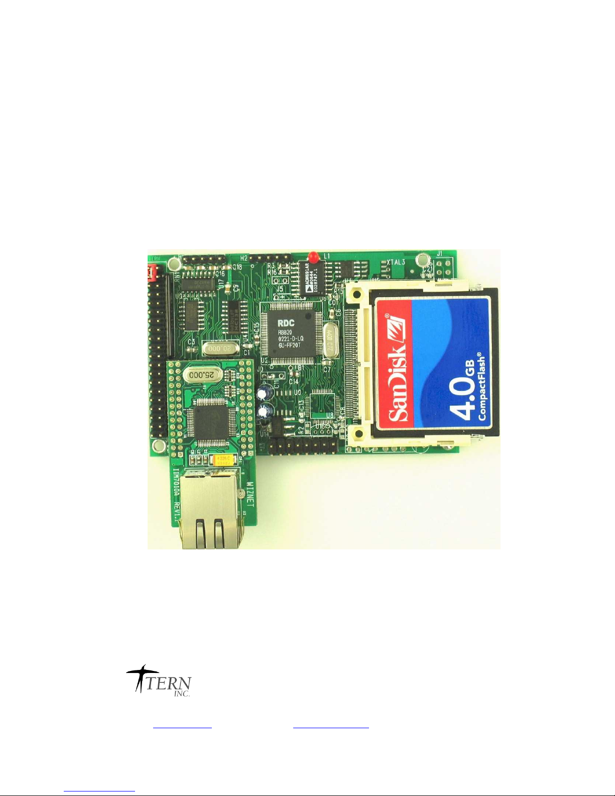
Measuring 3.6 x 2.3 inches, the CAN-Engine™ (CANE) is a high performance, low cost, C/C++ programmable
controller. It is intended for networking application including industrial process control, high-speed data acquisition,
and especially ideal for OEM applications.
The CANE can use any one of these 3 16-bit CPU chips: 40 MHz AM186ES(5V), or 40 MHz RDC R8820(5V) or
80MHz RDC R1120(3.3V).
An Fast Ethernet Module can be installed to provide 100M Base-T network connectivity. This Ethernet module has
a hardware LSI TCP/IP stack. It implements TCP/IP, UDP, ICMP and ARP in hardware, supporting internet
protocol DLC and MAC. It has 16KB internal transmit and receiving buffer which is mapped into host processor’s
direct memory. The host can access the buffer via high speed DMA transfers. The hardware Ethernet module
releases internet connectivity and protocol processing from the host processor, which represents a huge improvement
over software-based TCP/IP stacks. No processor cycles are used to track packet transmission/retransmission,
timeouts, etc. The resulting system can easily handle transmissions in the 100K bytes per second+ range in real
world applications. It supports 4 independent stack connections simultaneously at a 4Mbps protocol processing
speed. An RJ45 8-pin connector is on-board for connecting to 10/100 Base-T Ethernet network. Software libraries
and demo project are available for Ethernet connectivity.
A Controller Area Network (CAN) controller (SJA1000, 20 MHz clock) and CAN bus tranceiver is available. It
supports network baud rates up to 1M-bit per second. Software drivers allow access to all CAN controller registers,
as well as a buffering software layer.
The CANE features fast execution times through 16-bit ACTF Flash (256 KW) and battery-backed SRAM (256
KW). It also includes 3 timers, PWMs, 20+ PIOs, 512-byte serial EEPROM, two UARTs, 3 timer/counters, and a
watchdog timer. The three 16-bit timers can be used to count or time external events, up to 10 MHz, or to generate
non-repetitive or variable-duty-cycle waveforms as PWM outputs. The PIO pins are multifunctional and user
programmable.
A serial real timer clock (DS1337, Dallas) is a low power clock/calendar with two time-of-day alarms and a
programmable square-wave output.
Two RS232 channels of full-duplex asynchronous receivers and transmitters are on-board. The UARTs incorporate
9-bit mode for multi-processor communications.
A 16-bit parallel ADC (AD7655, 0-5V) supports ultra high-speed (1 MHz conversion rate) analog signal acquisition.
The AD7655 contains two low noise, high bandwidth track-and-hold amplifiers that allow simultaneous sampling on
two channels. Each track-and hold amplifier has a multiplexer in front to provide a total of 4 channels analog inputs.
The parallel ADC achieves high throughput by requiring only two CPU I/O operations (one start, one read) to
complete a 16-bit ADC reading. With a precision external 2.5V reference, the ADC accepts 0-5V analog inputs at
16-bit resolution of 0-65,535.
The CANE supports low cost, removable, up to 2 GB mass storage CompactFlash cards with onboard CompactFlash
interface. User can store and transfer large amounts of data with a PC, via a CF card with TERN’s FAT filesystem
software support.
The CANE can be powered by USB, or regulated 5V, or unregulated 9V DC power with on-board 5V regulator
installed.
The CANE provides a true 16-bit data bus for SRAM, Flash, ADC, Ethernet, and a J1 20x2 expansion header. The
CANE is an ideal upgrade for the A-Engine, V25-Engine, 386-Engine, or R-Engine providing increased reliability,
networking functionality, and performance. They have the similar mechanical dimensions, pin outs, software drivers,
and both are programmed using Paradigm C++ TERN Edition Evaluation Kit (EV-P) or Development Kit (DV-P).
Page 4
Chapter 1: Introduction CAN-Engine
1-2
The CANE can be integrated into an OEM product as a processor core component. It also can be used to build a
smart sensor, or can act as a node in a distributed microprocessor system.
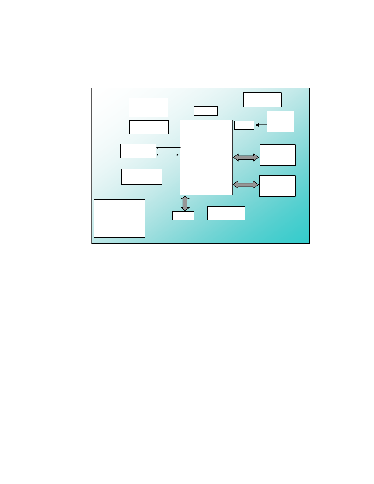
Am186ES
R8820/R1120
CPU
40/80MHz
DMA(2)
16-Bit Timers(3)
Ext. Interrupts(8)
32 I/O lines
PWM/PWD
16-bit Ext. data bus
691
U6
EEPROM U7
512 BYTES
FLASH
512 KB 16-bit
U1
RS232 drivers
SER0+SER1
SDA P11
SDL P12
J1 & J2
100M BaseT
Ethernet
JP1+JP2
4 ch. 16-bit
AD7655
U8
RTC
U15
Low drop 5V
regulators for USB
U0+U01
Or
Linear 5V regulators
LM7805
SRAM
128KB or 512 KB
16-bit
U3
J9
watchdog
enable
CAN-Engine
CAN
U5
CompactFlash
U11
D0..D15
D0..D15
Figure 1.1 Functional block diagram of the CAN-Engine
The CANE supports on-board 512 KB 16-bit Flash and up to 512 KB 16-bit battery-backed SRAM. The on-board
ACTF Flash has a protected boot loader and can be easily programmed in the field via serial link. Users can
download a kernel into the Flash for remote debugging. With the DV-P Kit support, user application codes can be
easily field-programmed into and run out of the Flash.
A 512-byte serial EEPROM is included on-board. Two DMA-driven serial ports from the Am186ES support highspeed, reliable serial communication at a rate of up to 115,200 baud. All serial ports support 8-bit and 9-bit
communication.
There are three 16-bit programmable timers/counters and a watchdog timer. Two timers can be used to count or time
external events, at a rate of up to 10 MHz, or to generate non-repetitive or variable-duty-cycle waveforms as PWM
outputs. Pulse Width Demodulation (PWD), a distinctive feature, can be used to measure the width of a signal in
both its high and low phases. It can be used in many applications, such as bar-code reading.
The EE has 32 user-programmable, multifunctional I/O pins from the CPU. Schmitt-trigger inverters are provided
for six external interrupt inputs, to increase noise immunity and transform slowly-changing input signals into fastchanging and jitter-free signals. A supervisor chip with power failure detection, a watchdog timer, an LED, and
expansion ports are on-board.
Page 5
CAN-Engine Chapter 1: Introduction
1-3
Features:
• 3.6 x 2.3 x 1”, 200 mA at 5V for 80 MHz
• 40 or 80 MHz, 16-bit CPU, program in C/C++
• 256 KW 16-bit Flash, 256 KW 16-bit SRAM, 512 bytes EE
• Controller Area Network (CAN2.0B)
• 20+ TTL I/Os, Real-time clock, 2 serial ports, PWM, counters
• 4 ch 16-bit parallel high speed ADC (AD7655)
• Hardware TCP/IP stack for 100M Base-T Ethernet
• CompactFlash card with FAT file system support
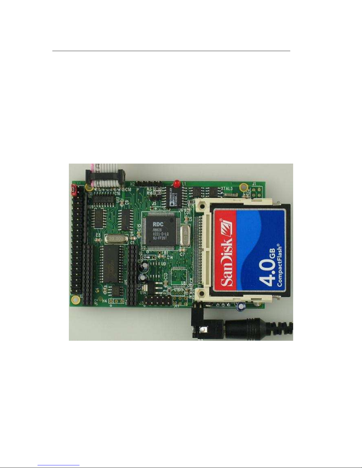
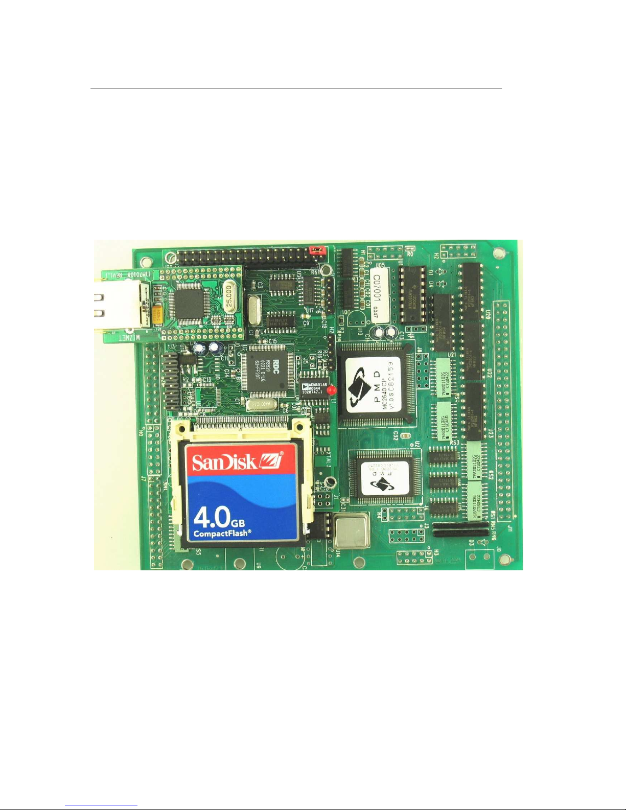
1.2 Physical Description
The physical layout of the CAN-Engine is shown in Figure 1.2.
Figure 1.2 Physical layout of the CAN-Engine
Page 6
Chapter 1: Introduction CAN-Engine
1-4
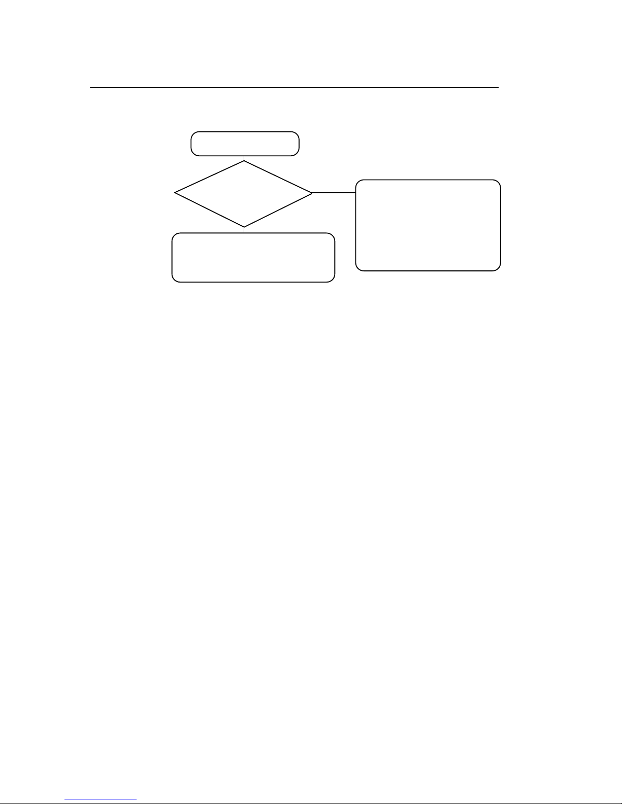
Figure 1.3 Flow chart for ACTF operation
The “ACTF boot loader” resides in the top protected sector of the 512KB on-board Flash chip (29F400).
By default, in the factory, before shipping, the DEBUG kernel (EE40_115.hex) is pre-loaded
in the Flash starting at 0xFA000, and the RED STEP2 jumper is installed, ready for
Paradigm C++ debugger. User does not need to download a DEBUG kernel to start with.
At power-on or RESET, the “ACTF” will check the STEP 2 jumper. If STEP 2 jumper is not installed, the ACTF
menu will be sent out from serial port0 at 19200 baud for a CANE 40MHz, or 9600 baud for a CANE 80MHz.
If the STEP 2 jumper is install ed, the “jump address” located in the on-board serial EE will be read out and then
jump to that address. A DEBUG kernel “EE40_115.hex” for the CANE 40MHz or “EE80_115.hex” for the CANE
80MHz can be downloaded, residing in “0xFA000” of the 512KB on-board flash chip.
The “EE84_115.hex can also be downloaded into a CANE 80MHz for easier running all demo projects, which are
designed for running 40MHz.
Power On or Reset
YES
Go to Application Code CS:IP
STEP 2
ACTF menu sent out through ser0
STEP 1
Step 2 jumper
NO
set?
CS:IP in EEPROM:
0x10=CS high byte
0x11=CS low byte
0x12=IP high byte
0x13=IP low byte
at 19200/9600 baud(EE40/80)
Page 7
CAN-Engine Chapter 1: Introduction
1-5
1.3 CAN-Engine Programming Overview
Steps for product development:
Preparation for Debugging(DONE in Factory !)
• Connect board to PC via RS-232 link, 19,200, 8, N, 1
• Power on without STEP 2 jumper installed
• ACTF menu should be sent to PC terminal
• Use “D” command to download “L_TDREM.HEX” in SRAM
• “G04000” to run “L_TDREM”
•
Download “c:
\
tern\186\rom\ae86\E
E40_115.HEX” to Flash
• “GFA000” to setup EEPROM and run remote debugger
• Install the STEP2 jumper (J2.38-40)
• Power-on or reset, Ready for Remote debugger
STEP 2:
Standalone Field Test
8888”G08000” setup EEPROM Jump Address, points to
application code resides in battery backed SRAM
8888Install STEP2 jumper, then power on
8888 Application program running in battery-backed SRAM
(Battery lasts 3
-
5 years under normal conditions.)
• Start Paradigm C++, run “led.ide” or “test.ide”
• Download code to target SRAM.
• Edit, compile, link, locate, download, and remote-debug
STEP 1:
Debugging
STEP 3:
DV-P Kit
• Generate application HEX file with DV-P and ACTF Kit
• ACTF “D” to download “L_29F400.HEX” into SRAM
• Download application HEX file into FLASH
• Modify EEPROM jump address to 0x80000
• Set STEP2 jumper
Production
There is no ROM socket on the board. The user’s application program must reside in SRAM for debugging in
STEP1, reside in battery-backed SRAM for the standalone field test in STEP2, and finally be programmed into the
on-board Flash for a complete product. For production, the user must produce an ACTF-downloadable HEX file for
the application, based on the DV-P Kit. The “STEP2” jumper (J2 pins 38-40) must be installed for every productionversion board.
Step 1 settings
In order to talk to CANE with Paradign C++, the CANE must meet these requirements:
1) EE40_115.HEX or EE80_115.HEX must be pre-loaded into Flash starting address 0xfa000.
2) The SRAM installed must be large enough to hold your program.
Page 8
Chapter 1: Introduction CAN-Engine
1-6
For a 128K SRAM, the physical address is 0x00000-0x01ffff
For a 512K SRAM, the physical address is 0x00000-0x07ffff
3) The on-board CANE must have a Jump Address of 0xfa000.
4) The STEP2 jumper must be installed on J2 pins 38-40.
For further information on programming the CAN-Engine, refer to the manual on the TERN CD under:
tern_docs\manuals\software_kit.pdf.
The CANE works with most TERN expansion boards including the P50, P100, P300, MotionC, MMC, and Eye0.
Figure 1.4 CAN-Engine is installed on the top of the MotionC-P.
Page 9

CAN-Engine Chapter 2: Installation
2-1
Chapter 2: Installation
2.1 Software Installation
Please refer to the “software_kit.pdf” technical manual on the TERN installation CD, under
tern_docs\manual\software_kit.pdf, for information on installing software.
2.2 Hardware Installation
Hardware installation consists primarily of connecting the microcontroller to your PC.
2.2.1 Connecting to the PC
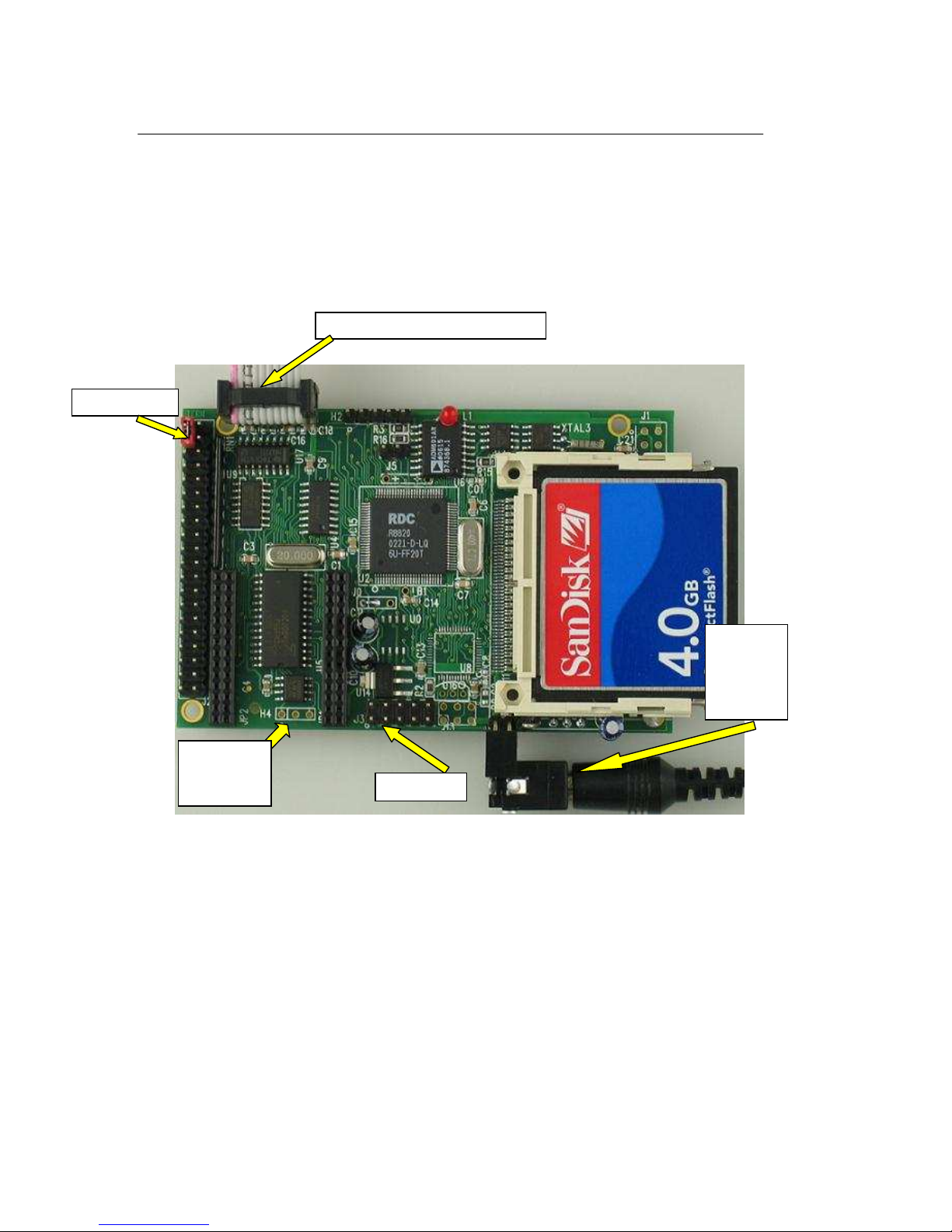
The following diagram (Fig 2.1) provides the location of the debug serial port and the power jack. The
controller is linked to the PC via a serial cable (DB9-IDE) which is supplied with TERN’s EV-P / DV-P
Kits.
The controller communicates through SER0 by default. Install the 5x2 IDE connector on the SER0 5x2 pin
header. IMPORTANT: Note that the red side of the cable must point to pin 1 of the SER0 header. The
DB9 connector should be connected to one of your PC's COM Ports (COM1 or COM2).
2.2.2 Powering-on the CAN-Engine™
By factory default setting:
1) The RED STEP2 Jumper is installed. (Default setting in factory)
2) The DEBUG kernel is pre-loaded into the on-board flash starting at address of 0xFA000. (Default setting
in factory)
3) The EEPROM is set to jump address of 0xFA000. (Default setting in factory)
Connect +9-12V DC to the DC power terminal. The DC power jack adapter is center negative.
The on-board LED should blink twice and remain on, indicating the debug kernel is running and ready to
communicate with Paradigm C++ TERN Edition for programming and debugging.
(See next page for connection diagram).
Overview
• Connect PC-IDE serial cable:
For debugging (STEP 1), place IDE connector on SER0 (H1)
with red edge of cable at pin 1. This DEBUG cable is a 10-pin
IDE to DB9 cable, made by TERN (See Appendix D).
• Connect wall transformer:
Connect 9V wall transformer to power and plug into power jack
using power jack adapter supplied with EV-P/DV-P Kit
Page 10
Chapter 2: Installation CAN-Engine
2-2
2.2.3 Connecting the CAN-Engine™
The proper connections required to debug the board (through Paradigm software).
H1 (Ser 0) is a 5x1 pin header. Use the back row of the IDE cable’s female header to connect to H1. (See
Appendix D)
Figure 2.1: Debug Cable (Ser0), Power Plug, and Step 2 Jumper shown
NOTE: Remember to watch for the “double blink” off the LED. This indicates the Debug Kernel has
been loaded with the jump address pointing to it. This is mandatory to commence downloading code
through the Paradigm environment.
Step 2 Jumper
H1 (Ser 0)
IDE-DB9
Debug
Cable
9-12 Volt
Power
plug
(Center
Negative)
CAN Port
CAN
Termination
Resistor.
Page 11

CAN-Engine Chapter 3: Hardware
3-1
Chapter 3: Hardware
3.1 Am186ES/R8820/R1120 - Introduction
The Am186ES is based on industry-standard x86 architecture. The Am186ES controllers uses 16-bit
external data bus, are higher-performance, more integrated versions of the 80C188 microprocessors which
uses 8-bit external data bus. In addition, the Am186ES has new peripherals. The on-chip system interface
logic can minimize total system cost. The Am186ES has two asynchronous serial ports, 32 PIOs, a
watchdog timer, additional interrupt pins, a pulse width demodulation option, DMA to and from serial
ports, a 16-bit reset configuration register, and enhanced chip-select functionality.
R8820 is a drop-in replacement 5V, 40MHz chip for the AM186ES. Connecting J0.1=J0.2.
R1100 is a 80MHz, 3.3V chip can be installed on the E-Engine with J0.2=J0.3.
By default, the E-Engine uses 5V 40 MHz R8820 and low power 55-70 ns SRAM with battery backup.
Optional 3.3V 80 MHz R1120 can be installed.
At 80 MHz, the low power 55 ns SRAM with battery backup works fine but will not be able to support
DMA operation.
A fast 10/15/25 ns SRAM (Not low power) can be used to support zero wait state and DMA operation at 80
MHz, but the backup battery will be drain in few days.
There are three pads on the PCB for battery. One pads is ground, and the other two pads allowing a 3V
backup lithium battery is installed in two different positions:
1) The battery’s positive lead is installed in the pad which is away from the RTC, supporting the RTC only.
No battery backup for the SRAM.
2) The battery’s positive lead is installed in the pad which is closer to the RTC, supporting both RTC and
SRAM.
In the future, when the fast (10 ns) and low standby power SRAM is available, then 80 MHz E-Engine can
have both RTC and SRAM with battery backup plus the DMA, zero wait state operation.
User can use sample program c:\tern\186\samples\ee\rdc_id.c to read the ID register (0xfff4), in order to
identify RDC CPU type.
R1100=0xC5D9, R1120=0x85D9, R8820/30=0x04D9(xxD9)
3.2 Am186ES – Features
3.2.1 Clock and crystal
Due to its integrated clock generation circuitry, the Am186ES microcontroller allows the use of a times-one
crystal frequency. The design achieves 40 MHz CPU operation, while using a 40 MHz crystal.
The system CLKOUTA signal is routed to J1 pin 4, default 40 MHz for EE40.
CLKOUTA remains active during reset and bus hold conditions. The initial function ae_init(); disables
CLKOUTA and CLKOUTB with clka_en(0); and clkb_en(0);
You may use clka_en(1); to enable CLKOUTA=CLK=J1 pin 4.
The R8820 uses a 40 MHz crystal.
By default the 3.3V R1120 uses a 20 MHz crystal. The CPU speed is software programmable with the PLL.
At power-on, the on-board ACTF Flash programs the R1120 running at 20 MHz system clock, so a 9600
baud (instead 19,200 baud) is used for ACTF Manu.
Three debug kernels are available:
Page 12

Chapter 3: Hardware CAN-Engine
3-2
c:\tern\186\rom\ae86\EE40_115.hex,
c:\tern\186\rom\ae86\EE80_115.hex,
c:\tern\186\rom\ae86\EE84_115.hex.
The EE40_115.hex will run the R8820 at 40 MHz, and the EE80_115.hex will run the R1120 at 80 MHz.
The EE84_115.hex will run the R1120 at 40 MHz
By default, the EE40_115.hex is pre-programmed for the 40 MHz CAN-Engine.
User can use software to setup the CPU speed:
outport(0xfff8,0x0103); // PLLCON, 20MHz crystal, 0103=40 MHz, 0107=80MHz
3.2.2 External Interrupts and Schmitt Trigger Input Buffer
There are eight external interrupts: INT0-INT6 and NMI.
/INT0, J2 pin 8, free to use.
/INT1, J2 pin 6, free to use.
INT2, J2 pin 19, RTC DS1337 alarm
/INT3, J2 pin 21, CAN
/INT4, J2 pin 33, used by 100M BaseT Ethernet
INT5=P12=DRQ0, J2 pin 5, used for LED/EE/HWD
INT6=P13=DRQ1, J2 pin 11, Free to use.
/NMI, J2 pin 7
Some of external interrupt inputs, /INT0, 1, 3, 4 and /NMI, are buffered by Schmitt-trigger inverters (U9,
74HC14), in order to increase noise immunity and transform slowly changing input signals to fast changing
and jitter-free signals. As a result of this buffering, these pins are capable of only acting as input.
These buffered external interrupt inputs require a falling edge (HIGH-to-LOW) to generate an interrupt.
The CAN-Engine uses vector interrupt functions to respond to external interrupts. Refer to the Am186ES
User’s manual for information about interrupt vectors.
3.2.3 Asynchronous Serial Ports
The Am186ES CPU has two asynchronous serial channels: SER0 and SER1. Both asynchronous serial
ports support the following:
• Full-duplex operation
• 7-bit, 8-bit, and 9-bit data transfers
• Odd, even, and no parity
• One stop bit
• Error detection
• Hardware flow control
• DMA transfers to and from serial ports
• Transmit and receive interrupts for each port
• Multidrop 9-bit protocol support
• Maximum baud rate of 1/16 of the CPU clock speed
• Independent baud rate generators
The software drivers for each serial port implement a ring-buffered DMA receiving and ring-buffered
interrupt transmitting arrangement. See the samples files s1_echo.c and s0_echo.c.
Page 13

CAN-Engine Chapter 3: Hardware
3-3
Important Note: For 80MHz CAN Engine, DMA functions are not available when by default low power 55
ns SRAM is installed. If install a 25 ns SRAM, 80MHz CANE can have all DMA functions, but it will
drain the backup battery fast. Two battery positive pads allowing the battery be installed:
1) Support both RTC and low power SRAM, or
2) Support only RTC.
3.2.4 Timer Control Unit
The timer/counter unit has three 16-bit programmable timers: Timer0, Timer1, and Timer2.
Timer0 and Timer1 are connected to external pins:
Timer0 output = P10 = J2 pin 12
Timer0 input = P11 = U7 EE pin 5
Timer1 output = P1 = J2 pin 29
Timer1 input = P0 = J2 pin 20
Timer0 input P11 is used and shared by on-board EE, LED, and HitWD, not recommended for other
external use.
The timer can be used to count or time external events, or can generate non-repetitive or variable-duty-cycle
waveforms.
Timer2 is not connected to any external pin. It can be used as an internal timer for real-time coding or timedelay applications. It can also prescale timer 0 and timer 1 or be used as a DMA request source.
The maximum rate at which each timer can operate is 10 MHz, since each timer is serviced once every
fourth clock cycle. Timer output takes up to six clock cycles to respond to clock or gate events. See the
sample programs timer02.c and ae_cnt1.c in the tern\186\samples\ae directory.
3.2.5 PWM outputs and PWD
The Timer0 and Timer1 outputs can also be used to generate non-repetitive or variable-duty-cycle
waveforms. The timer output takes up to 6 clock cycles to respond to the clock input. Thus the minimum
timer output cycle is 25 ns x 6 = 150 ns (at 40 MHz).
Each timer has a maximum count register that defines the maximum value the timer will reach. Both Timer0
and Timer1 have secondary maximum count registers for variable duty cycle output. Using both the primary
and secondary maximum count registers lets the timer alternate between two maximum values.
MAX. COUNT A
MAX. COUNT B
Pulse Width Demodulation can be used to measure the input signal’s high and low phases on the /INT2=J2
pin 19.
3.2.6 Power-save Mode
The power-save mode of the Am186ES reduces power consumption and heat dissipation, thereby extending
battery life in portable systems. In power-save mode, operation of the CPU and internal peripherals
continues at a slower clock frequency. When an interrupt occurs, it automatically returns to its normal
operating frequency.
Page 14

Chapter 3: Hardware CAN-Engine
3-4
3.3 Am186ES PIO lines
The Am186ES has 32 pins available as user-programmable I/O lines. Each of these pins can be used as a
user-programmable input or output signal, if the normal shared function is not needed. A PIO line can be
configured to operate as an input or output with or without a weak pull-up or pull-down, or as an open-drain
output. A pin’s behavior, either pull-up or pull-down, is pre-determined and shown in the table below.
After power-on/reset, PIO pins default to various configurations. The initialization routine provided by
TERN libraries reconfigures some of these pins as needed for specific on-board usage, as well. These
configurations, as well as the processor-internal peripheral usage configurations, are listed below in Table
3.1.
PIO Function Power-On/Reset status CAN-Engine Pin No. CAN-Engine Initial
P0 Timer1 in Input with pull-up J2 pin 20 Input with pull-up
P1 Timer1 out Input with pull-down J2 pin 29 Input with pull-down
P2 /PCS6/A2 Input with pull-up J2 pin 24 Input with pull-up
P3 /PCS5/A1 Input with pull-up J2 pin 15 Input with pull-up
P4 DT/R Normal J2 pin 38 Input with pull-up Step 2
P5 /DEN/DS Normal J2 pin 30 Input with pull-up
P6 SRDY Normal J2 pin 35 Input with pull-down
P7 A17 Normal U3 pin 22 A17
P8 A18 Normal U3 pin 23 A18
P9 A19 Normal J2 pin 10 A19
P10 Timer0 out Input with pull-down J2 pin 12 Input with pull-down
P11 Timer0 in Input with pull-up U7 EE pin 5 Input with pull-up
P12 DRQ0/INT5 Input with pull-up J2 pin 5 Output for LED/EE/HWD
P13 DRQ1/INT6 Input with pull-up J2 pin 11 Input with pull-up
P14 /MCS0 Input with pull-up J2 pin 37 Input with pull-up(ET)
P15 /MCS1 Input with pull-up J2 pin 23 Input with pull-up
P16 /PCS0 Input with pull-up J1 pin 19 /PCS0
P17 /PCS1 Input with pull-up J2 pin 13 CAN, ADC, CF select
P18 CTS1/PCS2 Input with pull-up J2 pin 22 Input with pull-up
P19 RTS1/PCS3 Input with pull-up J2 pin 31 Input with pull-up
P20 RTS0 Input with pull-up J2 pin 27 Input with pull-up
P21 CTS0 Input with pull-up J2 pin 36 Input with pull-up
P22 TxD0 Input with pull-up J2 pin 34 TxD0
P23 RxD0 Input with pull-up J2 pin 32 RxD0
P24 /MCS2 Input with pull-up J2 pin 17 Input with pull-up
P25 /MCS3 Input with pull-up J2 pin 18 Input with pull-up
P26 UZI Input with pull-up J2 pin 4 Input with pull-up*
P27 TxD1 Input with pull-up J2 pin 28 TxD1
P28 RxD1 Input with pull-up J2 pin 26 RxD1
P29 /CLKDIV2 Input with pull-up J2 pin 3 Input with pull-up*
P30 INT4 Input with pull-up J2 pin 33 Input with pull-up
P31 INT2 Input with pull-up J2 pin 19 Input with pull-up
* Note: P26 and P29 must NOT be forced low during power-on or reset.
Table 3.1 I/O pin default configuration after power-on or reset
Page 15

CAN-Engine Chapter 3: Hardware
3-5
Three external interrupt lines are not shared with PIO pins:
INT0 = J2 pin 8
INT1 = J2 pin 6
INT3 = J2 pin 21
The 32 PIO lines, P0-P31, are configurable via two 16-bit registers, PIOMODE and PIODIRECTION. The
settings are as follows:
MODE PIOMODE reg. PIODIRECTION reg. PIN FUNCTION
0 0 0 Normal operation
1 0 1 INPUT with pull-up/pull-down
2 1 0 OUTPUT
3 1 1 INPUT without pull-up/pull-down
CAN-Engine initialization on PIO pins in ae_init() is listed below:
outport(0xff78,0xe73c); // PDIR1, TxD0, RxD0, TxD1, RxD1, P16=PCS0, P17=PCS1=PPI
outport(0xff76,0x0000); // PIOM1
outport(0xff72,0xec7b); // PDIR0, P12,A19,A18,A17,P2=PCS6=RTC
outport(0xff70,0x1000); // PIOM0, P12=LED
The C function in the library ae_lib can be used to initialize PIO pins.
void pio_init(char bit, char mode);
Where bit = 0-31 and mode = 0-3, see the table above.
Example: pio_init(12, 2); will set P12 as output
pio_init(1, 0); will set P1 as Timer1 output
void pio_wr(char bit, char dat);
pio_wr(12,1); set P12 pin high, if P12 is in output mode
pio_wr(12,0); set P12 pin low, if P12 is in output mode
unsigned int pio_rd(char port);
pio_rd (0); return 16-bit status of P0-P15, if corresponding pin is in input mode,
pio_rd (1); return 16-bit status of P16-P31, if corresponding pin is in input mode,
Some of the I/O lines are used by the CAN-Engine system for on-board components (Table 3.2). We
suggest that you not use these lines unless you are sure that you are not interfering with the operation of
such components (i.e., if the component is not installed).
You should also note that the external interrupt PIO pins INT2, 4, 5, and 6 are not available for use as
output because of the inverters attached. The input values of these PIO interrupt lines will also be inverted
for the same reason. As a result, calling pio_rd to read the value of P31 (INT2) will return 1 when pin 19
on header J2 is pulled low, with the result reversed if the pin is pulled high.
Signal Pin Function
P14 /MCS0 100M BaseT Ethernet
P4 /DT STEP2 jumper
P11 Timer0 input Shared with RTC, EE data input
P12 DRQ0/INT5 Output for LED or U7 serial EE clock or Hit watchdog
P17 /PCS1 CAN, ADC
P22 TxD0 Default SER0 debug
Page 16

Chapter 3: Hardware CAN-Engine
3-6
Signal Pin Function
P23 RxD0 Default SER0 debug
/INT4 J2 pin 33 Ethernet interrupt, if U8 is installed
Table 3.2 I/O lines used for on-board components
3.4 I/O Mapped Devices
3.4.1 I/O Space
External I/O devices can use I/O mapping for access. You can access such I/O devices with inportb(port) or
outportb(port,dat). These functions will transfer one byte or word of data to the specified I/O address. The
external I/O space is 64K, ranging from 0x0000 to 0xffff.
The default I/O access time is 15 wait states. You may use the function void io_wait(char wait) to define the
I/O wait states from 0 to 15. The system clock is 25 ns ( or 50 ns), giving a clock speed of 40 MHz (or 20
MHz). Details regarding this can be found in the Software chapter, and in the Am186ES User’s Manual.
Slower components, such as most LCD interfaces, might find the maximum programmable wait state of 15
cycles still insufficient. Due to the high bus speed of the system, some components need to be attached to
I/O pins directly.
For details regarding the chip select unit, please see Chapter 5 of the Am186ES User’s Manual.
The table below shows more information about I/O mapping.
I/O space Select Location Usage
0x0000-0x00ff /PCS0 J1 pin 19=P16 USER*
0x0100-0x0103 /PCS1 J2 pin 13=P17 U4 pin 4-5
0x0200-0x02ff /PCS2 J2 pin 22=CTS1 USER
0x0300-0x03ff /PCS3 J2 pin 31=RTS1 USER
0x0400-0x04ff /PCS4 Reserved
0x0500-0x05ff /PCS5 J2 pin 15=P3 USER
0x0600-0x06ff /PCS6 J2 pin 24=P2 USER
*PCS0 may be used for other TERN peripheral boards.
To illustrate how to interface the CAN-Engine with external I/O boards, a simple decoding circuit for
interfacing to an 82C55 parallel I/O chip is shown in Figure 3.1.
/WR
/RD
/SEL20
A0
A1
D0-D7
/CS
/WR
/RD
82C55
RST
P00-P07
P10-P17
P20-P27
1
/PCS0
A7
6
VCC
4
3
2
5
A5
A6
/SEL20
/SELF0
/SELC0
/SELA0
/SEL80
/SEL60
/SEL40
14
13
12
11
10
9
7
NC
15
74HC138
C
A
B
G2A
G2B
G1
Y2
Y3
Y4
Y5
Y6
Y7
Y1
Y0
Figure 3.1 Interface to external I/O devices
Page 17

CAN-Engine Chapter 3: Hardware
3-7
The function ae_init() by default initializes the /PCS0 line at base I/O address starting at 0x00. You
can read from the 82C55 with inportb(0x020) or write to the 82C55 with outportb(0x020,dat). The call to
inportb(0x020) will activate /PCS0, as well as putting the address 0x00 over the address bus. The decoder
will select the 82C55 based on address lines A5-7, and the data bus will be used to read the appropriate data
from the off-board component.
3.5 Other Devices
A number of other devices are also available. Some of these are optional, and might not be installed on the
particular controller you are using. For a discussion regarding the software interface for these components,
please see the Software chapter.
3.5.1 On-board Supervisor with Watchdog Timer
The MAX691/LTC691 (U6) is a supervisor chip. With it installed, the CAN-Engine has several functions:
watchdog timer, battery backup, power-on-reset delay, power-supply monitoring, and power-failure
warning. These will significantly improve system reliability.
Watchdog Timer
The watchdog timer is activated by setting a jumper on J5 of the CAN-Engine. The watchdog timer
provides a means of verifying proper software execution. In the user's application program, calls to the
function hitwd() (a routine that toggles the P12=HWD pin of the MAX691) should be arranged such that
the HWD pin is accessed at least once every 1.6 seconds. If the J5 jumper is on and the HWD pin is not
accessed within this time-out period, the watchdog timer pulls the WDO pin low, which asserts /RESET.
This automatic assertion of /RESET may recover the application program if something is wrong. After the
CAN-Engine is reset, the WDO remains low until a transition occurs at the WDI pin of the MAX691. When
controllers are shipped from the factory the J5 jumper is off, which disables the watchdog timer.
The Am186ES has an internal watchdog timer. This is disabled by default with ae_init().
Page 18

Chapter 3: Hardware CAN-Engine
3-8
Figure 3.2 Location of watchdog timer enable jumper
Power-failure Warning
The supervisor supports power-failure warning and backup battery protection. When power failure is
sensed by the PFI=J1.11, pin 9 of the MAX691 (lower than 1.3 V), the PFO is low. The PFI pin 9 of 691 is
directly shorted to VCC by default. In order to use PFI externally, cut the trace and bring the PFI signal out.
You may design an NMI service routine to take protect actions before the +5V drops and processor dies.
The following circuit shows how you might use the power-failure detection logic within your application.
47K
2K
PFI, pin 9 of MAX691
(1.3 V min)
(8.35 V min)
9-14 V
C?
VCC = +5V
Using the supervisor chip for power failure detection
Battery Backup Protection
The backup battery protection protects data stored in the SRAM and RTC. The battery-switch-over circuit
compares VCC to VBAT (+3 V lithium battery positive pin), and connects whichever is higher to the
VRAM (power for SRAM and RTC). Thus, the SRAM and the real-time clock are backed up. In normal
J5 WatchDog
Page 19

CAN-Engine Chapter 3: Hardware
3-9
use, the lithium battery should last about 3-5 years without external power being supplied. When the
external power is on, the battery-switch-over circuit will select the VCC to connect to the VRAM.
3.5.2 EEPROM
A serial EEPROM of 512 bytes (24C04), or optional 2K bytes (24C16) can be installed in U7. The CANEngine uses the P12=SCL (serial clock) and P11=SDA (serial data) to interface with the EEPROM. The
EEPROM can be used to store important data such as a node address, calibration coefficients, and
configuration codes. It typically has 1,000,000 erase/write cycles. The data retention is more than 40 years.
EEPROM can be read and written by simply calling the functions ee_rd() and ee_wr().
A range of lower addresses in the EEPROM is reserved for TERN use. Details regarding which addresses
are reserved, and for what purpose, can be found in Appendix E of this manual.
3.5.3 AD7655, 16-bit parallel high speed ADC
The unique 16-bit parallel ADC (AD7655, 0-5V) supports ultra high-speed (1 MHz conversion rate) analog
signal acquisition. The AD7655 contains two low noise, high bandwidth track-and-hold amplifiers that
allow simultaneous sampling on two channels. Each track-and hold amplifier has a multiplexer in front to
provide a total of 4 channels analog inputs. The parallel ADC achieves very high throughput by requiring
only two CPU I/O operations (one start, one read) to complete a 16-bit ADC reading. With a precision
external 2.5V reference, the ADC accepts 0-5V analog inputs at 16-bit resolution of 0-65,535.
See sample program \tern\186\samples\ee\ee_ad.c for details on reading the ADC. The sample program is
also included in the pre-built sample project; \tern\186\samples\ee\ee.ide.
Refer to the data sheet for additional specifications; \tern_docs\parts\ad7655.pdf.
3.5.4 CAN
The CAN-Engine supports an on-board Controller Area Network (CAN) controller(SJA1000, Philips). It
supports network baud rates up to 1M-bit per second. Software drivers allow access to all CAN controller
registers, as well as a buffering software layer.
The CAN bus is a balanced (differential) 2-wire interface running over either a Shielded Twisted Pair
(STP), Un-shielded Twisted Pair (UTP), or Ribbon cable.
CAN Bus Electrical Interface Circuit
Page 20

Chapter 3: Hardware CAN-Engine
3-10
A number of different data rates are defined, with 1Mbps (Bits per second) being the top end, and 10kbps
the minimum rate. Cable length depends on the data rate used. Normally all the devices in a system transfer
uniform and fixed bit-rates. The maximum line length is 1Km, 40 meters at 1Mbps. Termination resistors
are used at each end of the cable. The worst-case transmission time of an 8-byte frame with an 11-bit
identifier is 134 bit times (that's 134 microseconds at the maximum baud rate of 1Mbits/sec).
The CAN Bus interface uses an asynchronous transmission scheme controlled by start and stop bits at the
beginning and end of each character. This interface is used, employing serial binary interchange.
Information is passed from transmitters to receivers in a data frame. The data frame is composed of an
Arbitration field, Control field, Data field, CRC field, ACK field. The frame begins with a 'Start of frame'
[SOF], and ends with an 'End of frame' [EOF] space. The data field may be from 0 to 8 bits.
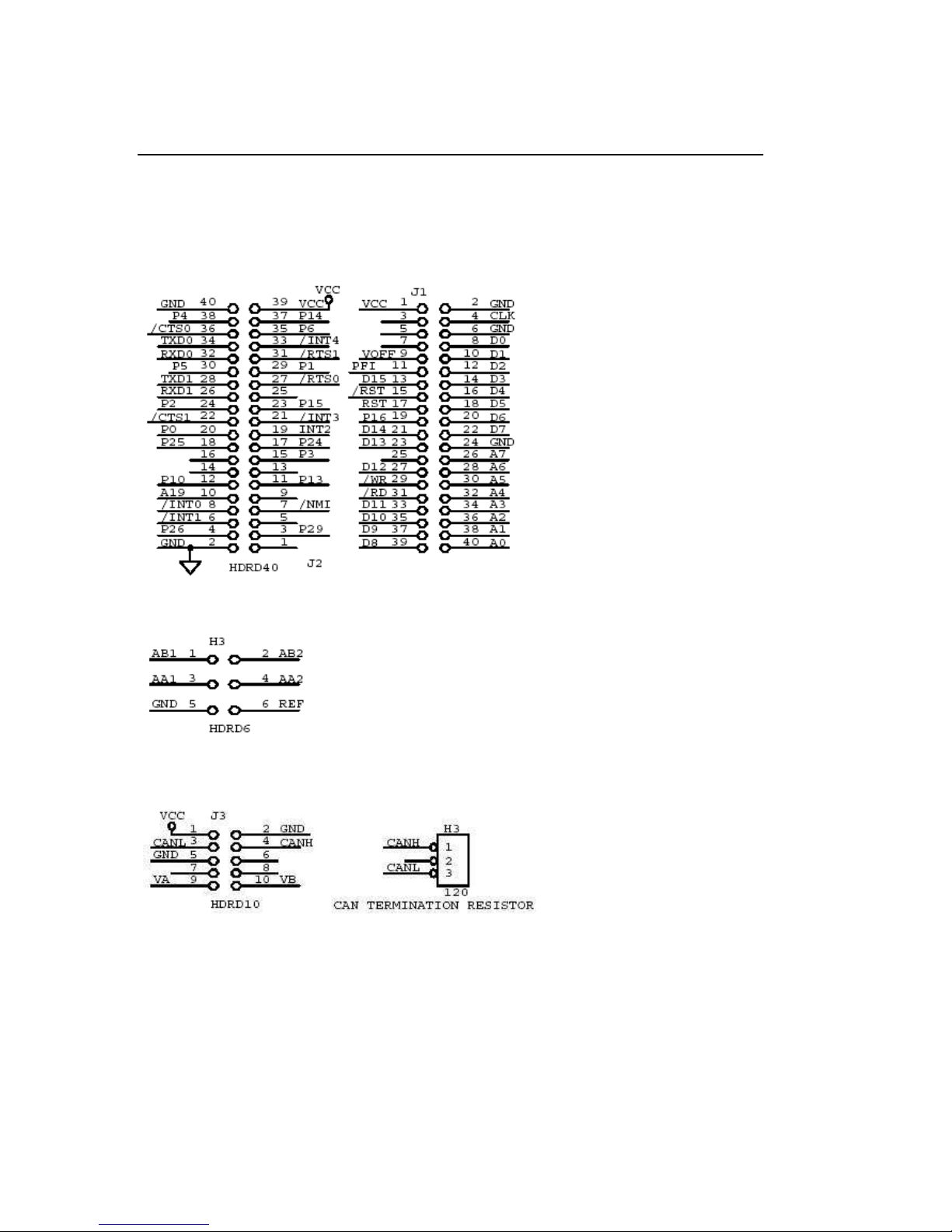
The CAN bus pinout on J3 is shown below. It is a compact 0.1” spacing 3x2 pin header. User can use a
IDE10-DB9 flat cable from TERN to connect CAN signals to an external standard DB9 CAN connector in
the field.
3.5.5 100 MHz BaseT Ethernet
An WizNet™ Fast Ethernet Module can be installed to provide 100M Base-T network connectivity. This
Ethernet module has a hardware LSI TCP/IP stack. It implements TCP/IP, UDP, ICMP and ARP in
hardware, supporting internet protocol DLC and MAC. It has 16KB internal transmit and receiving buffer
which is mapped into host processor’s direct memory. The host can access the buffer via high speed DMA
transfers. The hardware Ethernet module releases internet connectivity and protocol processing from the
host processor. It supports 4 independent stack connections simultaneously at a 4Mbps protocol
processing speed. An RJ45 8-pin connector is on-board for connecting to 10/100 Base-T Ethernet network.
A software library is available for Ethernet connectivity.
3.5.6 Dual 12-bit DAC (LTC1446)
The LTC1446/LTC1446L is a dual 12-bit digital-to-analog converter (DAC) in an SO-8 package. It is
complete with a rail-to-rail voltage output amplifier, an internal reference and a 3-wire serial interface. The
LTC1446 outputs a full-scale of 4.096V, making 1 LSB equal to 1 mV. The LTC1446L outputs a full-scale
of 2.5 V, making 1 LSB equal to 0.61 mV. The buffered outputs can source or sink 5 mA.
The DAC (U0) outputs are routed to J3 pin 9 for channel A, and pin 10 for channel B.
Page 21

CAN-Engine Chapter 3: Hardware
3-11
3.5.7 Power Supplies
The CAN-Engine can be powered by regulated 5V or unregulated 9V with on-board regulator:
1) Regulated external 5V DC power via J2.39=VCC and J2.40=GND, or J1.1=VCC and J1.2=GND.
2) Unregulated 9V to 12V DC power via two pin screw ternimals(T2) while a 5V linear regulator(LM7805,
U00) is installed. All the input voltage has to drop to 5V, it is generating a lot of heat.
With a 3.3V regulator(U14) to power the Ethernet and R1120 CPU, it requires regulated 5V DC power for
the rest circuit.
DC 9-12V
DC 5V
Page 22
Chapter 3: Hardware CAN-Engine
3-12
3.6 Headers and Connectors
3.6.1 Expansion Headers J1 and J2
There are two 20x2 0.1 spacing headers for expansion. Most signals are directly routed to the Am186ES
processor. These signals are 5V only, and any out-of-range voltages will most likely damage the board.
3.6.2 H3 Connector for ADC
3.6.3 CAN and DAC voltage outputs Header
Page 23

CAN-Engine Chapter 4: Software
4-1
Chapter 4: Software
Please refer to the Technical Manual of the “C/C++ Development Kit for TERN 16-bit Embedded
Microcontrollers” for details on debugging and programming tools.
For details regarding software function prototypes and sample files demonstrating their use, please refer to
the Software Glossary in Appendix C.
Guidelines, awareness, and problems in an interrupt driven environment
Although the C/C++ Development Kit provides a simple, low cost solution to application engineers, some
guidelines must be followed. If they are not followed, you may experience system crashes, PC hang-ups,
and other problems.
The debugging of interrupt handlers with the Remote Debugger can be a challenge. It is possible to debug
an interrupt handler, but there is a risk of experiencing problems. Most problems occur in multi-interruptdriven situations. Because the remote kernel running on the controller is interrupt-driven, it demands
interrupt services from the CPU. If an application program enables interrupt and occupies the interrupt
controller for longer than the remote debugger can accept, the debugger will time-out. As a result, your PC
may hang-up. In extreme cases, a power reset may be required to restart your PC.
For your reference, be aware that our system is remote kernel interrupt-driven for debugging.
The run-time environment on TERN controllers consists of an I/O address space and a memory address
space. I/O address space ranges from 0x0000 to 0xffff, or 64 KB. Memory address space ranges from
0x00000 to 0xfffff in real-mode, or 1 MB. These are accessed differently, and not all addresses can be
translated and handled correctly by hardware. I/O and memory mappings are done in software to define
how translations are implemented by the hardware. Implicit accesses to I/O and memory address space
occur throughout your program from TERN libraries as well as simple memory accesses to either code or
global and stack data. You can, however, explicitly access any address in I/O or memory space, and you
will probably need to do so in order to access processor registers and on-board peripheral components
(which often reside in I/O space) or non-mapped memory.
This is done with four different sets of similar functions, described below.
poke/pokeb
Arguments: unsigned int segment, unsigned int offset, unsigned int/unsigned char data
Return value: none
These standard C functions are used to place specified data at any memory space location. The segment
argument is left shifted by four and added to the offset argument to indicate the 20-bit address within
memory space. poke is used for writing 16 bits at a time, and pokeb is used for writing 8 bits.
The process of placing data into memory space means that the appropriate address and data are placed on
the address and data-bus, and any memory-space mappings in place for this particular range of memory will
be used to activate appropriate chip-select lines and the corresponding hardware component responsible for
handling this data.
Page 24

Chapter 4: Software CAN-Engine
_____________________________________________________________________________________
4-2
peek/peekb
Arguments: unsigned int segment, unsigned int offset
Return value: unsigned int/unsigned char data
These functions retrieve the data for a specified address in memory space. Once again, the segment address
is shifted left by four bits and added to the offset to find the 20-bit address. This address is then output over
the address bus, and the hardware component mapped to that address should return either an 8-bit or 16-bit
value over the data bus. If there is no component mapped to that address, this function will return random
garbage values every time you try to peek into that address.
outport/outportb
Arguments: unsigned int address, unsigned int/unsigned char data
Return value: none
This function is used to place the data into the appropriate address in I/O space. It is used most often when
working with processor registers that are mapped into I/O space and must be accessed using either one of
these functions. This is also the function used in most cases when dealing with user-configured peripheral
components.
When dealing with processor registers, be sure to use the correct function. Use outport if you are dealing
with a 16-bit register.
inport/inportb
Arguments: unsigned int address
Return value: unsigned int/unsigned char data
This function can be used to retrieve data from components in I/O space. You will find that most hardware
options added to TERN controllers are mapped into I/O space, since memory space is valuable and is
reserved for uses related to the code and data. Using I/O mappings, the address is output over the address
bus, and the returned 16 or 8-bit value is the return value.
For a further discussion of I/O and memory mappings, please refer to the Hardware chapter of this technical
manual.
4.1 AE.LIB
AE.LIB is a C library for basic CAN-Engine operations. It includes the following modules: AE.OBJ,
SER0.OBJ, SER1.OBJ, SCC.OBJ, and AEEE.OBJ. You need to link AE.LIB in your applications and
include the corresponding header files. The following is a list of the header files:
Include-file name Description
AE.H PPI, timer/counter, ADC, DAC, RTC, Watchdog,
SER0.H Internal serial port 0
SER1.H Internal serial port 1
SCC.H External UART SCC2691
AEEE.H on-board EEPROM
Page 25

CAN-Engine Chapter 4: Software
4-3
4.2 Functions in AE.OBJ
4.2.1 CAN-Engine Initialization
ae_init
This function should be called at the beginning of every program running on CAN-Engine core controllers.
It provides default initialization and configuration of the various I/O pins, interrupt vectors, sets up
expanded DOS I/O, and provides other processor-specific updates needed at the beginning of every
program.
There are certain default pin modes and interrupt settings you might wish to change. With that in mind, the
basic effects of ae_init are described below. For details regarding register use, you will want to refer to the
AMD Am186ES Microcontroller User’s manual.
Initialize the upper chip select to support the default ROM. The CPU registers are configured such
that:
Address space for the ROM is from 0x80000-0xfffff (to map MemCard I/O window)
512K ROM Block size operation.
Three wait state operation (allowing it to support up to 120 ns ROMs). With 70 ns ROMs, this can
actually be set to zero wait state if you require increased performance (at a risk of stability in
noisy environments). For details, see the UMCS (Upper Memory Chip Select Register)
reference in the processor User’s manual.
outport(0xffa0, 0x80bf); // UMCS, 512K ROM, 0x80000-0xfffff
Initialize LCS (Lower Chip Select) for use with the SRAM. It is configured so that:
Address space starts 0x00000, with a maximum of 512K RAM.
Three wait state operation. Reducing this value can improve performance.
Disables PSRAM, and disables need for external ready.
outport(0xffa2, 0x7fbf); // LMCS, base Mem address 0x0000
Initialize MMCS and MPCS so that MCS0 and PCS0-PCS6 (except for PCS4) are configured so:
MCS0 is mapped also to a 256K window at 0x80000. If used with MemCard, this
chip select line is used for the I/O window.
Sets up PCS5-6 lines as chip-select lines, with three wait state operation.
outport(0xffa8, 0xa0bf); // s8, 3 wait states
outport(0xffa6, 0x81ff); // CS0MSKH
Initialize PACS so that PCS0-PCS3 are configured so that:
Sets up PCS0-3 lines as chip-select lines, with fifteen wait state operation.
The chip select lines starts at I/O address 0x0000, with each successive chip select line addressed
0x100 higher in I/O space.
outport(0xffa4, 0x007f); // CS0MSKL, 512K, enable CS0 for RAM
Configure the two PIO ports for default operation. All pins are set up as default input, except for P12
(used for driving the LED), and peripheral function pins for SER0 and SER1, as well as chip
selects for the PPI.
outport(0xff78,0xe73c); // PDIR1, TxD0, RxD0, TxD1, RxD1,
// P16=PCS0, P17=PCS1=PPI
outport(0xff76,0x0000); // PIOM1
outport(0xff72,0xec7b); // PDIR0, P12,A19,A18,A17,P2=PCS6=RTC
outport(0xff70,0x1000); // PIOM0, P12=LED
Configure the PPI 82C55 to all inputs, except for lines I20-23 which are used as output for the ADC.
You can reset these to inputs if not being used for that function.
outportb(0x0103,0x9a); // all pins are input, I20-23 output
outportb(0x0100,0);
Page 26

Chapter 4: Software CAN-Engine
_____________________________________________________________________________________
4-4
outportb(0x0101,0);
outportb(0x0102,0x01); // I20=ADCS high
The chip select lines are by default set to 15 wait states. This makes it possible to interface with many
slower external peripheral components. If you require faster I/O access, you can modify this number down
as needed. Some TERN components, such as the Real-Time-Clock, might fail if the wait state is decreased
too dramatically. A function is provided for this purpose.
void io_wait
Arguments: char wait
Return value: none.
This function sets the current wait state depending on the argument wait.
wait=0, wait states = 0, I/O enable for 100 ns
wait=1, wait states = 1, I/O enable for 100+25 ns
wait=2, wait states = 2, I/O enable for 100+50 ns
wait=3, wait states = 3, I/O enable for 100+75 ns
wait=4, wait states = 5, I/O enable for 100+125 ns
wait=5, wait states = 7, I/O enable for 100+175 ns
wait=6, wait states = 9, I/O enable for 100+225 ns
wait=7, wait states = 15, I/O enable for 100+375 ns
4.2.2 External Interrupt Initialization
There are up to eight external interrupt sources on the CAN-Engine, consisting of seven maskable interrupt
pins (INT6-INT0) and one non-maskable interrupt (NMI). There are also an additional eight internal
interrupt sources not connected to the external pins, consisting of three timers, two DMA channels, both
asynchronous serial ports, and the NMI from the watchdog timer. For a detailed discussion involving the
ICUs, the user should refer to Chapter 7 of the AMD Am186ES Microcontroller User’s Manual.
TERN provides functions to enable/disable all of the eight external interrupts. The user can call any of the
interrupt init functions listed below for this purpose. The first argument indicates whether the particular
interrupt should be enabled, and the second is a function pointer to an appropriate interrupt service routine
that should be used to handle the interrupt. The TERN libraries will set up the interrupt vectors correctly
for the specified external interrupt line.
At the end of interrupt handlers, the appropriate in-service bit for the IR signal currently being handled must
be cleared. This can be done using the Nonspecific EOI command. At initialization time, interrupt
priority was placed in Fully Nested mode. This means the current highest priority interrupt will be handled
first, and a higher priority interrupt will interrupt any current interrupt handlers. So, if the user chooses to
clear the in-service bit for the interrupt currently being handled, the interrupt service routine just needs to
issue the nonspecific EOI command to clear the current highest priority IR.
To send the nonspecific EOI command, you need to write the EOI register word with 0x8000.
outport(0xff22, 0x8000);
void intx_init
Arguments: unsigned char i, void interrupt far(* intx_isr) () )
Return value: none
These functions can be used to initialize any one of the external interrupt channels (for pin locations and
other physical hardware details, see the Hardware chapter). The first argument i indicates whether this
particular interrupt should be enabled or disabled. The second argument is a function pointer which will act
as the interrupt service routine. The overhead on the interrupt service routine, when executed, is about 20
µs.
Page 27

CAN-Engine Chapter 4: Software
4-5
By default, the interrupts are all disabled after initialization. To disable them again, you can repeat the call
but pass in 0 as the first argument.
The NMI (Non-Maskable Interrupt) is special in that it can not be masked (disabled). The default ISR will
return on interrupt.
void int0_init( unsigned char i, void interrupt far(* int0_isr)() );
void int1_init( unsigned char i, void interrupt far(* int1_isr)() );
void int2_init( unsigned char i, void interrupt far(* int2_isr)() );
void int3_init( unsigned char i, void interrupt far(* int3_isr)() );
void int4_init( unsigned char i, void interrupt far(* int4_isr)() );
void int5_init( unsigned char i, void interrupt far(* int5_isr)() );
void int6_init( unsigned char i, void interrupt far(* int6_isr)() );
void int7_init( unsigned char i, void interrupt far(* int7_isr)() );
void int8_init( unsigned char i, void interrupt far(* int8_isr)() );
void int9_init( unsigned char i, void interrupt far(* int9_isr)() );
void nmi_init(void interrupt far (* nmi_isr)());
4.2.3 I/O Initialization
Two ports of 16 I/O pins each are available on the CAN-Engine. Hardware details regarding these PIO lines
can be found in the Hardware chapter.
Several functions are provided for access to the PIO lines. At the beginning of any application where you
choose to use the PIO pins as input/output, you will need to initialize these pins in one of the four available
modes. Before selecting pins for this purpose, make sure that the peripheral mode operation of the pin is
not needed for a different use within the same application.
You should also confirm the PIO usage that is described above within ae_init(). During initialization,
several lines are reserved for TERN usage and you should understand that these are not available for your
application. There are several PIO lines that are used for other on-board purposes. These are all described
in some detail in the Hardware chapter of this technical manual. For a detailed discussion toward the I/O
ports, please refer to Chapter 11 of the AMD Am186ES User’s Manual.
Please see the sample program ae_pio.c in tern\186\samples\ae. You will also find that these
functions are used throughout TERN sample files, as most applications do find it necessary to re-configure
the PIO lines.
The function pio_wr and pio_rd can be quite slow when accessing the PIO pins. Depending on the pin
being used, it might require from 5-10 µs. The maximum efficiency you can get from the PIO pins occur if
you instead modify the PIO registers directly with an outport instruction Performance in this case will be
around 1-2 µs to toggle any pin.
The data register is 0xff74 for PIO port 0, and 0xff7a for PIO port 1.
void pio_init
Arguments: char bit, char mode
Return value: none
bit refers to any one of the 32 PIO lines, 0-31.
mode refers to one of four modes of operation.
• 0, High-impedance Input operation
• 1, Open-drain output operation
• 2, output
• 3, peripheral mode
unsigned int pio_rd:
Page 28

Chapter 4: Software CAN-Engine
_____________________________________________________________________________________
4-6
Arguments: char port
Return value: byte indicating PIO status
Each bit of the returned 16-bit value indicates the current I/O value for the PIO pins in the selected port.
void pio_wr:
Arguments: char bit, char dat
Return value: none
Writes the passed in dat value (either 1/0) to the selected PIO.
4.2.4 Timer Units
The three timers present on the CAN-Engine can be used for a variety of applications. All three timers run
at 1/4 of the processor clock rate (10MHz based on 40MHz system clock, or one timer clock per 100ns),
which determines the maximum resolution that can be obtained. Be aware that if you enter power save
mode, that means the timers will operate at a reduced speed as well.
These timers are controlled and configured through a mode register which is specified using the software
interfaces. The mode register is described in detail in chapter 8 of the AMD Am186ES User’s Manual.
Pulse width demodulation is done by setting the PWD bit in the SYSCON register. Before doing this, you
will want to specify your interrupt service routines, which are used whenever the incoming digital signal
switches from high to low, and low to high. It is important to note the the interrupt latency generated by the
ISRs that handle a signal transition will define the time resolution the user will be able to achieve.
The timers can be used to time execution of your user defined code by reading the timer values before and
after execution of any piece of code. For a sample file demonstrating this application, see the sample file
timer.c in the directory tern\186\samples\ae.
Two of the timers, Timer0 and Timer1 can be used to do pulse-width modulation with a variable duty
cycle. These timers contain two max counters, where the output is high until the counter counts up to
maxcount A before switching and counting up to maxcount B.
It is also possible to use the output of Timer2 to pre-scale one of the other timers, since 16-bit resolution at
the maximum clock rate specified gives you only 150 Hz. Only by using Timer2 can you slow this down
even further. The sample files timer02.c and timer12.c, located in tern\186\samples\ae, demonstrate this.
The specific behavior that you might want to implement is described in detail in chapter 8 of the AMD
Am186ES User’s Manual.
void t0_init
void t1_init
Arguments: int tm, int ta, int tb, void interrupt far(*t_isr)()
Return values: none
Both of these timers have two maximum counters (MAXCOUNTA/B) available. These can all be specified
using ta and tb. The argument tm is the value that you wish placed into the T0CON/T1CON mode
registers for configuring the two timers.
The interrupt service routine t_isr specified here is called whenever the full count is reached, with other
behavior possible depending on the value specified for the control register.
void t2_init
Arguments: int tm, int ta, void interrupt far(*t_isr)()
Return values: none.
Page 29

CAN-Engine Chapter 4: Software
4-7
Timer2 behaves like the other timers, except it only has one max counter available.
4.2.5 Analog-to-Digital Conversion
One ADC chip can be installed on the CANE.
The AD7655 provides 4 high-speed analog inputs. The interface to the AD7655 uses the signals, P12, A2,
/CV, and /AD. P12 and A2 are used to determine which of the four input channels is being selected, /CV is
used to start the conversion, and /AD is used to select the device for a conversion read over the CPU data
bus. The /AD chip select signal is generated from the PAL located at U4. The following table summarizes
the channel selection:
Channel Pin location P12 A2 Read command
AA1 H3 pin 3 Low High inport(0x114)
AB1 H3 pin 1 Low Low inport(0x110)
AA2 H3 pin 4 High High inport(0x114)
AB2 H3 pin 2 High Low inport(0x110)
Refer to the sample code, cane_ad.c, in the \tern\186\samples\cane directory. It shows necessary steps to
read channels on the AD7655. The sample code is also incorporated into the sample project, “cane.ide”.
4.2.6 Other library functions
On-board supervisor MAX691 or LTC691
The watchdog timer offered by the MAX691 or LTC691 offers an excellent way to monitor improper
program execution. If the watchdog timer (J5) jumper is set, the function hitwd() must be called every 1.6
seconds of program execution. If this is not executed because of a run-time error, such as an infinite loop or
stalled interrupt service routine, a hardware reset will occur.
void hitwd
Arguments: none
Return value: none
Resets the supervisor timer for another 1.6 seconds.
void led
Arguments: int ledd
Return value: none
Turns the on-board LED on or off according to the value of ledd.
Real-Time Clock
The real-time clock can be used to keep track of real time. Backed up by a lithium-coin battery, the real
time clock can be accessed and programmed using two interface functions.
The real time clock only allows storage of two digits of the year code, as reflected below. As a result,
application developers should be careful to account for a roll-over in digits in the year 2000. One solution
might be to store an offset value in non-volatile storage such as the EEPROM.
There is a common data structure used to access and use both interfaces.
typedef struct{
Page 30

Chapter 4: Software CAN-Engine
_____________________________________________________________________________________
4-8
unsigned char sec1; One second digit.
unsigned char sec10; Ten second digit.
unsigned char min1; One minute digit.
unsigned char min10; Ten minute digit.
unsigned char hour1; One hour digit.
unsigned char hour10; Ten hour digit.
unsigned char day1; One day digit.
unsigned char day10; Ten day digit.
unsigned char mon1; One month digit.
unsigned char mon10; Ten month digit.
unsigned char year1; One year digit.
unsigned char year10; Ten year digit.
unsigned char wk; Day of the week.
} TIM;
int rtc1_rd
Arguments: TIM *r
Return value: int error_code
This function places the current value of the real time clock within the argument r structure. The structure
should be allocated by the user. This function returns 0 on success and returns 1 in case of error, such as
the clock failing to respond.
Void rtc1_init
Arguments: char* t
Return value: none
This function is used to initialize and set a value into the real-time clock. The argument t should be a nullterminated byte array that contains the new time value to be used.
The byte array should correspond to { weekday, year10, year1, month10, month1, day10, day1, hour10,
hour1, minute10, minute1, second10, second1, 0 }.
If, for example, the time to be initialized into the real time clock is June 5, 1998, Friday, 13:55:30, the byte
array would be initialized to:
unsigned char t[14] = { 5, 9, 8, 0, 6, 0, 5, 1, 3, 5, 5, 3, 0 };
Delay
In many applications it becomes useful to pause before executing any further code. There are functions
provided to make this process easy. For applications that require precision timing, you should use hardware
timers provided on-board for this purpose.
void delay0
Arguments: unsigned int t
Return value: none
This function is just a simple software loop. The actual time that it waits depends on processor speed as
well as interrupt latency. The code is functionally identical to:
while(t) { t--; }
Passing in a t value of 600 causes a delay of approximately 1 ms.
Page 31

CAN-Engine Chapter 4: Software
4-9
void delay_ms
Arguments: unsigned int
Return value: none
This function is similar to delay0, but the passed in argument is in units of milliseconds instead of loop
iterations. Again, this function is highly dependent upon the processor speed.
unsigned int crc16
Arguments: unsigned char *wptr, unsigned int count
Return value: unsigned int value
This function returns a simple 16-bit CRC on a byte-array of count size pointed to by wptr.
void ae_reset
Arguments: none
Return value: none
This function is similar to a hardware reset, and can be used if your program needs to re-start the board for
any reason. Depending on the current hardware configuration, this might either start executing code from
the DEBUG ROM or from some other address.
4.3 Functions in SER0.OBJ/SER1.OBJ
The functions described in this section are prototyped in the header file ser0.h and ser1.h in the directory
tern\186\include.
The internal asynchronous serial ports are functionally identical. SER0 is used by the DEBUG ROM
provided as part of the TERN EV-P/DV-P software kits for communication with the PC. As a result, you
will not be able to debug code directly written for serial port 0.
Two asynchronous serial ports are integrated in the Am186ES CPU: SER0 and SER1. Both ports have
baud rates based on the 40 MHz clock, and can operate at a maximum of 1/16 of that clock rate.
By default, SER0 is used by the DEBUG ROM for application download/debugging in Step One and Step
Two. We will use SER1 as the example in the following discussion; any of the interface functions which are
specific to SER1 can be easily changed into function calls for SER0. While selecting a serial port for use,
please realize that some pins might be shared with other peripheral functions. This means that in certain
limited cases, it might not be possible to use a certain serial port with other on-board controller functions.
For details, you should see both chapter 10 of the Am186ES Microprocessor User’s Manual and the
schematic of the CAN-Engine provided on the CD in the tern_docs\schs directory.
TERN interface functions make it possible to use one of a number of predetermined baud rates. These baud
rates are achieved by specifying a divisor for 1/16 of the processor frequency.
The following table shows the function arguments that express each baud rate, to be used in TERN
functions. These are based on a 40 MHz system clock.
Function Argument Baud Rate
1 110
2 150
3 300
4 600
5 1200
6 2400
Page 32

Chapter 4: Software CAN-Engine
_____________________________________________________________________________________
4-10
Function Argument Baud Rate
7 4800
8 9600
9 19,200 (default)
10 38,400
11 57,600
12 115,200
13 250,000
14 500,000
15 1,250,000
Table 4.1 Baud rate values
After initialization by calling s1_init(), SER1 is configured as a full-duplex serial port and is ready to
transmit/receive serial data at one of the specified 15 baud rates.
An input buffer, ser1_in_buf (whose size is specified by the user), will automatically store the receiving
serial data stream into the memory by DMA1 operation. In terms of receiving, there is no software overhead
or interrupt latency for user application programs even at the highest baud rate. DMA transfer allows
efficient handling of incoming data. The user only has to check the buffer status with serhit1() and
take out the data from the buffer with getser1(), if any. The input buffer is used as a circular ring buffer,
as shown in Figure 4.1. However, the transmit operation is interrupt-driven.
ibuf in_tail ibuf+isizin_head
Figure 4.1 Circular ring input buffer
The input buffer (ibuf), buffer size (isiz), and baud rate (baud) are specified by the user with s1_init()
with a default mode of 8-bit, 1 stop bit, no parity. After s1_init() you can set up a new mode with
different numbers for data-bit, stop bit, or parity by directly accessing the Serial Port 0/1 Control Register
(SP0CT/SP1CT) if necessary, as described in chapter 10 of the Am186ES manual for asynchronous serial
ports.
Due to the nature of high-speed baud rates and possible effects from the external environment, serial input
data will automatically fill in the buffer circularly without stopping, regardless of overwrite. If the user does
not take out the data from the ring buffer with getser1() before the ring buffer is full, new data will
overwrite the old data without warning or control. Thus it is important to provide a sufficiently large buffer
if large amounts of data are transferred. For example, if you are receiving data at 9600 baud, a 4 KB buffer
will be able to store data for approximately four seconds without overwrite.
However, it is always important to take out data early from the input buffer, before the ring buffer rolls
over. You may designate a higher baud rate for transmitting data out and a slower baud rate for receiving
data. This will give you more time to do other things, without overrunning the input buffer. You can use
serhit1() to check the status of the input buffer and return the offset of the in_head pointer from the
in_tail pointer. A return value of 0 indicates no data is available in the buffer.
Page 33

CAN-Engine Chapter 4: Software
4-11
You can use getser1() to get the serial input data byte by byte using FIFO from the buffer. The in_tail
pointer will automatically increment after every getser1() call. It is not necessary to suspend external
devices from sending in serial data with /RTS. Only a hardware reset or s1_close() can stop this
receiving operation.
For transmission, you can use putser1() to send out a byte, or use putsers1() to transmit a
character string. You can put data into the transmit ring buffer, s1_out_buf, at any time using this
method. The transmit ring buffer address (obuf) and buffer length (osiz) are also specified at the time of
initialization. The transmit interrupt service will check the availability of data in the transmit buffer. If there
is no more data (the head and tail pointers are equal), it will disable the transmit interrupt. Otherwise, it will
continue to take out the data from the out buffer, and transmit. After you call putser1() and transmit
functions, you are free to do other tasks with no additional software overhead on the transmitting operation.
It will automatically send out all the data you specify. After all data has been sent, it will clear the busy flag
and be ready for the next transmission.
The sample program ser1_0.c demonstrates how a protocol translator works. It would receive an input
HEX file from SER1 and translate every ‘:’ character to ‘?’. The translated HEX file is then transmitted out
of SER0. This sample program can be found in tern\186\samples\ae.
Software Interface
Before using the serial ports, they must be initialized.
There is a data structure containing important serial port state information that is passed as argument to the
TERN library interface functions. The COM structure should normally be manipulated only by TERN
libraries. It is provided to make debugging of the serial communication ports more practical. Since it
allows you to monitor the current value of the buffer and associated pointer values, you can watch the
transmission process.
The two serial ports have similar software interfaces. Any interface that makes reference to either s0 or
ser0 can be replaced with s1 or ser1, for example. Each serial port should use its own COM structure, as
defined in ae.h.
typedef struct {
unsigned char ready; /* TRUE when ready */
unsigned char baud;
unsigned char mode;
unsigned char iflag; /* interrupt status */
unsigned char *in_buf; /* Input buffer */
int in_tail; /* Input buffer TAIL ptr */
int in_head; /* Input buffer HEAD ptr */
int in_size; /* Input buffer size */
int in_crcnt; /* Input <CR> count */
unsigned char in_mt; /* Input buffer FLAG */
unsigned char in_full; /* input buffer full */
unsigned char *out_buf; /* Output buffer */
int out_tail; /* Output buffer TAIL ptr */
int out_head; /* Output buffer HEAD ptr */
int out_size; /* Output buffer size */
unsigned char out_full; /* Output buffer FLAG */
unsigned char out_mt; /* Output buffer MT */
unsigned char tmso; // transmit macro service operation
unsigned char rts;
unsigned char dtr;
unsigned char en485;
unsigned char err;
unsigned char node;
unsigned char cr; /* scc CR register */
Page 34

Chapter 4: Software CAN-Engine
_____________________________________________________________________________________
4-12
unsigned char slave;
unsigned int in_segm; /* input buffer segment */
unsigned int in_offs; /* input buffer offset */
unsigned int out_segm; /* output buffer segment */
unsigned int out_offs; /* output buffer offset */
unsigned char byte_delay; /* V25 macro service byte delay */
} COM;
sn_init
Arguments: unsigned char b, unsigned char* ibuf, int isiz, unsigned char* obuf, int osiz, COM* c
Return value: none
This function initializes either SER0 or SER1 with the specified parameters. b is the baud rate value shown
in Table 4.1. Arguments ibuf and isiz specify the input-data buffer, and obuf and osiz specify the location
and size of the transmit ring buffer.
The serial ports are initialized for 8-bit, 1 stop bit, and no parity communication.
There are a couple different functions used for transmission of data. You can place data within the output
buffer manually, incrementing the head and tail buffer pointers appropriately. If you do not call one of the
following functions, however, the driver interrupt for the appropriate serial-port will be disabled, which
means that no values will be transmitted. This allows you to control when you wish the transmission of data
within the outbound buffer to begin. Once the interrupts are enabled, it is dangerous to manipulate the
values of the outbound buffer, as well as the values of the buffer pointer.
putsern
Arguments: unsigned char outch, COM *c
Return value: int return_value
This function places one byte outch into the transmit buffer for the appropriate serial port. The return value
returns one in case of success, and zero in any other case.
putsersn
Arguments: char* str, COM *c
Return value: int return_value
This function places a null-terminated character string into the transmit buffer. The return value returns one
in case of success, and zero in any other case.
DMA transfer automatically places incoming data into the inbound buffer. serhitn() should be called before
trying to retrieve data.
serhitn
Arguments: COM *c
Return value: int value
This function returns 1 as value if there is anything present in the in-bound buffer for this serial port.
getsern
Arguments: COM *c
Return value: unsigned char value
This function returns the current byte from sn_in_buf, and increments the in_tail pointer. Once again, this
function assumes that serhitn has been called, and that there is a character present in the buffer.
Page 35

CAN-Engine Chapter 4: Software
4-13
getsersn
Arguments: COM c, int len, char* str
Return value: int value
This function fills the character buffer str with at most len bytes from the input buffer. It also stops
retrieving data from the buffer if a carriage return (ASCII: 0x0d) is retrieved.
This function makes repeated calls to getser, and will block until len bytes are retrieved. The return value
indicates the number of bytes that were placed into the buffer.
Be careful when you are using this function. The returned character string is actually a byte array
terminated by a null character. This means that there might actually be multiple null characters in the byte
array, and the returned value is the only definite indicator of the number of bytes read. Normally, we
suggest that the getsers and putsers functions only be used with ASCII character strings. If you are working
with byte arrays, the single-byte versions of these functions are probably more appropriate.
Miscellaneous Serial Communication Functions
One thing to be aware of in both transmission and receiving of data through the serial port is that TERN
drivers only use the basic serial-port communication lines for transmitting and receiving data. Hardware
flow control in the form of CTS (Clear-To-Send) and RTS (Ready-To-Send) is not implemented. There
are, however, functions available that allow you to check and set the value of these I/O pins appropriate for
whatever form of flow control you wish to implement. Before using these functions, you should once again
be aware that the peripheral pin function you are using might not be selected as needed. For details, please
refer to the Am186ES User’s Manual.
char sn_cts(void)
Retrieves value of CTS pin.
void sn_rts(char b)
Sets the value of RTS to b.
Completing Serial Communications
After completing your serial communications, there are a few functions that can be used to reset default
system resources.
sn_close
Arguments: COM *c
Return value: none
This closes down the serial port, by shutting down the hardware as well as disabling the interrupt.
clean_sern
Arguments: COM *c
Return value: none
This flushes the input buffer by resetting the tail and header buffer pointers.
The asynchronous serial I/O ports available on the Am186ES Processor have many other features that might
be useful for your application. If you are truly interested in having more control, please read Chapter 10 of
the AM186ES manual for a detailed discussion of other features available to you.
Page 36

Chapter 4: Software CAN-Engine
_____________________________________________________________________________________
4-14
4.4 Functions in AEEE.OBJ
The 512-byte serial EEPROM (24C04) provided on-board allows easy storage of non-volatile program
parameters. This is usually an ideal location to store important configuration values that do not need to be
changed often. Access to the EEPROM is quite slow, compared to memory access on the rest of the
controller.
Part of the EEPROM is reserved for TERN use specifically for this purpose.
Addresses 0x00 to 0x1f on the EEPROM is reserved for system use, including configuration information
about the controller itself, jump address for Step Two, and other data that is of a more permanent nature.
The rest of the EEPROM memory space, 0x20 to 0x1ff, is available for your application use.
ee_wr
Arguments: int addr, unsigned char dat
Return value: int status
This function is used to write the passed in dat to the specified addr. The return value is 0 in success.
ee_rd
Arguments: int addr
Return value: int data
This function returns one byte of data from the specified address.
4.5 Controller-Area-Network (CAN) Interface
The CAN-Engine optionally provides the Philips SJA1000 stand-alone CAN controller. This controller
allows the CAN-E to communicate over a Controller Area Network, a popular protocol and bus standard for
microcontroller communication.
BACKGROUND
Controllers communicate over a CAN network using frames, at a specified baud rate. Controllers can send
and receive equally on the CAN network, with the underlying chipset handling collision detection and basic
buffering.
In simplified form, each transmitted frame consists primarily of:
- Recipient address (11-bits);
- Data bytes (0-8 bytes);
- Protocol information (CRC consistency, and other bits indicating frame properties).
A controller initializes the CAN chipset by defining the class of messages it wants to receive. This is done
by defining an 8-bit address value as well as an 8-bit mask. The masked address value is used to compare
to the highest 8-bits of all incoming frames; qualifying frames are received and inserted into a buffer for the
application to handle. Unlike many other networking schemes, frames travelling on a CAN bus do not
identify who the sender is, and does not necessarily indicate a specific recipient.
Transmitted and received packets are buffered both in the hardware chipset (up to 64 bytes), as well as the
interrupt-driven TERN firmware drivers (buffer size defined by application).
TERN firmware drivers are configured to use the SJA1000 in BasicCAN mode only. More advanced
features may be available by directly accessing the SJA1000’s control registers. The datasheet for the
SJA1000 may be found on the TERN development CD in the directory \tern_docs\parts.
Page 37

CAN-Engine Chapter 4: Software
4-15
SOFTWARE INTERFACE
The CAN driver software interface is shown in the header file: \tern\186\include\can.h.
The library file for the CANE implementation is at location: \tern\186\lib\can.lib, and
\tern\186\lib\large\can_l.lib.
CAN messages are defined using this CanMsg structure (similar to SJA1000 hardware representation):
typedef struct _can_msg {
UCHAR8 descriptor[2];
UCHAR8 data[8];
} CanMsg;
The two-byte descriptor field consists of message ID (11 bits), Remote-Transmission-Request/RTR flag (1
bit), and Data Length Code/DLC value (4 bits). These fields can be accessed on a message using these
macros defined in can.h:
SET_CAN_MSG_ID(msg, val)
READ_CAN_MSG_ID(msg)
SET_CAN_MSG_RTR(msg, val)
READ_CAN_MSG_RTR(msg)
SET_CAN_MSG_DLC(msg, val)
READ_CAN_MSG_DLC(msg)
TERN firmware drivers use a ring-buffer to store messages for transmit and receipt. The overall
mechanism is similar to standard serial port implementation (see section 4.1). The best sample
demonstrating these functions is: \tern\186\samples\cane\can_echo.c
int can_set_hw
Arguments: unsigned char board_type
Return values: none
This function configures the CAN port according to the architecture of your board. This function should be
called first, before any other CAN function is accessed. Available board_type values are defined in
can.h. If this call is not accurate, the CAN port can not be accessed.
For the CAN-Engine, this call should read:
can_set_hw(BOARD_CANE);
int can_init
Arguments: unsigned char baud, CanMsg* inputBuf, int iSize, CanMsg*
outputBuf, int oSize, unsigned char address, unsigned char mask
Return values: 0 for success, non-zero error code.
This function is used to initialize message buffer support for the CAN port.
Baud - specifies the baud rate to be used for communication; supported values are defined in can.h. These
include: 1MHz, 500KHz, 250KHz, 125KHz, 100KHz, 50KHz, 20KHz, and 10KHz. Note: at higher baud
rates, termination resistors may be required on your TERN board for clean transmit and receive.
inputBuf, iSize – these variables represent the ring-buffer allocated for receiving messages.
inputBuf should be a CanMsg array, while iSize indicates the size of the array. TERN drivers will inject
messages into this array on an interrupt-driven basis.
Page 38

Chapter 4: Software CAN-Engine
_____________________________________________________________________________________
4-16
outputBuf, oSize – similar to above; these variables represent the ring-buffer allocated for buffering
messages to be transmitted.
address, mask – these two byte values are used to determining which messages transmitted on the
CAN network should be “received”. For all messages, the mask value and the first 8-bits of the message
address are AND’ed together, and then compared to the address value.
void can_transceiver_enable
Arguments: unsigned char enable
Return values: none
After software drivers have been enabled, the CAN transceiver must still be enabled using a digital output
pin. Once the transceiver is enabled, the port will be connected to the CAN bus, and able to
transmit/receive messages.
On the CAN-Engine, the transceiver is controlled using SER1 RTS pin:.
s1_rts(0); // RTS1 low - enable.
void can_hit
Arguments: none
Return value: non-zero if packet received, 0 if receive buffer is empty.
Use this function to determine whether a packet has been received and buffered. Call this function before
calling can_get() to retrieve actual message.
void can_get
Arguments: CanMsg* message
Return value: none
This function is used to retrieve a CAN message, after can_hit() has already been called. The argument
should be a pointer to a separately allocated CanMsg variable. The next message in the receive buffer will
be copied into this variable. Note: Make sure’message’ points to an allocated area of memory!
void can_put
Arguments: CanMsg* message
Return values: none.
This function adds message to the transmit buffer. Messages in the transmit buffer are sent on a FIFO
basis.
void can_flush
Arguments: none
Return values: none.
This function can be used to make sure the transmit buffer does not over-flow. It will not return until all
currently buffered messages are fully transmitted, and the transmit buffer is completely empty.
Page 39

CAN-Engine Chapter 4: Software
4-17
4.6 I2CHIP TCP/IP MODULE
4.6.1 Background
The I2CHIP TCP/IP module from Wiznet provides a hardware implementation of the TCP/UDP IP
protocol stack. The module allows for vastly improved network performance by offloading time-consuming
network management code to hardware. Detailed documentation for the module is available from Wiznet or
on your TERN development CD.
The I2CHIP module is mapped directly into processor memory space for better performance. The direct
mapping location, as well as the size of the mapped space can differ from controller to controller. When
working with different TERN controllers enabled with the I2CHIP module, you must select the proper
#define statements to describe your hardware configuration. See section 4.6.5 below for more details.
4.6.2 I2Chip Summary
The I2CHIP module allows a total of 4 simultaneous sockets. Each socket can be configured for TCP,
UDP, as well as lower-level raw IP packet modes. The sockets can also be configured for a 'listen' server
socket, or as a client socket. The module allows for a total of 8 KB of packet RECEIVE memory buffer,
and 8 KB of packet TRANSMIT buffer across all 4 sockets.
The buffers are mapped directly into the processor's memory, meaning they can be accessed directly from a
pointer. The existing driver code sits on top of the memory layer and provides easier interfaces to this
underlying data.
The user application has full ability to set most (all?) meaningful TCP/UDP/IP flags, ranging from the
obvious (port/address), to the less obvious (timeout options). The provided drivers should work correctly
under both small AND large memory model compilations.
The module is interrupt-driven, and updates each socket as needed when the state of the connection
changes. Available socket states include all TCP states (CLOSED, SYNSENT, SYNACK, SYNRECV,
CLOSE_WAIT1, CLOSE_WAIT2, etc...).
4.6.3 Network Initialization
The first step is to configure your board with the proper network settings.
1. You will need to connect a standard Ethernet cable with RJ45 connector to your local area
network.
2. Determine your network settings. Ask your network administrator, or, on a Windows PC
connected to the same local area network (through a hub or switch), and run 'ipconfig' inside a
DOS window.
The results will show three sets of values (sample vals shown here):
IP Address ... : 192.168.2.50
Subnet Mask ... : 255.255.255.0
Default gateway : 192.168.2.1
3. Your C-Eye controller should be set to use the subnet mask and default gateway shown here.
In the sample code, these values are in these two statically-defined arrays:
u_char GatewayAddress[] = {192, 168, 2, 1};
u_char SubMask[] = {255, 255, 255, 0};
Page 40

Chapter 4: Software CAN-Engine
_____________________________________________________________________________________
4-18
4. You need to select another IP address on the same subnet as your PC. This means the first 3
values will be the same as your PC's address in the above example; the last digit needs to be
different from any other device on your subnet.
For example, we choose: 192.168.2.206. (192.168.2.xxx remains the same.)
This value should also be set statically, as below:
u_char ControllerTcpAddress[] = {192, 168, 2, 206};
5. The MAC address needs to be unique from any other device on the subnet. If you're using
multiple C-Eye's on the same network, connected to the same hub, make sure they have
different MAC addresses. Contact TERN if you are working with multiple C-Eyes and would
like our help selecting unique MAC address ranges.
6. Save the file after making your network changes, and build this node again (right-click on the
.axe node, and select 'Build node').
4.6.4 User Application
The typical user application follows this basic model:
- configure the i2chip module with network parameters (4-byte IP address, 6-byte MAC address, 4-
byte gateway address, 4-byte netmask, and buffer allocation between the 4 available sockets if
needed); after this is done, the module can already be remotely ping'ed at the above address. See
above section for more details.
- establish a socket with appropriate type/port parameters (TCP stream server socket on port 80, for
example).
- regularly monitor the status of the socket using the 'select' function as part of the main application
loop. ie. respond to incoming connections, create out-going connections, and read/write data.
4.6.5 'i2chip_hw'
Because of the large number of controllers with which the i2chip module is used, you must be careful to
define properly the specific hardware you're working with. Expect the 'i2chip_hw' code to be updated over
time to support newer systems. The documentation in 'i2chip_hw.h' has precedence over the architectures
listed in this email.
Each hardware architecture is selected via '#define' statements. These are listed below. To set a #define
value (should be uniform across your entire target, not just in a single .c or .h file):
- right click on the .axe node,
- select 'Edit local options',
- select 'Compiler->Defines',
- in this field, all of the relevant #define values should be stored. By default, this should include
__PDREMOTE__(a value informing the complier that you're currently debugging the application).
You can add to this to form, for example: __PDREMOTE__;TERN_186;TERN_P51 (186-based
controller on a P51 expansion board).
Page 41

CAN-Engine Chapter 4: Software
4-19
Supported #define values included:
TERN_186
186-based A- boards (EE, C-Eye included)
TERN_ST
For the Smart-TFT, this must be explicitly defined.
TERN_ST_MMC
A version of the ST w/ MM-C expansion board.
TERN_RE
All other 186-based boards (RE, RL, RD, RA, RB) when used with an expansion board.
TERN_RD
For the R-Drive, this macros MUST be explicitly defined.
TERN_RL
For the R-Engine-L, this macros MUST be explicitly defined.
TERN_586
586-based boards, 5E or 5P that relies on expansion module (either P51 or MMC) for
I2CHIP Ethernet. These are accessed through I/O mode only (I2CHIP_WINDOW_IO).
TERN_5E
This must be explicitly defined for the 586-Engine boards. It would
indicate custom-mapping for the 5E hardware (typically requiring
added wires for J4).
TERN_5P
This must be explicitly defined for the 586-Engine-P board.
TERN_5E
This must be explicitly defined for the 586-Drive controller.
TERN_P51
Indicates P51 expansion board and 'windowed' access to the memory mapped module;
another macros also needed to indicate the Engine architecture you're working with.
I2CHIP_MMC
Indicates MMC expansion board and also 'windowed' access to module; for the MM-C,
make sure 'i2chip\mmc.c' is also included in your project.
Note: defining TERN_MMC and I2CHIP_MMC have different meaning in the
httpd_fs sample code (using CompactFlash filesystem).
I2CHIP_MMC
Indicates we should be using MM-C for I2CHIP/Ethernet
capability.
TERN_MMC
Indicates we should also be using MM-C for filesystem
TERN_SC
TERN_RL
For the SensorCore/R-Engine-L controllers, implying a direct mapping at 0x80000 with
'even byte' only shifted addressing.
TERN_CEYE
TERN_EE
For the EE/CEye controller, implying direct mapping at 0x80000 (if no expansion board
used).
The TERN SCA also fits in this category; define TERN_EE when working with the
TERN SCA.
Page 42

Chapter 4: Software CAN-Engine
_____________________________________________________________________________________
4-20
TERN_EL
For the Ethernet-LCD (EL) controller, implying windowed access at 0x80000 with 186based processor.
TERN_5D
For the 586-Drive, or other 586-based devices that uses DIRECT memory mapping.
Also, be very aware that every board requires a different runtime library. When working with the 186-based
boards (EE, C-Eye), you should be compiling with 'ae.lib'. When working with the R- series of boards (RE,
RL, SC), you should be compiling with 're.lib'.
4.6.6 Sample Code
Wiznet provides a variety of generic TCP/UDP/IP sample applications, including FTP, DHCP, SMTP, etc.
TERN has ported a few of these over specific to the TERN platform, and expanded them by adding support
to TERN peripherals (like the CF-based FAT16 filesystem). These samples are described below.
4.6.7 Testing
As you download and test the code below, you can follow two basic steps for testing:
1) make sure you can "ping" the board. From a PC located on the same LAN subnet, open a
DOS command prompt window. In this window, run the command 'ping xxx.xxx.xxx.xxx'
(where xxx.... corresponds to the address of your board, such as 192.168.2.205).
2) for the HTTP server code, you can open up Internet Explorer and open up the URL:
http://192.168.2.205
3) for generic TCP server code, you can open up a client connection. On Windows PCs, you
can type the command 'telnet xxx.xxx.xxx.xxx yy' from any DOS command prompt (xxx =
board address, yy = port number). You can also use a third-party Telnet application, like
the excellent CRT available from VanDyke.com for the same purpose.
4.6.8 Code Arrangement
NOTE: Within the i2chip sample project, for convenience we have created a "i2chip_src" [SourcePool].
This node contains the files common to all i2chip-based applications. The applications (.axe) nodes in this
directory all refer "indirectly" to this SourcePool (indicated by BOLD letters). Within your own
application, you need to add the same files in the source pool (socket.c, i2chip_hw.c) to your own
.axe node.
4.6.8.1 186-BASED BOARDS
For 186-based boards, your project is in the project \tern\186\samples\i2chip\i2chip.ide.
Page 43

CAN-Engine Chapter 4: Software
4-21
httpd_fs
(httpd_fs_u.axe, and httpd_fs_r.axe for different hardware platforms: the EE40, and the RE +
P51 expansion board respectively)
This sample layers a simple http daemon server on top of the i2chip module, and the TERN FAT16
filesystem. For details on the TERN FAT16 filesystem, see: \tern\186\include\fileio.h, and
\tern\186\samples\flashcore\readme.txt.
Relevant files are:
-httpd.c, the main application + request handling code. The httpd prepares 3 server sockets
(each with 2 KB tx/rx buffers), all on standard port 80. Incoming requests are parsed (only GET
requests are handled at this point). Once the request is processed by locating the proper data (or
error response is set), the appropriate HTTP headers are created, and the data is finally sent out the
socket.
-httpd_fs.c, this file translates the request into filesystem behavior. Based on path, the right
subdirectory is found, and the file located/loaded. When the request is finalized, the file is closed.
(Depending on the desired behavior, it might be faster/efficient to create a filesystem "cache" to
load frequently read files... rather than opening/closing the same file every time a request is
processed.)
Note that you might need to add additional filesystem-specific #defines, in order for httpd_fs.c to operate
correctly. Familiarize yourself with filesytem code by looking at: samples\flashcore\readme.txt, as well as
other samples relevant to your platform.
Common options required: TERN_16_BIT (for boards with integrated 16-bit CF interface access)
FS_NO_DMA0 (if DMA use not advised)
- socket. c, implementation of the socket abstraction for the i2chip module. Required for any
user application using i2 chip module.
Functions are defined in ‘socket.h’,
- i2chip_hw.c, the relevant hardware description file; require for any user application using
i2chip module.
- ae.lib, used for A- family of boards (including the EE, C-Eye)
OR re.lib, used for R- family of boards (including RL, RD)
- filesy16.lib, necessary libraries for filesystem access.
- mm16.lib,
- heapsize.c, define heap needed for dynamic allocation; used by fs.
Page 44

Chapter 4: Software CAN-Engine
_____________________________________________________________________________________
4-22
tcp_client.
This sample provides for a simple RS232-based TCP client. A 115200 baud, N81 serial connection is
opened on SER1 with a simple menu based interface. Supported commands include:
- ‘c’ (for establishing a new connection to a remote TCP server),
- ‘i’ (for listing local network configuration),
- ‘w’ (to begin sending/receiving data over the newly created
connection).
The relevant files are:
- tcp_client.c, the user application which connects serial<->TCP data.
- socket.c, socket implementation, as above.
- i2chip_hw.c, hardware interfacce, as above.
- ae.lib, library for A/R- family of boards, as above.
OR re.lib
tcp_echo
This sample provides for a simple TCP echo server on 4 ports: 4000, 4001, 4002, 4003. The 4 sockets are
established to listen to each of the 4 ports.
When a conection is established, the program monitors incoming data. Any data that is received is
immediately sent back out the same port.
The relevant files are:
- tcp_echo.c, the user application which echoes incoming TCP data.
- socket.c, socket implementation, as above.
- i2chip_hw.c, hardware interfacce, as above.
- ae.lib, library for A/R- family of boards, as above.
OR re.lib
Page 45

CAN-Engine Chapter 4: Software
4-23
io_ping
This very basic sample is only useful for the now discontinued I2CHIP, bus-based expansion board.
httpd_img
For customers using the C-Eye controller, a HTTP-based daemon serving up bitmap images is available in
the samples\ceye\ directory.
http_adc
This sample responds to any incoming TCP connection (on port 80) by serving up a basic HTML page,
with the contents of some hypothetical ADC calculations.
The main .c file (http_adc.c) defines the HTML return definitions near the top of the program. It relies
on two generic "adc" functions which the user can re-program to provide actual ADC data:
void adc_init(void);
UINT16 adc_rd(UCHAR8 channel);
Related files:
- socket.c, socket implementation, as above.
- i2chip_hw.c, hardware interfacce, as above.
- ae.lib, library for A/R- family of boards, as above.
OR re.lib
dhcp_ip
This sample program demonstrates how to interface to a DHCP server, in order to dynamically set IP level
addresses. Instead of statically setting your IP address, your controller can now query a LAN-based server
to determine IP address, netmask, and gateway address.
Related Files:
- socket.c, i2chip_hw.c, as above.
- ..\utils\system_timer.c,
This simple software timer library makes it easier to do simple "timed" tasks. We use it for some DHCP
behavior, and it may be useful to you in your primary application as well. For details, see system_timer.h.
Note that in order to use system_timer.c, you may need to define TERN_186 or TERN_586.
Page 46

Chapter 4: Software CAN-Engine
_____________________________________________________________________________________
4-24
4.6.8.2 586-BASED BOARDS
For 586-based boards, your project is the file:
\tern\586\samples\i2chip\586_io.ide
The same samples as above are duplicated. Please refer to above comments for more details about basic
implementation.
Related files include:
- socket.c, socket implementation, as above.
- i2chip_hw.c, hardware interface, as above.
- 586.lib, 586-based system library.
- filesy16.lib, for integrated CompactFlash on 586-Engine-P/5D boards.
filesys.lib, for expansion CompactFlash on MM-C or FC-0 expansion boards.
- mm16.lib, for integrated CompactFlash on 5P/5D boards.
mma.lib, for expansion CompactFlash on MM-C or FC-0 expansion boards.
- i2chip\mmc.c, for accessing MM-C page/window modes.
4.6.9 Version info
- Version 1.00: Initial release of this sample set.
- Version 1.1: Adding httpd_img, and http_adc to this sample set.
- Version 1.11: Adding RD and RL notes.
- Version 1.2: Added 586-based versions for both MMC and P51.
- Version 1.21: Added 586-Drive direct memory.
Page 47

CAN-Engine Layout CAN-Engine
1
CAN-Engine Layout
All dimensions are in inches.
0.117, 0.125
1.433, 0.075
3.442, 0.125
3.183, 2.217
1.233, 2.267 0.483, 2.267
0.333, 2.217
3.575, 2.333
3.367, 2.175
0, 0
2.408, 0.058
Page 48

Date: February 29, 2008 Sheet 1 of 1
Size Document Number REV
B CANE-M.SCH
Title
CAN-ENGINE
STE
GND
1
D3
2
D4
3
D5
4
D6
5
D7
6
/CE1
7
A10
8
/OE
9
A9
10
A8
11
A7
12
VCC
13
A6
14
A5
15
A4
16
A3
17
A2
18
A1
19
A0
20
D0
21
D1
22
D2
23
WP
24
CD2
25
CD1
26
D11
27
D12
28
D13
29
D14
30
D15
31
/CE2
32
/VS1
33
/RD
34
/WR
35
/WE
36
RDY
37
VCC
38
/CS
39
VS2
40
RST
41
/WT
42
/IP
43
/REG
44
BV2
45
BV1
46
D8
47
D9
48
D10
49
GND
50
U11
CFB
D5
D4
D3
D2
D1
D0
/RST
GND
RST
D15
VCC
GND
CLK
1 2
3 4
5 6
7 8
9 10
11 12
13 14
15 16
17 18
19 20
21 22
23 24
25 26
27 28
29 30
31 32
33 34
35 36
37 38
39 40
J1
VOFF
PFI
GND
RXD0
TXD1
RXD1
TXD0
P15
VCC
1 2
3 4
5 6
7 8
9 10
11 12
13 14
15 16
17 18
19 20
21 22
23 24
25 26
27 28
29 30
31 32
33 34
35 36
37 38
39 40
J2
HDRD40
/RTS0
/CTS0
/RTS1
P14
P5
P4
P2
P1
P6
/INT4
VCC
X3 X4
XTAL1
20MHZ
C1
C3
10PF
AD6
1
AD7
2
ALE
3
/CS
4
/RD
5
/WR
6
CKO
7
VS1
8
XT1
9
XT2
10
MOD
11
VD3
12
TX0
13
TX1
14
AD5
28
AD4
27
AD3
26
AD2
25
AD1
24
AD0
23
VD1
22
VS2
21
RX1
20
RX0
19
VD2
18
/RT
17
/IT
16
VS3
15
U5
SJA1000
1
2
3
J0
HDRS3
VCC
V3
X2 X1
C6
10PF
C7
XTAL2
40MHZ
R
T
S
0
2
6
/
A
D
E
N
2
7
/
W
R
2
8
/
R
D
2
9
A
L
E
3
0
A
R
D
Y
3
1
/
S
2
3
2
/
S
1
3
3
/
S
0
3
4
G
N
D
3
5
X
1
3
6
X
2
3
7
V
C
C
3
8
C
K
A
3
9
C
K
B
4
0
G
N
D
4
1
A
1
9
4
2
A
1
8
4
3
V
C
C
4
4
A
1
7
4
5
A
1
6
4
6
A
1
5
4
7
A
1
4
4
8
A
1
3
4
9
A
1
2
5
0
TXD0
25
RXD0
24
CTS0
23
RXD1
22
TXD1
21
P26
20
P29
19
AO15
18
AD7
17
AO14
16
VCC
15
AD6
14
AO13
13
GND
12
AD5
11
AO12
10
AD4
9
AO11
8
AD3
7
AO10
6
AD2
5
AO9
4
AD1
3
AO8
2
AD0
1
P
1
2
1
0
0
P
1
3
9
9
P
1
1
9
8
P
1
0
9
7
P
1
9
6
P
0
9
5
/
R
S
T
9
4
G
N
D
9
3
P
2
5
9
2
P
2
4
9
1
V
C
C
9
0
P
1
6
8
9
P
1
7
8
8
G
N
D
8
7
P
1
8
8
6
P
1
9
8
5
V
C
C
8
4
P
3
8
3
P
2
8
2
/
L
C
S
8
1
/
U
C
S
8
0
I
N
T
0
7
9
I
N
T
1
7
8
P
3
1
7
7
I
N
T
3
7
6
A11
51
A10
52
A9
53
A8
54
A7
55
A6
56
A5
57
A4
58
A3
59
A2
60
VCC
61
A1
62
A0
63
GND
64
GND
65
/WB
66
HLDA
67
HOLD
68
P6
69
NMI
70
P4
71
P5
72
/MCS0
73
P15
74
P30
75
U2
AM188ET
AM188ET
V33
TXD
1
G
2
V+
3
RXD
4
RS
8
CANH
7
CANL
6
REF
5
U10
MCP2551
GND
P25 P24
/CTS1
P13
P0
P3
P10
P29P26
A19
/NMI/INT0
/INT1
/INT3
INT2 D7
D6
A0
A1
A2
GND
/WR
/RD
P16
A3
A4
A5
A6
A7
D14
D13
D12
D11
D10
D9
D8
A15
1
A14
2
A13
3
A12
4
A11
5
A10
6
A9
7
A8
8
NC
9
NC
10
/WR
11
/RST
12
NC
13
NC
14
RY
15
NC
16
A17
17
A7
18
A6
19
A5
20
A4
21
A3
22
A2
23
A1
24
A16
48
/BY
47
GND
46
D15
45
D7
44
D14
43
D6
42
D13
41
D5
40
D12
39
D4
38
VCC
37
D11
36
D3
35
D10
34
D2
33
D9
32
D1
31
D8
30
D0
29
/OE
28
GND
27
/CE
26
A0
25
U1
29F800
A0
1
A1
2
A2
3
A3
4
A4
5
/CS
6
D0
7
D1
8
D2
9
D3
10
VCC
11
GND
12
D4
13
D5
14
D6
15
D7
16
/WR
17
A5
18
A6
19
A7
20
A8
21
A16
22
A15
44
A14
43
A13
42
/OE
41
/UB
40
/LB
39
D15
38
D14
37
D13
36
D12
35
GND
34
VCC
33
D11
32
D10
31
D9
30
D8
29
NC
28
A12
27
A11
26
A10
25
A9
24
A17
23
U3
RAM44
1
2
3
H3
120
CANH
GND 1 2
3 4
5 6
7 8
9 10
J3
HDRD10
VB
CANH
CANL
GND
VCC
TX0
RX0
CANH
CANL
VCC
CANL
GND
/RTS1
VA
GND
GND
AA1
AA2
AG
1
AV
2
A0
3
BYTE
4
A/B
5
DG
6
IMPUL
7
S/P
8
D0
9
D1
10
D2
11
D3
12
A
G
4
8
A
G
4
7
I
N
A
1
4
6
I
N
A
N
4
5
I
N
A
2
4
4
R
E
F
A
4
3
R
E
F
B
4
2
I
N
B
2
4
1
I
N
B
N
4
0
I
N
B
1
3
9
R
E
F
G
3
8
R
E
F
3
7
DV
36
CNV
35
PD
34
RST
33
CS
32
RD
31
EOC
30
BSY
29
D15
28
D14
27
D13
26
D12
25
D
4
1
3
D
5
1
4
D
6
1
5
D
7
1
6
O
G
N
D
1
7
O
V
1
8
D
V
1
9
D
G
N
D
2
0
D
8
2
1
D
9
2
2
D
1
0
2
3
D
1
1
2
4
U8
AD7655
AD7655
REF
REF
GND
GND
AB1
AB2
C2
CAPNP
REF
U16
LM285
VCCR2
2K
CAN TERMINATION RESISTOR
GND
GND
/RST
1 2
3 4
5 6
7 8
9 10
11 12
13 14
15 16
17 18
19 20
21 22
23 24
25 26
27 28
JP2
HD28
/RD
/INT4
1 2
3 4
5 6
7 8
9 10
11 12
13 14
15 16
17 18
19 20
21 22
23 24
25 26
27 28
JP1
HD28
V33
/WRD14
D15
RST
/AD
VCC
GND
/RD
/CV
D1
D0
GND
GND
A2
GND
GND
GND
AV
P12
R0
VCC
P11
P12
GND
A0
1
A1
2
A2
3
VSS
4
VCC
8
WP
7
SCL
6
SDA
5
U7
24C04S
C20 C21 C01
P6
/RST
/NMI
/INT3
/INT4
10
9
8
7
6
5
4
3
2
1
RN1
10K
RN10S1
VCC
VCC
D7
D6
D5
D4
D3
D2
GNDV3
C9
C12
C14
CAPNP
V3
C15
AV
C8
D13
D12
D11
D10
D9
D8
GND
VCC
AA1
AB1
GND
AA2
AB2
REF
1 2
3 4
5 6
H3
HDRD6
P26
P12
P29
GND
A12
P14
A14
VCC
GND
VB
VA
CK
1
DI
2
LD
3
DO
4
VB
8
5V
7
G
6
VA
5
U0
LTC1446
GND
GND
A10
A8
A11
A13
A6 A5
A4 A3
A2 A1
A7
A0
RST
A9
V33
GND
GND
GND
GND
D4D5
D6D7
D0D1
D2D3
V33
VCC
1
2
T2
T2
T2
D2
LM7805
LM340
+VI
+VI 12VGND
I
1
G
2
VCC
3
U00
LM7805
12VA7
A6
A5
/CF
A
1
B
2
C
3
G1
6
G2A
4
G2B
5
Y0
15
Y1
14
Y2
13
Y3
12
Y4
11
Y5
10
Y6
9
Y7
7
U4
74HC138
/AD
/CV
/CAN
/RSTC
GND
/TXD1
/RXD1
1
2
3
4
5
H2
HDRS5
P17
/RST
C10
GND
/TXD0
/RXD0
1
2
3
4
5
H1
HDRS5
V33VBAT
V4 VRAM
VCC
GND
R15
10K
C13
C11
10UF
GNG
1
VO
2
VI
3
VO
4
U14
BB1117
V33
V4
-
1
+
2
+
3
B1
BTH1
P11
R3
/INT0
/INT1
VCC
P26
PFI
VRAM
VBAT
GND
/RST
WDI
/RAM
WDO
/NMI
/LCS
VCC
VB
1
VO
2
VCC
3
GND
4
BON
5
/LL
6
OSI
7
OSS
8
RST
16
/RST
15
WDO
14
CEI
13
CEO
12
WDI
11
PFO
10
PFI
9
U6
MAX691
VCC
GND
/INT0
INT0/NMI
NMI
RST
INT1
INT4
INT3
/INT1
/INT4
/INT3
1A
1
1Y
2
2A
3
2Y
4
3A
5
3Y
6
G
7
V
14
6A
13
6Y
12
5A
11
5Y
10
4A
9
4Y
8
U9
74HC14Z
/RST
LC
L1
LED
VCC P12
WDI P12
R16
680
1 2
J5
X6
VOFF
X6 X5
XTAL3
32K
X1
1
X2
2
A
3
G
4
V3
8
B
7
SCL
6
SDA
5
U15
DS1337
V4
P12
P11 /TXD0
/RXD0
C1+
C1-
C2+
C2-
V+
V-
C1+
1
V+
2
C1-
3
C2+
4
C2-
5
V-
6
T2O
7
R2I
8
VCC
16
GND
15
T1O
14
R1I
13
R1O
12
T1I
11
T2I
10
R2O
9
U17
MAX232D
INT2
VCC
GND
TXD0
RXD0
C1-
C1+
C2-
C2+ GND
V+
V-
RXD1
TXD1
/RXD1
/TXD1
C16
C17
C18
C19
 Loading...