


Simplifying System IntegrationTM
78Q8430
STEM Demo Board User Manual
March, 2008
Rev. 1.0

78Q8430 STEM Demo Board User Manual UM_8430_006
© 2008 Teridian Semiconductor Corporation. All rights reserved.
Teridian Semiconductor Corporation is a registered trademark of Teridian Semi conductor Corporation.
Pentium is a registered trademark of Intel Corporation. Windows is a registered trademark of Microsoft
Corporation. All other trademarks are the property of their respective owners.
Teridian Semiconductor Corporation makes no warranty for the use of its products, other than expres sly
contained in the Company’s warranty detailed in the Teridian Semiconductor Corporation standard Terms
and Conditions. The company assumes no responsibility for any errors which may appear in this
document, reserves the right to change devices or specifications detailed herein at any time without
notice and does not make any commitment to update the information contained herein. Accordingly, the
reader is cautioned to verify that this document is current by comparing it to the latest version on
http://www.teridian.com or by checking with your sales representative.
Teridian Semiconductor Corp., 6440 Oak Canyon, Suite 100, Irvine, CA 92618
TEL (714) 508-8800, FAX (714) 508-8877, http://www.teridian.com
2 Rev. 1.0

UM_8430_006 78Q8430 STEM Demo Board User Manual
Table of Contents
1
Introduction ......................................................................................................................................... 5
1.1 Package Contents......................................................................................................................... 6
1.2 Safety and ESD Notes .................................................................................................................. 6
1.3 System Hardware Requirements .................................................................................................. 7
1.4 System Software Requirements ................................................................................................... 7
2 Hardware Setup ................................................................................................................................... 8
2.1 Jumper and Dip Switch Settings ................................................................................................... 8
2.2 Connections .................................................................................................................................. 9
3 Software Setup .................................................................................................................................. 11
3.1 Development (Host) PC Environment Setup .............................................................................. 11
3.2 Video Server PC Environment Setup ......................................................................................... 11
3.3 ST Microconnect Target Configuration ....................................................................................... 11
3.4 78Q8430 Software Device Driver ............................................................................................... 11
4 78Q8430 STEM Demo Board Schematic, BOM and PCB Layout ................................................. 12
5 Ordering Information ........................................................................................................................ 23
6 Related Documentation .................................................................................................................... 23
7 Contact Information .......................................................................................................................... 23
Rev. 1.0 3

78Q8430 STEM Demo Board User Manual UM_8430_006
Figures
Figure 1: 78Q8430 System Interface Diagram ............................................................................................. 6
Figure 2: 78Q8430 STEM Demo Board Jumper and Dip Switch Locations ................................................. 8
Figure 3: Demo System Hardware Connections........................................................................................... 9
Figure 4: STEM EMI Bus Interface Block Diagram ..................................................................................... 12
Figure 5: STEM EMI Bus Interface Schematic ........................................................................................... 13
Figure 6: STEM IO Bus Interface Schematic .............................................................................................. 14
Figure 7: MICTOR Diagnostic Connectors Schematic ............................................................................... 15
Figure 8: 78Q8430 MAC Interface Schematic ............................................................................................ 16
Figure 9: 78Q8430 PHY Interface Schematic ............................................................................................. 17
Figure 10: Top Silkscreen Layout ............................................................................................................... 19
Figure 11: Top Layer Layout ....................................................................................................................... 19
Figure 12: Ground Layer Layout ................................................................................................................. 20
Figure 13: Inner Layer 1 Layout .................................................................................................................. 20
Figure 14: Inner Layer 2 Layout .................................................................................................................. 21
Figure 15: VCC Layer Layout ..................................................................................................................... 21
Figure 16: Bottom Layer Layout .................................................................................................................. 22
Figure 17: Bottom Silkscreen Layout .......................................................................................................... 22
Tables
Table 1: Demo Board Jumper Options ......................................................................................................... 8
Table 2: Demo Board Dip Switch Options .................................................................................................... 8
Table 3: STEM Demo Board Bill of Materials ............................................................................................. 18
Table 4: Order Numbers and Description ................................................................................................... 23
4 Rev. 1.0
UM_8430_006 78Q8430 STEM Demo Board User Manual
1 Introduction
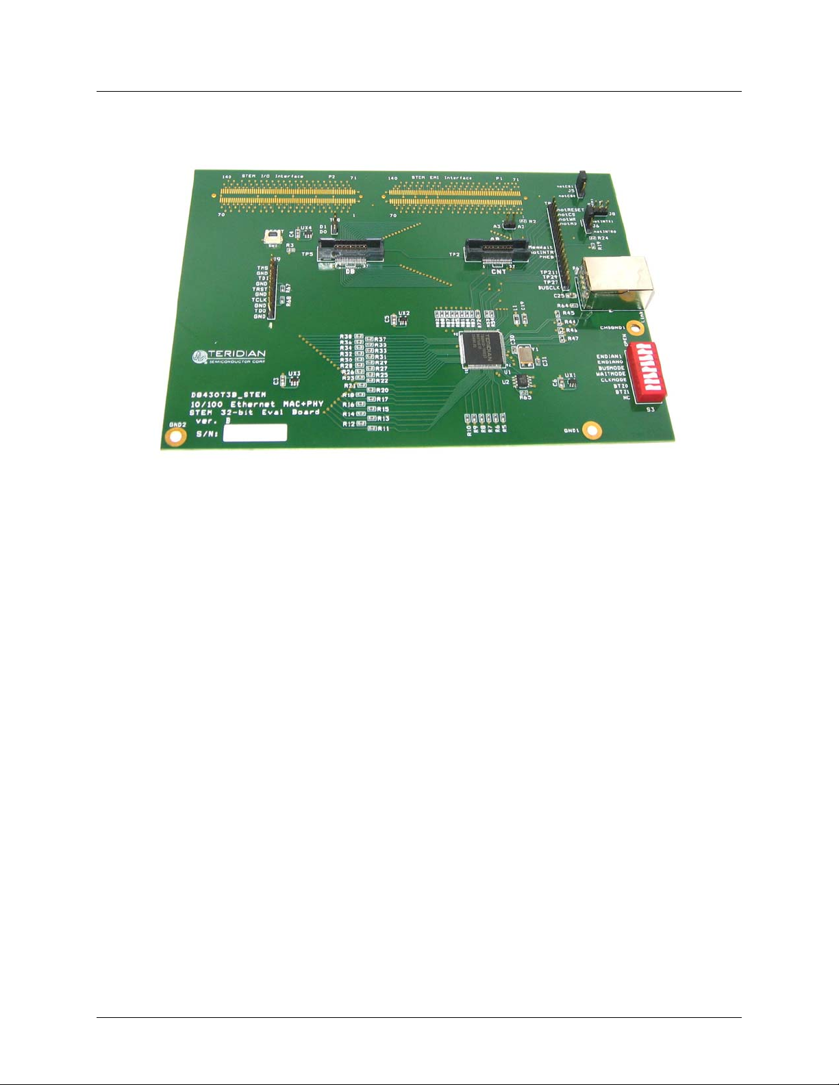
The 78Q8430 STEM Demo Board (D8430T3B_STEM) is a design example for a 10/100BASE-TX
MAC+PHY ST Microelectronics STEM daughter card. The Demo Board plugs directly into STi5100 and
STi5514 Evaluation Systems. The network connection is provided by the 78Q8430 which is a single chip
auto-sensing, auto-switching (auto-negotiation or parallel detect modes and auto-MDIX) 10/100BASE-TX
Fast Ethernet transceiver with full duplex operation capability. The device is designed specifically for the
Audio/Visual (A/V) and Set Top Box (STB) markets and is easily interfaced to available A/V and STB core
processors.
The 78Q8430 is compliant with applicable IEEE-802.3 standards. MAC and PHY configuration and
status registers are provided as specified by IEEE802.3u. The integrated MAC is supported by an
internal 32KByte transmit and receive SRAM FIFO. The partition of transmit and receive queues are
configurable through software, allowing the 78Q8430 to be tuned for specific applications. The device
contains hardware support for TCP-IP checksum and ARC address recognition.
The 78Q8430 STEM Demo Board includes support for the following 78Q8430 hardware interface
features:
The system bus interface operates like external memory with an active low chip select.
A configurable bus interface with support for little endian and big endian formats.
Supports an asynchronous 100 MHz (max) bus clock for STi5100/5514 o peration.
Supports 32-bit, 16-bit and 8 bit wide data bus formats.
Optional EEPROM interface for configuration data.
Two programmable LED outputs for PHY status.
Single +3.3V power supply voltage with common ground plane.
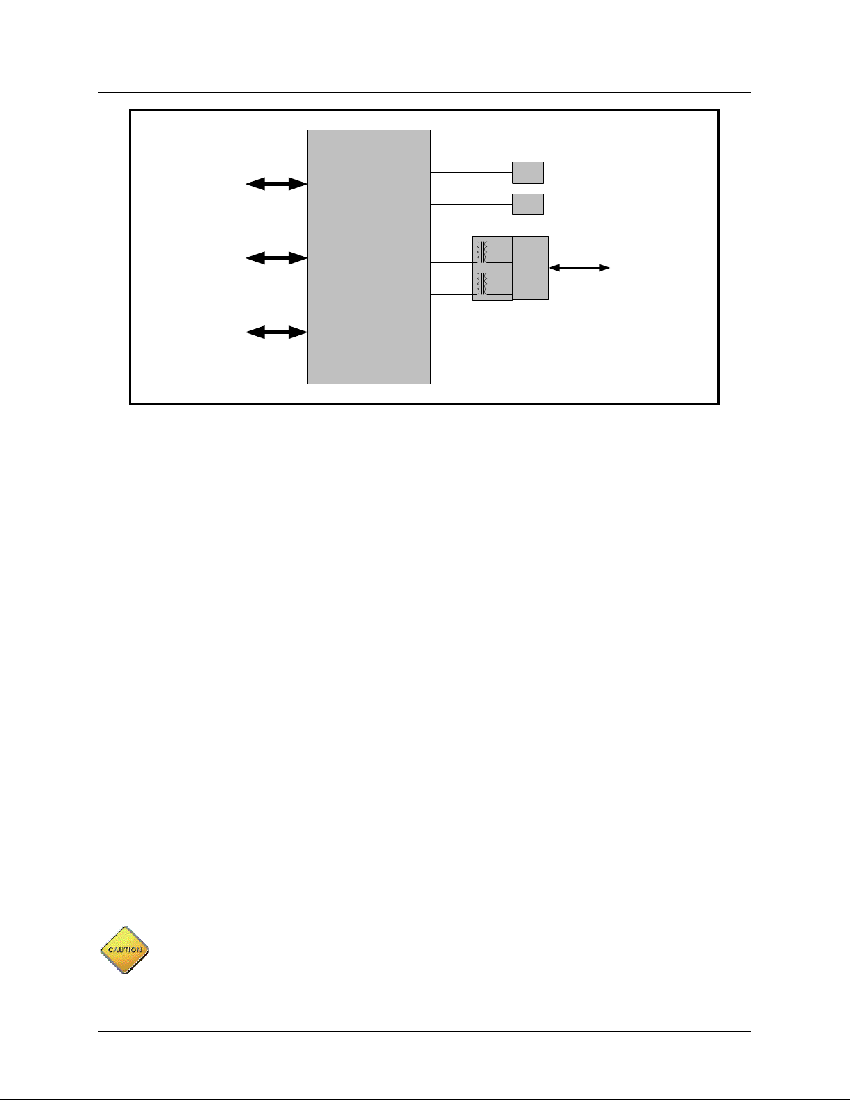
A host processor interfaces directly to the FIFO via the GBI interface. The D8430T3B_STEM board is
configured for 16-bit big endian bus format by default. The bus can optionally be configured for 32-bit or
8-bit bus widths or little endian format. Figure 1 shows the 78Q8430 system interfaces.
Rev. 1.0 5
78Q8430 STEM Demo Board User Manual UM_8430_006
32-bit/16-bit/8-bit
LED
Link (Programmable)
System
Bus
Interface
Configuration
EEPROM
Interface
78Q8430
Single C hip
10/100 Ethernet
MAC & PHY
LED
Activity (Programmable)
RJ45
CAT5
Cable
Integrated RJ-45
JTAG
Interface
with 1:1
Transformer
Figure 1: 78Q8430 System Interface Diagram
This document describes the setup and configuration of the 78Q8430 STEM Demo Board. The demo
board requires operation with a +3.3V power supply sourced from the STEM bus interface on the STi5100
evaluation board. The 78Q8430 PHY interfaces to a CAT5 UTP cable via a 1:1 transformer.
The supplied software driver includes support for ST/OS-20. The included 78Q8430 Softwar e Driver
Development Guidelines and 78Q8430 Software User Guide for ST/OS-20 describe the software
interfacing requirements for quick driver integration and prompt system evaluatio n of the 78Q8430.
Use this document with those listed in the Related Documentation section.
1.1 Package Contents
The 78Q8430 STEM Demo Board kit includes:
A 78Q8430 STEM Demo Board (D8430T3B_STEM).
A CD containing the 78Q8430 software device driver for ST/OS-20.
The following documents on CD:
78Q8430 STEM Demo Board User Manual (this document)
78Q8430 Preliminary Data Sheet
78Q8430 Layout Guidelines
78Q8430 Software Driver Development Guidelines
78Q8430 Software User Guide for ST/OS-20
The printed circuit board Gerber files are available upon request.
1.2 Safety and ESD Notes
Connecting live voltages to the demo board system will result in potentially hazardous voltages on the
boards.
The demo boards are ESD sensitive! ESD precautions must be taken when handling these
boards!
6 Rev. 1.0

UM_8430_006 78Q8430 STEM Demo Board User Manual
1.3 System Hardware Requirements
The following describes the minimum hardware requirements for the 78Q8430 Demo Board system:
The 78Q8430 STEM Demo Board (D8430T3B_STEM).
An STi5100 Evaluation Platform (available from ST).
A software development PC with the following minimum requirements: Pentium
RAM and 40 GB hard drive running either Windows
2000 or Windows XP.
4 CPU with 256 MB
An IP Video Server PC with the following minimum requirements: Pentium 4 CPU with 256 MB RAM
and 40 GB hard drive, 10/100 ports for demo board connection, running either Windows 200 0 or
Windows XP.
A 10/100Base-T hub or switch.
An ST Microconnect JTAG emulator. This device loads the IPSTB demo software into the STi5100
Evaluation Platform.
Television for viewing the video demo.
1.4 System Software Requirements
The following describes the minimum software requirements for embedded application programming
using the 78Q8430 Demo Board:
ST20 Toolset: STi5100 BSP Version 2.0.5 Patch 1 (available from ST).
IPBox: contains web_server, htdocs, and video_server folders (included in the 78Q8430 ST/OS-20
driver software release package).
IPSTB application: Ipstba3_esp – 5100 (included in the 78Q8430 ST/OS-20 driver software release
package).
Rev. 1.0 7
78Q8430 STEM Demo Board User Manual UM_8430_006
2 Hardware Setup
2.1 Jumper and Dip Switch Settings
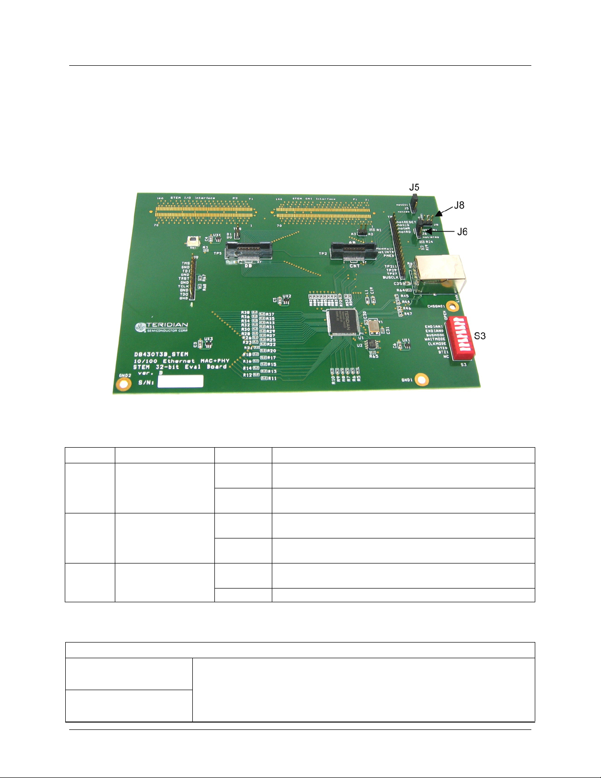
The 78Q8430 STEM Demo Board utilizes various jumpers (J5, J6, and J8) and dip switches (S3) for
establishing the startup configuration of the 78Q8430 device. Figure 2 shows the location of the jumpers
and dip switch. Table 1 and Table 2 describe the jumper and dip switch options. The jumper and switch
numbers and settings are printed on the demo board.
Figure 2: 78Q8430 STEM Demo Board Jumper and Dip Switch Locations
Table 1: Demo Board Jumper Options
Jumper Name Setting Description
J5 Chip Select Source notCS0
notCS1
J6 Interrupt Selection notINTR0
notINTR1
J8 PMEB Selection notINTR1
PMEB Connects 78Q8430 PMEB output to board PMEB signal.
Table 2: Demo Board Dip Switch Options
S3 – Device Mode Configuration Dip Switch ( 1 = open, 0 = closed)
Position 1 (ENDIAN1)
Position 2 (ENDIAN0)
Position 1, 2:
0, 0 (default) = big endian (MSB at high bit positions)
0, 1 = bytes are little endian inside 16 bit words
1, 0 = word endian (MSW at low bit positions)
1, 1 = little endian (MSB at low bit positions)
Selects STEM notCS0 for 78Q8430 chip select signal
source.
Selects STEM notCS1 for 78Q8430 chip select signal
source (default).
Connects 78Q8430 interrupt output to STEM notINTR0
signal.
Connects 78Q8430 interrupt output to STEM notINTR1
signal (default).
Connects 78Q8430 PMEB output to STEM notINTR1
signal.
8 Rev. 1.0

UM_8430_006 78Q8430 STEM Demo Board User Manual
S3 – Device Mode Configuration Dip Switch ( 1 = open, 0 = closed)
Position 3 (BUSMODE) Position 3, 5, 4:
0, 0, 0 = sync bus, external system clock, memwait act low
0, 0, 1 = sync bus, external system clock, memwait act high
Position 5 (CLCKMODE)
Position 4 (WAITMODE)
Position 6 (BTZ0) Position 6, 7:
Position 7 (BTZ1)
Position 8 (NC) No Connection
0, 1, 0 = reserved
0, 1, 1 = reserved
1, 0, 0 = async bus, external system clock, memwait act low
1, 0, 1 (default) = async bus, external system clock, memwait act high
1, 1, 0 = async bus, internal system clock, memwait act low
1, 1, 1 = async bus, internal system clock, memwait act high
0, 0 = 32 bit bus width
0, 1 (default) 16 bit bus width (only DATA[15:0] are used)
1, 0 = 8 bit bus width (only DATA [7:0] are used)
1, 1 = reserved
2.2 Connections
Connect the system components as shown in Figure 3. Refer to the STi5100 documentation for
additional information on the STi5100 Evaluation Platform connections.
Figure 3: Demo System Hardware Connections
STEP 1: Attach the 78Q8430 STEM Demo Board to the STi5100 Evaluation Board via the two 140 pin
connectors on the bottom of the demo board to the two corresponding STEM connectors on the STi5100
Evaluation Board.
Rev. 1.0 9

78Q8430 STEM Demo Board User Manual UM_8430_006
STEP 2: Connect the development PC Ethernet port to the switch/hub using a CAT-5 cable.
STEP 3: Connect the ST20 in-circuit-emulator (ICE) to the switch/hub using a CAT-5 cabl e.
STEP 4: Connect the ST20 ICE to the STi5100 Evaluation Board using the ribbon cable.
STEP 5: Connect the television to the STi5100 Evaluation Board using a video/audio cable.
STEP 6: Connect the video server PC to the STEM demo board RJ-45 connector using a CAT-5 cable.
STEP 7: Refer to the STi5100 documentation for powering up the evaluation system. The 78Q8430
STEM Demo Board receives its power through the STEM bus interface on the STi5100 Evaluation Board.
10 Rev. 1.0

UM_8430_006 78Q8430 STEM Demo Board User Manual
3 Software Setup
The path names (in italics) given in the following steps are for illustrative purposes. If the software has
been installed in different directories than those given below, replace the path in the example with the
appropriate path for your installation.
3.1 Development (Host) PC Environment Setup
The following steps describe how to set up the host PC software environment.
STEP 1: Modify the Windows Environment to use the ST20R2.0.5 tool set as follows:
Append C:\STM\ST20R2.0.5\bin; to the front
path might be C:\STM\ST20R2.0.5\bin;C:\STM\ST20R1.9.6\bin;%SystemRoot%\system32;……
STEP 2: Modify the system variable ‘ST20ROOT’ as follows:
ST20ROOT C:\STM\ST20R2.0.5
STEP 3: Reboot the PC.
3.2 Video Server PC Environment Setup
The following steps describe how to set up the MPEG2 video server PC environment.
STEP 1: Set up the ST TSVOD server for unicast video streaming:
G:\ IPBox\servers\ TS_VOD_Server
STEP 2: Set up the ST Multicast server for multicast video streaming:
G:\ IPBox\servers\ Multicast
STEP 3: Set the video server PC IP address to 192.168.1.110.
STEP 4: Start the appropriate server before requesting a video stream.
3.3 ST Microconnect Target Configuration
of the system variable ‘Path’. As an example, the new
Set the ST Microconnect Target Configuration (via Ethernet) IP addresses as follows:
Host PC: 192.168.1.100
ST Microconnect: 192.168.1.30
Video Server PC: 192.168.1.110
3.4 78Q8430 Software Device Driver
The 78Q8430 ST/OS-20 device driver software and user guide, 78Q8430 Software User Guide for
ST/OS-20, are provided with the demo board. Refer to that documentation for additional information on
configuring and installing the driver.
Rev. 1.0 11

78Q8430 STEM Demo Board User Manual UM_8430_006
4 78Q8430 STEM Demo Board Schematic, BOM and PCB Layout
.
J1/P1
VCC33
FLASHCLK
notRESET
notCS0
notCS1
notRD
notWR
A9:0
D31:0
MemWait
notINTR0
notINTR1
STEM
EMI
INTERFACE
J4/P2
J5
J6
J8
S3
U2
78Q8430B
BUSCLK
RESETB
CSB
OEB
WRB
ADDR9:0
DATA31:0
MEMWAIT
INTB
PMEB
ENDIAN0
ENDIAN1
BUSMODE
CLKMODE
WAITMODE
BOOTSZ0
BOOTSZ1
PROMCLK
PROMCS
PROMDO
PROMDI
VCCD VCCA
LED0
LED1
TXP
TXN
RXP
RXN
XTLN
XTLP
TCLK
TRST
TMS
TDO
TDI
J16
RJ45
25MHz Crystal
J9
TP2 & TP5
STEM IO Interface
Not Used
Pass Through Only
Mictor Connectors
Logic Analyzer Pods
TP1, TP4, TP8
Scope Test Points
Figure 4: STEM EMI Bus Interface Block Diagram
12 Rev. 1.0

UM_8430_006 78Q8430 STEM Demo Board User Manual
notBS notFRM
SCLK
R1
SCKEN
33
0603
GND
MemWait
notINTR0 notINTR1
FLASHCLK
notWR
notCS0
R2 33
0603
DACK2
DACK0
DRAK0
notDR0
MemWait
MemGnt
notINTR0
FCLK
notWR
notCS0 notCS1
A25
A23
A21
A19
A17
A15
A13
A11
A9
A7
A5
A3
A1
D31
D29
D27
D25
D23
D21
D19
D15
D13
D11
D9
D7
D5
D3
D1
MCLK ALE
VCC12
J1
1
notBS
2
SDRAM_CLK
3
SDRAM_CLKEN
4
MEZZ_PRESENT0
5
GROUND
6
DACK2
7
DACK0
8
DRAK0
9
notDREQ0
10
GROUND
11
MemWait
12
VCC3V3
13
MemGranted
14
notINTR0
15
GROUND
16
FLASH_CLK
17
GROUND
18
notWR
19
GROUND
20
notCS0
21
GROUND
22
A25
23
A23
24
VCC3V3
25
A21
26
A19
27
GROUND
28
A17
29
A15
30
VCC3V3
31
A13
32
A11
33
GROUND
34
A9
35
A7
36
VCC3V3
37
A5
38
A3
39
GROUND
40
A1_notBE3_DQM3
41
notBE1_DQM1
42
GROUND
43
D31
44
D29
45
GROUND
46
D27
47
D25
48
GROUND
49
D23
50
D21
51
GROUND
52
D19
53
D17
54
GROUND
55
D15
56
D13
57
GROUND
58
D11
59
D9
60
GROUND
61
D7
62
D5
63
GROUND
64
D3
65
D1
66
GROUND
67
MPX_CLK
68
GROUND
69
VCC12V
70
VCC12V
STEM EMI Connector
GND
Solder Side Connector to Motherboard
AMP 5-179010-6
STEM_J_EMI_REV1
notFRAME
notCAS
notRESET
MEZZ_PRESENT1
GROUND
DACK3
DACK1
DRAK1
notDREQ1
GROUND
AUXCLKOUT
VCC3V3
MemReq
notINTR1
GROUND
notRD_notCAS_notFRAME
GROUND
GROUND
notCS1
GROUND
VCC3V3
GROUND
VCC3V3
GROUND
VCC3V3
GROUND
A0_notBE2_DQM2
notBE0_DQM0
GROUND
GROUND
GROUND
GROUND
GROUND
ALE_notRAS_notBS
GROUND
VCC12V
VCC12V
FBAA
VCC
VCC
VCC
VCC
71
72
73
74
75
76
77
78
79
80
81
82
83
84
85
86
87
88
89
90
91
92
A24
93
A22
94
95
A20
96
A18
97
98
A16
99
A14
100
101
A12
102
A10
103
104
A8
105
A6
106
107
A4
108
A2
109
110
111
112
113
D30
114
D28
115
116
D26
117
D24
118
119
D22
120
D20
121
122
D18
123
D16
124
125
D14
126
D12
127
128
D10
129
D8
130
131
D6
132
D4
133
134
D2
135
D0
136
137
138
139
140
GND
norCAS
notRESET
MPST1MPST0
DACK3
DACK1
DRAK1
notDR1
ACLK
MemReq
notINTR1
FBAA
notRD
A24
A22
A20
A18
A16
A14
A12
A10
A8
A6
A4
A2
A0
D30
D28
D26
D24
D22
D20
D18
D16D17
D14
D12
D10
D8
D6
D4
D2
D0
notRD
notCS1
A[9:0]
D[31:0]
notBS
SCLK
notRESET
notINTR0 notINTR1
A[9:0]
D[31:0]
VCC12
SCKEN
DACK2
DACK0
DRAK0
notDR0
MemWait
MemGnt
notINTR0
FCLK
notWR
notCS0
A25
A23
A21
A19
A17
A15
A13
A11
A9
A7
A5
A3
A1
D31
D29
D27
D25
D23
D21
D19
D17
D15
D13
D11
D9
D7
D5
D3
D1
MCLK
P1
1
notBS
2
SDRAM_CLK
3
SDRAM_CLKEN
4
MEZZ_PRESENT0
5
GROUND
6
DACK2
7
DACK0
8
DRAK0
9
notDREQ0
10
GROUND
11
MemWait
12
VCC3V3
13
MemGranted
14
notINTR0
15
GROUND
16
FLASH_CLK
17
GROUND
18
notWR
19
GROUND
20
notCS0
21
GROUND
22
A25
23
A23
24
VCC3V3
25
A21
26
A19
27
GROUND
28
A17
29
A15
30
VCC3V3
31
A13
32
A11
33
GROUND
34
A9
35
A7
36
VCC3V3
37
A5
38
A3
39
GROUND
40
A1_notBE3_DQM3
41
notBE1_DQM1
42
GROUND
43
D31
44
D29
45
GROUND
46
D27
47
D25
48
GROUND
49
D23
50
D21
51
GROUND
52
D19
53
D17
54
GROUND
55
D15
56
D13
57
GROUND
58
D11
59
D9
60
GROUND
61
D7
62
D5
63
GROUND
64
D3
65
D1
66
GROUND
67
MPX_CLK
68
GROUND
69
VCC12V
70
VCC12V
STEM EMI Connector
GND
Component Side Expansion Connector
Pass Through
AMP 179031-6
STEM_P_EMI
notFRAME
notCAS
notRESET
MEZZ_PRESENT1
GROUND
DACK3
DACK1
DRAK1
notDREQ1
GROUND
AUXCLKOUT
VCC3V3
MemReq
notINTR1
GROUND
notRD_notCAS_notFRAME
GROUND
GROUND
notCS1
GROUND
VCC3V3
GROUND
VCC3V3
GROUND
VCC3V3
GROUND
A0_notBE2_DQM2
notBE0_DQM0
GROUND
GROUND
GROUND
GROUND
GROUND
ALE_notRAS_notBS
GROUND
VCC12V
VCC12V
FBAA
VCC
VCC
VCC
VCC
GND
notFRM
norCAS
notRESET
DACK3
DACK1
DRAK1
notDR1
ACLK
MemReq
notINTR1
FBAA
notRD
notCS1
A24
A22
A20
A18
A16
A14
A12
A10
A8
A6
A4
A2
A0
D30
D28
D26
D24
D22
D20
D18
D16
D14
D12
D10
D8
D6
D4
D2
D0
ALE
71
72
73
74
75
76
77
78
79
80
81
82
83
84
85
86
87
88
89
90
91
92
A24
93
A22
94
95
A20
96
A18
97
98
A16
99
A14
100
101
A12
102
A10
103
104
A8
105
A6
106
107
A4
108
A2
109
110
111
112
113
D30
114
D28
115
116
D26
117
D24
118
119
D22
120
D20
121
122
D18
123
D16
124
125
D14
126
D12
127
128
D10
129
D8
130
131
D6
132
D4
133
134
D2
135
D0
136
137
138
139
140
C3
10
0805
C4
10
0805
VCC5
GND
C5
10
0805
GND
C6
10
0805
GND
VCC5
+3.3V
GND1
1
GND
1
MTHOLE
GND2
1
GND
1
MTHOLE
Figure 5: STEM EMI Bus Interface Schematic
Rev. 1.0 13

78Q8430 STEM Demo Board User Manual UM_8430_006
VCC5
STEMIO4
STEMIO5
STEMIO7
STEMIO8
STEMIO10
STEMIO13
STEMIO14
STEMIO16
STEMIO17
STEMIO19
STEMIO22
STEMIO23
STEMIO25
STEMIO26
STEMIO28
STEMIO29
STEMIO31
STEMIO32
STEMIO34
STEMIO35
STEMIO37
STEMIO38
STEMIO40
STEMIO43
STEMIO44
STEMIO46
STEMIO47
STEMIO49
STEMIO52
STEMIO53
STEMIO55
STEMIO56
STEMIO58
STEMIO60
STEMIO62
STEMIO64
STEMIO65
STEMIO67
STEMIO69
VCC5
J4
1
VCC12V
2
VCC12V
3
GROUND
4
TS_OUT_DATA7
5
TS_OUT_DATA5
6
GROUND
7
TS_OUT_DATA3
8
TS_OUT_DATA1
9
GROUND
10
TS_OUT_CLK
11
GROUND
12
VCC
13
TS_IN0_DATA7
14
TS_IN0_DATA5
15
GROUND
16
TS_IN0_DATA3
17
TS_IN0_DATA1
18
GROUND
19
TS_IN0_CLK
20
GROUND
21
VCC
22
AVData7
23
AVData5
24
GROUND
25
AVData3
26
AVData1
27
GROUND
28
AVPacketErr
29
AVByteClk
30
GROUND
31
AVPacketTag0
32
AVPacketTag2
33
VCC
34
TS_IN1_DATA7
35
TS_IN1_DATA5
36
GROUND
37
TS_IN1_DATA3
38
TS_IN1_DATA1
39
GROUND
40
TS_IN1_CLK
41
GROUND
42
VCC
43
TS_IN2_DATA7
44
TS_IN2_DATA5
45
GROUND
46
TS_IN2_DATA3
47
TS_IN2_DATA1
48
GROUND
49
TS_IN2_CLK
50
GROUND
51
VCC
52
YUV7
53
YUV5
54
GROUND
55
YUV3
56
YUV1
57
GROUND
58
VSYNC
59
GROUND
60
PIXCLK
61
GROUND
62
SCLK
63
GROUND
64
PCM3
65
PCM1
66
GROUND
67
I2C_CLK
68
GROUND
69
Reserved
70
VCC
STEM IO Connector
GND GND
AMP 5-179010-6
TS_OUT_DATA6
TS_OUT_DATA4
TS_OUT_DATA2
TS_OUT_DATA0
TS_OUT_DSTRT
TS_OUT_DVAL
TS_IN0_DATA6
TS_IN0_DATA4
TS_IN0_DATA2
TS_IN0_DATA0
TS_IN0_DSTRT
TS_IN0_DVAL
AVPacketClk
AVByteClkValid
AVPacketTag1
AVPacketTag3
TS_IN1_DATA6
TS_IN1_DATA4
TS_IN1_DATA2
TS_IN1_DATA0
TS_IN1_DSTRT
TS_IN1_DVAL
TS_IN2_DATA6
TS_IN2_DATA4
TS_IN2_DATA2
TS_IN2_DATA0
TS_IN2_DSTRT
TS_IN2_DVAL
VCC12V
VCC12V
GROUND
GROUND
GROUND
GROUND
GROUND
GROUND
GROUND
AVData6
AVData4
GROUND
AVData2
AVData0
GROUND
GROUND
VCC
GROUND
GROUND
GROUND
GROUND
GROUND
GROUND
YUV6
YUV4
GROUND
YUV2
YUV0
GROUND
HSYNC
GROUND
MCLK
GROUND
LRCLK
GROUND
PCM2
PCM0
GROUND
I2C_SDA
GROUND
notRESET
VCC
71
72
73
74
75
76
77
78
79
80
81
82
83
84
85
86
87
88
89
90
91
92
93
94
95
96
97
98
99
100
101
102
103
104
105
106
107
108
109
110
111
112
113
114
115
116
117
118
119
120
121
122
123
124
125
126
127
128
129
130
131
132
133
134
135
136
137
138
139
140
GND
STEMIO74
STEMIO75
STEMIO77
STEMIO78
STEMIO80
STEMIO81
STEMIO83
STEMIO84
STEMIO86
STEMIO87
STEMIO89
STEMIO90
STEMIO92
STEMIO93
STEMIO95
STEMIO96
STEMIO98
STEMIO99
STEMIO101
STEMIO102
STEMIO104
STEMIO105
STEMIO107
STEMIO108
STEMIO110
STEMIO111
STEMIO113
STEMIO114
STEMIO116
STEMIO117
STEMIO119
STEMIO120
STEMIO122
STEMIO123
STEMIO125
STEMIO126
STEMIO128
STEMIO130
STEMIO132
STEMIO134
STEMIO136
STEMIO138
STEMIO140
STEMIO4
STEMIO5
STEMIO7
STEMIO8
STEMIO10
STEMIO13
STEMIO14
STEMIO16
STEMIO19
STEMIO22
STEMIO23
STEMIO25
STEMIO26
STEMIO28
STEMIO29
STEMIO31
STEMIO34
STEMIO35
STEMIO37
STEMIO38
STEMIO40
STEMIO43
STEMIO44
STEMIO46
STEMIO47
STEMIO49
STEMIO52
STEMIO53
STEMIO55
STEMIO56
STEMIO58
STEMIO60
STEMIO62
STEMIO64
STEMIO65
STEMIO67
STEMIO69
P2
1
VCC12V
2
VCC12V
3
GROUND
4
TS_OUT_DATA7
5
TS_OUT_DATA5
6
GROUND
7
TS_OUT_DATA3
8
TS_OUT_DATA1
9
GROUND
10
TS_OUT_CLK
11
GROUND
12
VCC
13
TS_IN0_DATA7
14
TS_IN0_DATA5
15
GROUND
16
TS_IN0_DATA3
17
TS_IN0_DATA1
18
GROUND
19
TS_IN0_CLK
20
GROUND
21
VCC
22
AVData7
23
AVData5
24
GROUND
25
AVData3
26
AVData1
27
GROUND
28
AVPacketErr
29
AVByteClk
30
GROUND
31
AVPacketTag0
32
AVPacketTag2
33
VCC
34
TS_IN1_DATA7
35
TS_IN1_DATA5
36
GROUND
37
TS_IN1_DATA3
38
TS_IN1_DATA1
39
GROUND
40
TS_IN1_CLK
41
GROUND
42
VCC
43
TS_IN2_DATA7
44
TS_IN2_DATA5
45
GROUND
46
TS_IN2_DATA3
47
TS_IN2_DATA1
48
GROUND
49
TS_IN2_CLK
50
GROUND
51
VCC
52
YUV7
53
YUV5
54
GROUND
55
YUV3
56
YUV1
57
GROUND
58
VSYNC
59
GROUND
60
PIXCLK
61
GROUND
62
SCLK
63
GROUND
64
PCM3
65
PCM1
66
GROUND
67
I2C_CLK
68
GROUND
69
Reserved
70
VCC
STEM IO Connector
Component Side Expansion ConnectorSolder Side Connector to Motherboard
Pass Through
AMP 179031-6STEM_J_IO_REV1
STEM_P_IO
VCC12V
VCC12V
GROUND
TS_OUT_DATA6
TS_OUT_DATA4
GROUND
TS_OUT_DATA2
TS_OUT_DATA0
GROUND
TS_OUT_DSTRT
TS_OUT_DVAL
GROUND
TS_IN0_DATA6
TS_IN0_DATA4
GROUND
TS_IN0_DATA2
TS_IN0_DATA0
GROUND
TS_IN0_DSTRT
TS_IN0_DVAL
GROUND
AVData6
AVData4
GROUND
AVData2
AVData0
GROUND
AVPacketClk
AVByteClkValid
GROUND
AVPacketTag1
AVPacketTag3
VCC
TS_IN1_DATA6
TS_IN1_DATA4
GROUND
TS_IN1_DATA2
TS_IN1_DATA0
GROUND
TS_IN1_DSTRT
TS_IN1_DVAL
GROUND
TS_IN2_DATA6
TS_IN2_DATA4
GROUND
TS_IN2_DATA2
TS_IN2_DATA0
GROUND
TS_IN2_DSTRT
TS_IN2_DVAL
GROUND
YUV6
YUV4
GROUND
YUV2
YUV0
GROUND
HSYNC
GROUND
MCLK
GROUND
LRCLK
GROUND
PCM2
PCM0
GROUND
I2C_SDA
GROUND
notRESET
VCC
71
72
73
74
75
76
77
78
79
80
81
82
83
84
85
86
87
88
89
90
91
92
93
94
95
96
97
98
99
100
101
102
103
104
105
106
107
108
109
110
111
112
113
114
115
116
117
118
119
120
121
122
123
124
125
126
127
128
129
130
131
132
133
134
135
136
137
138
139
140
GND
STEMIO74
STEMIO75
STEMIO77
STEMIO78
STEMIO80
STEMIO81
STEMIO83
STEMIO84
STEMIO86
STEMIO87STEMIO17
STEMIO89
STEMIO90
STEMIO92
STEMIO93
STEMIO95
STEMIO96
STEMIO98
STEMIO99
STEMIO101
STEMIO102STEMIO32
STEMIO104
STEMIO105
STEMIO107
STEMIO108
STEMIO110
STEMIO111
STEMIO113
STEMIO114
STEMIO116
STEMIO117
STEMIO119
STEMIO120
STEMIO122
STEMIO123
STEMIO125
STEMIO126
STEMIO128
STEMIO130
STEMIO132
STEMIO134
STEMIO136
STEMIO138
STEMIO140
VCC12
VCC12
Figure 6: STEM IO Bus Interface Schematic
14 Rev. 1.0

UM_8430_006 78Q8430 STEM Demo Board User Manual
TP1
FLASHCLK
PMEB
notINTR
MemWait
notRD
notWR
notCS
notRESET
112233445566778899101011111212131314141515161617
17
FLASHCLK
TP27
TP29
TP211
PMEB
notINTR
MemWait
notRD
notWR
notCS
notRESET
(MSB)
D31
D30
D29
D28
D27
D26
D25
D24
D22
D21
D20
D19
D18
D17
D16
GND
TP2
1
NC
3
GND
5
CLKE
7
D15E
9
D14E
11
D13E
13
D12E
15
D11E
17
D10E
19
D9E
21
D8E
23
D7E
25
D6E
27
D5E
29
D4E
31
D3E
33
D2E
35
D1E
37
D0E
GND39GND40GND41GND42GND
GND
TP5
1
NC
3
GND
5
CLKE
7
D15E
9
D14E
11
D13E
13
D12E
15
D11E
17
D10E
19
D9E
21
D8E
23
D7E
25
D6E
27
D5E
29
D4E
31
D3E
33
D2E
35
D1E
37
D0E
GND39GND40GND41GND42GND
GND
CLKO
D15O
D14O
D13O
D12O
D11O
D10O
D9O
D8O
D7O
D6O
D5O
D4O
D3O
D2O
D1O
D0O
CLKO
D15O
D14O
D13O
D12O
D11O
D10O
D9O
D8O
D7O
D6O
D5O
D4O
D3O
D2O
D1O
D0O
2
NC
4
NC
6
8
10
12
14
16
18
20
22
24
26
28
30
32
34
36
38
43
2
NC
4
NC
6
8
10
12
14
16
18
20
22
24
26
28
30
32
34
36
38
43
A9
A8
A7
A6
A5
A4
A3
A2
A1
A0
Mictor 38 Pin Connector
AMP
2-767004-2
D15
D14
D13
D12
D11
D10
D9
D8
D7D23
D6
D5
D4
D3
D2
D1
D0
Mictor 38 Pin Connector
AMP
2-767004-2
(MSB)
(LSB)
(LSB)
A[9:0]
A3
A2
D1
D0
TP4
1
2
A[9:0]
1
2
TP8
1
1
2
2
D[31:0]
D[31:0]
Figure 7: MICTOR Diagnostic Connectors Schematic
Rev. 1.0 15

78Q8430 STEM Demo Board User Manual UM_8430_006
.
FLASHCLK
R3
notRESET
R95
10K
0603
notRESET
100
0603
notCS
notCS0 notRD
notCS1
+3.3V
R93
R94
10K
10K
0603
0603
R92
10K
0603
J5
1
1
2
2
3
3
R89
R90
R91
10K
10K
10K
0603
0603
0603
SW1
RESET
EVQPJU
ENDIAN1
ENDIAN0
BUSMODE
WAITMODE
CLKMODE
BTZ0
BTZ1
notWR
A[9:0]
1
2
3
4
5
6
7
8
GND
+3.3V
61
82
FLASHCLK
RSTB
notCS
notWR
A[9:0]
S3
16
15
14
13
12
11
10
9
notRD
A9
A8
A7
A6
A5
A4
A3
A2
A1
A0
ENDIAN1
ENDIAN0
BUSMODE
WAITMODE
CLKMODE
BTZ1
BTZ0
PROMCLK
PROMCS
PROMDO
PROMDI
R82 33
R88 33
R87 33
R86 33
R85 33
R81 33
R84 33
R83 33
R54 33
R53 33
TDI
TDO
TMS
TRST
TCLK
+3.3V
2
1
3
CLK
CS
DI
(MSB)
(LSB)
8
93LC46B
5
15
BUSCLK
7
RESETB
16
CSB
11
WRB
12
OEB
25
ADDR9
24
ADDR8
23
ADDR7
22
ADDR6
21
ADDR5
20
ADDR4
19
ADDR3
18
ADDR2
9
ADDR1
10
ADDR0
80
ENDIAN1
79
ENDIAN0
83
BUSMODE
84
WAITMODE
85
CLKMODE
100
BOOTSZ1
1
BOOTSZ0
74
PROMCLK
75
PROMCS
76
PROMDO
77
PROMDI
4
TDI
81
TDO
3
TMS
5
TRST
6
TCLK
U1A
78Q8430B-100
U2
DO
VCC
NC1
NC2
GND
Not Installed
+3.3V
2 4
4
7
6
53
VCC18VCC217VCC336VCC427VCC537VCC644VCC751VCC871VCC9
GND12GND214GND334GND435GND526GND643GND750GND860GND970GND11
GND
R65
10K
0603
GND
UX1
Spare
SOT23_5
78
53
2 4
GNDGND
VCC11
MEMWAIT
UX2
Spare
SOT23_5
GND
GND
DATA31
DATA30
DATA29
DATA28
DATA27
DATA26
DATA25
DATA24
DATA23
DATA22
DATA21
DATA20
DATA19
DATA18
DATA17
DATA16
DATA15
DATA14
DATA13
DATA12
DATA11
DATA10
DATA9
DATA8
DATA7
DATA6
DATA5
DATA4
DATA3
DATA2
DATA1
DATA0
INTB
PMEB
C9
0.1
0603
C14
0.1
0603
13
69
68
67
66
65
64
63
62
59
58
57
56
55
54
53
52
49
48
47
46
45
42
41
40
39
38
33
32
31
30
29
28
72
73
2 4
C11
C10
0.1
0603
GND GNDGND GND
C15
0.1
0603
GND GNDGND
DB31
DB30
DB29
DB28
DB27
DB26
DB25
DB24
DB23
DB22
DB21
DB20
DB19
DB18
DB17
DB16
DB15
DB14
DB13
DB12
DB11
DB10
DB9
DB8
DB7
DB6
DB5
DB4
DB3
DB2
DB1
DB0
53
UX3
Spare
SOT23_5
C12
0.1
0.1
0603
0603
C17
C16
0.1
0.1
0603
0603
R72
10K
0603
R5 33 0603
R7 33 0603
R9 33 0603
R11 33 0603
R13 33 0603
R15 33 0603
R17 33 0603
R20 33 0603
R22 33 0603
R25 33 0603
R27 33 0603
R29 33 0603
R31 33 0603
R33 33 0603
R35 33 0603
R37 33 0603
notINTR
PMEB
R67
10K
0603
2 4
GND
R6 33 0603
R8 33 0603
R10 33 0603
R12 33 0603
R14 33 0603
R16 33 0603
R18 33 0603
R21 33 0603
R23 33 0603
R26 33 0603
R28 33 0603
R30 33 0603
R32 33 0603
R34 33 0603
R36 33 0603
R38 33 0603
R68
10K
0603
GND
53
GNDGND
C13
0.1
0603
C18
0.1
0603
UX4
Spare
SOT23_5
TMS
TDI
TRST
TCLK
TDO
+3.3V
R71
10K
0603
(MSB)
(LSB)
D31
D30
D29
D28
D27
D26
D25
D24
D23
D22
D21
D20
D19
D18
D17
D16
D15
D14
D13
D12
D11
D10
D9
D8
D7
D6
D5
D4
D3
D2
D1
D0
J9
1
2
3
4
5
6
7
8
9
10
CON10
+3.3V
R19
10K
0603
+3.3V
D[31:0]
R69
10K
0603
R4
33
0603
R24
33
0603
R70
33
0603
MEMWAITMEMWT
notINTR0
J62
J82
1
2
3
notINTR1
1
2
3
MemWait
D[31:0]
notINTR0
J6
1
2
3
notINTR1
notINTR
J8
1
2
3
PMEB
Figure 8: 78Q8430 MAC Interface Schematic
16 Rev. 1.0

UM_8430_006 78Q8430 STEM Demo Board User Manual
+3.3V
R63
680
0603
J16
9
10
1
2
3
4
5
6
7
8
11
12
J0011F01P TabUp
Pulse Engr
CGND
R64
680
0603
+3.3V
RALED
RCLED
LCLED
LALED
CGND3
TD+
TDTDCT
CGND1
CGND2
RDCT
RD+
RD-
CGND4
RX/TX
Link
13 14
CHSGND1
CGND
+3.3V
L1
FERRITE
R_0805
Use Zero Ohm Resistor
VCCA
C19
10
0805
U1B
78Q8430B-100
GND
96
VCCA186VCCA295VCCA3
GNDA189GNDA291GNDA3
99
LED1
LED0
TXN
RXP
RXN
XTLP
XTLN
TXP
C20
0.1
0603
C21
0.1
0603
GNDGND
LED1
92
LED0
90
TXOP
97
TXON
98
RXIP
94
RXIN
93
XTLP
87
XTLN
88
C30
27PF
0603
C22
0.1
0603
GND
Gnd pins 2 and 4
Y1
1 3
25.000MHZ
50ppm
Raltron
GND GND
L11B
C31
27PF
0603
GND
C23
0.1
0603
R44
49.9
1%
0603
R45
49.9
1%
0603
R46
49.9
1%
0603
R47
49.9
1%
0603
Link
GND
Activity
C24
0.1
0603
C25
10
0805
GNDGND
Figure 9: 78Q8430 PHY Interface Schematic
1
CGND
Rev. 1.0 17

78Q8430 STEM Demo Board User Manual UM_8430_006
Table 3: STEM Demo Board Bill of Materials
Item Quantity Reference Part
PCB
Footprint
Part
Number
Vendor
1 2 C30,C31 CAP, 27pF, 50V C_0603 C1608C0G1H270J TDK
2 15 C9-C18,C20-C24 CAP, 0.1uF, 16V C_0603 ECJ-1VB1E104K Panasonic
3 6 C3-C6,C19,C25 CAP,10uF,10V C_0805
GRM21BR61A106K
E19L
Murata
4 0 GND1,GND2 MTHOLE MTHOLE
Sullins
5 3 J5,J6,J8 CON3 SIP\3P PBC03SAAN
Electronics
Corp
Sullins
6 2 TP4,TP8 CON2 SIP\2P PBC02SAAN
Electronics
Corp
Sullins
7 1 J9 CON10 SIP\10P PBC10SAAN
Electronics
Corp
8 2 J1,J4 STEM connector STEM CON 5-5179010-6 AMP
9 1 J16 Integrated RJ45 RJ45-INT J1011F01P Pulse Eng
10 1 Y1 25MHz Crystal XTAL-SMD ABMM-25MHz Abracon
11 1 L1 (USE 0-oh m) Ferrite Bead L_0805 MMZ2012S181A TDK
12 14
R19,R65,R67-R69,
R71,R72,R89-R95
RES, 10k, 5% R_0603 ERJ-3GEYJ103V Panasonic
13 1 SW1 Switch, PB PB EVQ-PJX05M Panasonic
14 1 S3
8-Position DIP
Switch
DIPSW-16 90HBJ08PT Grayhill, Inc
15 4 R44-R47 RES, 49.9, 1% R_0603 ERJ-3EKF49R9V Panasonic
R1,R2,R4-R18,
16 47
R20-R38, R53,
RES, 33, 5% R_0603 ERJ-3GEYJ330V Panasonic
R54,R70,R81-R88
17 1 R3 RES,100,5% R_0603 ERJ-3GEYJ101V Panasonic
18 2 R63, R64 RES, 680, 5% R_0603 ERJ-3GEYJ681V Panasonic
Sullins
19 1 TP1 CON17 SIP\17P PBC17SAAN
Electronics
Corp
20 2 TP2,TP5 Mictor 38-pin MICTOR 2-767004-2 Tyco
21 1 U1 78Q8430 100 LQFP 78Q8430
Teridian
Semiconductor
22 1 U2 93LC46 SOIC8 93LC46BT-I/SN Microchip
23 4 UX1-UX4
Spare – not
installed
18 Rev. 1.0

UM_8430_006 78Q8430 STEM Demo Board User Manual
Figure 10: Top Silkscreen Layout
Figure 11: Top Layer Layout
Rev. 1.0 19

78Q8430 STEM Demo Board User Manual UM_8430_006
Figure 12: Ground Layer Layout
Figure 13: Inner Layer 1 Layout
20 Rev. 1.0

UM_8430_006 78Q8430 STEM Demo Board User Manual
Figure 14: Inner Layer 2 Layout
Figure 15: VCC Layer Layout
Rev. 1.0 21

78Q8430 STEM Demo Board User Manual UM_8430_006
Figure 16: Bottom Layer Layout
Figure 17: Bottom Silkscreen Layout
22 Rev. 1.0

UM_8430_006 78Q8430 STEM Demo Board User Manual
5 Ordering Information
Table 4 lists the order number and description for the 78Q8430 STEM Demo Board.
Table 4: Order Numbers and Description
Part Description Order Number
78Q8430 STEM Demo Board (D8430T3B_STEM) 78Q8430STEM-DB
6 Related Documentation
The following 78Q8430 documents are available from Teridian Semiconducto r Corporation:
78Q8430 Preliminary Data Sheet
78Q8430 Layout Guidelines
78Q8430 Software Driver Development Guidelines
78Q8430 Software User Guide for ST/OS-20
78Q8430 STEM Demo Board User Manual
78Q8430 ARM9 Linux Driver User and Test Guide
78Q8430 Embest Evaluation Board User Manual
7 Contact Information
For more information about Teridian Semiconductor products or to check the availability of the 78Q8430,
contact us at:
6440 Oak Canyon Road
Suite 100
Irvine, CA 92618-5201
Telephone: (714) 508-8800
FAX: (714) 508-8878
Email: lan.support@teridian.com
For a complete list of worldwide sales offices, go to http://www.teridian.com.
Rev. 1.0 23

78Q8430 STEM Demo Board User Manual UM_8430_006
Revision History
Revision Date Description
1.0 03/20/2008 First publication.
24 Rev. 1.0
 Loading...