

TERIDIAN Semiconductor 78Q8430 User Manual

78Q8430 10/100 Ethernet
MAC and PHY
Simplifying System Integration
TM
DATA SHEET
March 2009
DESCRIPTION
The Teridian 78Q8430 is a 10/100 Fast Ethernet
controller supporting multi-media offload . The
device is optimized for host processor off l oadi ng
and throughput enhancements for demanding
multi-media applications found in Set Top Box,
IP Video and Broadband Media Appliance
applications. The 78Q8430 seamlessly
interfaces to non-PCI processors through a
simplified pseudo SRAM-like Host Bus Interface
supporting 32/16/8 bit data bus widths.
Supported features include IEEE802.3x flow
control and full IEEE802.3 and 802.3u standard s
compliance.
Supporting 10Base-T and 100Base-TX, the
transceiver provides Auto MDI-X cable
cross-over correction, AUTO Negotiation, Link
Configuration and full/half duplex support with
full duplex flow control. The line interface
requires only a dual 1:1 isolation transfor m er.
Numerous packet processing and IP address
resolution control functions are incorporated,
including an extensive set of Error Monitoring,
Reporting and Troubleshooting features. The
78Q8430 provides optimal 10/100 Ethernet
connectivity in demanding video streaming and
mixed-media applications.
BENEFITS
• Support for IEEE-802.3, IEEE-802.3u and
IEEE-802.3-2000 Annex 31.B
• Low host CPU utilization/overhead with
minimal software driver overhead and small
driver memory space requirements
• Improved packet processing, low latency and
low host CPU utilization
• Highest performance streaming Video over IP
• Optimized performance in mixed media
application such as video, data and voice
• Ease of use, faster development cycles, high
throughput
• Optimized power conservation with automatic
turn on when needed
• Reduced host CPU utilization and overhead
• Improved packet processing
• Optimized performance in mixed media
applications
FEATURES
• Single chip 10Base-T/100Base-TX
IEEE-802.3 compliant MAC and PHY
Adaptive 32 kB SRAM FIFO memory
allocation between Tx and Rx paths
Queue independent user settable water
marks
Per queue status indication
• Address Resolution Controller (ARC)
Multiple perfect address filtering: 8 default
(max 12)
Wildcard address filtering, individual,
multicast and broadcast address
recognition and filtering
Positive/negative filtering and promiscuous
mode
• 64 kB JUMBO packet support
• QoS: 4 Transmit priority levels
• Non-PCI pseudo-SRAM Host Bus Interface
8-bit, 16-bit and 32-bit bus width
Big/little endian support for 16-bit/32-bit bus
widths
Asynchronous (100 MHz) and synchronous
(50 MHz) bus clock support
• Low power and flexible power supply
management
Power down/save
Wake on LAN (Magic Packet™, OnNow
packet)
Link status change
• Traffic Offload Engine Functionality
Transfer frame: APF & ICMP Echo
IP Firewall configuration: drop frames on
source IP address
IP Checksum
• Available in an industrial temperature range
-40 °C to +85 °C)
(
• RoHS compliant (6/6) lead-free package
APPLICATIONS
• Satellite, cabl e and IPTV Set Top Boxes
• Multi Media Residential Gateways
• High Definition 1080p/1080i DTVs
• IP-PVR and video distribution systems
• Digital Video Recorders/Pl ay ers
• Routers and IADs
• Video over IP system, IP-PBX
• IP Security Cameras / PVRs
• Low latency industrial automation
Rev. 1.2 © 2009 Teridian Semiconductor Corporation 1

78Q8430 Data Sheet DS_8430_001
Table of Contents
1 Introduction ......................................................................................................................................... 7
1.1
Systems Applications ................................................................................................................... 7
System Level Application Information .......................................................................................... 8
1.2
Set Top Box Application .................................................................................................. 8
1.2.1
IP Security Application ..................................................................................................... 8
1.2.2
IP PBX Application ........................................................................................................... 9
1.2.3
Overview ...................................................................................................................................... 9
1.3
Application Environments .......................................................................................................... 10
1.4
Supply Voltages ......................................................................................................................... 10
1.5
Power Management ................................................................................................................... 10
1.6
Pinout ................................................................................................................................................. 11
2
Pin Description .................................................................................................................................. 12
3
3.1
Pin Legend ................................................................................................................................. 12
Pin Descriptions ......................................................................................................................... 12
3.2
Clock Pins ...................................................................................................................... 12
3.2.1
Media Dependent Interface (MDI) Pins ......................................................................... 13
3.2.2
LED Display (PHY) Pins ................................................................................................ 13
3.2.3
EEPROM Pins ............................................................................................................... 13
3.2.4
GBI Data Pins ................................................................................................................ 14
3.2.5
3.2.6 GBI Address Pins .......................................................................................................... 15
GBI Control Pins ............................................................................................................ 15
3.2.7
Mode Pins ...................................................................................................................... 16
3.2.8
JTAG Pins ...................................................................................................................... 16
3.2.9
Power Pins ..................................................................................................................... 17
3.2.10
Electrical Specification ..................................................................................................................... 18
4
4.1
Absolute Maximum Ratings ....................................................................................................... 18
Recommended Operation Conditions ........................................................................................ 18
4.2
DC Characteristics ..................................................................................................................... 18
4.3
Digital I/O Characteristics .......................................................................................................... 19
4.4
Analog Electrical Characteristics ............................................................................................... 19
4.5
100Base-TX Transmitter ................................................................................................ 19
4.5.1
100Base-TX Transmitter (Informative) .......................................................................... 19
4.5.2
100Base-TX Receiver .................................................................................................... 20
4.5.3
10Base-T Transmitter .................................................................................................... 20
4.5.4
10Base-T Transmitter (Informative) ............................................................................... 20
4.5.5
10Base-T Receiver ........................................................................................................ 21
4.5.6
Host Interface Timing Specification ................................................................................................ 22
5
5.1
Host Interface ............................................................................................................................. 22
5.1.1 Synchronous Mode Timing ............................................................................................ 23
Bus Clock Timing ........................................................................................................... 24
5.1.2
Reset Timing .................................................................................................................. 24
5.1.3
Functional Description ..................................................................................................................... 25
6
6.1
Internal Block Diagrams ............................................................................................................. 25
Internal Digital Block ...................................................................................................... 25
6.1.1
Internal PHY ................................................................................................................... 25
6.1.2
Data Queuing ............................................................................................................................. 26
6.2
Host Interface ............................................................................................................................. 27
6.3
Reading Receive Data ................................................................................................... 27
6.3.1
Writing Transmit Data .................................................................................................... 27
6.3.2
DMA Slave Mode Access .............................................................................................. 29
6.3.3
Snoop Mode Access .................................................................................................................. 29
6.4
Water Marking ............................................................................................................................ 30
6.5
Interrupt Watermark ....................................................................................................... 30
6.5.1
2 Teridian Proprietary and Confidential Rev. 1.2

DS_8430_001 78Q8430 Data Sheet
6.5.2 PAUSE Watermark ........................................................................................................ 30
Headroom Watermark ................................................................................................... 30
6.5.3
Counters ..................................................................................................................................... 30
6.6
Summary of Counters .................................................................................................... 30
6.6.1
Reading and Setting Counter Values ............................................................................ 31
6.6.2
Precision Counting ......................................................................................................... 32
6.6.3
Rollover Interrupts ......................................................................................................... 32
6.6.4
Packet Classification .................................................................................................................. 32
6.7
Address Filtering ............................................................................................................ 34
6.7.1
Configuring the CAM ..................................................................................................... 38
6.7.2
Frame Format ................................................................................................................ 39
6.7.3
Default CAM Rule Summary .......................................................................................... 39
6.7.4
Timers ........................................................................................................................................ 44
6.8
PAUSE Timer ................................................................................................................. 44
6.8.1
HNR Timer ..................................................................................................................... 44
6.8.2
Interrupt Delay Timer ..................................................................................................... 44
6.8.3
EEPROM Controller ................................................................................................................... 44
6.9
Ethernet MAC ............................................................................................................................ 44
6.10
MAC Transmit Block ...................................................................................................... 44
6.10.1
MAC Receive Block ....................................................................................................... 45
6.10.2
MAC Control Register .................................................................................................... 45
6.10.3
Transmitting a Frame ..................................................................................................... 45
6.10.4
IEEE 802.3 Transmit Protocols ...................................................................................... 45
6.10.5
Transmit Operation ........................................................................................................ 46
6.10.6
Receiving a Frame ......................................................................................................... 46
6.10.7
Strip Padding/FCS ......................................................................................................... 47
6.10.8
MAC Error Reporting ................................................................................................................. 47
6.11
MAC Transmit Errors ..................................................................................................... 47
6.11.1
MAC Receive Errors ...................................................................................................... 48
6.11.2
PHY Operations ......................................................................................................................... 49
6.12
Automatic MDI/MDIX Cable Crossover Configuration ................................................... 49
6.12.1
100Base-TX Transmit .................................................................................................... 49
6.12.2
100Base-TX Receive ..................................................................................................... 49
6.12.3
10Base-T Transmit ........................................................................................................ 49
6.12.4
10Base-T Receive ......................................................................................................... 50
6.12.5
SQE Test ....................................................................................................................... 50
6.12.6
Polarity Correction ......................................................................................................... 50
6.12.7
Natural Loopback ........................................................................................................... 50
6.12.8
6.12.9 Auto-Negotiation ............................................................................................................ 51
6.12.10
6.12.11
6.12.12
Register Descriptions ....................................................................................................................... 52
7
7.1
Register Overview ...................................................................................................................... 52
QUE Register Overview ............................................................................................................. 53
7.2
CTL Register Overview .............................................................................................................. 54
7.3
Snoop Address Space Overview ............................................................................................... 55
7.4
QUE Registers ........................................................................................................................... 56
7.5
7.5.1
7.5.2
7.5.3
7.5.4
7.5.5
7.5.6
7.5.7
CTL Registers ............................................................................................................................ 59
7.6
7.6.1
7.6.2
LED Indicators .............................................................................................................. 51
PHY Interrupts .............................................................................................................. 51
Internal Clock PLL ........................................................................................................ 51
Packet Control Word Register ....................................................................................... 56
Packet Size Register ..................................................................................................... 56
Setup Transmit Data Register ....................................................................................... 57
Transmit Data Register .................................................................................................. 57
Receive Data Register ................................................................................................... 57
QUE First/Last Register ................................................................................................. 58
QUE Status Register ..................................................................................................... 58
DMA Control and Status Register .................................................................................. 59
Receive Packet Status Register .................................................................................... 59
Rev. 1.2 3

78Q8430 Data Sheet DS_8430_001
7.6.3 Transmit Packet Status Register ................................................................................... 59
Transmit Producer Status .............................................................................................. 60
7.6.4
Receive Producer Status ............................................................................................... 60
7.6.5
Revision ID ..................................................................................................................... 61
7.6.6
Configuration .................................................................................................................. 61
7.6.7
Receive to Transmit Transfer Register .......................................................................... 61
7.6.8
Frame Disposition Register ........................................................................................... 61
7.6.9
Receive FIRST BLOCK Status Register ....................................................................... 61
7.6.10
Receive Data Status Register ........................................................................................ 62
7.6.11
BIST Control Register .................................................................................................... 62
7.6.12
BIST Bypass Mode Data Register ................................................................................. 63
7.6.13
Station Management Data Register .............................................................................. 63
7.6.14
Station Management Control and Address Regi st er ..................................................... 63
7.6.15
PROM Data Register ..................................................................................................... 63
7.6.16
PROM Control Register ................................................................................................. 64
7.6.17
MAC Control Register .................................................................................................... 64
7.6.18
Count Data Register ...................................................................................................... 65
7.6.19
Counter Control Register ............................................................................................... 65
7.6.20
Counter Management Register ...................................................................................... 66
7.6.21
Snoop Control Register ................................................................................................. 66
7.6.22
Interrupt Delay Count Register ...................................................................................... 66
7.6.23
Pause Delay Count Register ......................................................................................... 66
7.6.24
Host Not Responding Count Register ........................................................................... 67
7.6.25
Wake Up Status Register .............................................................................................. 67
7.6.26
Water Mark Values Register .......................................................................................... 67
7.6.27
Power Management Capabilities ................................................................................... 67
7.6.28
Power Management Control and Status Register ......................................................... 68
7.6.29
CAM Address Register .................................................................................................. 68
7.6.30
Rule Match Register ...................................................................................................... 69
7.6.31
Rule Control Register .................................................................................................... 69
7.6.32
Que Status Interrupt Register ........................................................................................ 70
7.6.33
Que Status Mask Register ............................................................................................. 70
7.6.34
Overflow/Underrun Interrupt Register ............................................................................ 71
7.6.35
Overflow/Underrun Mask Register ................................................................................. 71
7.6.36
Transmit RMON Interrupt Register ................................................................................ 71
7.6.37
Transmit RMON Mask Register ..................................................................................... 72
7.6.38
Receive RMON Interrupt Register ................................................................................. 72
7.6.39
Receive RMON Mask Register ...................................................................................... 72
7.6.40
Host Interrupt Register ................................................................................................... 72
7.6.41
Host Interrupt Mask Register ......................................................................................... 73
7.6.42
PHY Management Registers ..................................................................................................... 74
7.7
PHY Register Overview ................................................................................................. 74
7.7.1
PHY Control Register – MR0 ......................................................................................... 75
7.7.2
PHY Status Register – MR1 .......................................................................................... 76
7.7.3
PHY Identifier Registers – MR2, MR3 ........................................................................... 77
7.7.4
PHY Auto-Negotiation Advertisement Registers – MR4 ............................................... 77
7.7.5
PHY Auto-Negotiation Line Partner Ability Register – MR5 .......................................... 78
7.7.6
PHY Auto-Negotiation Expansion Register – MR6 ........................................................ 78
7.7.7
PHY Vendor Specific Register – MR16 ......................................................................... 79
7.7.8
PHY Interrupt Control / Status Register – MR17 ........................................................... 80
7.7.9
PHY Transceiver Control Register – MR19 ................................................................... 80
7.7.10
PHY Diagnostic Register – MR18 .................................................................................. 81
7.7.11
PHY LED Configuration Register – MR23 ..................................................................... 81
7.7.12
PHY MDI / MDIX Control Register – MR24 ................................................................... 82
7.7.13
Isolation Transformers ..................................................................................................................... 83
8
Reference Crystal ............................................................................................................................. 83
9
System Bus Interface Schematic .................................................................................................... 84
10
Line Interface Schematic .................................................................................................................. 85
11
4 Rev. 1.2

DS_8430_001 78Q8430 Data Sheet
12 Package Mechanical Drawing (100-pin LQFP) ............................................................................... 86
Ordering Information ........................................................................................................................ 87
13
Related Documentation .................................................................................................................... 87
14
Contact Information .......................................................................................................................... 87
15
Tables
Table 1: Pin Legend
Table 2: Clock Pin Descriptions
Table 3: MDI Pin Descriptions
Table 4: LED Pin Descriptions
Table 5: EEPROM Interface Pin Descriptions
Table 6: GBI Data Pin Descriptions
Table 7: GBI Address Pin Descriptions
Table 8: GBI Control Pin Descriptions
Table 9: Chip Mode Pin Descriptions
Table 10: JTAG Pin Descriptions
Table 11: Power Pin Descriptions
Table 12: Absolute Maximum Ratings
Table 13: Recommended Operating Condit ions
Table 14: DC Characteristics
Table 15: Digital I/O Characteristics
Table 16: MII 100Base-TX Transmit Timing
Table 17: MII 100Base-TX Transmitter (Informative)
Table 18: MII 100Base-TX Receiver Timing
Table 19: MII 10Base-T Transmitter Timing
Table 20: MII 10Base-T Transmitter (Informative)
Table 21: MII 10Base-T Receive Timing ..................................................................................................... 21
Table 22: Transmit Data Buffer Example
Table 23: Counter Summary
Table 24: CAM Rules Associated with Unicast Fi l ter Bytes
Table 25: CAM Rules Associated with Multica st Fi l ter Bytes
Table 26: Control Logic Actions
Table 27: RCR Match Control
Table 28: Ethernet Frame for Classification
Table 29: Process Destination Address Rule s
Table 30: Process Source Address Rules
Table 31: Process Length/Type, MAC Control F ram es and Start IP Header Checksum Rules
Table 32: Process Rules for OnNow Packet
Table 33: Process Rules for Magic Packet
Table 34: PHY Register Group
Table 35: Isolation Transformers
Table 36: Reference Crystal
Table 37: 78Q8430 Order Numbers and Packaging Marks
.................................................................................................................................... 12
.................................................................................................................. 12
..................................................................................................................... 13
.................................................................................................................... 13
............................................................................................ 13
............................................................................................................ 14
....................................................................................................... 15
........................................................................................................ 15
.......................................................................................................... 16
................................................................................................................ 16
............................................................................................................... 17
........................................................................................................ 18
......................................................................................... 18
...................................................................................................................... 18
........................................................................................................... 19
............................................................................................... 19
................................................................................. 19
............................................................................................... 20
............................................................................................... 20
...................................................................................... 20
.................................................................................................... 28
....................................................................................................................... 30
........................................................................ 34
..................................................................... 36
.................................................................................................................. 38
..................................................................................................................... 39
................................................................................................ 39
............................................................................................ 40
.................................................................................................. 42
................. 42
............................................................................................... 43
................................................................................................. 43
................................................................................................................... 74
................................................................................................................ 83
....................................................................................................................... 83
........................................................................ 87
Rev. 1.2 5

78Q8430 Data Sheet DS_8430_001
Figures
Figure 1: 78Q8430 Block Diagram
Figure 2: Set Top Box Diagram
Figure 3: Network Cameras Diagram
Figure 4: Typical FXO VoIP Application
Figure 5: Device Block Diagram
Figure 6: GBI Bus Block Diagram
Figure 7: Pinout
Figure 8: Host Interface Timing Diagra m
Figure 9: Host Bus Output Timing Diagram
Figure 10: Host Bus Input Timing Diagram
Figure 11: Bus Clock Timing
Figure 12: Internal Digital Block Diagram
Figure 13: Internal PHY Block Diagram
Figure 14: Classification Architecture
Figure 15: System Bus Interface Schematic
Figure 16: Line Interface Schematic
Figure 17: LQFP Drawing
................................................................................................................ 7
.................................................................................................................... 8
........................................................................................................... 8
........................................................................................................ 9
................................................................................................................... 9
............................................................................................................... 10
........................................................................................................................................... 11
.................................................................................................... 22
................................................................................................ 23
................................................................................................. 23
....................................................................................................................... 24
................................................................................................... 25
...................................................................................................... 26
......................................................................................................... 33
............................................................................................... 84
........................................................................................................... 85
........................................................................................................................... 86
6 Rev. 1.2
DS_8430_001 78Q8430 Data Sheet
TERIDIAN
78Q8430
Single Chip
10/100 Ethernet
Controller
8-bit/16-bit/32-bit
System Bus
Configuration
EEPROM Interface
(Optional)
JTAG Interface
LED
Link (Programmable)
LED
Activity (Programmable)
RJ45
1:1
Transformer
CAT 5
Cable
1 Introduction
The Teridian 78Q8430 is a single chip 10Base-T/100Base-TX capable Fast Ethernet Media Access
Controller (MAC) and Physical Layer (PHY) tra nsceiver. The device is optimized for video appli cat i ons,
such as the Set Top Box (STB), and easily interfaces to available STB core processors, such as the
STi5100, STi5516, STi5514, ARM
applicable IEEE-802.3 standards. MAC and PHY configuration and status registers are provided as
specified by IEEE-802.3u.
The 78Q8430 operates over Category-5 Unshielded Twisted Pair (Cat-5 UTP) cabling in 100Base-TX
applications and over Cat-3 UTP in 10Base-T applications requiring only a dual 1:1 isolation transformer
interface to the copper media.
The Ethernet MAC section makes use of a 32 kB deep on-chip SRAM FIFO packet memory to adaptively buffer
transmit and receive data. SRAM memory can be dynamically allocated to either the transmit queues or the
receive queues as required to optimize throughput.
The host processor accesses the FIFO(s) using a simple asynchronous pseudo-SRAM like host bus interface.
A 32 bit wide bus is provided; the bus width can be pin-configured for 8-bit, 16-bit or 32-bit bus width at boot-up.
Big endian, little endian and mixed endian options are available in 32-bit operation; little endian is available for
16-bit operation. Different End-in variations are supported through internal circuitry with minimal user
intervention required.
The MAC interface logic may assert MEMWAIT during bus transactions, requesting wait states from the host
while critical internal data transfer completes. The MAC provides both half duplex and full duplex operation, as
well as support for full duplex flow control. Complete, portable device drivers for Linux
are available.
The 78Q8430 operates from a single 3.3 V supply. Power down modes and power saving modes are
available. The 78Q8430 defaults to use an on-chip crystal oscillator. In this mode, a 25 MHz ref erence
crystal is connected between the XTLP and XTLN pins. Alternatively, an externally generated 25 MHz
clock can be connected to the XTLP pin. The chip will aut om atically configure itself to use the external
clock. In this mode of operation, a crystal is not required.
1.1 Systems Appli cations
™
and Intel® based processors. The 78Q8430 is compliant with
®
, OS20 and VxWorks
®
Figure 1 presents an overview of the 78Q8430 in a block diagram.
Rev. 1.2 7
Figure 1: 78Q8430 Block Diagram
78Q8430 Data Sheet DS_8430_001
1.2 System Level Application Information
This section provides an overview of system level applications in some typical high-volume consumer
equipment.
1.2.1 Set Top Box Application
Figure 2 shows a typical application diagram for a set top box.
Figure 2: Set Top Box Diagram
1.2.2 IP Security Application
Figure 3 shows a typical application diagram for an IPTV security camera application.
Figure 3: Network Cameras Diagram
8 Rev. 1.2
DS_8430_001 78Q8430 Data Sheet
CAM
RMON
GBI Bus Layer Queue Memory Layer MAC Layer PHY Layer
GBI
Access
Logic
GBI
DMA Slave
Mode Logic
QUEUE
SRAM
Pause/
HNR
Timers
Snoop
Controller
QUE
Controller
QUE Write
Logic
QUE Write
Logic
QUE Read
Logic
Memory
Manager
CTL
Controller
Packet
Classify
MAC Write
Logic
MAC Read
Logic
Flow
Control
MAC TX
Logic
TX
FIFO
RX
FIFO
MAC RX
Logic
MAC Control
& Status
Registers
TX
PCS
RX
PCS
PMD
SMI Control
& Status
Register
QUE Write
Logic
QUE Write
Logic
1.2.3 IP PBX Application
Figure 4 shows a typical application diagram for an IP PBX application.
78Q8430
10/100 MAC/PHY
78Q8430
10/100 MAC/PHY
Figure 4: Typical FXO VoIP Application
1.3 Overview
The 78Q8430 is divided into four sections, as shown in Figure 5.
• Generic Bus Interface (GBI) Control Layer
• Queue Memory Layer
• Ethernet Media Access Control (MAC) Layer
• Ethernet Physical (PHY) Layer
Rev. 1.2 9
Figure 5: Device Block Diagram
78Q8430 Data Sheet DS_8430_001
78Q8430
10/100 Mbps
Ethernet
Controller
and PHY
GBI
EEPROM
or ROM
8/16/32-bit Bus
1:1 Transformer
And RJ45
Connector
1.4 Application Envi r onm ent s
This section provides an overview of the application environments such as the STMicroelectronics and
Embest ARM9
simple application diagram for a design using t he G B I based 10/100-Mbps Ethernet Controller. B y
providing a direct connection to the GBI bus, appl ications requiring Ethernet network access can be
realized with a high degree of integration. T he figure shows the processor and the Ethernet cont roll er
with connected address and data buses. This connection can be either on the motherboard, or via an
expansion module. The GBI Controller controls the address and data and the system control signals.
™
Figure 6 processors, for which the 78Q8430 provides a seamless interface. shows a
Figure 6 shows the components that are likely to be used with the 10/100-Mbps Ethernet Controlle r. T he
integrated PHY is designed to directly connect to an integrated 1:1 transformer and RJ-45 connector,
thereby providing a minimum parts solution.
1.5 Supply Voltages
The 78Q8430 requires a single 3.3 V (+/-5%) supply voltage. No external components are required t o
generate on-chip bias voltages and currents. High accuracy is maintained through a closed-loop trimm ed
biasing network. On-chip power converters generate 1.8 V power for core digital logic and memory
blocks. The voltage regulator is not affected by the power-down mode.
1.6 Power Management
The 78Q8430 supports both normal and power-sav i ng modes. When the GBI bus is active, it can be in
normal mode or Power Management low-power modes.
Figure 6: GBI Bus Block Diagram
10 Rev. 1.2

DS_8430_001 78Q8430 Data Sheet
78Q8430
25
24
23
22
21
20
19
18
17
16
15
14
13
12
11
10
9
8
7
6
5
4
3
1
2
2627282930313233343536373839404142434445464748
50
51
52
53
54
55
56
57
58
59
60
61
62
63
64
65
66
67
68
69
70
71
72
73
74
75
76
77
78
79
80
81
82
83
84
85
86
87
88
89
90
91
92
93
94
95
96
97
98
99
100
GND
TXP
RXP
GND
VCC
GND
BOOTSZ0
GND
TMS
DATA26
DATA25
DATA24
VCC
GND
GND
ADDR7
LED0
PROMDO
DATA27
DATA28
DATA20
DATA18
VCC
VCC
GND
VCC
TDI
TRST
TCLK
RESET
VCC
ADDR1
ADDR0
WR
OE
MEMWAIT
BUSCLK
CS
ADDR2
VCC
ADDR3
ADDR4
ADDR5
ADDR8
ADDR9
ADDR6
DATA0
DATA1
DATA2
DATA3
DATA4
DATA5
DATA6
DATA7
DATA8
DATA9
DATA10
DATA11
DATA12
DATA13
DATA14
DATA15
DATA23
DATA22
DATA21
DATA16
VCC
VCC
VCC
BOOTSZ1
TXN
RXN
LED1
GND
XTLN
XTLP
VCC
CLKMODE
WAITMODE
BUSMODE
VCC
TDO
ENDIAN1
ENDIAN0
GND
PROMDI
VCC
GND
DATA31
PME
INT
PROMCS
DATA30
DATA29
PROMCLK
GND
DATA17
DATA19
GND
GND
49
2 Pinout
The 78Q8430 is available in a 14x14 mm 100-pin LQFP package.
Figure 7: Pinout
Rev. 1.2 11
78Q8430 Data Sheet DS_8430_001
Signal
Pin Number
Type
Description
3 Pin Description
3.1 Pin Legend
Table 1 lists the different pin types found on the 78Q8430 device. The Type field of the pin description
tables refers to one of these types.
Table 1: Pin Legend
Type Description
A Analog
IU TTL-level Input, with Pull-up
IS TTL-level Input, with Schmitt Trigger
O TTL-level Out put
OD TTL-level Output (Open Drain)
S Supply
I TTL-level Input
ID TTL-level Input, with Pull-down
B TTL-level Bidirectional Pin
OZ TTL-level Output (Tristate)
G Ground
3.2 Pin Descriptions
The pin descriptions in the following tables are gr ouped by interface. A pin number, type specification per
Table 2 and a functional description is provided for each pin on the 78Q8430 device.
3.2.1 Clock Pins
Table 2: Clock Pin Descriptions
XTLP 87 A
XTLN 88
BUSCLK 15 I
Crystal Positive/Negative
To use the internal oscillator, connect a 25 MHz crystal across
XTLP and XTLN. To use of an external clock, XTLN is grounded
and XTLP is driven with a 25 MHz clock.
Provides timing reference for all media depe ndant interface
operations. An internal PLL is used to multi ply this clock by four
for use as the main system clock in internal clock mode.
Peripheral Clock
The source for the main system clock in ext ernal clock mode. In
synchronous bus mode, all host bus signals are a ss umed to be
synchronous to this clock.
12 Rev. 1.2

DS_8430_001 78Q8430 Data Sheet
RXN
93
A
Signal
Pin Number
Type
Description
3.2.2 Media Dependent Interface (MDI) Pins
Table 3: MDI Pin Descriptions
Signal Pin Number Type Description
TXP 97 A
TXN 98 A
RXP 94 A
Transmit Output Positive/Negative
Transmitter outputs for both 10BASE-T and 100BASE-TX.
MDI-X Mode: Receive Input Positive/Negative
Receiver inputs for both 10BASE-T and 100BASE-TX.
Receive Input Positive/Negative
Receiver inputs for both 10BASE-T and 100BASE-TX.
MDI-X Mode: Transmit Output Positive/Negative
Transmitter outputs for both 10BASE-T and 100BASE- TX.
3.2.3 LED Display (PHY) Pins
The LED pins use standard logic drivers. They out put a logic low when the LED is meant to be on and
are tri-state when it is meant to be off. The LED cathode should be connected to the output pin and a
series resistor from the power supply connected to the LED anode.
Table 4: LED Pin Descriptions
LED0 90 OZ
LED1 92 OZ
PHY display LED0 (Link OK)
The default for LED0 is Link OK (LED is on for link established).
PHY display LED1 (Activity)
The default for LED1 is Link Activity (LED blinks for Rx or Tx data
transferred).
3.2.4 EEPROM Pins
Table 5: EEPROM Interface Pin Descriptions
Signal Pin Number Type Description
PROM_CS 75 O
PROM_CLK 74 O
PROM_DI 77 I
PROM_DO 76 OZ
EEPROM Chip Select
Used to frame transmissions to and from an external
EEPROM.
EEPROM Clock
Clock for transmitting to and from an external EEPROM/ROM.
This is compatible with the slowest commercial parts, which
specify a maximum frequency of 1 MHz.
EEPROM Data In
Data line for transmitting from the external EEPROM to the
controller. Must be high with no EEPROM present.
EEPROM Data Out
Transfers data from the controller to an external
EEPROM/ROM.
Rev. 1.2 13

78Q8430 Data Sheet DS_8430_001
3.2.5 GBI Data Pins
Table 6: GBI Data Pin Descriptions
Signal Pin Number Type Description
DATA31 69 B
DATA30 68
DATA29 67
DATA28 66
DATA27 65
DATA26 64
DATA25 63
DATA24 62
DATA23 59
DATA22 58
DATA21 57
DATA20 56
DATA19 55
DATA18 54
DATA17 53
DATA16 52
DATA15 49
DATA14 48
DATA13 47
DATA12 46
DATA11 45
DATA10 42
DATA9 41
DATA8 40
DATA7 39
DATA6 38
DATA5 33
DATA4 32
DATA3 31
DATA2 30
DATA1 29
DATA0 28
Data Bus DATA[31:0]
Bi-directional host bus data. The BOOTSZ pins determine how
many of these are actually used. The OE input will disable t he
output drivers to prevent bus collisions.
14 Rev. 1.2
DS_8430_001 78Q8430 Data Sheet
Signal
Pin Number
Type
Description
3.2.6 GBI Address Pins
Table 7: GBI Address Pin Descriptions
Signal Pin Number Type Description
ADDR9 25 I
ADDR8 24 I
ADDR7 23 I
ADDR6 22 I
ADDR5 21 I
ADDR4 20 I
ADDR3 19 I
ADDR2 18 I
ADDR1 9 I
Address Bus
The address lines are required to be stable for t he entire duration
of a CS cycle. In synchronous bus mode, the address pins are
sampled on the first rising edge of BUSCLK that CS is asserted
low. In asynchronous bus mode, the address pins are sampled as
soon as the falling edge of CS is synchronized to the internal
system clock.
In 32-bit bus mode, ADDR[1:0] are ignored. In 16-bit bus mode,
ADDR[0] is ignored. In 8-bit bus mode, all ADDR bits are used to
reference a register byte.
ADDR0 10 I
3.2.7 GBI Control Pins
Table 8: GBI Control Pin Descriptions
RESET
CS
WR
OE
7 I
16 I
11 I
12 I
MEMWAIT 13 OZ
INT
PME
72 OD
73 OD
Reset (active low)
Referred to as hardware reset. Causes all 78Q8430 outputs to
enter a high-impedance state, stops all current operations and
initializes registers.
Chip Select (active low)
The Processor asserts this signal to initiate a read o r write
operation.
Write Enable (active low)
The Processor asserts WR to indicate a write operati on.
Output Enable (active low)
The Processor asserts OE to enable the 78Q8430 data drivers
during a read cycle.
Memory Wait
During a bus cycle the 78Q8430 asserts MEMWAI T to indicate
that it is not ready to drive or receive valid data on t he DATA
lines. The polarity is dependent on the WAITMODE pi n. When
WAITMODE is high then the pin is asserted high; when
WAITMODE is low then the pin is asserted low.
Interrupt (active low)
The 78Q8430 asserts the INT signal low when it detect s an
interrupt event.
Power Management Event (active low)
The 78Q8430 asserts the PME signal low when it detects a
wake-up event.
Rev. 1.2 15

78Q8430 Data Sheet DS_8430_001
Pin Number
3.2.8 Mode Pins
Table 9: Chip Mode Pin Descriptions
Signal Pin Number Type Description
BUSMODE 83 I
CLKMODE 85 I
WAITMODE 84 I
ENDIAN0 79 I
ENDIAN1 80 I
BOOTSZ1 100 I
BOOTSZ0 1 I
Notes:
1. The internal PHY should never be powered down when the internal sy st em clock is selected by
the CLKMODE pin (CLKMODE=1)
2. There is no external visibility for the system clock when the internal clock mode is selected. The
GBI interface must therefore always be used in asynchronous bus mode.
BUSMODE, CLKMODE, WAITMODE Con fi gura ti on
0,0,0 = Sync bus, ext. system clock, memwait act low
0,0,1 = Sync bus, ext. system clock, memwait act hi gh
0,1,0 = Reserved
0,1,1 = Reserved
1,0,0 = Async bus, ext. system clock, memwait act low
1,0,1 = Async bus, ext. system clock, memwait act high
1,1,0 = Async bus, int. system clock, memwait act low
1,1,1 = Async bus, int. system clock, memwait act high
Data Bus Endian Select
0,0 = Big endian (MSB at high bit positions)
0,1 = Bytes are little endian inside 16-bit words
1,0 = Word endian (MSW at low bit positions)
1,1 = Little endian (MSB at low bit positions)
GBI Bus Size
BOOTSZ[1:0]: is strapped to indicate the GBI bus size:
00 = Bus is 32 bits wide
01 = Bus is 16 bits wide. Only DATA[15:0] are used.
10 = Bus is 8 bits wide. Only DATA[7:0] are used.
11 = Reserved
3.2.9 JTAG Pins
Signal
TRST
TCLK 6 I
TMS 3 IU
TDI 4 IU
TDO 81 O
5 I
Table 10: JTAG Pin Descriptions
Type Description
Test Reset (active low)
System provided reset for JTAG logic.
Test Clock
System provided clock for JTAG logic.
Test Mode Select
Enables JTAG boundary scan using serial in/seri al out ports.
Sampled on rising edge of TCLK.
Test Data In
Serial input port for clocking in test data to be shif ted to the
output at the end of the boundary scan chain (T DO).
Test Data Out
Serial output port for clocking out test data shif ted from the
input at the beginning of the boundary scan chain (T DI ).
16 Rev. 1.2

DS_8430_001 78Q8430 Data Sheet
3.2.10 Power Pins
Table 11: Power Pin Descriptions
Signal Pin Number Type Description
VCCA 86
95
96
VCC 8
17
27
36-37
44
51
61
71
82
GND 2
14
26
34-35
43
50
60
70
78
89
91
99
S 3.3 V supply for the analog transmi t section.
S 3.3 V supply for the digital logic section.
G Common ground return.
Rev. 1.2 17
78Q8430 Data Sheet DS_8430_001
4 Electrical Specification
4.1 Absolute Maximum Ratings
Operation above the maximum rating may permanently damage the device.
Table 12: Absolute Maximum Ratin gs
Parameter Rating
DC Supply Voltage (V
CC
Storage Temperature
Pin Voltage (except TXOP/N and RXIP/N) -0.3 to (VCC+0.6) VDC
Pin Voltage (TXOP/N and RXIP/N only) -0.3 to (V
Pin Current
4.2 Recommended Oper at ion Conditions
Unless otherwise noted all specifications are val i d over these temperatures and supply volt age ranges.
Table 13: Recommended Operating Conditions
Parameter Rating
DC Voltage Supply (V
Ambient Operating Temperature (T
CC
)
)
AMB
4.3 DC Character istics
-0.5 to 4.0 VDC )
-65 to 150 °C
+1.4) VDC
CC
± 120 mA
3.3 ± 0.17 VDC
-40 to +85 °C
Table 14: DC Characteristics
Parameter Symbol Conditions Min Nom Max Unit
Supply Current I V
Supply Current I Power-down mode
CC
CC
Auto-Negotiation
10BT (Idle)
10BT (Normal Activity)
100BTX
– 14 45 mA
CC
– = 3.3 V
–
124
110
230
165
–
150
140
250
190
mA
–
18 Rev. 1.2

DS_8430_001 78Q8430 Data Sheet
Parameter
Conditions
Min
Nom
Max
Unit
−
MHz30
f
log2016
4.4 Digital I/O Characteristics
Table 15: Digital I/O Characteristics
Parameter Symbol Conditions Min Nom Max Unit
Input Voltage Low V
Input Voltage High V
Input Current IIL, I
Input Capacitance C
Output Voltage Low V I
Output Voltage
– – 0.8 V
IL
2.0 – – V
IH
-1 – 1
IH
– 8 – pF
IN
OL
V I
OH
OL
OH
– = 8 mA – 0.4 V
2.4 = -8 mA – – V
µA
High**
Output Transition
Time
Tri-state Output
T
I Type tri-state only
-1 – 1
Z
= 20 pF
L
I
= -8 ma (H to Z )
OH
–
– 6 ns
µA
T C
Leakage Current*
**PMEB and INTB are active low outputs requi ri ng external pull-up resistors. V
for these outputs is not
OH
specified.
4.5 Analog Electrical Characteristics
4.5.1 100Base-TX Transmitter
Table 16: MII 100Base-TX Transmit Timing
Peak Output Amplitude (|VP+|, |V
(see note below)
P
Best-fit over 14 bit times;
-|)
0.4 dB Transformer loss
Output Amplitude Symmetry |VP +|
|V
-|
P
Output Overshoot Percent of VP+, V
Rise/Fall time (tR, t
F
Rise/Fall time Imbalance |t
Duty Cycle Distortion
10-90% of V)
- t
R
F
+, V
P
Deviation from best-fit
P
P
950 – 1050 mVpk
0.98
– 1.02
– - – 5 %
3 - – 5 ns
– | – 500 ps
– –
±250
ps
time-grid;
010101... Sequence
Jitter
Scrambled Idle, Internal
– – 1.4 ns
Oscillator Mode
Note: Measured at the line side of the transfor m er. T est Condition: Transformer P/N: TLA-6T103. Line
Termination: 100 Ω±1%
4.5.2 100Base-TX Transmitter (Informative)
Table 17: MII 100Base-TX Transmitter (Informative)
Parameter Conditions Min Max Unit
Return Loss 2 < f < 30 MHz
30 < f < 60 MHz
16
60 < f < 80 MHz
Open-Circuit Inductance -8 < I
IN
10
350 < 8 mA –
Note: The specifications in the preceding table are i ncluded for information only. They are mainly a
function of the external transformer and termination resistors used for measurements.
– dB
µH
Rev. 1.2 19

78Q8430 Data Sheet DS_8430_001
Parameter
Conditions
Min
Nom
Max
Unit
Parameter
Conditions
Min
Nom
Max
Unit
29 1710−
log
f
4.5.3 100Base-TX Receiver
Table 18: MII 100Base-TX Receiver Timing
Parameter Conditions Min Nom Max Unit
Signal Detect Assertion Threshold 600 700 800 mVppd
Signal Detect De-assertion Threshold 300 350 400 mVppd
Differential Input Resistance – 20 –
kΩ
Jitter Tolerance (pk-pk) 4 – – ns
Baseline Wander Tracking -75 – +75 %
Signal Detect Assertion Time Not tested – – 1000
Signal Detect De-assertion Time Not tested – – 4
µs
µs
4.5.4 10Base-T Transmitter
Table 19: MII 10Base-T Transmitter Timing
Peak Differential Output Signal
All data patterns 2.2 – 2.8 V
(see note below)
Harmonic Content
(dB below fundamental)
Any harmonic
All ones data
27 – – dB
Not tested
Link Pulse Width – 100 – ns
Start-of-Idle Pulse Width Last bit 0
Last bit 1
–
–
300
350
–
–
ns
ns
Note: The Manchester-encoded data pulses, the link pulse and the start-of-idle pulse are tested against
the templates and using the procedures found in Clause 14 of IEEE 802.3. Measured at the line side of
the transformer. Test Condition: Transf ormer P/N: TLA-6T103. Line Termination: 100 Ω±1%
4.5.5 10Base-T Transmitter (Informative)
Table 20: MII 10Base-T Transmitter (Informative)
Output Return Loss 15 – – dB
Output Impedance Balance 1 MHz < freq < 20 MHz
Peak Common-mode Output Voltage – – 50 mV
Common-mode Rejection
15 V
, 10.1 MHz sine
PK
–
wave applied to transmitter
common-mode. All data
sequences.
Common-mode Rejection Jitter
15 V
, 10.1 MHz sine
PK
–
wave applied to transmitter
common-mode. All data
sequences.
Note: The specifications in the preceding table are included for information only. They are m ai nl y a
function of the external transformer and term ination resistors used for measurements
– – dB
– 100 mV
– 1 ns
20 Rev. 1.2

DS_8430_001 78Q8430 Data Sheet
-10
4.5.6 10Base-T Receiver
Table 21: MII 10Base-T Receive Timing
Parameter Conditions Min Nom Max Unit
DLL Phase Acquisition Time – 10 – BT
Jitter Tolerance (pk-pk) 30 – – ns
Input Squelched Threshold 500 600 700 mVppd
Input Unsquelched Threshold 275 350 425 mVppd
Differential Input Resistance – 20 –
Bit Error Ratio – 10 –
Common-mode Rejection Square wave
25 – – V
0 < f < 500 kHz
Not tested
kΩ
Rev. 1.2 21
78Q8430 Data Sheet DS_8430_001
CS
DATA
WR/OE
ADDR
MEMWAIT
T
SU
T
SL
T
WT
T
HWTTHCS
T
HO
T
L
T
H
T
HOWT
Name
Description
Requirement
Min
Max
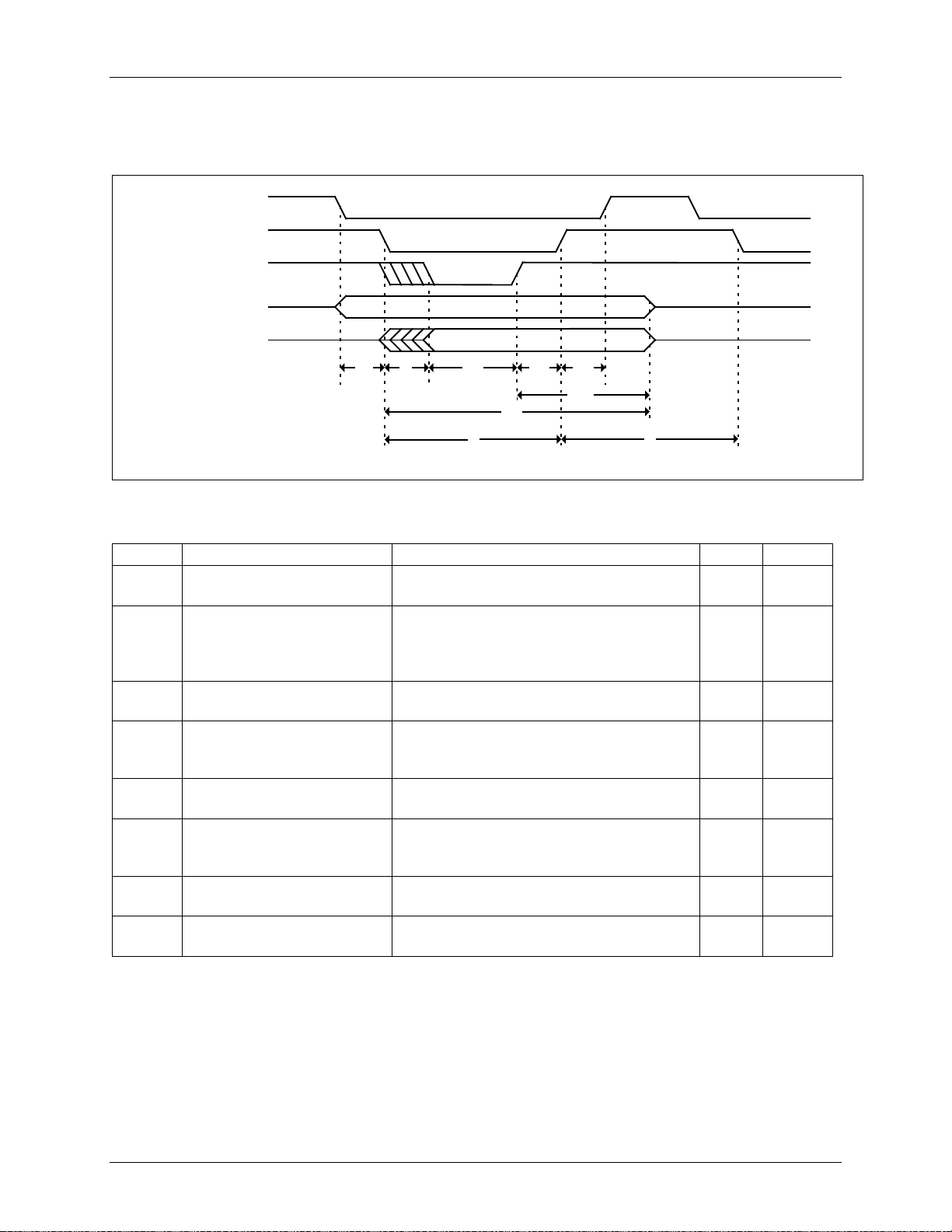
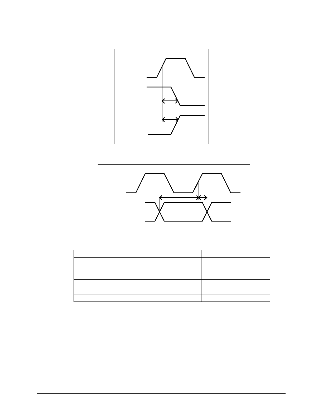
5 Host Interface Timing Specification
5.1 Host Interface
Figure 8: Host Interface Timing Diagram
T
SU
CS and ADDR setup time
CS and ADDR must be stable on or
before the falling edge of WR/OE.
T Output settling time
SL
The maximum amount of time that it will
take the MEMWAIT, or DATA when there
is no MEMWAIT, outputs to become
stable after the falling edge of WR/OE.
T Maximum wait time
WT
The maximum amount of time that the
MEMWAIT output will held asserted.
T Wait hold time
HWT
The minimum amount of time that the
WR/OE input must be held past the
de-assertion of MEMWAIT.
T
HCS
CS hold time
The CS input must be stable low for the
entire duration of the WR/OE low cycle.
T ADDR and DATA hold time
HO
The ADDR and DATA inputs must be
stable for no less than this amount of time
after the falling edge of WR.
T
L
WR/OE min low pulse
The minimum amount of time that the
WR/OE inputs must be held low.
T
H
WR/OE min high pulse
The minimum amount of time that the
WR/OE inputs must be held high.
Note: On read cycles when MEMWAIT is asserted the DATA outputs will be valid before the
de-assertion of MEMWAIT.
0 ns –
– 13.7 ns
– 17 ck
10 ns –
0 ns –
2.5 ck –
2 ck –
2 ck –
22 Rev. 1.2
DS_8430_001 78Q8430 Data Sheet
T
FALL
T
RISE
BUSCLK
Output
Delay
Output
Delay
BUSCLK
Input
T
SU
T
H
Parameter
Symbol
Min
Nom
Max
Unit
SU
H
FALL
RISE
WL
WH
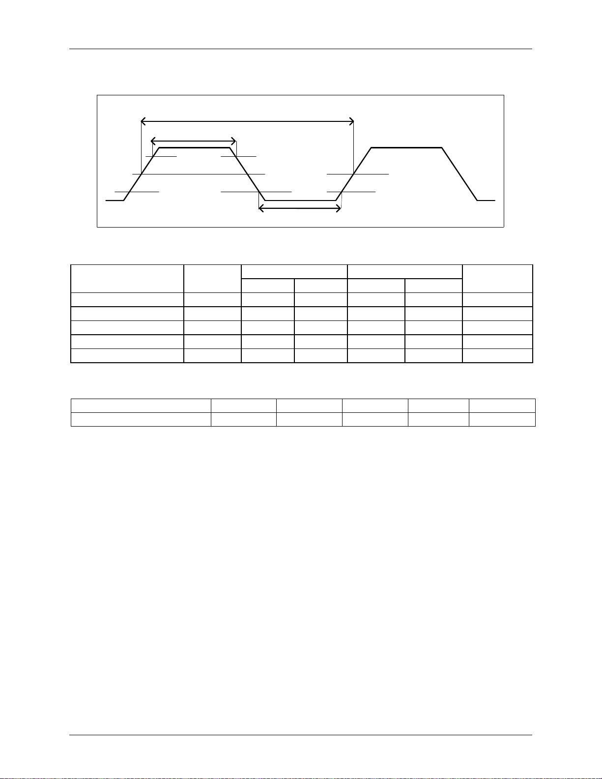
5.1.1 Synchronous Mode Timing
Figure 9: Host Bus Output Timing Diagram
Figure 10: Host Bus Input Timing Diagram
Input Setup Time T 6
Input Hold Time T 6
Output Fall Delay T –
Output Rise Delay T –
CSB min low P 1
CSB min high P 2
– – ns
– – ns
– 8 ns
– 8 ns
– – clk
– – clk
Rev. 1.2 23
78Q8430 Data Sheet DS_8430_001
T
CYC
T
HIGH
T
LOW
V
IH
V
IL
80%
50%
20%
CYC
Parameter
Symbol
Min
Nom
Max
Units
5.1.2 Bus Clock Timing
Figure 11: Bus Clock Timing
Parameter Symbol
BUSCLK Cycle Time T 20
– 10 – ns
BUSCLK Frequency – – 50 – 100 MHz
BUSCLK High Time T 8
BUSCLK Low Time T 8
– 3 – ns
HIGH
– 3 – ns
LOW
BUSCLK Slew Rate – 1 3 1 3 V/ns
Sync 50 Async 100
Min Max Min Max
Units
5.1.3 Reset Timing
RESETB Minimum Duration T 1
– – clocks
RESET
24 Rev. 1.2
DS_8430_001 78Q8430 Data Sheet
Bus
Control
EMI
Address
& Data
EMI
System
MAC MII
Transmit
MAC Half
Duplex
MAC
MII
Receive
MII
Register
Controller
EEPROM/
ROM
Control
Queue
Memory
Snoop
Controller
Network
Wake-up
Flow
Control
Queue
Read/Write
Logic
CAM
Packet
Classify
CTL
Controller
Memory
Manager
RMON
DMA Status
Register
TX/RX
Packet Status
Register
QUE Status
Register
MAC Status
Register
PROM_CS
PROM_CLK
PROM_DO
PROM_DI
4 Queue
Write Logic
1 Queue
Read Logic
JTAG
IEEE
1149.1
Boundary
Scan
TRSTB
TDO
TDI
TMS
TCLK
MEMWAIT
WRB/OEB
CSB
ENDIAN[1:0]
BOOTSZ[1:0]
WAITMODE
CLKMODE
BUSMODE
DATA
ADDR
PMEB
INTB
RESETB
BUSCLK
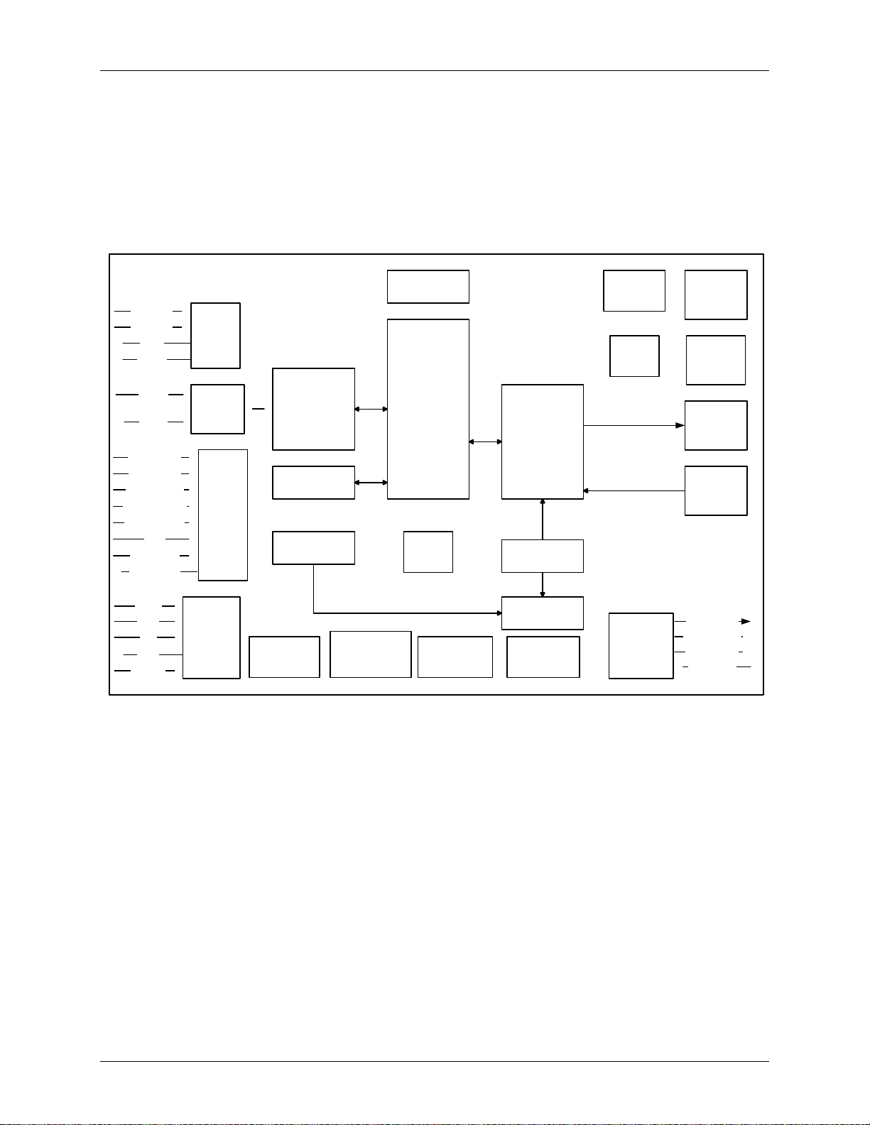
6 Functional Description
6.1 Internal Block Diagrams
6.1.1 Internal Digital Block
Figure 12 presents an overview of the functional layers of the 78Q8430. On the left side are the signals,
which connect to the GBI bus. On the upper and middle right, the blocks that implement the MAC sid e of
the MII are shown. These blocks are connected to the embedded PHY. On the lower right, connections
to the EEPROM are shown.
Figure 12: Internal Digital Block Diagram
6.1.2 Internal PHY
Figure 13 shows the functional blocks of the i nternal 78Q8430 PHY. The signals shown on the lef t side
are the internal MII signals to the MAC. These sig nals are multiplexed with their respective ex ternal pins
for use with an external PHY device. The 78Q8430 i s not a two-port device. Only one PHY interface can
be operational.
Rev. 1.2 25

78Q8430 Data Sheet DS_8430_001
MII
Transmit
Logic
4B/5B Encoder
Scrambler,
Parallel to Serial
100M
NRZ/NRZI
MLT3 Encoder
Pulse Shaper
and Filter
Parallel to Serial
Manchester
Encoder
Tx Clock
Generator
UTP
Driver
TXOP
TXON
UTP
Receiver
RXIP
RXIN
LED0
LED1
Auto
Negotiation
Clock
Recovery
Carrier Sense,
Collosion Detect
10M
Serial to Parallel
Descrambler,
5B/4B Decoder
Manchester
Decoder,
Serial to Parallel
100M
Clock
Reference
XTLP/CLKIN
XTLN
VCC GND
MII
Receive
Logic
MII
Activity
MII
Registers
Interrupt
Logic
10M
Adaptive Equalizer,
Baseline Wander,
MLT3 Decoder,
NRZI/NRZ
LED
Control
Logic
LINK
TXA
RXA
COLI
100BT
10BT
FDX
TX_CLK
TXD[3:0]
TX_EN
TX_ER
INTR
CRS
COL
RX_CLK
RXD[3:0]
RX_DV
RX_ER
MDC
MDIO
Figure 13: Internal PHY Block Diagram
On the right side are the signals, which con nect to the status LEDs and a 1:1 isolation transformer before
connecting to an RJ-45 connector, or equivalent m edia components.
6.2 Data Queuing
Ethernet frame data in the 78Q8430 is managed in q ueui ng structures called QUEs. The host bus
address space allocated for QUEs has enough space for eight, while the 78Q8430 circuit only
implements five. QUEs are identified numerically, QUE0 through QUE7, based on the registers in the
QUE register space that are used to access t hem . QUE1, QUE6 and QUE7 are unimplemented and
reserved for future use.
A QUE allocates main buffer memory as needed and stores discrete frames as they are written into the
QUE. The QUE then reads back frames in the sam e order that they were written and frees the mai n
buffer memory. A QUE can contain a maximum of 125 frames at any one time. If a QUE is unable to
allocate main buffer memory when writing a f rame, the frame will be partially added to the QUE as a
truncated frame. If a QUE is unable to allocat e m ai n buffer memory to start a frame, the entire fram e i s
dropped.
The QUEs are divided into two categories: re ceive QUEs, that store received frame data and transmit
QUEs, that store transmit frame data. Fram es are written to a receive QUE by the MAC and r ead out by
the host. Frames are written to a transmit Q UE by the host and read out by the MAC. QUE0 and QUE1
are receive QUEs (only QUE0 is implemented), and QUE2 through QUE7 are transmit QUEs (QUE2
through QUE5 are implemented). Writing to the Transmit Data Register (TDR) for a receive QUE or
reading from the Read Data Register (RDR) for a transmit QUE is not supported and the result is
undefined in this specification.
The transmit QUEs are further divided into standard QUEs, as described above, and static QU Es. Static
QUEs differ from the standard QUEs in that they can only contain a single frame, and that frame must be
252 bytes or less in total size. Unlike standard QUEs, static QUEs do not remove a frame when it i s read
from the QUE. Once a frame is written to a stati c QUE, it can be read out any number of times and the
static QUE will always read out the same one frame. If a second frame is written to a static QUE then it
will replace the first as the one frame contained in the QUE.
26 Rev. 1.2

DS_8430_001 78Q8430 Data Sheet
The purpose of a static transmit QUE is to allow t he host to configure a frame that will need to be
transmitted multiple times or transmitted at a later time without any interaction with the host. Transmit
QUE2 and QUE5 are static QUEs. Transmit QUE2 is best suited for MAC control pause fra m es as it can
be triggered to transmit by a main buffer watermark. Transmit QUE5 is best suited to Host Not
Responding (HNR) frames as it can be triggered to transmit by a host interrupt timeout.
When the MAC transmitter is idle and ready t o transmit a frame, it determines which QUE to re ad from on
a priority basis. The lowest numbered QUE contai ni ng data that needs to be transmitted is select ed by
the MAC, which means when more than one transmi t QUE is ready, the one with the lowest number
always gets priority.
6.3 Host Interface
6.3.1 Reading Receive Data
The status of the frame at the top of the receive FIFO can be obtained by reading the Receive Packet
Status Register (RPSR). The 16 LSBs of the RPSR contain a count of the total number of bytes that
have entered the receive FIFO for this frame. A value of zero means that there are no new frames in the
receive FIFO. As frame bytes enter the FIFO, the count value is incremented. However, the count value
does not decrease the bytes read out of the read FI F O such that the final value will always be the final
frame size.
The MSB of the RPSR is the DONE bit. Once the last byt e in the frame has entered the receive FIFO,
the DONE bit is set indicating that the co unt value contained in the total bytes field now contai ns t he final
size in bytes of the frame and the error status and classification fields now contain the final frame st atus.
When the DONE bit is asserted, this also indi cat es that the status for this frame has been removed from
the receive status FIFO and future reads of t he RPSR will ref er to the next frame in the receive FIFO,
even if all of the data for the current frame has not been retrieved.
The frame data is read from the receive FI FO 32 bits at a time by successive reads to the Receive Data
Register (RDR). If the frame length is not an even multiple of 4 bytes then the final read of the RPDR
register for that frame will be padded wit h zeros.
6.3.2 Writing Transmit Data
A transmit QUE is initialized by writing to its Packet Control Word Register (PCWR). This will assign an
ID to the frame and select various transmission opt i ons. The frame size must then be set by writing to the
QUE Packet Size Register (PSZR). Transmit data is then written to the transmit FIFO 32 bits at a time via
successive writes to the Transmit Data Register (TDR).
If more bytes are written to the TDR than indicate d n the PSZR, the excess bytes are ignored. Writes to
the TDR past the end of the frame, however, will trigger a transmit FIFO overrun interrupt condition.
Similarly, if a new frame is initialized by a write to the PCWR before the frame length counter is expired, a
transmit FIFO under-run interrupt condition wil l result and the previous frame will be aborted. If there is
any question, the PSZR can be queried for the remaining number of bytes expected in the previous frame
before a new frame is initialized.
In the event that the host wishes to terminate a frame early without triggering an under-run interrupt and
aborting the frame, or if the size of the frame is not initially known, the PSZR can be rewritten at any time
before the end of the frame’s transmission. As an example, no matter what the current value of the PSZR
is, if it is written with a value of one then t he next write to the TDR will add one byte to the completed
frame. Conversely, if the frame byte count er i s about to expire then writing a larger value to the PSZR will
extend the frame. It is an error to write a val ue of zero to the PSZR and the circuit behavior in this case is
undefined.
As each frame egresses the transmit FIFO, its status is placed in the transmit status FIFO. Transmit
frame status is recovered by reading the Transmit Packet Status Register (TPSR). The Packet ID field
from the PCWR is also placed in the TPSR such that the status can be ass ociated with the exact frame to
which it belongs.
Rev. 1.2 27
 Loading...