

TERIDIAN Semiconductor 78Q8392L User Manual
78Q8392L/A03
r
Low Power Ethernet
Coaxial Transceive
November 2008
DESCRIPTION
The 78Q8392L/A03 Ethernet Transceiver is a
replacement for the SSI/TDK/Teridian
78Q8392L/A02 coax line transmitter/receiver. Only a
single resistor value change is required for
upgrading an existing 78Q8392L/A02 design to the
78Q8392L/A03.
The device includes analog transmit and receive
buffers, a 10 MHz on-board oscillator, timing logic
for jabber and heartbeat functions, output drivers
and bandgap reference, in addition to a current
reference and collision detector.
This transceiver provides the interface between the
single-ended coaxial cable signals and the
Manchester-encoded differential logic signals.
Primary functional blocks include the receiver,
transmitter, collision detection and jabber timer. This
IC may be used in either internal or external MAU
environments.
The 78Q8392L/A03 is available in lead-free 16-pin
plastic and 28-pin PLCC packages.
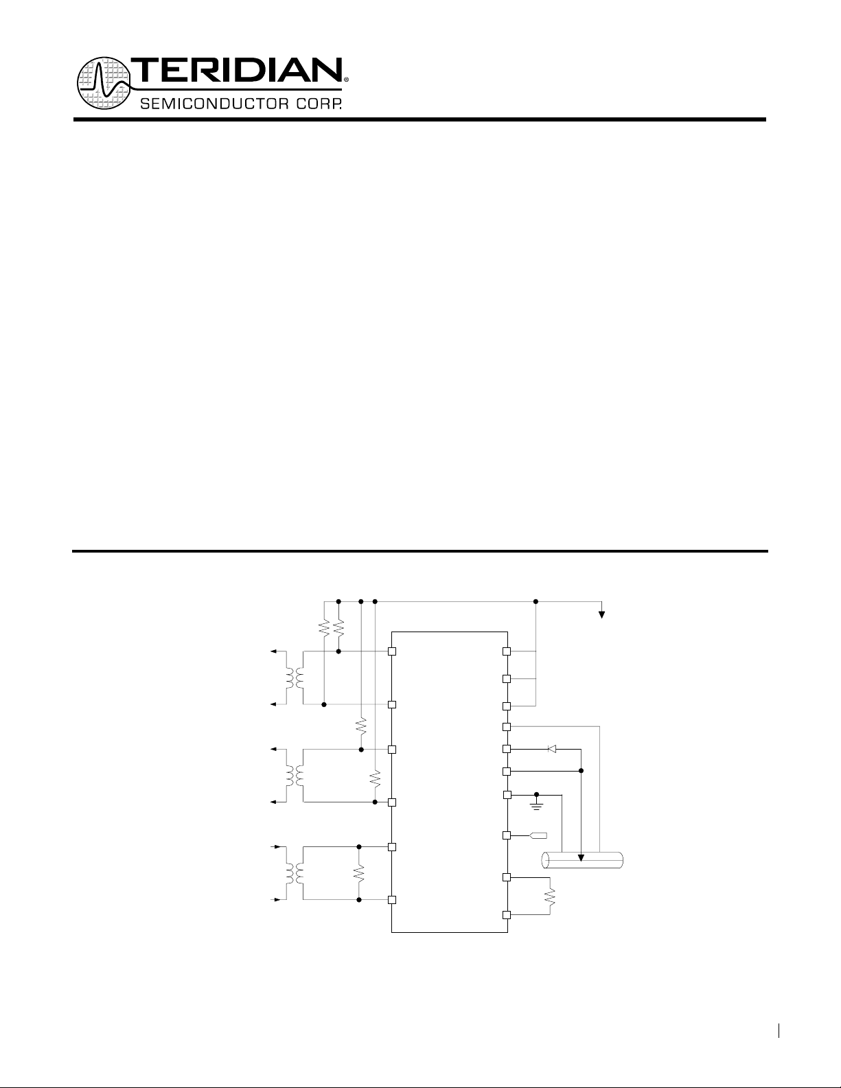
CONNECT DIAGRAM
FEATURES
• Very low power consumption
• Compliant with Ethernet II, IEEE 802.3
10Base5 and 10Base2
• Integrates all transceiver functions except
signal and power isolation
• Innovative design minimizes external
component count and power consumption
• Jabber timer function integrated on chip
• Externally selectable CED heartbeat allows
operation with IEEE 802.3 compatible
repeaters
• Squelch circuitry at all inputs rejects noise
• Power-on reset and test modes
• Advanced BiCMOS process
DATA FROM
510 ±5%
COLLISION
SIGNAL
TO DTE
DATA TO
DTE
DTE
x 4
78
–9V
41
CD+
2
CD–
3
RX+
6
RX–
7
TX+
8
TX-
VEE
VEE
VEE
CDS
TXO
RXI
GND
HBE
RR-
RR+
5
13
16
15
14
10
9
12
11
COAX
Page: 1 of 14 © 2008 Teridian Semiconductor Corporation Rev 1.3

FUNCTIONAL DESCRIPTION
The 78Q8392L/A03 incorporates six basic functions
of the Ethernet Transceiver, including receiving,
transmitting, collision signaling, collision detection,
jabber timing, and the heartbeat function. Refer to
Figure 1 for a general system block diagram.
RECEIVER FUNCTIONS
The receiver senses signals through the RXI input,
which minimizes reflections on the transmission
media using a low capacitance, high resistance
input buffer amplifier. The CDS ground input
attaches directly to the input buffer from the coaxial
shield to eliminate ground loop noise.
In addition to the input buffer, the receiver data path
consists of an equalizer, data slicer, receiver
squelch circuitry, and an output line driver.
The equalizer improves the cable-induced jitter; the
data slicer restores equalized received signals to
fast transition signals with binary levels to drive the
receiver line driver; and the receiver line driver
drives the AUI cable through an isolation transformer
that connects to the AUI interface.
Noise on the transmission media is rejected by the
receiver squelch circuitry, which determines valid
data via three criteria: Average DC level, pulse
width and transition period. The DC voltage level is
detected and compared to a set level in the receiver
comparator circuit. The pulse width must be greater
than 20 ns to pass the narrow pulse filter; the
transition timer outputs a true level on the RX Data
Valid line provided the time between transitions is
less than about 200 ns. As long as a valid RXI signal
is detected, the output line driver remains enabled.
The transition timer disables the line driver when
there are no further transitions on the data medium,
and the RX+, RX- pins go to a zero differential
voltage state (Figure 3).
TRANSMITTER FUNCTIONS
The transmitter data path consists of a transmit input
buffer, pulse-shaping filter, transmit s quelch
circuitry and transmit output line driver. The
self-biasing transmit input buffer receives data
through an isolation transformer and translates the
AUI differential analog signal to a square pulse
suitable for driving the pulse shaping filter.
78Q8392L/A03
Low Power Ethernet
Coaxial Transceiver
The filter outputs a correctly shaped and band
limited signal to the transmit output driver, which
drives the transmission medium through a high
impedance current source. When the transmitter is
off, the capacitance of the transmit driver is isolated
from the transmission media by an external diode
with a low capacitance node. The shield of the
transmission media serves as the ground return for
the transmitter function.
A transmit squelch circuit, which consists of a pulse
threshold detector, a pulse width detector, and a
pulse duration timer, is used to suppress noise, as
well as crosstalk on the AUI cable. The squelch
circuitry disables the transmit driver if the signal at
TX+ or TX- is smaller than the pulse threshold.
Pulse noise is rejected by a pulse width detector that
passes only pulses with durations greater than 20
ns. The pulse duration timer disables the transmit
driver if no pulses are received for two-bit periods
following valid pulses. At the end of a transmission,
the pulse duration timer disables the transmitter and
triggers the blanking timer, used to block “dribble”
bits.
COLLISION DETECTION
A collision occurs when two or more transmitters
simultaneously transmit on the transmission media.
A collision is detected by comparing the average DC
level of the transmission media to a collision
threshold. The received signal at RXI is buffered and
sent through a low pass filter, then compared in the
collision threshold circuit. If the average DC level
exceeds a collision threshold, a 10 MHz signal is
output on the CD± pins.
COLLISION SIGNALING
When collision signaling is enabled (HBE pin is high
and the average DC level on RXI exceeds the
collision threshold V
the CD± pins through an isolation transformer to the
DTE. When the function is disabled, this output goes
to a zero differential state. The 10 MHz signal output
from the CD± pins indicates a collision on the
transmission media, a heartbeat function, or that the
transmitter is in jabber mode.
), a 10 MHz signal is sent from
CD
Page: 2 of 14 © 2008 Teridian Semiconductor Corporation Rev 1.3
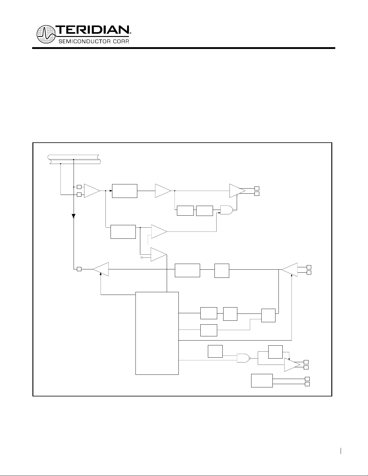
JABBER FUNCTION
When valid data on the TX± pins is detected, the
jabber timer is started. If there is valid data for more
than 20 ms, a latch is set which disables the
transmitter output and enables the 10 MHz output on
the CD± pins. The latch is reset within 0.5 seconds
after the valid data is removed from the transmitter
input (TX±). This action resets the jabber timer and
disables the 10 MHz signal on the CD± pins. The
TX± inputs must remain inactive during the 0.5
second reset period.
DATA MEDIA
CDS
TXO
RXI
RECEIVER
INPUT
BUFFER
TRANSMIT
OUTPUT DRIVER
TX ON
EQUALIZER
LP FILTER
COLLISION
THRESHOLD
COMPARATOR
SQUELSH
THRESHOLD
CONTROL LOGIC
JABBER TIMER
BLANKING TIMER
HEART BEAT TIMER
SLICER
SQUELCH
COLLISION
COMPARATOR
78Q8392L/A03
Low Power Ethernet
Coaxial Transceiver
HEARTBEAT FUNCTION
The 10 MHz CD outputs are enabled for about 1 µs
at approximately 1.1 µs after the end of each
transmission. The heartbeat signal tells the DTE that
the circuit is functioning. This is implemented by
starting the heartbeat timer when the valid data
signal indicates the end of a transmission. This
function is disabled when HBE pin is tied to V
RX+
RX-
RX DATA
TRANSITION
PERIOD
TAMER
TRANSITION
PERIOD
TIMER
TRANSITION
END
TIMER
VALID
10 MHz
OSC
SLICER
NARROW
PULSE
FILTER
ENABLE
BUFFERED TX
TX ± > -250 mV
TX ± < -250 mV
BANDGAP
REFERENCE
AND CURRENT
REFERENCE
COMPARATOR
SIGNAL
PRESET
DETECT
TRANSMIT INPUT
BUFFER
TX DISABLE
ENABLE
NARROW
PULSE
FILTER
PULSE
SHAPING
FILTER
TX DATA VALID
END TRANSMIT
TX± DISABLE
CD ± ON
CD+
CD-
RR+
RR-
EE.
TX+
TX-
FIGURE 1: 78Q8392L/A03 General System Block Diagram
Page: 3 of 14 © 2008 Teridian Semiconductor Corporation Rev 1.3
78Q8392L/A03
Low Power Ethernet
Coaxial Transceiver
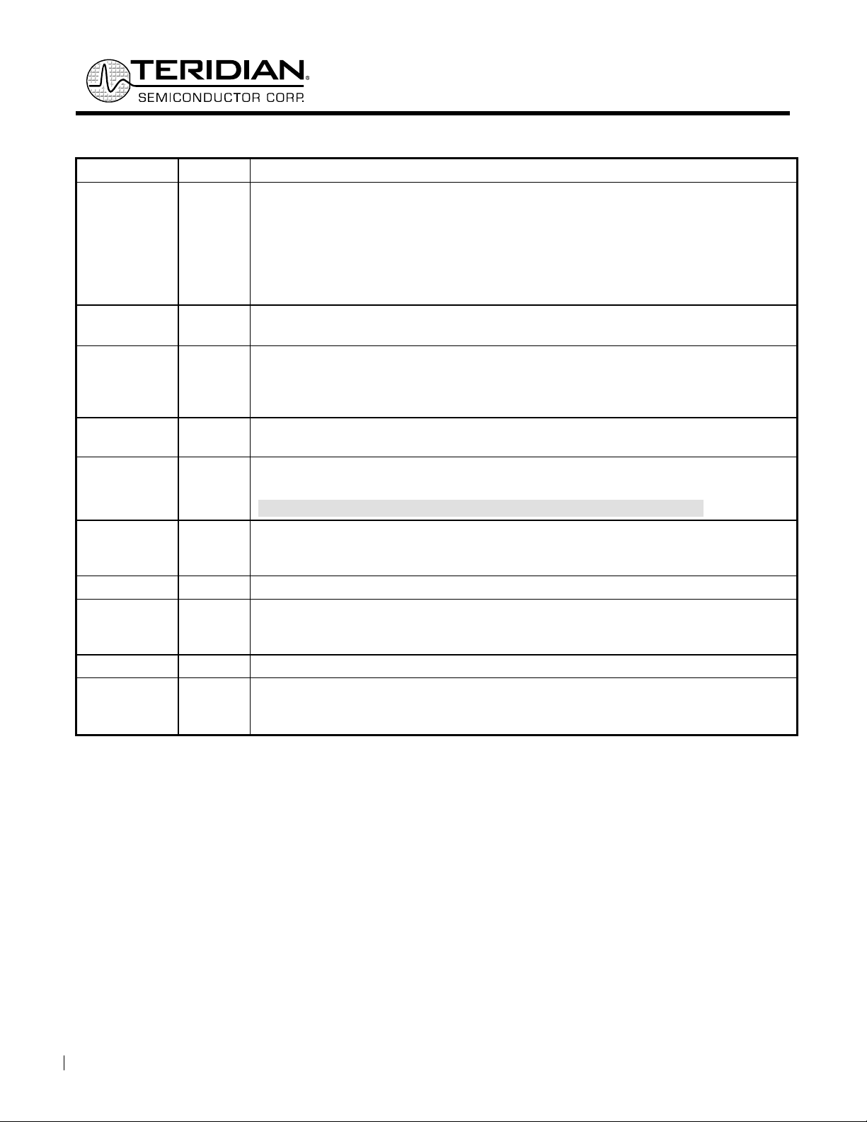
PIN DESCRIPTION
NAME TYPE DESCRIPTION
Collision Output. Balanced differential line driver outputs from the collision detect
circuitry. The 10 MHz signal from the internal oscillator is transferred to these
outputs in the event of collision, excessive transmission (jabber), or during CD
CD+*/CD- O
RX+*/RX- O
TX+*/TX- I
HBE I
RR+/RR- I
RXI I
TXO O Transmit Output. Connects via an isolation diode to the coaxial cable.
CDS I
GND S Positive Supply Pin.
VEE S
*IEEE names for CD± = CI±, RX± = DI±, TX± = DO±
Notes: Pin type: I-input; O-output; S-power supply
Heartbeat condition. These outputs are open emitters; pulldown resistors to VEE are
required. When operating into a 78Ω transmission line, these resistors should be
510Ω. In Cheapernet applications, where the 78Ω drop cable is not used, higher
resistor values (up to 1.5k) may be used to save power.
Receive Output. Balanced differential line driver outputs from the Receiver. These
outputs also require 510Ω pulldown resistors.
Transmit Input. Balanced differential line receiver inputs to the Transmitter. The
common mode voltage for these inputs is determined internally and must not be
externally established. Signals meeting Transmitter squelch requirements are
waveshaped and output at TXO.
Heartbeat Enable. This input enables CD Heartbeat when grounded or left opened,
disables it when connected to VEE.
External Resistor. A fixed 976Ω 1% resistor connected between these pins
establishes internal operating currents.
Note: The previous generation 78Q8392L/A02 used a 1kΩ 1% resistor
Receive Input. Connects directly to the coaxial cable. Signals meeting Receiver
squelch requirements are equalized for inter-symbol distortion, amplified, and output
at RX+ and RX- pins.
Collision Detect Sense. Ground sense connection for the collision detect circuit. This
pin should be connected separately to the shield to avoid ground drops from altering
the receive mode collision threshold.
Negative Supply Pins. These pins should be connected to a large metal frame area
on the PC board to handle heat dissipation, and bypassed to the GND pin with a
0.1µF capacitor as close to the package as possible.
Page: 4 of 14 © 2008 Teridian Semiconductor Corporation Rev 1.3
78Q8392L/A03
Low Power Ethernet
Coaxial Transceiver
ELECTRICAL SPECIFICATIONS
ABSOLUTE MAXIMUM RATINGS
Absolute maximum ratings indicate limits beyond which permanent damage may occur. Continuous operation at
these limits is not recommended; operations should be limited to those conditions specified under recommended
operating characteristics.
PARAMETER RATING
Supply Voltage -10V
Input Voltage 0 to VEE
Storage Temperature
Soldering (Reflow or Dip)
Package power dissipation
DC OPERATING CHARACTERISTICS
0°C ≤ T (ambient) ≤ +70°C, VEE = -9V ± 5%
-65 to 150°C
235°C for 10 sec
1.0 watts @ 25°C
PARAMETER
I
EE1
V
I
EE2
V
I
RXI
Supply current out of
pin - non-transmitting
EE
Supply current out of
pin - transmitting
EE
Receive input bias
CONDITION MIN NOM MAX UNIT
6 8 mA
50 65 mA
See Note 3 -2 +25 µA
current (RXI)
I
TDC
Transmit output dc
See Note 4 37 41 45 mA
current level (TXO)
I
TAC
Transmit output ac
See Notes 4 & 5 ±28 I
current level (TXO)
V
CD
Collision threshold
See Note 9 -1.58 -1.52 -1.404 V
(Receive mode)
V
OD
Differential output voltage
See Notes 3 & 7 ±550 ±1200 mV
(RX±, CD±)
V
OC
Common mode output
See Note 3, 6 & 7 -3.0 -2.5 -2.0 V
voltage (RX±, CD±)
V
OB
Differential output voltage
See Notes 3, 7 & 8 ±40 mV
imbalance (RX±, CD±)
V
TS
Transmitter squelch
-340 -260 -200 mV
threshold (TX±)
C
X
R
RXI
Input capacitance (RXI)
Shunt resistance –
1.2 pF
See Note 3 100 150
non-transmitting (RXI)
R
TXO
Shunt resistance –
See Note 4 200
transmitting (TXO)
mA
TDC
kΩ
kΩ
Page: 5 of 14 © 2008 Teridian Semiconductor Corporation Rev 1.3
 Loading...