

TERIDIAN Semiconductor 78Q2123, 78Q2133 User Manual
78Q2123/78Q2133 MicroPHY™
TX Transceiver
Simplifying System IntegrationTM
SMI
TXD
RXD
TXC
RXC
MII
Registers
4B/5B Encoder,
Scrambler,
Parallel/Serial
Parallel/Serial,
Manchester Encoder
Manchester Decoder,
Parallel/Serial
Serial/Parallel
Descrambler,
5B/4B Decoder
MRZ/NRZI
MLT3 Encoder
TX CLK GEN
Carrier Sense,
Collision Detect
CLK
Recovery
Clock Reference
10M
CLKIN
25MHz
Pulse Shaper
and Filter
Auto
Negotiation
Adaptive EQ,
Baseline Wander Correct,
MLT3 Decode, NRZI/NRZ
LEDs
Link Act
Auto
MDI-X
Mux
10M 100M
Rx/Tx
Tx/Rx
MII
100M
10/100BASE-
DESCRIPTION
TM
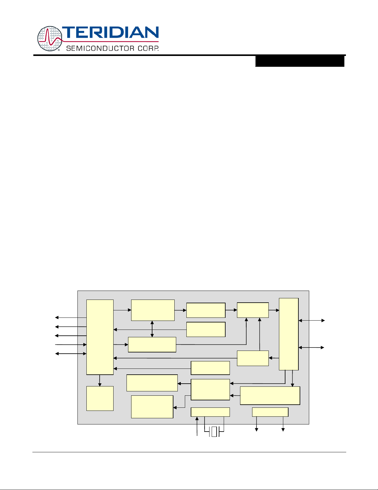
The 78Q2123 and 78Q2133, MicroPHY
, are the
smallest 10BAS E-T/100BASE-TX F ast Ethernet
tran sceivers in the mark et. They inclu de integrated
MII, ENDECs, scrambl er /descrambler , dual-speed
clock recovery, and full-featured auto-negotiation
functions. The tran smitter includes an on-chip pulseshaper and a low-power line driver. The receiver has
an ad aptive equalizer and a baseline restorat i on
circuit requir ed for accurate c lock an d data recovery.
The transceiver interfaces to C ategory-5 unshielded
twisted pai r ( C at-5 UTP) cabling for 100BASE-TX
app l ications, and Category-3 unshielded twisted pair
(Cat-3 UTP) for 10BASE-T applications . The MDI is
connected to th e l ine med ia via dual 1:1 i solation
tran sformers. No e xt er nal filter i s required. Interface
to the MAC is accomplished through an I EEE-802.3
compliant Med i a Independent Interface ( M II). The
78Q2123/78Q2133 are in tended to serve t he
embedded Ethernet mark et, tailored s pecific ally to the
need s of gam e consol es, b r oadband modems,
printers, set top boxes and audio/visual equipment. It
is d esigned for low-power consumption and operates
from a single 3.3V supply. The 78Q2123 is rated for
commerci al temperature range and th e 78Q2133 is
rated for indust r i al tem perature range.
DATA SHEE T
April 2010
FEATURES
• Smallest 10/ 10 0 PH Y avai l a bl e
• 10BASE-T/100BASE-TX IEEE-802.3 compliant
TX and RX fun ctions requi r ing a du al 1:1 isolation
tran sformer i nterface to t he line
• Integrate d MI I, 10 BA SE-T/100BASE-TX ENDEC,
100BASE-TX scrambler/descrambler , and
full-featured auto-negotiation function
• Full duplex operation cap able
• Automatic MDI/MDI-X cros s over correction
• Register-programmable transmit amplitude
• Au tomatic polarity correction du r ing auto-
negotiation and 10BASE-T signal reception
• Power-sav ing and power -down modes including
transmitter d isable
• 2 Programmable LED indicators (Link and
Activity by default)
• User programmable Interrupt pin
• Package: 32-QFN (5x5 mm)
• Low Power (~290mW)
• Single 3.3 V ± 0.3V Supply
• 78Q2123 rated for 0°C to 70°C operation
• 78Q2133 rat ed for -40°C to 85°C operation
Rev. 1.6 © 20 10 Teridi an Semiconductor Cor porati on 1

78Q2123/78Q2133 Data Sheet DS_21x3_001
Table of Contents
1 Functional Description .................................................................................................................. 5
1.1 General ................................................................................................................................... 5
1.1.1 Power Management .................................................................................................... 5
1.1.2 An al og Biasing and Supp l y Regulation ........................................................................ 5
1.1.3 Clock Selection............................................................................................................ 5
1.1.4 Transmit Clock Generation .......................................................................................... 5
1.1.5 Receive Signal Qualification ........................................................................................ 6
1.1.6 Receive Clock Recovery.............................................................................................. 6
1.2 100BASE-TX OPERATION ..................................................................................................... 6
1.2.1 100BASE-TX Transmit ................................................................................................ 6
1.2.2 100BASE-TX Recei ve ................................................................................................. 6
1.2.3 PCS Bypass Mode (Auto-negotiate must be off) .......................................................... 6
1.3 10BASE-T OPERATION ......................................................................................................... 7
1.3.1 10BASE-T Transmit..................................................................................................... 7
1.3.2 10BASE-T Receive...................................................................................................... 7
1.3.3 Polarity Correction ....................................................................................................... 7
1.3.4 SQE TEST .................................................................................................................. 7
1.3.5 Natural Loopback ........................................................................................................ 7
1.3.6 Repeater Mode............................................................................................................ 7
1.4 Auto-Negotiation ..................................................................................................................... 8
1.5 Media Independent Interface ................................................................................................... 9
1.5.1 MII Transm it and R eceive Operation ............................................................................ 9
1.5.2 Station Management In terface ..................................................................................... 9
1.6 Add i tional Featur es ............................................................................................................... 10
1.6.1 LED Indicators ........................................................................................................... 10
1.6.2 Interrupt Pin............................................................................................................... 10
1.6.3 Automatic MDI/ MDI-X Con figuration ......................................................................... 10
2 Pin Description ............................................................................................................................ 11
2.1 Legend ................................................................................................................................. 11
2.2 MII ( M edia Independent Interface) ......................................................................................... 11
2.3 Control and Status ................................................................................................................ 12
2.4 MDI (Media Depend ent In terface).......................................................................................... 12
2.5 Oscillator/Clock ..................................................................................................................... 12
2.6 Power Supply and Ground .................................................................................................... 12
2.7 LE D Si gnals (Program mabi lity Is Secondary Requirement).................................................... 13
3 Register Description ................................................................................................................... 14
3.1 MR0: Control Register ........................................................................................................... 15
3.2 MR1: Status Register ............................................................................................................ 16
3.3 MR2: PHY Ident ifier Register 1 .............................................................................................. 17
3.4 MR3: PHY Ident ifier Register 2 .............................................................................................. 17
3.5 MR4: Auto-Negotiation Ad vertisement Register ..................................................................... 17
3.6 MR5: Auto-Negotiation Link Partner Ab ility Register ............................................................. 18
3.7 MR6: Auto-Negotiation Expansion Register ........................................................................... 18
3.8 MR16: Vend or Spec i fi c Register ............................................................................................ 18
3.9 MR17: Interrupt Control/Status Register ................................................................................ 20
3.10 MR18: Diagnost ic Reg is ter .................................................................................................... 21
3.11 MR19: Transceiver C ontrol................................................................................................... 21
3.12 MR20: Res er ved ................................................................................................................... 21
3.13 MR21: Res er ved ................................................................................................................... 21
3.14 MR22: Res er ved ................................................................................................................... 21
3.15 MR23: LED Configuration Register........................................................................................ 22
3.16 MR24: MDI/MDIX Cont rol Regis ter ........................................................................................ 22
2 Rev. 1.6

DS_21x3_001 78Q2123/78Q2133 Data Sheet
4 Electrical Specifications .............................................................................................................. 23
4.1 Absolute Maximum Ratings ................................................................................................... 23
4.2 Recommended Operating Condi tions .................................................................................... 23
4.3 DC Characteristics ................................................................................................................ 23
4.4 Digital I/O Characteristics ...................................................................................................... 24
4.5 Digital Timing Characteristics ................................................................................................ 25
4.5.1 RST Characteristics................................................................................................... 25
4.5.2 MII Transmit Interface ................................................................................................ 25
4.5.3 MII Receive Inter fac e ................................................................................................. 26
4.6 MDIO Interfac e Input Timing ................................................................................................. 26
4.6.1 MDIO Interface Output Timing ................................................................................... 27
4.6.2 MDIO Interface Output Timing ................................................................................... 28
4.6.3 100BASE-TX System Timing ..................................................................................... 29
4.6.4 10BASE-T S yst em Timing ......................................................................................... 29
4.7 An al og Electric al Characteristics ........................................................................................... 30
4.7.1 100BASE-TX Transmitt er .......................................................................................... 30
4.7.2 100BASE-TX Trans mit ter (Informative) ...................................................................... 30
4.7.3 100BASE-TX Recei ver .............................................................................................. 30
4.7.4 10BASE-T Transmitter............................................................................................... 31
4.7.5 10BASE-T Transmitter (Informat i ve) .......................................................................... 31
4.7.6 10BASE-T Receiver .................................................................................................. 31
4.8 Isolation Transformers........................................................................................................... 33
4.9 Reference Crystal ................................................................................................................. 33
4.9.1 External XTLP Oscillat or C haracteristics .................................................................... 34
5 Package Pin Designations .......................................................................................................... 35
6 32-Pin QFN Mechanical Specifications ....................................................................................... 36
6.1 Recommended Pcb Land P attern Di mensions ....................................................................... 37
6.1.1 Recommended PCB Land Pattern D imensi ons .......................................................... 37
7 Ordering Information ................................................................................................................... 37
Revision H istory .................................................................................................................................. 38
Rev. 1.6 3

78Q2123/78Q2133 Data Sheet DS_21x3_001
Figures
Figure 1: RST Pulse Duration ................................................................................................................ 25
Figure 2: Transmit Inputs to the 78Q2123/78Q2133
Figure 3: Receive Outputs from the 78Q2123/78Q2133
Figure 4: MDIO as an Input to the 78Q2123/78Q2133
Figure 5: MDIO as an Output to the 78Q2123/78Q2133
Figure 6: MD IO Inter face Output Timin g
Figure 7: Application Diagram for 78Q2123/78Q2133
Figure 8: External XTLP Oscillator Characteristics
Figure 9: Package Pin Designat ions
Figur e 10: 32-Pin QFN M echan ical Specifications
............................................................................... 25
......................................................................... 26
............................................................................ 26
......................................................................... 27
................................................................................................. 28
............................................................................ 32
................................................................................. 34
...................................................................................................... 35
.................................................................................. 36
4 Rev. 1.6

DS_21x3_001 78Q2123/78Q2133 Data Sheet
1 Functional Description
1.1 General
1.1.1 Power Management
The 78Q2123 and 78Q2133 have three power saving modes:
• Chip Po wer-Down
• Receive Power M anagement
• Transmit High Impedance Mode
Chip po wer-down is activated by setting the PWRDN bit in MII register MR0.11. When the chip is in
power-down mode, all on-chip circuitry is shut off, and the device consumes minimum power. While in
the power-down state, th e 78Q2123/78Q2133 still respond to management transactions.
Receive power management (RXCC mode) i s activat ed by setting the RX CC bit in MII register M R16.0.
In this mode of operat i on, the adaptive equalizer, the cloc k recovery phase lock l oop (PLL), and all other
receive circuit r y will be powered down when no valid MLT-3 signal is present at the UTP receive line
interface. As s oon as a valid sig nal is detected, all circuits will au tomatically be powered up to resume
normal operation. Duri ng this mode of op er ation, RX_CLK will be inactive wh en there is no data being
received. Note t hat th e RX C C mode is not sup ported during 10BAS E-T operation.
Transmit high impedance mode is activated by setting the TXHIM bit in MII register MR16.12. In this
mode of operati on, the tr ansmit UTP dr i vers are in a high impedance state an d TX_CLK is tri-s tated. A
weak intern al pul l -up is enabled on TX_CLK. The receive cir cuitry remains fully operational. Th e default
state of MR16.12 i s a logic low for disabling the transmit hi gh impedance mode. Only a r eset condition will
automati cally cle ar M R16 .12. The tran smitter is fully func tional when MR16.1 2 i s cleared. This feature is
useful when configuring a system for W ake-On LAN (when the 78Q2123/78Q 2133 are coupled with a
Wake-On LAN capable MAC).
1.1.2 Analog Biasing and Supply Regulation
The 78Q212 3/78Q 2133 require n o ext er nal component to generate on-chip bias voltages and currents.
High accuracy is maintai ned through a closed-loop trimmed biasing network.
On-chip di gital logic r uns off an i nternal voltage regulat or . Hence only a single 3.3V (± 0.3V) supply is
required to power-up the device. The on-chip regulator is not affected by the power-down mode.
1.1.3 Clock Selection
The 78Q2123/7 8Q2133 have an on-chip crystal oscil lator which can also be driven by an external oscillator.
In this mode of operation, a 25 MHz crystal should be connected between the XTLP and XTLN pins.
Alt ern ati vely, an ext er nal 25 MHz clock input can be connected to the XTLP pin. In this mode of operation,
a crystal is not req ui r ed an d the XT LN pin must be tied to ground.
1.1.4 Transmit Clock Generation
The transmitter uses an on-chip frequency synthesizer to generate the transmit clock. In 100BASE-TX
operat ion, the synthesizer multiplies the referenc e clock by 5 to obtain the internal 125 MHz serial transmit
clock. In 10BASE-T mode , i t gene r a te s an i n te r nal 20 M H z tra nsmit cl ock by m ulti pl yin g t he re ference
25 MHz clock by 4/5. The synthesizer references either the local 25 MHz crystal oscillator, or the extern ally
applied clock, depending on the selected mode of operation.
Rev. 1.6 5

78Q2123/78Q2133 Data Sheet DS_21x3_001
1.1.5 Receive Signal Qualification
The integrate d signal qualifier has separa te squel ch and uns quelch threshol ds. It also includes a built-in timer
to ensure fast and accurate signal detection and line noise reject i on. Upon detection of two or more valid
10BASE-T or 100BASE -TX pulses on the line receive port, si gnal detect is indicated. T he signal detect
threshol d is then lowered by about 40% . All adaptive circui ts are released from their i nitial states and allow ed
to lock onto the i ncoming da ta. In 100BASE-TX operation, signal detect is de-asserted whe n no signal is
presented for a perio d of about 1.2 µs. In 10BASE-T operat ion , sign al detec t is d e-asserted whenever no
Manchester data is receive d. In either case, the signal detec t thres hold will retur n to the squelched level
whenever the signal detect indicatio n is de-asserted. Signal detect is also used to control the operation of the
clock/data recovery circuit to assure fast acquisition.
1.1.6 Receive Clock Recovery
In 100BASE-TX mode, the 125 MHz receive clock is extracte d using a di gital DLL-base d loo p. When no
receive signal is present, the CDR is directed to lock onto the 125 MHz transmit serial clock. When signal
detect is asserted, the CDR will use the received MLT-3 signal as the clock reference. The recovered clock is
used to re-time the data signal and for conversion of the data to NRZ format.
In 10BASE-T mode, the 20 MHz receive clock is recovered digi tally from the Manchester d ata us i ng a
DLL locked to t he reference clock. When Manchester-coded preambles are det ected, the CDR
immediatel y re-aligns the phase of the cl ock to s ynchronize wit h the incom ing d ata. Hence clock
acquisition is fast and immediate.
1.2 100BASE-TX OPER ATION
1.2.1 100BASE-TX Transmit
The 78 Q2123/78Q2133 contain al l of the necessar y c i r cuitry to convert the tr ansmit MII signali ng from a
MAC to an IEEE-802.3 compliant data-st r eam dr i ving Cat-5 UTP cabling. The internal PCS int er fac e
maps 4 bit ni bbles from th e M II to 5 b i t code g r oups as defined in Table 24-1 of IEEE-802.3. These 5 bit
code groups are then scram bled and con verted to a serial stream before being sent to the ML T-3 pulse
shaping circuitry and line driver. The pulse-shaper uses cu r r ent modulation to produce the desired output
waveform. Controlled rise/fall time in the MLT-3 s i gnal is achieved using an accurately controlled vo ltage
ramp generator. The li ne dri ver requires an external 1:1 isolation transformer to interface with the li ne
media. The c enter-t ap of the primar y side of the transformer must be connected to the Vcc supply (3.3V
± 0.3V).
1.2.2 100BASE-TX Receive
The 78Q2123/78Q2133 receive a 125MBaud MLT-3 signal through a 1:1 transformer. The signal then
goes through a combination of adaptive offset adjus tment (basel ine wander correction) and adaptive
equ al ization. The effect of thes e circuits i s to sense the amount of d ispersion and attenuat ion caused by
the cable and transformer , and restore the rec eived puls es to logic levels. The am ount of gain and
equ al ization applied to the pu lses varies with the detect ed attenuati on and dispers i on and, ther efore, with
the length of the cable. The 78Q2123/78Q2133 can compensate for cable loss of up to 10dB at 16 MHz.
This loss is rep r esent ed as test_ chan_5 in Annex A of the ANSI X3.263:199X. The equalized MLT-3 data
signal is b i-directionally sliced and the resulting NRZ I bit-stream is pres ented to the CDR wher e it is
re-timed and decoded to NR Z format . The re-tim ed serial data passes through a serial-to-parallel
converter, then descrambled and aligned into 5 bi t code gr oups. Th e r eceive P C S interface maps these
code groups to 4 bit data for t he MII as outlined i n Table 24-1 in Clause 24 of IEEE-802.3.
1.2.3 PCS Bypass Mode (Auto-negotiate must be off)
The PCS Bypass mode is entered by setting register bit MR 16.1. In this mode the 78Q2123/78Q2133
accept scr ambl ed 5 bit code words at the TX_ER and TXD[3:0] pins, TX_ ER bein g the MSB of the data
input. The 5 bit code groups are converted to MLT-3 signal for transm ission.
6 Rev. 1.6

DS_21x3_001 78Q2123/78Q2133 Data Sheet
The received M LT-3 signal i s converted to 5 bit N R Z code groups an d output from the R X_ER and
RXD[3:0] pins, RX_ER being the MSB of the data output. The RX_DV and TX_EN pins are unused in
PCS Bypass mode.
1.3 10BASE-T OPERATION
1.3.1 10BASE-T Transmit
The 78Q212 3/78Q 2133 take 4-bit parallel NR Z data via the MII i nterface and passes it through a parallel
to seri al converter. The data is then pas sed th r ough a Manchester encoder, pre-emphasi s puls e-shaper,
media filter, and finally to the twisted-pair line driver. The pulse-shaper and filt er ensure th e output
wave forms meet the voltage tem plate and spectral c ontent requ irements detailed in C lause 14 of
IEEE-802.3. Interface to t he twisted-pai r medi a is through a center-tapped 1:1 transformer . No external
filtering is required. During auto-negotiation and 10BASE-T idle p er i ods, l ink pulses are transmitt ed.
The 78Q2123/78Q2133 employ an onboard timer to prevent the MAC from capturing a network through
excessively long transmissions. When this timer expires, the chip enters the jabber state and
tran smission is halted. The jabber state is exited after the MII goes idle for 500±250 ms.
1.3.2 10BASE-T Receive
The 78Q212 3/78Q 2133 receive Manchester -encoded 10BASE-T data through the twisted pair inputs and
re-establishes logic leve l s thr ough a slicer with a smart squelch function. The s l icer automatically ad justs
its l evel aft er detection of valid dat a with the appropriate l evels. Data is passed on to the CDR wher e the
clock is recovered, and the data is re-timed and decod ed. From t here, data en ters the serial-to-parallel
converter for transmis sion to the MAC via the Media Independent Interface. In terfac e to th e twisted-pair
media is th r ough an external 1:1 transformer. Polarit y information is detect ed and corrected within
internal circu itry.
1.3.3 Polarity Correction
The 78Q212 3/78Q 2133 are capab l e of ei ther automatic or manual polarity re versal for 10BASE-T and
auto-negot i ation functions. Regis ter bits MR16.5 and MR16.4 control this feature. The default is
automatic mode where MR16.5 is low and MR16.4 indicates if the detection circuitry has inverted the
input signal. To en ter manual mode, MR16.5 should be set high and MR1 6.4 will then control the signal
polarity.
1.3.4 SQE TEST
The 78Q2123/78Q2133 support the Signal Quality Error (SQE) function detailed in IEEE-802.3. At an
interval of 1µs after each neg ative transition of the TX_EN pin in 10BASE-T mode, the C OL pin will go
high for a period of 1 µs. SQE is not signaled during transmission after c ol lision is detected. SQE is
automati cally dis abled wh en repeater mode is enab led. This function can be disabled through regi st er bit
MR16.11.
1.3.5 Natural Loopback
When enabled, whenever the 78Q2123/78Q2133 are transmitt ing and not receiving on the twisted pair
media (10BASE-T Half Duplex mode), data on the TXD3-0 pins are looped back ont o the RXD3-0 pins .
During a collision, data from the RXI pins is routed to the RXD3-0 pins. The natural loopback function i s
enab l ed through regist er bit MR16.10. This feat ure is off by default.
1.3.6 Repeater Mode
When regis ter bit MR16.15 is s et, the 78Q2123/78Q2133 are placed in repeat er mode. In this mode, full
dup l ex operation is proh ibit ed, CRS r espond s only to receive activity and, in 10BASE-T mode, the SQE
test function is disabled.
Rev. 1.6 7

78Q2123/78Q2133 Data Sheet DS_21x3_001
T
1.4 Auto-Negotiation
The 78Q2123/78Q2133 support the auto-negotiation functions of Clause 28 of IEEE-802.3 for 10/100
Mbps operation over copper wiring. This function can be enabled via register settings. The
auto-negot i ation function defaults to ON and bit MR0.12 (ANEGE N) is high after re set. Software can
dis able the aut o-negotiation function by writing to bit MR0.12.
The con tent s of regis ter MR4 are sent to the 78Q2123/78Q2133’s link partner dur i ng auto-negotiation via
fast link pulse coding.
The default values o f the au to-neg otiation regi sters ar e set as follows:
Register.Bits Function Defau lt Val u e
0.13 Sp eed Select 1 (100 BASE TX)
0.12 AN Enable 1 (enabled)
0.8 Duplex 1 (full duplex)
4.8/1.14 100BASE-TX
Full Duplex
4.7/1.13 100 BASE-TX 1
4.6/1.12 10 BASEFull Duplex
4.5/1.11 10 BASE-T 1
These default values can be changed by writing different values to the registers, then restarting
auto-negotiation.
With auto-negotiation enabled, the 78Q21 23/78Q 2133 will start send ing fast link pul ses at power on, loss
of link or upon a command to r estart . At the same time, it will look fo r ei ther 10BA SE-T idle, 100BASE-TX
idle, or fast l i nk p ulses from it s link partner. If either idl e patt er n is detected, the 78Q2123/78Q2133
configure themselves in half-d uplex mode at the appropriate speed. If it det ects fast lin k pulses, it
decodes and analyzes the link code transmitted by the link partner. When three identical link code words
are rec eived (i gnori ng the acknowledge bit) the link code word is stored in register MR5. Upon receiving
thr ee more identical link code words, with the acknowledg e bit set, the 78Q2123/78Q21 33 configu r e
themselves to th e high est priori ty tech nolog y comm on to the two link partners. The tech nology priorit i es
are, in descend i ng order :
100BASE-TX, Full Duplex
100BASE-TX, Half Duplex
10BASE-T, Full Duplex
10BASE-T, Half Duplex
Once auto-negot iation is complete, r egister bits M R 18.11:10 will reflect th e actu al speed and duplex that
was chosen.
If auto-neg otiation fail s to establish a link for any reason , register b it MR18.12 will reflect this and auto
neg otiation will r estart from the beginning. Writing a ‘1 ’ to bi t MR 0.9 (R ANEG) will al so cause
auto-negotiation to restart.
1
1
8 Rev. 1.6

DS_21x3_001 78Q2123/78Q2133 Data Sheet
1.5 Media Independent Interface
1.5.1 MII Transmit and Receive Operation
The MII interface on the 78Q2123/78Q2133 provide independent transmit and receive paths for both
10 Mb /s and 100Mb/s data rates as descri bed in Clause 22 of the IEEE-802.3 standard.
The transm i t clock, TX_CLK, p r ovides the tim i ng reference for the transfer of TX_EN, TXD3-0, and
TX_ER signals from the MAC to the 78Q2123/78Q 2133. TXD3-0 is captured on the ris ing edge of
TX_CLK when TX_EN is asserted. TX_ER is also captured on the r ising edge of TX_CLK and is
asserted by the MA C to req uest that an error code g r oup is to be tr ansmitted. Th e ass er tion of TX_ER is
ignored when the 78Q2123/78Q2133 are operating in 10BASE-T mode.
The receive clock, RX_CLK, provides the timing reference to trans fer RX_DV, RXD3-0, and RX_ER
signals from the 78Q2123/78Q2133 to the MAC. RX_DV transitions synchronously with respect to
RX_CLK and is ass er ted when the 78 Q2123/78Q2133 are presenting vali d data on RXD3-0. RX_ER is
asserted and is s ynchr onous to RX_CLK wh en a code group viol ation has b een detected in the curren t
receive pac ket.
1.5.2 Station Managemen t Interface
The station management interface consists of circuitr y which implements the serial prot ocol as described
in Cl ause 22 .2.4. 4 of IEEE-802.3. A 16-bit shift register r eceiv es serial dat a appl i ed to th e M DIO pin at
the rising-edge of the MDC clock signal. Once the preamble is rec eived, the stati on management control
logic looks for th e start-of-fram e sequ ence an d a r ead or write op-code, fol lowed by the PHYAD and
REG AD fields. The default address for th e 78Q2123/78Q2133 is 1. For a read operation, the MD IO port
becomes en abled as an output and the reg i ster data is l oaded into a shift regi ster for t r ansmission. The
78Q2123/78Q2133 can work with a one-bit preamble rather than the 32 bits prescribed by IEEE-80 2.3.
This all ows for faster programming of the registers. If a regi ster does not exist at an addres s indicated by
the REGAD field or if t he PHYAD field does not match the 78Q2123/78Q2133 PHYAD, a read of the
MDIO port will r eturn all on es. For a write op er ation, the data is shi fted in and loaded into the appropriate
register after the sixteenth data bit has been rec eived. Writes to regi sters not supported by the
78Q2123/78Q2133 are ig nored.
When the PHYAD field is all z er os, the Station M anagement Ent i ty (STA) is requesting a broadcast data
tran saction. All PHYs sharing the same Management Interfac e must respond to this broadcast request.
The 78Q2123/78Q2133 will respond to the broadcast data transaction.
Rev. 1.6 9

78Q2123/78Q2133 Data Sheet DS_21x3_001
LED State
Indication
1= Link OK & Blink = RX or TX Activity
1.6 Ad diti on al Fe atur es
1.6.1 LED I ndica tors
There ar e two LED pins th at can be used to in dicate various states of operation of th e
78Q2123/78Q2133. The function of these pins is programmable via the MR23 register as shown in the
table below:
0 1 = Link OK (Default LED0)
1 1 = RX or TX Activity (Default LE D1)
2 1 = TX Acti vity
3 1 = RX Activity
4 1 = Collision
5 1 = 100 BASE-TX mode
6 1 = 10 BASE-T mode
7 1 = Full Duplex
8
The default status of these LED s are “Li nk OK” for LED0 and “RX or TX Activity” for LED1.
1.6.2 Interrupt Pin
The 78Q2123 and 78Q2133 have an Interrupt pin (INTR) that is asserted whenever any of the eight
interrupt bit s of MR17.7:0 are set. These interrupt bits can be d isabled via the MR17.15:8 Interrupt
Enable bits. The Interrupt Polarity bit, MR16.14, controls the active level of the INTR pin. When t he INTR
pin is not asserted, the pin is held in a high impedance state. An external pull-up or pull-down resistor may
be required for use with the INTR pin.
1.6.3 Autom atic MDI / MDI-X Configuration
The 78Q2123 and 78Q2133 implem ent the autom atic MDI/MDI-X configu r ation detailed in IEEE-802.3
2002. This function eliminates the need for cross over cables when connecting to anoth er device. When
auto-switching is enabled, the 78Q2123/78Q2133 will attempt to detect activity on its given configuration.
If no activity is seen for 60 ms , the device will s witch to th e other c onfiguration depending on a random
number sequence. The initial seed of t he random number generator can b e set via M R24.3:0. In
add i tion, the part includes an asynchronous MDIX r eset that varies from 1.29 second s to 1.57 seconds to
ensure lock step will not occur between two devic es.
The 78Q2123 and 78Q2133 will also allow for auto-switching while the part is not in auto-negotiation
mode. The IEEE 802.3 spec ification will not work in this cas e if the other device is in auto-negotiation
mode. The 78Q2123 and 78Q2133 default to auto M DIX enabled wit h parallel detection. Regist er bi ts
MR24.6 and MR24.7 are both defaulted to 1. The 78Q212 3 and 78Q2133 will resol ve th e proper
configuration within 5 seconds.
10 Rev. 1.6

DS_21x3_001 78Q2123/78Q2133 Data Sheet
TX_ER is asserted high by the MAC to request that
group be transmitted when TX_EN is high. In PCS bypass
RX_ER and RXD[3:0] signals.
T mode it transitions high when
2 Pin Description
2.1 Legend
Type Description Type Description
A An al og Pin CI TTL-level Input
CIU TTL-level Input with Pull-up CIO TTL-compatible Bi -d irect ion al P in
CIS TTL-level Input with Schmitt Trigg er COZ Tristate-able CMOS Output
CO CMO S Ou tput
S Supply G Ground
2.2 MII (Media Independent Interface)
Signal Pin Type Description
TX_CLK 15 COZ TRANSMIT CLOCK: TX_CLK is a contin uous cl ock, which provides a
timing reference for the TX_EN, TX_ER and TXD[3:0] signals from the
MAC. The clock frequency is 25 MHz in 100BASE-TX mode and 2.5 MHz
in 10BASE-T mode. This pin is tri-stated in i solate mode and the TXHIM
mode.
TX_EN 16 CI TRANSMIT ENABLE: TX_EN i s asserted by the MAC to indicat e that
valid data for transmission is present on the TXD[3:0] pins.
TXD[3:0] [20:17] CI TRANSMIT DATA: TXD[3 :0] rec ei ves data from th e MA C for trans mission
on a nibble basis. This data is captu r ed on the rising edge of TX_CLK
when TX_EN is high.
TX_ER 14 CI TRANSMIT ERROR:
an error codemode, thi s pi n be c o mes the MSB of the transmit 5-bit code group.
CRS 22 COZ CARRIER SEN SE : When the 78Q21 23/78Q 2133 are not in repeater
mode, CRS is high whenever a n on-idl e cond ition exists on either the
tran smitter or the recei ver. In r epeater mode, CRS is only active when a
non-idle condition exists on t he receiv er . This pin i s tri-stated in isolat e
mode.
COL 21 COZ COLLISION: COL is asserted high when a collision has been det ected on
the m edia. In 10BA SE-T mode COL is also used for th e SQE test funct ion.
This pin is tri-stated in isolate mode. During half duplex operation, the
rising edge of COL will occasional ly occur upon th e r i sing edge of
TX_CLK.
RX_CLK 12 COZ RECEIVE CLOCK: RX_CLK is a continuous clock, which provides a
timing reference to the MAC for the RX_DV,
The clock frequency is 25 MHz in 10 0B ASE-TX mode and 2.5 MHz in
10BASE-T mode. To reduce power consumpt i on in 100BASE-TX mode,
the 78Q2123/78Q2133 provide an optional m ode, enabled th r ough
MR16.0, in which RX_CLK is held inactive (low) when no receive d ata is
detected. This pin is tri-stated in isolate m ode.
RX_DV 11 COZ RECEIVE DATA VALID: RX_DV is asserted high to i ndicate that valid
data is present on the RXD[3:0] pins. In 100BASE-TX mode, it transitions
high with the first nibble of the preambl e and is pulled low when the las t
data nibble has been rec ei ved. In 10BASEthe start-of-frame delimiter (SFD) is det ect ed . This pin is tri-stated in
isolat e mode.
Rev. 1.6 11

78Q2123/78Q2133 Data Sheet DS_21x3_001
isters within the 78Q2123/78Q2133. This
externally generated TTL compatibility clock signal is used, that signal is
RXD[3:0] [5:8] COZ RECEIVE DATA: Received d ata is provided to th e M AC via RX D [3:0].
These p i ns are tri-stated in isolate mode.
RX_ER 13 COZ RECEIVE ERROR: RX_ER is asser ted high when an error is detected
during frame r eception. In PCS bypass mode, this pin becomes the MSB of
the recei ve 5-bit code group. This pin is tri-st ated in iso late mode.
MDC 2 CIS MANAGEMENT DATA CLOCK: MDC is t he cloc k used for trans ferr i ng
data via the MDIO p in.
MDIO 1 CIO MANAGEMENT DATA INPUT/OU TPUT: MDIO is a bi-directional p or t
used to access management reg
pin requires an external pull-u p resis tor as specified in IEEE-802.3.
2.3 Control and Status
Signal Pin Type Description
RST 23 CIS ACTIVE LOW RESET: When pul l ed low th e pin r esets the chip. The reset
pulse mus t be long enoug h to guarantee stabilization of th e supp l y
voltage and startup of the osci l lator. R efer to the Electrical Specifications
for the r eset pulse requir ements. There are two other ways to res et the
chip:
1. Through the internal power-on-reset (activated when the chip is
being po were d up).
2. Through the MII register bit (MR 0.15).
INTR 32 COZ I NTERRUPT PIN: This pin is used to signal an interrupt to the media
access controller. The p i n is held in the high imped ance state when an
interrupt is not indicated. The pin will be forced high or low to signal an
interrupt depending upon the value of the INPOL bi t (M R16.14). Th e
events whic h trigger an i nterrupt can be progr amm ed via the I nterrupt
Control Regi ster loc ated at add r ess MR1 7.
2.4 MDI (Media Dependent Interface)
Signal Pin Type Description
TXOP,
TXON
RXIP,
RXIN
30,31 A TRANSMIT OUTPUT POSITIVE/NEGATIVE: Transmitter differential
outputs for both 10 ba s e -T and 100base-TX.
28,27 A RECEIVE INPU T POSITI VE/NEGATIVE: Receiver differential inputs for
both 10 BA S E-T and 10 0B ASE-TX.
2.5 Oscillator/Clock
Signal Pin Type Description
XTLP 24 A CRYSTAL INPUT: Should be connec ted to a 25 MHz crys tal. If an
app l ied h er e.
XTLN 25 A CRYS TAL OUTPUT: Shoul d be conn ected to a 25 MHz c r ystal. When an
external clock source is being use d, thi s pi n mus t be gr o unded.
2.6 Power Supply and Ground
Signal Pin Type Description
PWR 9, 26 S +3.3VDC SUPPLY
GND 10, 29 G GROUND
12 Rev. 1.6
 Loading...