

TERIDIAN Semiconductor 78M6618 User Manual
AMaximIntegratedProductsBrand
19-5346; Rev 3/11
78M6618
Octal Power and
Energy Measurement IC
DATA SHEET
DS_6618_005 March 2011
DESCRIPTION
The Teridian 78M6618 is a highly integrated IC for
independent monitoring and measurement of up to eight
single-phase AC outlets. With multiple host interface options,
an integrated LCD driver, and configurable I/Os, the device is
ideal for metered power distribution units (PDUs) and rack
enclosures for the data center, as well as intelligent power
strips and subpanels in the grid-friendly digital home.
At the measurement interface, the device provides 10 analog
inputs for interfacing to voltage and current sensors. Scaled
voltages from the sensors are fed to our Single Converter
Technology
32-bit compute engine (CE), digital temperature compensation,
and precision voltage references to provide better than 0.5%
accuracy over a wide 2000:1 dynamic range.
The integrated MPU core and 128KB of flash memory provides
a flexible means of configuration, postprocessing, data
formatting, interfacing to host processor through a UART or
SPI™ interface, displaying output data to an LCD, or using
DIO pins for intelligent relay control. Complete firmware for
common applications is available from Teridian and can be
loaded into the IC during manufacturing test. Alternatively, a
complete array of ICE, development tools, and programming
libraries are available to allow customization MPU code for
each application.
®
that uses a 21-bit delta-sigma ADC, independent
FEATURES
< 0.5% Wh Accuracy Over Wide 2000:1
Current Range and Over Temperature
Exceeds IEC 62053/ANSI C12.20 Standards
Voltage Reference < 40ppm/°C
10 Sensor Inputs—V3P3 Referenced
21-Bit Delta-Sigma ADC with Independent
32-Bit Compute Engine (CE)
8-Bit MPU (80515), One Clock Cycle per
Instruction with 4KB MPU XRAM
128KB Flash with Security
Integrated ICE for MPU Debug
32kHz Time Base with Hardware Watchdog
Timer
UART and High-Speed Slave SPI Host Interface
Options
Up to 19 General-Purpose 5V Tolerant I/O Pins
LCD Driver (Up to 70 Pixels)
Packaged in a Lead(Pb)-Free/RoHS-Compliant
(6/6) 68-Pin QFN
Robust Sub-Metering Application Firmware:
o True RMS Calculations for Current, Voltage,
Line Frequency, Real Power, Reactive
Power, Apparent Power, and Power Factor
o Accumulated Watt-Hours, Kilowatt-Hours,
and Cost
o Intelligent Switch Control at Zero Crossings
o Digital Temperature Compensation
o Phase Compensation (15)
o Quick Calibration Routines
o 46-64Hz Line Frequency Range with Same
Calibration
o Programmable Alarm Thresholds
o High-Level UART Communication Protocols
o High-Level SPI Communication Protocols
Single Converter Technology is a registered trademark of
Maxim Integrated Products, Inc.
SPI is a trademark of Motorola, Inc.
Rev. 1.4 © 2011 Teridian Semiconductor Corporation 1

78M6618 Data Sheet DS_6618_005
Table of Contents
1 Hardware Functional Description...................................................................................................... 5
1.1 Hardware Overview ..................................................................................................................... 5
1.2 Device Reset ................................................................................................................................ 7
1.3 Power Management ..................................................................................................................... 7
1.3.1 Voltage Regulator ............................................................................................................ 7
1.3.2 Power Fault Management ................................................................................................ 7
1.3.3 BROWNOUT .................................................................................................................... 7
1.3.4 SLEEP mode ................................................................................................................... 7
1.4 Analog Front End (AFE) ............................................................................................................... 7
1.4.1 Analog Current and Voltage Inputs ................................................................................. 8
1.5 Digital Computation Engine (CE) ................................................................................................. 8
1.6 80515 MPU Core ......................................................................................................................... 8
1.6.1 SFR .................................................................................................................................. 9
1.7 XRAM ........................................................................................................................................... 9
1.8 IORAM ......................................................................................................................................... 9
1.9 FLASH .......................................................................................................................................... 9
1.9.1 Program Security ............................................................................................................. 9
1.10 Oscillator ...................................................................................................................................... 9
1.11 PLL and Internal Clock Generation .............................................................................................. 9
1.12 Real-Time Clock (RTC) .............................................................................................................. 10
1.13 Hardware Watchdog Timer ........................................................................................................ 10
1.14 Temperature Sensor .................................................................................................................. 10
1.15 General Purpose Digital I/O ....................................................................................................... 10
1.16 LCD Drivers ............................................................................................................................... 11
1.17 EEPROM Interface .................................................................................................................... 11
1.18 SPI Slave Port ............................................................................................................................ 11
1.19 Test Port..................................................................................................................................... 12
1.20 UARTs ........................................................................................................................................ 13
1.20.1 UART1 (OPT_TX/OPT_RX) .......................................................................................... 13
1.21 In Circuit Emulator (ICE) P ort .................................................................................................... 13
2 Electrical Specifications ................................................................................................................... 14
2.1 Absolute Maximum Ratings ....................................................................................................... 14
2.2 Recommended External Components ....................................................................................... 15
2.3 Recommended Operating Conditions ........................................................................................ 15
2.4 Performance Specifications ....................................................................................................... 16
2.4.1 Input Logic Levels .......................................................................................................... 16
2.4.2 Output Logic Levels ....................................................................................................... 16
2.4.3 Power-Fault Comparator ............................................................................................... 16
2.4.4 Battery Monitor............................................................................................................... 17
2.4.5 Supply Current ............................................................................................................... 17
2.4.6 V3P3D Switch ................................................................................................................ 17
2.4.7 2.5 V Voltage Regulator ................................................................................................. 18
2.4.8 Low-Power Voltage Regulator ....................................................................................... 18
2.4.9 Crystal Oscillator ............................................................................................................ 18
2.4.10 LCD DAC ....................................................................................................................... 18
2.4.11 LCD Drivers ................................................................................................................... 19
2.4.12 Optical Interface ............................................................................................................. 19
2.4.13 Temperature Sensor ...................................................................................................... 19
2.4.14 VREF ............................................................................................................................. 20
2.4.15 ADC Converter, V3P3A Referenced ............................................................................. 21
2.5 Timing Specifications ................................................................................................................. 22
2.5.1 Flash Memory ................................................................................................................ 22
2.5.2 EEPROM Interface ........................................................................................................ 22
2.5.3 RESET ........................................................................................................................... 22
2.5.4 RTC ................................................................................................................................ 22
2.5.5 SPI Slave Port (MISSION Mode) ................................................................................... 23
2 Rev. 1.4

DS_6618_005 78M6618 Data Sheet
3 Packaging .......................................................................................................................................... 24
3.1 68-Pin QFN Package ................................................................................................................. 24
3.1.1 Pinout ............................................................................................................................. 24
3.1.2 68-Pin QFN Package Outline ........................................................................................ 25
3.1.3 Recommended PCB Land Pattern for the QFN-68 Package ........................................ 26
4 Pin Descriptions ................................................................................................................................ 27
4.1 Power and Ground Pins ............................................................................................................. 27
4.2 Analog Pins ................................................................................................................................ 27
4.3 Digital Pins ................................................................................................................................. 28
5 I/O Equivalent Circuits ...................................................................................................................... 29
6 Ordering Information ........................................................................................................................ 30
7 Contact Information .......................................................................................................................... 30
8 Appendix A: Acronyms .................................................................................................................... 31
9 Revision History ................................................................................................................................ 32
Rev. 1.4 3

78M6618 Data Sheet DS_6618_005
Figures
Figure 1: 78M6618 IC Functional Block Diagram ......................................................................................... 6
Figure 2: AFE Block Diagram ....................................................................................................................... 8
Figure 3: SPI Slave Port: Typical Read and Wri te Operations ................................................................... 12
Figure 4: SPI Slave Port (MISSION Mode) Timing ..................................................................................... 23
Figure 5: Pinout for QFN-68 Package ......................................................................................................... 24
Figure 6: QFN-68 Package Outline (Top, Bottom, and Side View) ............................................................ 25
Figure 7: PCB Land Pattern for QFN 68 Package ...................................................................................... 26
Figure 8: I/O Equivalent Circuits ................................................................................................................. 29
Tables
Table 1: SPI Command Description ............................................................................................................ 12
Table 2: Absolute Maximum Ratings .......................................................................................................... 14
Table 3: Recommended External Components .......................................................................................... 15
Table 4: Recommended Operating Conditions ........................................................................................... 15
Table 5: Input Logic Levels ......................................................................................................................... 16
Table 6: Output Logic Levels ...................................................................................................................... 16
Table 7: Power-Fault Comparator Performance S pecifications .................................................................. 16
Table 8: Battery Monitor Performance Specifications (BME= 1) ................................................................. 17
Table 9: Supply Current Performance Specifications ................................................................................. 17
Table 10: V3P3D Switch Performance Specifi cat i ons ................................................................................ 17
Table 11: 2.5 V Voltage Regulator Performance Specifications ................................................................. 18
Table 12: Low-Power Voltage Regulator Performance Specifications ....................................................... 18
Table 13: Crystal Oscillator Performance Specifications ............................................................................ 18
Table 14: LCD DAC Performance Specification s ....................................................................................... 18
Table 15: LCD Driver Performance Specificat i ons ..................................................................................... 19
Table 16: Optical Interface Performance Specifications ............................................................................. 19
Table 17: Temperature Sensor Performance Specifications ...................................................................... 19
Table 18: VREF Performance Specifications .............................................................................................. 20
Table 19: ADC Converter Performance Specifications ............................................................................... 21
Table 20: Flash Memory Timing Specifications .......................................................................................... 22
Table 21: EEPROM Interface Timing .......................................................................................................... 22
Table 22: RESET Timing ............................................................................................................................ 22
Table 23: RTC Range ................................................................................................................................. 22
Table 24: SPI Slave Port (MISSION Mode) Timing .................................................................................... 23
Table 25: Recommended PCB Land Pattern Dimensions .......................................................................... 26
Table 26: Power and Ground Pins .............................................................................................................. 27
Table 27: Analog Pins ................................................................................................................................. 27
Table 28: Digital Pins .................................................................................................................................. 28
Table 29: Ordering Information ................................................................................................................... 30
4 Rev. 1.4

DS_6618_005 78M6618 Data Sheet
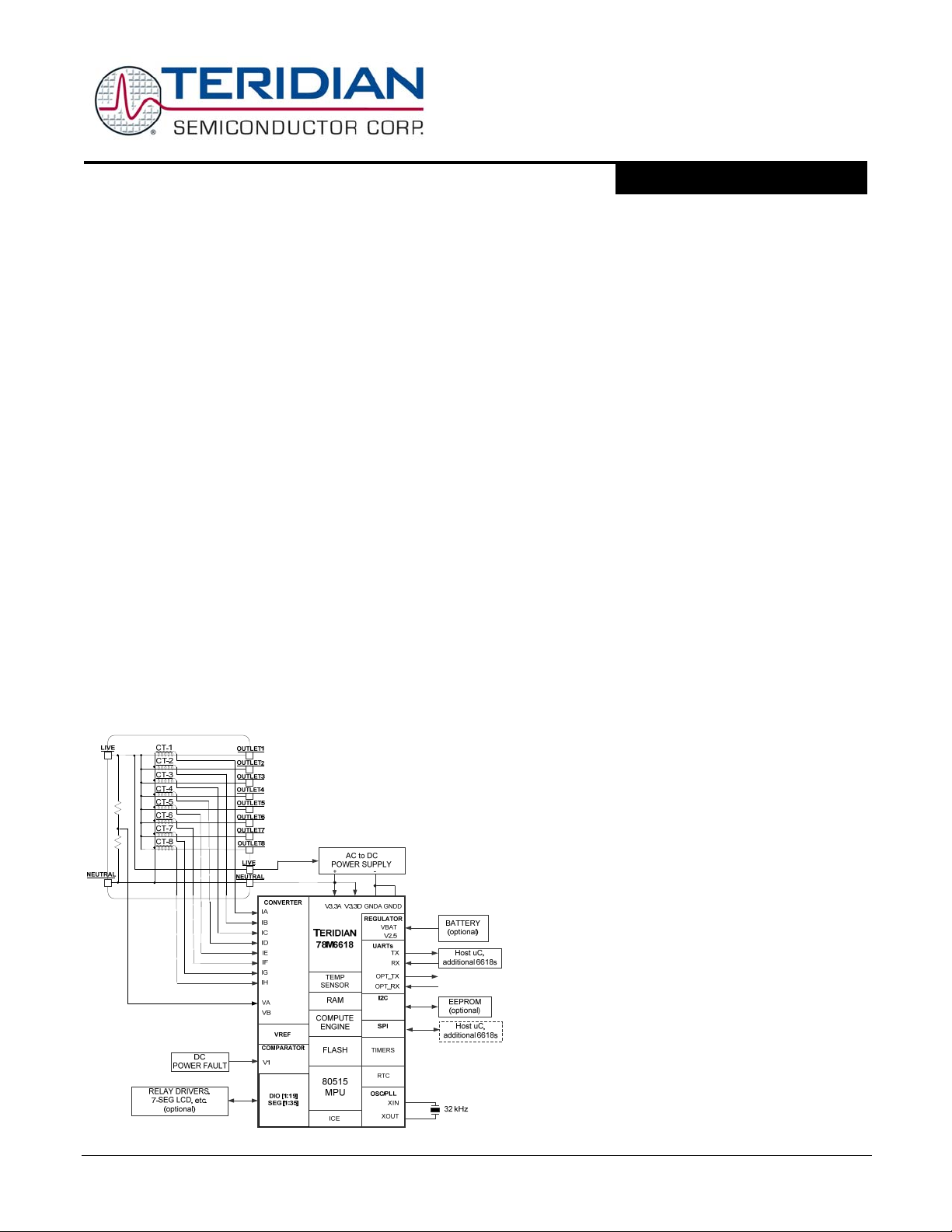
1 Hardware Functional Description
1.1 Hardware Overview
The Teridian 78M6618 single-chip measurement and monitoring IC integrates all the primary AC
measurement and control blocks required to i m plem ent an 8-outlet single-phase PDU with per outlet
metering and intelligent relay control The 78M66 18 i ncludes:
• A ten-input analog front end (AFE)
• An independent digital computation engine (CE)
• An 8051-compatible microprocessor (MPU) w hich executes one instruction per clock cycle (80515)
• A precision voltage reference
• A temperature sensor
• RAM and Flash memory
• A variety of I/O pins
• LCD drivers
Various current sensor technologies are supported including Current Transformers (CT), Resistive Shunts
and Rogowski coils.
In a sub-metering application, the 32-bit compute engine (CE) of the 78M6618 sequentially process the
samples from the analog inputs on pins IA, IB, IC, ID, IE, IF, IG, IH, VA, VB and performs calculations to
measure active energy (Wh) and reactive energy (V A Rh), as well as A
measurement. These measurements are then accessed by the MPU, processed further, and output via
the peripheral devices available to the MPU.
In addition to the temperature-trimmed ultra-precision voltage reference, the on-chip digital temperature
compensation mechanism includes a temper ature sensor and associated controls for correction of
undesirable temperature effects on measurement accuracy. Temperature-dependent external
components such as a crystal oscillator and current sensors can be characterized and their correction
factors can be programmed to produce measurements with exceptional accuracy over the industrial
temperature range.
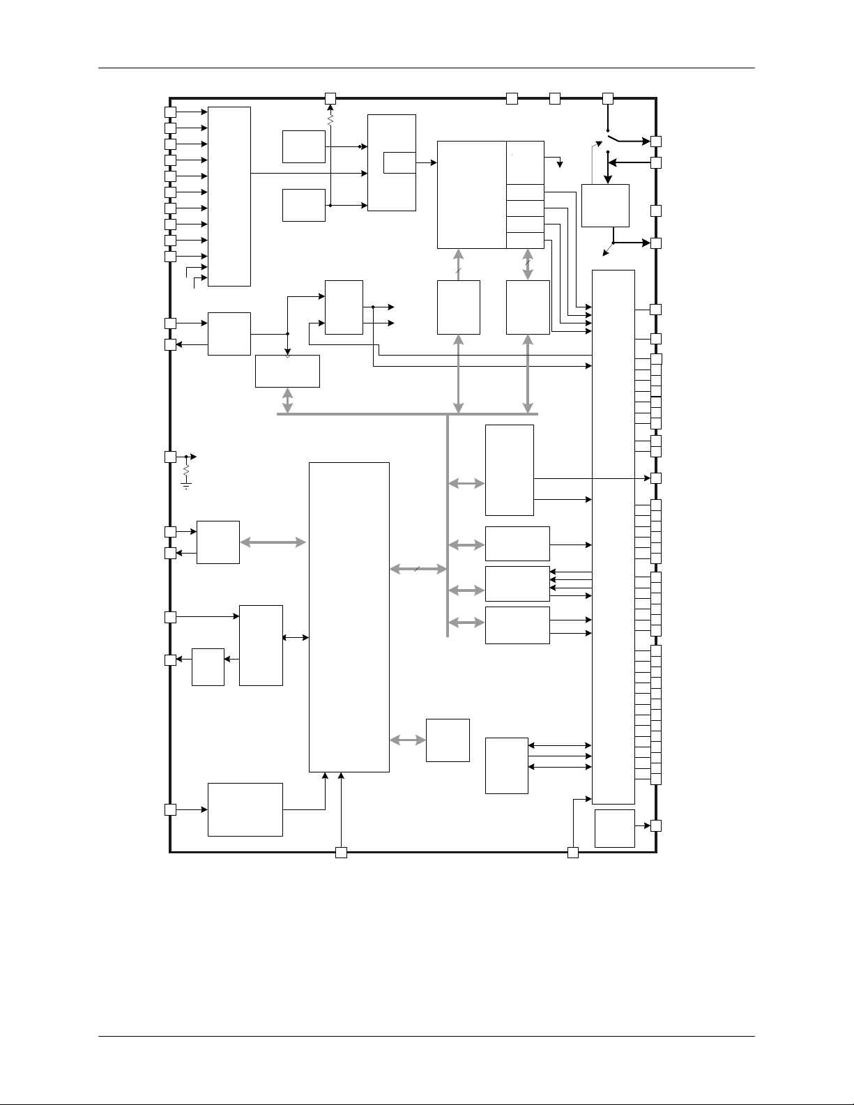
A block diagram of the 78M6618 IC is shown in Figure 1. A detailed description of the various f unct i onal
blocks follows.
2
h and V2h for four-quadrant
Rev. 1.4 5
78M6618 Data Sheet DS_6618_005
∆Σ ADC
CONVERTER
VREF
MUXP
XIN
XOUT
VREF
RESET
V1
UART
TX
RX
COM1, 0
LCD DISPLAY
DRIVER
DIGITAL I/O
POWER FAULT
GNDD
V3P3A
V3P3D
VBAT
VOLT
REG
2.5V to logic
V2P5
TMUXOUT
FAULTZ
GNDA
VBIAS
TEMP
OSC
(32.768kHz)
MCK
PLL
VREF
TEST
TEST
MODE
E_RXTX
RTC
VBIAS
ICE_E
V3P3SYS
TEST
MUX
VBAT
CE_PROG
CK_CE
CK_MPU
80MHz
VADC
CE
MULTI-
PURPOSE
IO
RTM
RPULSE
WPULSE
COM0, COM1
SEG0...
DIO_4...
to TMUX
SPI SLAVE
EEPROM I/F
FLASH
128KB
XRAM
4kB
CE_DATA
PCSZ
PCLK
PSDI
PSDO
SDATA
SCLK
SFR
80515
MPU
EMULATOR
E_TCLK
E_RSTZ
SEG7
SEG8
SEG9 / E_RXTX
SEG10 / E_TCLK
SEG11 / E_RST
SEG12
SEG14
SEG16
SEG15
SEG17
DIO4 / SEG24
DIO5 / SEG25
DIO6 / SEG26
DIO7 / SEG27
DIO10 / SEG30
RPULSE
WPULSE
XRAM BUS
8
16
32
CKTEST
ICE_E
CKTESTI
SEG0
SEG1
SEG2
SEG3 / PCLK
SEG4 / PSDO
SEG5 / PCSZ
SEG6 / PSDI
FIR
IH
VA
VB
IG
XPULSE
YPULSE
XPULSE
YPULSE
DIO8 / SEG28
DIO9 / SEG29
SEG18
SEG19
DIO43 / SEG63
DIO18 / SEG38
DIO17 / SEG37
DIO13 / SEG33
DIO14 / SEG34
DIO15 / SEG35
DIO16 / SEG36
ID
IE
IF
IC
IA
IB
OPT_RX /
DIO1
OPT_TX /
DIO2
OPTICAL
MOD
DIO3
DIO11 / SEG31
DIO19 / SEG39
6 Rev. 1.4
Figure 1: 78M6618 IC Functional Block Diagram

DS_6618_005 78M6618 Data Sheet
1.2 Device Reset
When the RESET pin is pulled high, all digital activity stops. Only the oscillator and RTC module continue
to run. Additionally, all IORAM bits are set to their default states. As long as V 1 (the input voltage at the
power fault block) is greater than VBIAS , the internal 2.5 V regulator will continue to provide power t o the
digital section.
Once initiated, the reset mode will persist until the reset timer times out. This will occur in 4096 cycl es of
the crystal clock after RESET goes l ow, at which time the MPU will begin executing its preboot and boot
sequences from address 0x0000.
1.3 Power Management
1.3.1 Voltage Regulator
The 78M6618 provides an on chip voltage regulator to create a 2.5V supply for the digital logic. T his
regulator can be run off of the V3P3SYS or VBA T inputs depending upon power availability.
1.3.2 Power Fault Management
The 78M6618 includes both hardware and software c ontrolled power fault management. V1 is connected
to a comparator to monitor system power fault conditions. When the output of the comparator falls
(V1<VBIAS) the device will enter BROWNOUT mode if there is sufficient voltage on VBAT. If there is not
sufficient voltage on VBAT then the part wil l enter RESET mode.
1.3.3 BROWNOUT
In BROWNOUT mode the AFE, CE and other analog circuits are disabled leaving only the non-metering
digital circuits running. The MPU is reduced t o the crystal clock rate (32kHz). From BROWNO UT the
78M6618 SW may choose to voluntarily enter other power management modes. See the 78M6618
Programmer’s Reference Manual for more information regarding the programmability of the 78M6618
power management modes. If the overhead on VBAT is insufficient to maintain the BROWNOUT mode
then the device will attempt to enter SLEEP m ode. If power is restored the device will return to normal
(mission mode) operation once the PLL has settled.
1.3.4 SLEEP Mode
SLEEP mode provides the savings in battery current as only the Oscillator, and RTC functions are active.
As the CPU is disabled in SLEEP, the device can only wake up from SLEEP by the restoration of power
or RTC autowake.
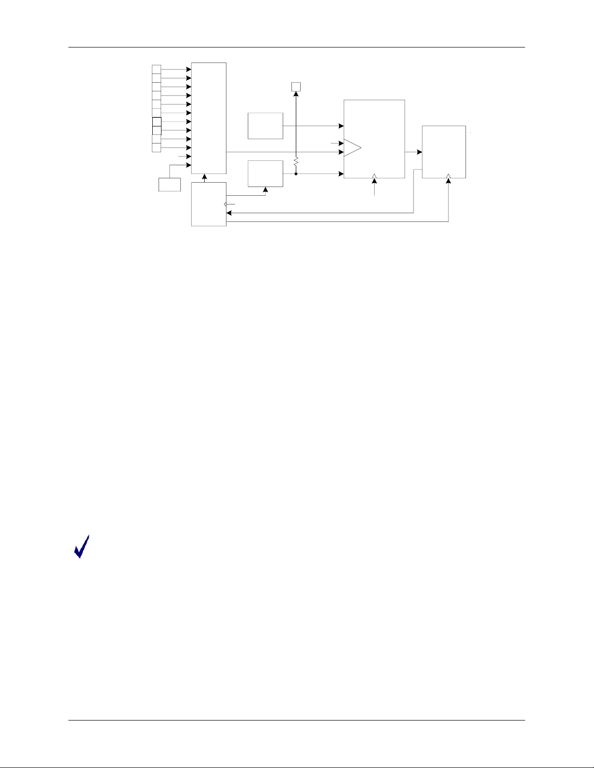
1.4 Analog Front End (AFE)
The AFE functions as a data acquisition system, controlled by the MPU. The main blocks in the AFE
consist of an input multiplexer, a del ta-sigma A/D converter, a FIR(Finite Impulse Response) filter and a
voltage reference. The metrology input si gnals (IAIH, VA, VB, VBAT and TEMP) are multiplexed before
being sampled by the ADC. The ADC output is decimated by the FIR filter and the results are stored in
XRAM where they can be accessed by the CE and th e M P U. The AFE is programmable for various
system requirements including but not limi ted to:
• Programmable Input Multiplexer settings
• Voltage reference, Battery and Temperature monitors inputs
• Programmable ADC sampling rate
• Programmable FIR length/resolution
Rev. 1.4 7
78M6618 Data Sheet DS_6618_005
IG
IH
MUX
VREF
4.9152 MHz
VBIAS
CROSS
CK32
VREF
MUX
CTRL
VA
MUX
V3P3A
FIR
VB
VBIAS
∆Σ ADC
CONVERTER
+
-
VREF
TEMP
VBAT
FIR_DONE
FIR_START
IC
ID
IE
IF
IA
IB
Figure 2: AFE Block Diagram
See the 78M6618 Programmer’s Reference Manual for more information regarding the programm ability
of the 78M6618 AFE.
1.4.1 Analog Current and Voltage Inputs
Pins IA, IB, IC, ID, IE, IF, IG, IH, VA, VB are analog inputs the AFE that provide support for measuring
current and voltage in a variety of ways. Various current sensor technologies are supported including
Current Transformers (CT), Resistive Shunt s and Rogowski coils.
1.5 Digital Computation Engine (CE)
The CE, a dedicated 32-bit digital signal processor, performs t he precision computations necessary to
accurately measure energy. Typically CE calculations and processes include:
• Scaling of the processed samples based on calibration coefficients.
• Frequency-insensitive delay cancellation on all channels
• 90° phase shifter (for narrowband VAR calculations).
• Monitoring of the input signal frequency (for frequency and phase information).
• Monitoring of the input signal amplitude (for sag detection).
• Multiplication of each voltage and current sample to obtain the energy per sample.
• RTM(Real Time Monitor) for debug purpos es
• Pulse Generators used to output CE status indicators (e.g. SAG) directly to designated DIO pins.
Due to the custom nature and complexity of the CE, generally, pre-compiled CE code is provided by
Teridian as a part of the available reference firmware and is not modified by the user. Please contact
Teridian support for more information regarding CE code.
See the 78M6618 Programmer’s Reference Manual for more information on interfacing to an d
configuration of the 78M6618 CE.
1.6 80515 MPU Core
The 78M6618 includes an 80515 MPU (8-bit, 8051-compatible) that processes most instructions in one clock
cycle. The 80515 architecture eliminates redundant bus states and implements parallel execution of fetch and
execution phases. Normally, a machine cycle is aligned with a memory fetch, therefore, most of the 1-byte
instructions are performed in a single machine cycle (MPU clock cycle). This leads to an 8x average
performance improvement (in terms of MIPS) over the Intel
See the 78M6618 Programmer’s Reference Manual for more information regarding the programm ability of
MPU Memory Organization, Special Function Registers, Interrupts, Counters, and other CPU controls.
8 Rev. 1.4
8051 device running at the same clock frequency.

DS_6618_005 78M6618 Data Sheet
1.6.1 SFR
Several custom Special Function Registers (S FR) registers are implemented in the 78M6618’s 80515
MPU. See the 78M6618 Programmer’s Reference Manual for more i nformation regarding the mapping of
functionality to specific SFR and IORAM addr esses.
1.7 XRAM
The CE and MPU share a single, general purpose 4 KB RAM (also referred to as X RA M) for data. The
XRAM is natively accessible as 32bit words fr om the CE and on 8 bit boundaries from the CPU. The
XRAM is accessed by the CPU through addresses 0x0000 to 0x0FFF.
1.8 IORAM
The MPU accesses most of its external input and output functionality as well as programmable
functionality through memory mapped IO (IORAM). The IORAM is accessed by the CPU as data
addresses 0x2000 to 0x20FF. See the 78M6618 Programmer’s Reference Manual for more information
regarding the mapping of functionality to spe cific IORAM addresses.
1.9 FLASH
The 78M6618 includes 128 KB of on-chip Flash memory. For read/write access from the CPU, the flash
is broken into four 32 KB banks that are managed by SFR settings. For erasing of the flash memory from
the CPU the flash is segmented into individual 1024-byte pages and also controlled by SFR settings. See
the 78M6618 Programmer’s Reference Manual for more information regarding the use of flash and the
mapping of functionality to specific SFR settings.
1.9.1 Program Security
The 78M6618 has functionality to guarantee t he security of the user’s MPU and CE program code. When
enabled, the security feature limits the ICE t o global Flash erase operations only. All other ICE
operations are blocked. Security is enabled by MP U code that is executed in a pre-boot interval before
the primary boot sequence begins. Once security is enabled, the only way to disable it is to perform a
global erase of the Flash, followed by a chip reset.
1.10 Oscillator
The 78M6618 oscillator drives a standard 32.768 kHz watch crystal. These crystals are accurate and do
not require a high-current oscillator circuit. The 78M6618 oscillator has been designed specifically to
handle these crystals and is compatible with their high impedance and limited power handling capability.
The oscillator is powered directly and only from the VBAT pin, which therefore must be connected to a
DC voltage source not to exceed 4 V. The oscillator requires approximately 100 nA, which is negligible
compared to the internal leakage of a batt ery
Since the oscillator is self-biasing, an external resistor must not be connected across the crystal.
1.11 PLL and Internal Clock Generation
Timing for the device is derived from the 32.768 kHz crystal oscillator output. The PLL and on-chip timing
functions provide several clocks which include:
• The MPU clock (CKMPU)
• The emulator clock (2 x CKMPU)
• The clock for the CE (CKCE)
• The delta-sigma ADC and FIR clock(CKADC, CKFIR)
These internal clocks can be adjusted for v arious programmable rates which affect device fun ct ional i ty.
See the 78M6618 Programmer’s Reference Manual for more information regarding the programmability
of the 78M6618 PLL and internal clock generation module s.
Rev. 1.4 9
 Loading...