

TERIDIAN Semiconductor 73S8024RN Technical data

73S8024RN
Low Cost Smart Card Interface
DATA SHEET
May 2010
DESCRIPTION
The Teridian 73S8024RN is a single smart card (ICC)
interface IC that can be controlled by a dedicated control
bus. The 73S8024RN has been designed to provide full
electrical compliance with ISO-7816-3, EMV 4.0
(EMV2000) and NDS specifications.
Interfacing with the system controller is done through a
control bus, composed of digital inputs to control the
interface, and one interrupt output to inform the system
controller of the card presence and faults.
The card clock can be generated by an on-chip oscillator
using an external crystal or by connection to a clock
signal.
The 73S8024RN incorporates an ISO-7816-3
activation/deactivation sequencer that controls the card
signals. Level-shifters drive the card signals with the
selected card voltage (3V or 5V), coming from an internal
Low Drop-Out (LDO) voltage regulator. This LDO
regulator is powered by a dedicated power supply input
VPC. Digital circuitry is separately powered by a digital
power supply VDD.
With its embedded LDO regulator, the 73S8024RN is a
cost effective solution for any application w here a 5V
(typically -5% +10%) power supply is available.
Hardware support for auxiliary I/O lines, C4 / C8 contacts,
is provided*.
Emergency card deactivation is initiated upon card
extraction or upon any fault generated by the protection
circuitry. The fault c an be a card over-current, a VDD
(digital power supply)**, a VPC (regulator power supply), a
VCC (card power supply) or an over-heating fault.
The card over-c urrent circuitry is a true current detection
function, as opposed to V
usually implemented in ICC interface ICs.
The VDD voltage fault has a threshold voltage that can be
adjusted with an external resistor or resistor network. It
allows automated card deactivation at a customized VDD
voltage threshold value. It can be used, for instance, to
match the system controller operating voltage range.
voltage drop detection, as
CC
APPLICATIONS
• Set-Top-Box Conditional Access and Pay-per-
View
• Point of Sales and Tra nsac tion Ter mina ls
• Control Access and Identification
* Pins/functions not available on 20-pin QFN package.
** User V
20-pin QFN package.
threshold configuration not available on
DD_FLT
ADVANTAGES
• Traditiona l step-up converter is replaced by a LDO
regulator:
Greatly reduced power dissipation
Fewer external components are required
Better noise performance
High current capability (90mA supplied to the card)
• SO28 package is pin-to-pin compatible with
industry-standard TDA8004 and TDA8024
• Card clock STOP (high and low) mode
• Small format (4x4x0.85mm) 20QFN package option
• True card over-current detection
FEATURES
• Card Interface:
Complies with ISO-7816-3, EMV 4.0 and NDS
A LDO voltage regulator provides 3V / 5V to the card
from an external power supply input
Provides at least 90mA to the card
ISO-7816-3 Activation / Deactivation sequencer with
emergency automated deactivation on card removal
or fault detected by the protection circuitry
Protection includes 3 voltage supervisors that detect
voltage drops on VCC (card), VDD (digital)**, and VPC
(regulator) power supplies
The VDD voltage supervisor threshold value can be
externally adjusted**
Over-current detection 150mA max
Card clock stop high or low*
2 card detection inputs, 1 for each possible user
polarity
Auxiliary I/O lines, for C4 / C8 contact signals*
Card CLK clock frequency up to 20MHz
• System Controller Interface:
3 Digital inputs control the card activation /
deactivation, card reset and card voltage
4 Digital inputs control the card clock (division rate
and card clock stop modes)
1 Digital output, interrupt to the syste m controller,
allows the system controller to monitor the card
presence and faults.
Crystal oscillator or host clock, up to 27MHz
• Regulator Power Supply:
4.75V to 5.5V (EMV 4.0)
4.85V to 5.5V (NDS)
• Digital Interfacing: 2.7V to 5.5V
• 6kV ESD Protection on the card interface
• Package: SO28, 20QFN or 32QFN
Rev. 1.9 © 20 09 Teridian Semicond uctor Corporation 1
73S 8024RN Dat a Sheet DS_8024RN_020
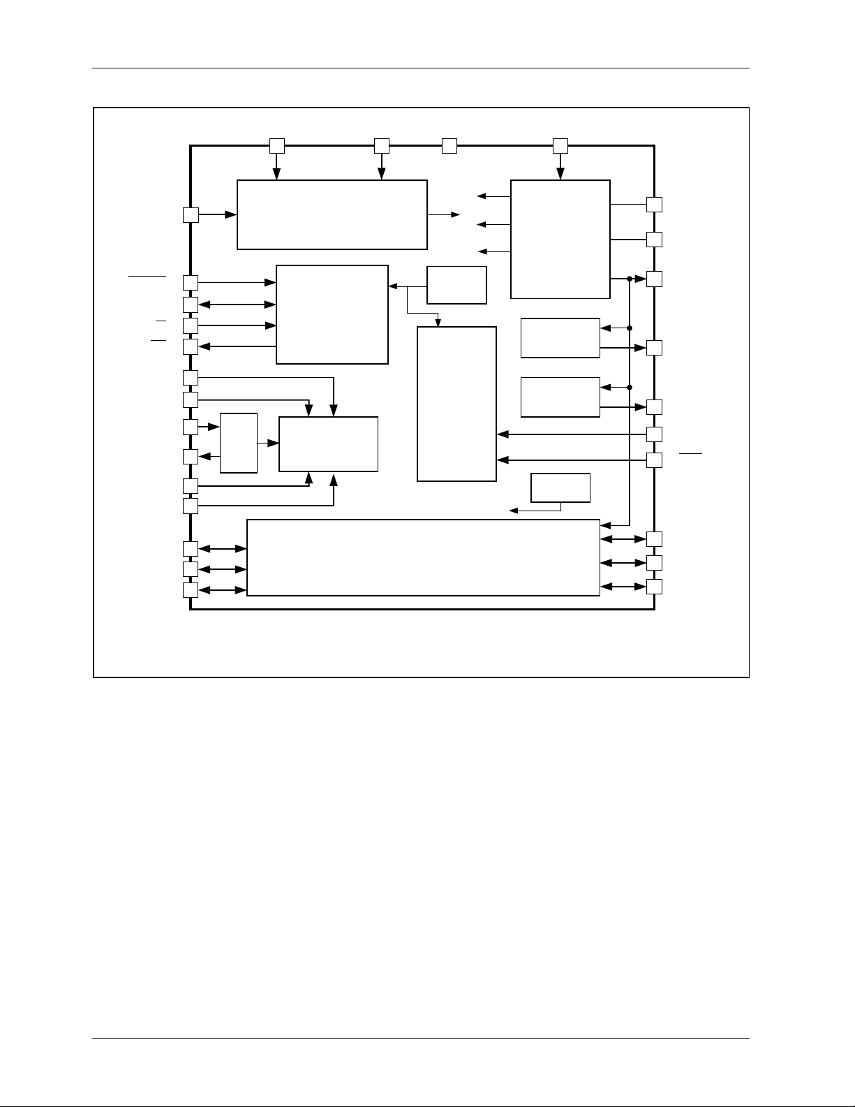
FUNCTIONAL DIAGRAM
{13} [21] 22
GND
{10} [18] 19
CMDVCC
{11} [19] 20
RSTIN
{20} [31] 3
5V/3V
{14} [22] 23
OFF
{18} [29] 1
CLKDIV1
{19} [30] 2
CLKDIV2
{15} [23] 24
XTALIN
{16} [24] 25
XTALOUT
CLKSTOP
CLKLEV
{17} [26] 26
I/OUC
AUX1UC
AUX2UC
[4] 7
[5] 8
[27]
[28]
VDD VPC
21 [20] {12}
VDDF_ADJ
18 [17]
DIGITAL POWER SUPPLY
VDD VOLTAGE SUPERVISOR
VOLTAGE REFERENCE
Int_Clk
DIGITAL
CIRCUITRY
&
FAULT LOGIC
XTAL
OSC
27
28
CLOCK
GENERATION
ICC I/O BUFFERS
NC
5 [2,9,16,25,32]
V
VDD FAULT
V
CC
I
R-C
OSC.
ISO-7816
SEQUENCER
TEMP FAULT
FAULT
PC
FAULT
FAULT
CC
6 [3] {2}
6
LDO
REGULATOR
&
VOLTAGE
SUPERVISORS
ICC RESET
BUFFER
ICC CLOCK
BUFFER
OVER
TEMP
4 [1] {1}
GND
14 [12] {6}
GND
17 [15] {9}
VCC
16 [14] {8}
RST
15 [13] {7}
CLK
10 [7] {4}
PRES
9 [6] {3}
PRES
11 [8] {5}
I/O
13 [11]
AUX1
12 [10]
AUX2
Pin numbers referen ce the 28SO package.
[Pin numbe rs] ref ere nce the 32QFN package.
{Pin numbers} reference the 20QFN package.
Figure 1: 73S8024RN Block Diagram
2 Rev. 1.9

DS_8024RN_020 73S8024RN Dat a Sheet
Table of Contents
1 Pin Description ............................................................................................................................... 5
2 System Controller Interface ........................................................................................................... 7
3 Power Supply and Voltage Supervision ........................................................................................ 8
4 Card Power Supply ........................................................................................................................ 9
5 Over-Te mp er at u re Mo nitor ............................................................................................................ 9
6 On-Chip Oscillator and Card Clock ............................................................................................... 9
7 Activation Sequence .................................................................................................................... 10
8 Deact ivation Seq uence ................................................................................................................ 12
9 OFF and Fault Detection .............................................................................................................. 13
10 I/O Circuit ry and Ti ming ............................................................................................................... 13
11 Typical Application Schematic .................................................................................................... 15
12 Electrical Specification ................................................................................................................ 16
12.1 Abs olute Maximum Rating s .................................................................................................... 16
12.2 Recommended Operating Conditions ..................................................................................... 16
12.3 Package Thermal Parameters ................................................................................................ 16
12.4 Smar t Card Interface Requir ements ........................................................................................ 17
12.5 Characteristics: Dig ital Signals................................................................................................ 19
12.6 DC Characteristics.................................................................................................................. 20
12.7 Voltage / Temperature Faul t Detecti on Circui ts ....................................................................... 20
13 Mechanical Drawing (20QFN) ...................................................................................................... 21
14 Package Pin Designation (20QFN) .............................................................................................. 22
15 Mechanical Drawing (32QFN) ...................................................................................................... 23
16 Package Pin Designation (32QFN) .............................................................................................. 24
17 Mechanical Drawing (SO)............................................................................................................. 25
18 Package Pin Designation (SO)..................................................................................................... 25
19 Ordering Information ................................................................................................................... 26
20 Related Documentation ............................................................................................................... 26
21 Contact Information ..................................................................................................................... 26
Revision History ................................................................................................................................... 27
Rev. 1.9 3

73S 8024RN Dat a Sheet DS_8024RN_020
Figures
Figure 1: 73S8024RN Block Diagram .......................................................................................................2
Figure 2: Activation Sequence – RSTIN Low When CMDVCC Goes Low
Figure 3: Activation Sequence – RST IN High When CMDVCCB Goes Low
Figure 4: Deact i vation S equence
Figure 5: Timing Diagram – Management of the Int er r upt Line OFF
Figure 6: I/O and I/OUC State Diagram
Figure 7: I/O – I/OUC Delays Timing Diagram
Figure 8: 73S8024RN – Typical Application Schematic
Figure 9: 20QFN Mechanical Drawing
Figur e 10: 20 Q FN Pi n Out
Figure 11: 32Q FN Mechan ic al Drawing
Figur e 12: 32 Q FN Pi n Out
Tables
Table 1: Choice of VCC Pin Capacit or ........................................................................................................9
Table 2: Card Clock Frequency
...............................................10
............................................11
............................................................................................................12
........................................................13
..................................................................................................14
........................................................................................14
...........................................................................15
....................................................................................................21
......................................................................................................................22
..................................................................................................23
......................................................................................................................24
................................................................................................................9
4 Rev. 1.9
Name
Pin
28SO
Pin
20QFN
Pin
32QFN
Description
I/O
11 5 8
Card I/O: Data s i gnal to/from card. I ncludes a pull-up
resistor to V
CC.
AUX1
13 – 11
AUX1: Auxiliar y data signal to/from card. In cludes a
pull-up resist or to V
CC.
AUX2
12 – 10
AUX2: Auxiliar y data signal to/from card. In cludes a
pull-up resist or to V
CC.
RST
16 8 14
Card reset: provides reset (RST) sig nal to card.
CLK
15 7 13
Card clock: pr ovides clock signal (CLK) to c ar d. The rate
frequency or frequency of the external clock signal applied
PRES
10 4 7
Card Presence s witch: active high indicates card is
Includes a high-impe da nc e pul l -down current source.
9 3 6
Card Presence switch: active low ind i cates card i s
Includes a high-impe da nc e pul l -up current source.
VCC
17 9 15
Card power supply – logically controlled by sequencer,
capacitor to the card GN D .
GND
14 6 12
Card ground.
Name
Pin
28SO
Pin
20QFN
Pin
32QFN
Description
XTALIN
24
15
23
Crystal oscillator input: can either be connected to crystal
or driven as a sou r ce for the card clock.
XTALOUT
25
16
24
Crystal oscillator output: connected t o crystal. L eft open
if XTALIN is being used as external clock input.
VDDF_ADJ
18 – 17
VDD fault threshold adjus tment input : this pin can be used
NC 5 –
2, 9,
Non-connected pin.
Name
Pin
28SO
Pin
20QFN
Pin
32QFN
Description
VDD
21
12
20
System inter fac e supply voltage and supply voltage for
internal circu itry.
VPC 6 2
3
LDO regulator power supply source.
GND 4 1
1
LDO Regulator ground.
GND
22
13
21
Digital ground .
DS_8024RN_020 73S8024RN Dat a Sheet
1 Pin Description
CARD INTERFACE
of thi s clock is determined by the extern al crystal
on XTALIN and CLKDIV selections.
present. Should be tied to GND when not used, but it
PRES
present. Sho uld be tied to VDD whe n not us e d, but it
MISCELLANEOUS INPUTS AND OUTPUTS
16, 25,
32
POWER SUPPLY AND GROUND
output of LDO r egulator. Requires an exter nal filter
to adjust the V
values ( that controls deactivation of the
DDF
card). Must be left open if unused.
Rev. 1.9 5

73S 8024RN Dat a Sheet DS_8024RN_020
Name
Pin
Pin
Pin
Description
19
10
18
Command VCC (n egative assertion): L ogic low on this pin
present.
5V
3
20
31
5 volt / 3 volt card selection: Logi c one selects 5 volts for
pin h igh (selection of 5V card) when not connected.
CLKSTOP
7 – 4
Stops the card clock signal during a card session when
CLKLVL
8 – 5
Sets the logic l evel of the card clock S TO P mode when
as an open circuit if the clock STOP m ode is not used.
CLKDIV1
1 2 18
29
Sets the divide r atio from the XTAL oscillator (o r external
1 0 XTALIN
23
14
22
Interrupt signal to the processor. Active Low - Multi-
21kΩ pull-up to V
DD.
RSTIN
20
11
19
Reset Input: This signal is the reset command t o the card.
I/OUC
26
17
26
System controller data I/O to/from th e card. Incl udes a
pull-up resist or to V
DD.
AUX1UC
27 – 27
System cont r ol ler auxiliary data I/O to/from th e card.
AUX2UC
28 – 28
System cont r ol ler auxiliary data I/ O to/from the card.
Includes a pul l-up resistor to V
DD.
MICROCONTROLLER I NTERFACE
CMDVCC
/#V
CLKDIV2
28SO
20QFN
19
32QFN
30
causes the LDO r egulator to ramp the VCC suppl y to the
card and initi ates a card ac tivation sequence, if a card is
VCC and car d interfac e, logic low selects 3 volt operation.
When the part is to be used with a sing l e card voltage,
this pin should be tied to eit her GND or V
. However, it
DD
inc l udes a high impedance pull-up resistor to default this
set high (card clock STOP m ode). Internal pull-down
resistor allo ws this pi n to be left as an open ci r cuit if the
clock STOP mode is not used.
the clock is de-activated by setting pin 7 high. Logic low
selects card S TOP l ow. Logic hig h selects card STOP
high. Interna l pul l -down resistor allows this pin to be left
clock input) to the card clock. These pins include
pull-down resistors.
CLKDIV1 CLKDIV2 CLOCK RATE
0 0 XTALIN/8
0 1 XTALIN/4
1 1 XTALIN/2
OFF
6 Rev. 1.9
function ind ic at ing fault conditions and card presence.
Open drain output configuration. It i ncludes an internal
Includes a pul l-up resistor to V
DD.

DS_8024RN_020 73S8024RN Dat a Sheet
2 System Controller Interface
Three separ ated digital inputs allow dir ect cont r ol of the car d interfac e from the host as follo ws:
• Pin CMDVCC: When low, start s an activation sequence.
• Pin RSTIN: controls the card Reset signal (when enabled by the sequencer).
• Pin 5V/#V: Defines the card voltage.
Card clock is controlled by four digital in puts:
• CLKDIV1 and CL KDIV2 define the division rate for t he clock frequency, from the input clock
frequ ency (crystal or exter nal clock).
• CLKSTOP (active high) allows card power down mode by stopping t he card clock.
• CLKLEV defines the card clock level of the card power down mode.
Interrupt output to th e host: As lon g as the card is not act i vated, the OFF pin informs the host about the
card presence only (Low = No card in the reader). When CMDVCC is set low (Card activation sequence
requested from the host ) , low level on OFF means a fault has been detected ( e.g. card rem oval during
card session, or voltage fault, or thermal / over-current fault) that automatically initiates a deactivation
sequence.
Rev. 1.9 7

73S 8024RN Dat a Sheet DS_8024RN_020
3 Power Supply and Voltage Supervision
The 73S8024RN smart card int er fac e IC incorporates a LD O voltage r egulator. The voltage output is
controlled by the digital input 5V/#V. This r egulator is able to provide either 3 V or 5V card voltage from
the power suppl y applied on the VPC pin.
Digital circuitry is powered by the power supply applied on the VDD pin. V
range to interface with t he system controller.
Three voltage supervisors constantly chec k the presence of the voltages V
deactivation sequen ce is forced upon fault of any of these v oltage su pervisors. The two voltage
supervisors for V
when the voltage V
and VCC are linked so that a fault is generated to activate a deactivation sequence
PC
becomes lower than VCC. It allows t he 73S8 024RN to oper ate at lower VPC voltage
PC
when using 3V cards only. The v oltage regulator can provide a c urrent of at least 90 m A on V
comply easily with EMV 4 .0 and NDS speci fi cations. The V
voltage supervisor thresh ol d values ar e
PC
defin ed from applicable standards (EMV and N DS). A third voltage supervisor monitors the V
It is used to initialize the ISO-7816-3 sequenc er at power-on, and to deactivate the c ar d at power-o ff or
upon fault. The voltage threshold of the V
voltag e supervisor is internally set by default to 2.3V
DD
nominal. Howe ver, it may be desirable, in s ome applications, to modify this threshold value. The pin
VDDF_ADJ (pin 18 in the SO package, pin 17 in the 32QFN package, n ot supported in the 20Q FN
package) is used to conn ect an external resistor R
value V
. The resistor value is defined as follows:
DDF
to g r ound to raise t he VDD fault voltage to another
EXT
R
EXT
= 56kΩ /(V
- 2.33)
DDF
An al ternative method (m or e accurate) of adjusting the V
fault voltage is t o use a resistive networ k of
DD
R3 from the pin to supply and R1 from the pin to ground (see applications diagram). In order to set the
new th r eshold volt age, the equivalent resistance mus t be determined. This res istance value will be
designated Kx. Kx is defined as R1/(R1+R3). Kx is calculated as:
Kx = (2.7 89 / V
) - 0.6125 where VTH is the des i r ed new threshold voltage.
TH
To determine the values of R1 and R3, use the following formulas.
R3 = 24000 / Kx R1 = R3*(Kx / (1 – Kx))
Taking the example above, wh ere a V
fault threshold voltage of 2.7V is desired, solving for Kx gives:
DD
Kx = (2.789 / 2.7) - 0.6 125 = 0.4204 6.
Solving for R3 gives: R3 = 24000 / 0.42046 = 57080.
Solving for R1 gives: R1 = 57080 * ( 0.42046 / (1 – 0.420 46) ) = 41 412.
Using standard 1 % resistor values gives R3 = 57.6KΩ and R1 = 42.4KΩ.
These values give an equivalent resistance of Kx = 0.4228, a 0.6% error.
If the 2.3V default threshold is used, this pin must be left unconnected. The 20QFN p ackage has the V
fault threshol d fixed at this defaul t value.
also defines the vol tage
DD
, VPC and VCC. A card
DD
CC
DD
that
voltage.
DD
8 Rev. 1.9
 Loading...