


73S8009CN
Combo ISO-
7816 and USB Universal
Smart Card Interface IC
Simplifying System In tegration™
DS_8009C_026 August 2009
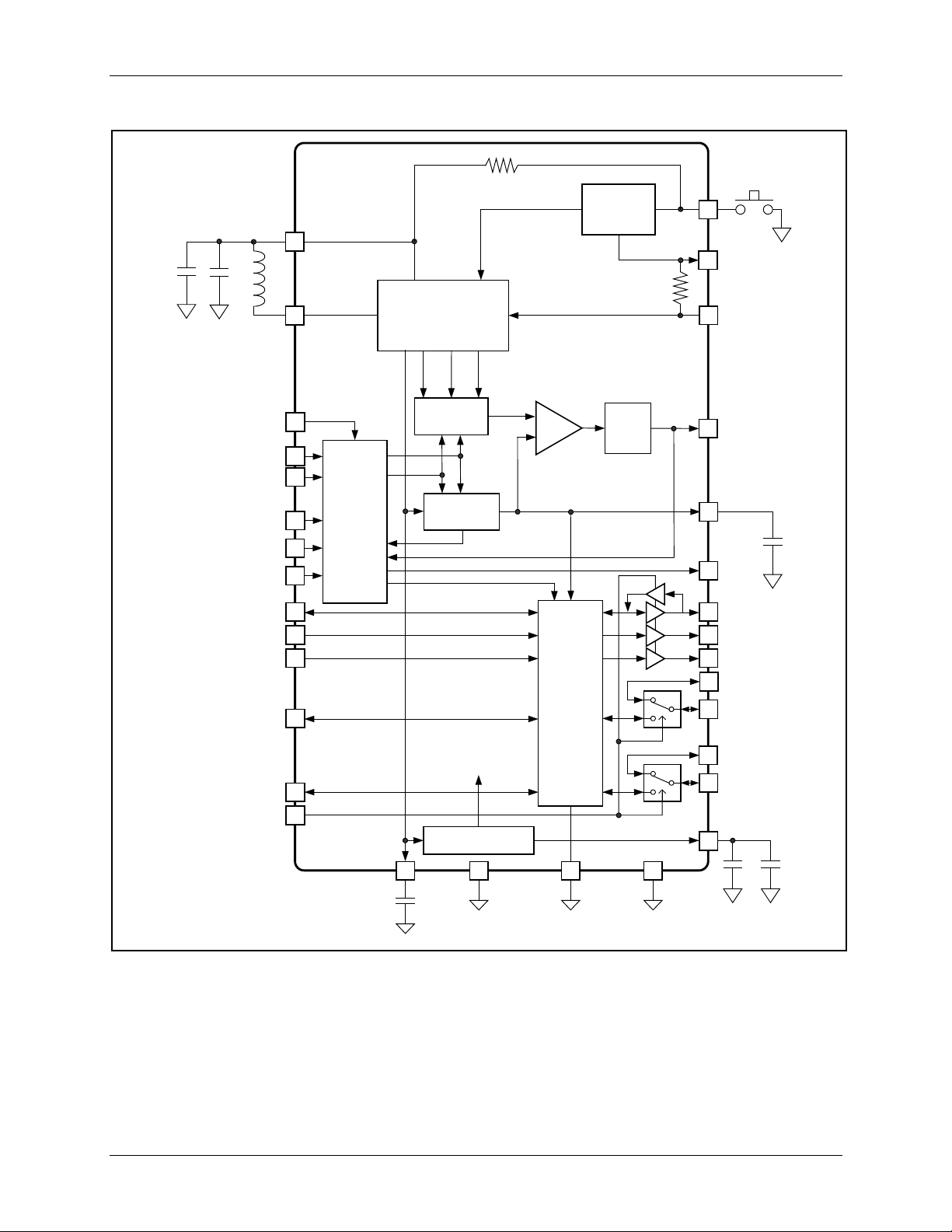
DESCRIPTION
The Teridian 73S8009CN is the world’s first
single-chip smart car d electri cal interface circuit t hat
supports al l types of smart cards: 5V, 3V and 1 .8V,
including traditional ISO-7816-3 asynchronous and
synchronous type 1 and type 2, as well as USB,
ISO-7816-12 card s.
The 73S8009CN is ideally suited for applications
such as desktop com puters, laptops and gen er al
pu r pose sm ar t card r eaders that r equire low power
operat ion fr om a single 2.7V to 6.5V power supply
voltage sou r ce. A powe r down mode (“OFF” mode)
is available and exhibi ts a 10nA typ i cal cu r r ent
consumption.
The circuit provides control, conversion and regulation
of power for the smart card. In addition, the circuit
provides a 3.3V-regul ated volt age that is u sed as an
internal dig i tal supply voltage to t he host int er face . It is
also made available to supply power to so me external
circuitry (a host cont r ol ler for instance).
For asynchronous and synch r onous sm ar t card
operat ion, the sign als for RST, C LK, I/O and auxiliary
signals AUX1 an d AUX2 ar e directly controlled from
the host pr ocessor and are level-shifted by the circuit
to the selected V
the host processor is responsible for handling the
sig nal timing for smart card activation and deactivation und er norm al conditions.
The power management circuitry allows operation
from a sing l e power suppl y source V
is converted using an inductive, step-up power
V
PC
converter t o the intermedi ate voltag e, V
by linear volt age regul ators and swit ches i nternal to
the IC to create the voltages V
. VDD is used by the 73S8009CN an d i s also
V
CC
made available for the companion host processor
circuit or for other external circuits.
The 73S8009CN features an ON/OFF pin suitable to
connect to a “push-on/push-off” main system switch.
When the 73S8009CN is “OFF,” the typical current
drawn from VPC is 10nA. For appli cations that do
not implement any ON/OFF system switch, the
ON/ OFF input pin ca n be driven from a digital output
of the host processor.
value. For more design flexibilit y,
CC
(2.7V to 6.5V).
PC
. VP is used
P
and as r equi r ed,
DD
FEATURES
• Smart Card Interface:
Smart card voltage V
o Selectable: 1.8V, 3V or 5V
o Gener ated by an in ternal voltage regulator
o Provid es up to 65m A to 3V and 5V cards
and up to 40m A to 1.8V ca r ds
ISO-7816-3 ca r d emer gency deact i vation
Volt age supervisor detects vol tage drop on
VCC (card supply)
True card over-current detection 150mA max.
1 input for a card presence detection switch
Auxiliary I/O lines for synchronous and
ISO-7816-1 2 USB card support
Proper isolation of smar t card sign al s
depending on smart card type
Card CLK clock frequency up to 20MHz
6kV ESD and short circuit protection on the
card inter face
• System Controller Interface:
Digital logic level: 3 .3V
5 si gnal images of the car d signals (RSTIN,
CLKIN, I/OUC, AUX1UC and AUX2UC)
1 control signal to switch between
synchronous / asynchronous and
ISO-7816-12 USB smart card modes
2 inputs activate and select t he card voltag e
(CMDVCC% and CMDVCC#)
2 ou tputs, interr upt t o the syst em controller
(OFF and RDY), to inform the system
controller of the card presence / faults and
status of t he inter face
1 Chip Select input
2 handshaking signals (OFF_REQ,
OFF_ACK) for proper shutdown sequencing
of all smart card signals
• ON/OFF Input for a Main System Switch
• DC-DC Step-up Converter:
Gener ates an inter mediary voltage VP
Requires a sing le 10µH In duct or ( r ated for
400mA maximum peak current)
• VDD power supply output available to power up
external circuitry: 3.3V ±0.3V, 4 0 mA
• Indust r i al temp er ature range ( -40 °C to +85 °C)
• Small form at QFN32 package: 5x5mm
• RoHS compliant (6/6) lead-free package
DATA SH EET
:
CC
Rev. 1.4 © 20 09 Teridian Semicondu ctor Corpor ation 1
73S 8009CN Data Sh eet DS_8009CN_026
V
PC
V
DD
DP
V
CC
L
IN
RDY
CMDVCC#
CMDVCC%
Delay/
Debounce
Circuit
3.3V Regulator
CS
V
CC
Regulator
Linear/
DC - DC
Converter
V1.8ThREF
V3.0ThREF
V5.0ThREF
Analog
Mux
V
P
ON
OFF
V
P
SHUTDOWN
DM
+
-
10µF
0.47µF
4.7µF
10uH
I/O
RST
CLK
AUX1
AUX2
I/OUC
RSTIN
CLKIN
AUX1UC
AUX2UC
PRES
SC/USB
GND
GND
GND
OFF
Card
I/O
Buffer
and
Signal
Logic
0.1µF
0.1µF
ON/OFF
OFF_REQ
OFF_ACK
Debounce
and Latch
100K
Card
Supply
and
Control
Logic
0.1µF
Vcc Status
TEST1
TEST2
To Internal
Digital Logic
24K
FUNCTIONAL DIAGRAM
Figure 1: 73S8009C N Block Diagram
2 Rev. 1.4

DS_8009CN_026 73S8009CN Data Sheet
Table of Contents
1 Pinout ............................................................................................................................................. 5
2 Electrical Specifications ................................................................................................................ 9
2.1 Ab solute Maximum Rati ngs ..................................................................................................... 9
2.2 Recommended Oper ating Conditions ...................................................................................... 9
2.3 Smart Card Int er face Requ i r emen ts ...................................................................................... 10
2.4 Digital Signals Characteristics ............................................................................................... 12
2.5 DC Characteristics ................................................................................................................ 13
2.6 Volt age / Tem perature Fault Detection Circuit s ...................................................................... 13
2.7 Therm al Characteri stics ........................................................................................................ 13
3 Applications Information ............................................................................................................. 13
3.1 Example 73S8009CN Schematics ......................................................................................... 13
3.2 Power Supply and Converter ................................................................................................. 16
3.3 Interface Function - ON/OFF Modes ...................................................................................... 16
3.4 System Controller Interface ................................................................................................... 18
3.5 Card Power Suppl y and V ol tage Supervision......................................................................... 18
3.6 Activation and D e-activation Sequence ................................................................................. 19
3.7 OFF and F ault D etection ....................................................................................................... 20
3.8 Chip Selection ....................................................................................................................... 21
3.9 I/O Circuitry and Timing......................................................................................................... 22
4 Equivalent Circuits ...................................................................................................................... 24
5 Mechanical Drawing .................................................................................................................... 28
6 Ordering Information ................................................................................................................... 29
7 Related Documentation ............................................................................................................... 29
8 Contact Information ..................................................................................................................... 29
Rev. 1.4 3

73S 8009CN Data Sh eet DS_8009CN_026
Figures
Figure 1: 73S8009CN Block Diag r am ...................................................................................................... 2
Figure 2: 73S8009CN 32-Pin QFN Pinout
Figure 3: Typical 73S8009CN Application Schematic with a Main System Switch
Figure 4: Typical 73S8009CN Application Schematic without a Main System Switch
Figure 5: Activation Sequence
Figure 6: D eactivation Sequence
Figure 7: OFF Activity
Figure 8: CS Timing Definitions
Figure 9: I/O and I/OUC State Diagram
Figure 10: I/O – I/OUC Delays - Timing Diag ram
Figure 11: On_Off Pin
Figure 12: Open Drai n typ e – OFF and RDY
Figure 13: Po w e r Input/Outp ut Cir cuit, VDD, LIN, VPC, VCC, VP
Figure 14: USB – DM, DP Pins
Figure 15: Smart Card CLK Driver Circuit
Figure 16: Smart Card RS T Driver Circuit
Figure 17: Smart C ar d IO , AUX1, and AUX2 Interface Circuit
Figure 18: Smart Card IOUC, AUX1UC and AUX2UC Interface Circuit
Figure 19: General Input Circuit
Figur e 20: OF F _REQ Inte r face Cir cui t
Figur e 21: 32-Pin QFN Package Dimensions
Tables
Table 1: 73S8009CN Pin Definitions ........................................................................................................ 5
Table 2: Absolu te Maximum Device R atings
Table 3: Recommended Operating Conditions
Table 4: DC S mart Card Inter face Requirements
Table 5: Digital Signals Characteristics
Table 6: DC Characteristics
Table 7: Voltage / Temperature Fault D etection Circuits
Table 8: Thermal Char acte r i stics
Table 9: Order Num bers and Packaging Marks
................................................................................................ 5
................................... 14
.............................. 15
............................................................................................................... 19
........................................................................................................... 20
............................................................................................................................ 20
.............................................................................................................. 21
.................................................................................................. 22
.................................................................................... 23
............................................................................................................................ 24
.......................................................................................... 24
........................................................... 24
.............................................................................................................. 25
.............................................................................................. 25
.............................................................................................. 25
................................................................. 26
.................................................. 26
............................................................................................................. 27
................................................................................................... 27
......................................................................................... 28
............................................................................................ 9
......................................................................................... 9
................................................................................... 10
.................................................................................................. 12
................................................................................................................... 13
......................................................................... 13
........................................................................................................... 13
...................................................................................... 29
4 Rev. 1.4
DS_8009CN_026 73S8009CN Data Sheet
6
7
8
9
5
4
3
2
1
17
18
19
20
24
23
22
21
10
11
12
13
14
15
16
32
31
30
29
28
27
26
25
LIN
VPC
RDY
PRES
I/O
ON/OFF
DM
GND
VDD
RSTIN
OFF_ACK
AUX2
AUX1
GND
CLK
RST
VCC
VP
TERIDIAN
73S8009CN
TEST1
CLKIN
DP
AUX2UC
AUX1UC
I/OUC
CS
SC/USB
CMDVCC5
CMDVCC3
OFF_REQ
TEST2
GND
OFF
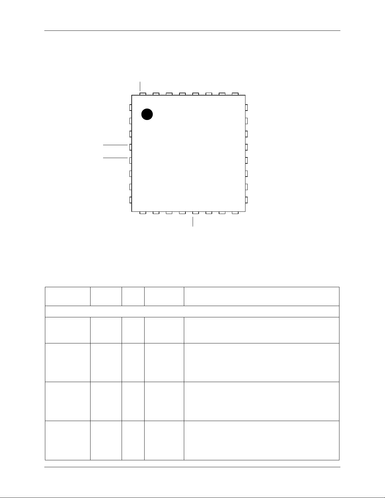
1 Pinout
The 73S8009CN is supplied as a 32-pi n QF N pa ckage.
Figure 2: 73S8 00 9C N 32-Pin QFN Pinout
Table 1 describes the pin functions for the device.
Table 1: 73S8009CN Pin Definitions
Pin
Name
Pin
Number
Type
Equivalent
Circuit
Description
Card Interface
I/O 22 IO Figure 17 Card I/O: Data signal to/from smart card. Includes
an 11kΩ pull-up resistor to V
CC
Will be tri-stated when SC/USB is set low.
AUX1 21 IO Figure 17 AUX1: Au xil iary data signal to/from smart card for
AUX2 20 IO Figure 17 AUX2: Auxiliary data signal to/from smart card for
synchronous smar t card operat ion. Smart card USB
DP signal for I S0-7816-12 U SB smart card operati on.
Includes an 11kΩ pull-up resistor to V
CC
for
synchronous / asynchronous operation only.
synchronous smar t card operat ion. Smart card USB
RST 18 O Figure 16 Card reset: provides reset (RS T) sign al to card. RST
DM signal for IS0-7816-12 US B smart card
operation. Includes an 11kΩ pull-up resistor to V
for synchronous / asynchronous oper ation only.
is the pass through signal on RSTIN. Internal con trol
logic will hold RST low when card is n ot act ivated or
VCC is too low. Will be tri-stated wh en SC/USB is
set low.
Rev. 1.4 5
CC

73S 8009CN Data Sh eet DS_8009CN_026
32
O
Figure 12
1
IO
Figure 18
2
IO
Figure 18
3
IO
Figure 18
Pin
Name
Pin
Number
Type
Equivalent
Circuit
Description
CLK 16 O Figure 15 Card clock: provides clock signal (C LK) to card. CLK
is the pass through of the signal on pi n CLKIN .
Internal con trol logic will hold CLK low when card is
not activated or VCC is too low. Will be tri-stated
when SC/USB is set low.
PRES 14 I Figure 19 S mart card Prese nce switch: Active high indi cates
card is present .
Smart card act i vation will not be permitted unless
PRES is active.
VCC 19 PSO Figure 13 Card power supply – logically control led by
sequence r , outp ut of LDO regulator. Requir es an
external 0.47uF low ES R filter ca pacitor to G N D.
GND 17 GND – Card ground.
Host Pro cesso r Interface
CS 12 I Figure 19 Chip Select. When CS = 1, the control and signal
pins are configured normally. When C S is set l ow,
CMDVCC%, RSTIN, and CMDVCC# are latched.
I/OUC, AUX1UC, and AUX2UC are set to
high-impedance pull-up mo de and do not pa ss data
to or fr om the smart card . Signals RDY and OFF are
disa bled to prevent a low outpu t and the internal
pull-up resistor s are disconnect ed. Shoul d be tied to
VDD when a single 73S8009CN is used.
OFF
Interrupt signal to th e processor. Active Low -
Multi-function indicating fault conditions and card
presence. Open drain output configuration – It
includes an internal 20kΩ pull-up to V
Pull-up i s
DD.
disabled in Power down state and CS = 0 modes.
I/OUC
AUX1UC
System controll er data I/O to/ from the card. Includes
an 11kΩ pull-up resistor to V
DD.
System controll er auxiliary data I/ O to/ from the card
for synchronous / asynchronous operation mode.
Connection to AUX1 is opened when SC/USB is low.
DD.
AUX2UC
Includes an 11kΩ pull-up resistor to V
System controll er auxiliary data I/ O to/ from the card
for synchronous / asynchronous operation mode.
Connection to AUX2 is opened when SC/USB is low.
Includes an 11kΩ pull-up resistor to V
DD.
SC/USB 13 I Figure 19 S mart Card In terface enable, USB interface disa ble.
Pin is provided with a weak pull-up.
When high, the 73S8009CN operates in
synchronous / asy nchronous operation m ode.
When low, CLK, RST I/O, AUX1, and AUX2 are
tri-stated. Pin AUX 1 is conn ected to pin DP and pin
AUX2 is connected to pin DM.
DP 25 IO Figure 14 USB D+ connection to / from USB cont r ol ler.
When SC/USB is set low, th is pin is electrically
connected to th e AUX1 pin, otherwise it is isolated.
6 Rev. 1.4
DS_8009CN_026 73S8009CN Data Sheet
6 I Figure 19
8 O Figure 12
Pin
Name
Pin
Number
Type
Equivalent
Circuit
Description
DM 23 IO Figure 14 USB D- conn ection to / from U SB con troller.
When SC/USB is set low, th is pin is electrically
connected to th e AUX1 pin, otherwise it is isolated.
CMDVCC%
CMDVCC#
4
5
I
I
Figure 19
Log i c low on on e or both of these pins will cause the
LDO regulator to ramp the Vcc supply t o the smart
card and smart car d inter face to the value described
in the following table:
CMDVCC% CMDVCC# Vcc Output Voltage
0 0 1.8V
0 1 5.0V
1 0 3.0V
1 1 Vcc Off
Note: See Card Power S upply and Voltag e
Supervision for m or e details.
RSTIN
Reset Input: This signal is the reset command to th e
card.
RDY
Signal to control l er ind i cating th e 73S8009CN is
ready because V
is above the required value aft er
CC
CMDVCC% and/or CMDVCC# is asser ted low. A
20kΩ pull-up resistor to V
is provided int ern ally.
DD
Pull-up is disabled in Power down state and CS=0
modes.
ON/OFF 24 I Figure 11 P owe r cont r ol pin . Connected to normal ly open
SPST switch to ground. Closing switch for duration
great er than de-bounce period will turn 73S8009CN
circuit “on”. If t he 73S8009CN i s “on,” closing the
switch will turn 73S8009CN to “off” state aft er the
de-bounce period and OFF_REQ/OFF_ACK
han dshake. Can be contr ol led b y a host processor
digital output.
OFF_REQ 11 O Figure 19 Digi tal output. Requ est to the host system control ler
to turn the 73S8009CN off. If ON_OFF switch is
closed (to ground) for de-bounce duration and circuit
is “on,” OFF_REQ will go high (request to turn OFF).
Connected to O FF_ACK via 100kΩ internal resi stor.
OFF_ACK 13 I Figure 19 S etting OFF_ ACK high will power “off” a ll analog
functions and disconnect the 73S8009CN from V
PC
The pin has an internal 100kΩ resistor connection to
OFF_REQ so that when not connected or n o host
interaction is requi r ed, th e Acknowledge wi l l be tr ue
and the circuit will turn “ off” after the deacti vation
sequence i s comp l eted.
Miscellaneous
.
CLKIN 7 I Figure 19 Clock signal source for the card clock.
TEST1 10 – – Fact ory test pin. This pin must be tied to GND.
TEST2 30 – – Fact ory test pin. This pin must be tied to GND.
Rev. 1.4 7
73S 8009CN Data Sh eet DS_8009CN_026
Pin
Name
Power Supply and Ground
VDD 29 PSO Figure 13 S ystem i nterface sup ply voltage output and supply
VPC 26 PSI Figure 13 Power supply source for main voltage co nverter
LIN 27 PSI Figure 13
VP 15 PSO Figure 13 In termediate output of main converter circuit.
GND 28, 31 GND – Ground.
Pin
Number
Type
Equivalent
Circuit
Description
voltage for co mpanion controller circuit (40mA
maximum so urce ca pability). R equi r es a minimum of
two 0.1µF capaci tors t o ground for proper
decoupling.
circuit. A 10µF and a 0.1µF ceramic capacit or must
be connected to this pin.
Connection to 10µH inductor for internal step up
converter. N ote: inductor mu st be rat ed for 400mA
maximum peak current.
Requires an external 4.7µF low ESR filter capacitor
to GND.
8 Rev. 1.4
DS_8009CN_026 73S8009CN Data Sheet
Parameter
Rating
Parameter
Rating
2 Electrical Specifications
This section provides the following:
Absolute maximum ratings
Recommended operating conditions
Smart card inter face requirements
Digital signals characteristics
Volt age / temperature fault d etection cir cuits
Therm al characteristics
2.1 Absolute Maximum Ratings
Table 2 l i sts the maximum operating condit ions for the 73S8009CN. Permanent device damage may
occur if absolute maxim um ratings are exceeded. Exposure to the extremes of the absol ute maximum
rating for extended p er iods may affect device reliability.
Table 2: Absolute Maximum Device Ratings
Sup ply Voltage VPC -0.5 to 7. 0 VDC
VDD -0.5 to 4. 0 VDC
Input Voltage for Di gital Inputs -0.3 to (VDD +0.5) VDC
Stor age Temperatu r e -65 to 150° C
Pin Voltag e ( except card interface) -0.3 to (VDD + 0.5) VDC
Pin Voltag e ( card interface) -0.3 to (VCC + 0.3) VDC
Pin Voltage, LIN pin 0.3 to 6.5 VDC
ESD Toleran ce – Card interface, DP and DM pins +/- 6kV
ESD Toleran ce – Other pins +/- 2kV
Pin Current, except LIN
Pin Cur r e nt, LIN + 500 mA in, -20 0 m A out
± 200 m A
2.2 Recommended Operating Conditions
Function operation should be restr icted to the r ecommended operating conditions sp ecified i n Table 3.
Table 3: Recommended Operating Conditions
Sup ply voltag e VPC 2.7 to 6.5 VDC
Ambient operating temperature -40°C to +85°C
Rev. 1.4 9

73S 8009CN Data Sh eet DS_8009CN_026
Symbol
Parameter
Condition
Min
Nom
Max
Unit
Card Power Supply (VCC) Regulator
–
–
–
–
Active mode; ICC < 40m A; 1.8V
1.68
–
1.92
V
–
–
–
Active mode; current pulses of
2.7
–
3.15
V
–
–
–
–
–
–
–
–
–
–
–
–
–
–
C
External fil ter cap for VPC
8.0
10.0
12.0
2.3 Smart Card Interface Requirements
Table 4 lists the 73S8009CN Smar t Card interface requirem ents.
Table 4: DC Smart Card Interface Requirements
General Conditions: -40C < 85C , 2. 7 V < VPC < 6.5 V
Inacti ve mode -0.1
Inactive m ode ICC = 1mA -0.1
Active mode; ICC <65 mA ; 5V 4.65
Active mode; ICC < 65mA; 3V 2.85
0.1 V
0.4 V
5.25 V
3.15 V
Active mode; single pulse of
4.6
100mA for 2 µs; 5 volt, fixed
load = 25mA
VCC
Card supp l y voltage
including ripple and noise
Active mode; single pulse of
100mA for 2 µs; 3V, fixed load
= 25mA
Active mode; current pulses of
40nAs with peak |I
CC
|
2.76
4.6
<200mA, t <400ns; 5V
40nAs with peak |ICC |
<200mA, t <400ns; 3V
Active mode; current pulses of
20nAs with peak |I
CC
|
1.62
<100mA, t <400ns; 1.8V
V
V
CCrip
I
Card supply output
CCmax
ripple f
CC
current
= 20KHz – 200MHz
RIPPLE
Static load cu r r ent, VCC>1.65
Static load cu r r ent, VCC>4.6 or
2.7 volts as se l ected
I
ICC fault current Class A, B (5V and 3V) 75
CCF
Class C (1.8V) 55
VS Vcc slew rate, r i se and
C = 0.5µF
0.10 0.30 0.70 V/μs
fall
V
V cc ready vo l tage (R DY
rdy
= 1)
5V operation, Vcc rising 4.6
3V operation, Vcc rising 2.75
1.8V operation, Vcc rising 1.65
V
RDY = 0
CCF
(V
voltag e sup er visor
CC
V
CC
= 5V
threshold)
VPC
Cvp External filter cap for VP
CF
C
VDD
External fil ter capacitor
to GND)
(V
CC
VDD filter capacitor 0.2 – 1.0
CF should be ceramic with low
ESR (<100mΩ).
2.0 4.7 6.8
0.2 0.47 1.0
5.25 V
3.15 V
5.25 V
1.92 V
350 mV
40 mA
65 mA
150 mA
130 mA
V
V
V
4.6 V
µF
µF
µF
µF
10 Rev. 1.4

DS_8009CN_026 73S8009CN Data Sheet
–
–
–
–
–
–
–
–
–
–
–
–
–
–
–
–
I
Input leakage
VIH = VCC
–
–
10
–
–
–
–
–
–
–
–
–
–
–
–
–
T
Edg e from m aster t o
60
100
200
ns
CIN
Input cap acitance
–
–
10
pF
Inusboff
Input current USB off
0 < Vdm, Vdp <3 .3V,
-2 – +2
Symbol Parameter Condition Min Nom Max Unit
Interface Requirements – Data Signals: I/O, AUX1, AUX2, and host interfaces: I/OUC, AUX1UC,
AUX2UC, DP, DM. I
SHORTL
, I
VOH Output level, high (I/O,
SHORTH
, and V
requirements do not pertain to I/OUC, AUX1UC, AUX2UC
INACT
IOH =0 0.9 * VCC
VCC+0.1 V
AUX1, AUX2)
VOH Output level, high (I/OUC,
AUX1UC, AUX2 UC)
VOL Output level, low (I/O,
AUX1, AUX2)
VOL Output level, low (I/OUC,
= -40µA
I
OH
IOH =0 0.9 VDD
= -40µA
I
OH
IOL=1mA
IOL=1mA
0.75 V
0.75 V
CC
DD
VCC+0.1 V
VDD+0.1 V
VDD+0.1 V
0.15 *VCC V
0.3 V
AUX1UC, AUX2 UC)
VIH Input level, high (I/O,
0.6 * VCC
VCC+0.30 V
AUX1, AUX2)
VIH Input level, high (I/OUC,
0.6 * VDD
VDD+0.30 V
AUX1UC, AUX2 UC)
VIL Input level, low (I/O,
-0.15
0.2 * VCC V
AUX1, AUX2)
VIL Input level, low (I/OUC,
-0.15
0.2 * VDD V
AUX1UC, AUX2 UC)
V
Output voltage when
INACT
outside of session
LEAK
Ifloat Input current Input current with
IOL = 0
IOL = 1mA
-2
0.1 V
0.3 V
µA
+2
µA
SC/USB = 0
IIL Input current, low (I/O,
VIL = 0
0.65 mA
AUX1, AUX2)
IIL Input current, low (I/OUC,
VIL = 0
0.7 mA
AUX1UC, AUX2 UC)
I
Short circuit output
SHORTL
current
I
Short circuit output
SHORTH
current
tR, tF Outp ut rise time, fall
times
For output low, sh or ted t o
through 33Ω
V
CC
For output high, shorted to
ground through 33Ω
For I/O, AUX 1, AUX 2,
= 80pF, 10% to 90%.
C
L
15 mA
15 mA
100 ns
For I/OUC, AU X1UC,
AUX2UC, CL=50Pf, 10%
to 90%.
tIR, tIF Input ri se, fall times
RPU Internal pull-up r esist or Output stable for >200ns 8 11 14
FD
Maximum data rate – – 1
MAX
Delay, I/O to I/OUC, AUX1
to AUX1UC, AUX2 to
– 15 – ns
AUX2UC,I/OUC to I/O,
AUX1UC to AUX1, AUX 2UC
to AUX2 (respectively falling
edge to falling edge and
rising edge to rising edge)
slave, measured at 50%
T
FDIO
RDIO
1
µs
kΩ
MHz
Rswitch Resistance D t o Aux 0 < Vdm, Vdp < 3.3V,
Rev. 1.4 11
VCC=5V, SC/ USB =1
VCC=5V, SC/USB =0
0.5 2 6
µA
Ω

73S 8009CN Data Sh eet DS_8009CN_026
Symbol
Parameter
Condition
Min
Nom
Max
Unit
Reset and Clock for card interface, RST, CLK
–
–
CC
–
–
–
–
–
–
–
–
–
–
–
–
–
–
D igit al I /O
(excep t fo r I/OUC, AUX1UC, AUX2UC; see
for those specifications)
–
–
–
–
–
–
–
–
–
–
–
–
–
–
–
–
–
VOH Output level, high
VOL Output level, low
V
O utput voltage when
INACT
=-200µA
I
OH
=200µA
I
OL
IOL = 0
outside of session
Ifloat Input current IOL = 1mA
Input current with SC/USB =
0, open circuited
I
I
Output current limit, RST
RST_LIM
Output current limit, CLK
CLK_LIM
tR, tF Output rise time, fall time CL = 35pF for CL K, 10% to
90%
CL = 200pF for RS T, 10% to
90%
δ
Duty cycle for CLK
=35pF, F
C
L
≤ 20MHz,
CLK
CLKIN duty cycle is 48% to
52%.
2.4 Digital Signals Characteristics
Table 5 lists the 73S8009CN digital signals characteristics.
Table 5: Digital Signals Characteristics
0.9 * V
0
-5
45
CC
VCC V
0.15
*V
V
0.1 V
0.3 V
+5
µA
30 mA
70 mA
12 ns
100 ns
55 %
Symbol Parameter Condition Min Nom Max Unit
Smart Card Interface Requirements
VIL Input L ow V ol tage -0.3
VIL
OFFACK
Input low voltage for
OFF_REQ pin = VDD -0.3
0.8 V
0.7 V
OFF_ACK pin
VIH I nput Hi gh Voltage 1.8
VOL Output Low Voltage IOL = 2mA
VOH Output High Voltage IOH = -1mA VDD - 0.45
R
Pull-up resistor; OFF, RDY 14 20 26
OUT
R
Resistor bet ween
ACK
70 100 130
VDD + 0.3 V
0.45 V
V
kΩ
kΩ
OFF_REQ and 0FF_ACK
|I
| Input Leakage Current GND < VIN < VDD –
IL1
tSL Time from CS goes high to
50
5 μA
ns
interface active
tDZ Time from CS goes low to
50
ns
interface inact ive, Hi-Z
tIS Set-up time, control
50
ns
signals to CS rising edge
tSI H old ti me, control signals
–
50 ns
from CS rising edge
tID Set-up time, control
50
ns
signals to CS fall
tDI Hold time, control signal s
50 ns
from CS fa ll
12 Rev. 1.4

DS_8009CN_026 73S8009CN Data Sheet
Symbol
Parameter
Condition
Min
Nom
Max
Unit
Vpc = 2.7V, VCC off, IDD = 0
–
1.7
–
mA
Vpc = 3.3V, VCC off, IDD = 0
–
1.1
–
mA
–
I
Card overcur r ent fau lt
80 – 150
mA
I
Card overcur r ent fau lt
VCC = 1.8V
60 – 130
mA
Symbol
Parameter
Condition
Min
Nom
Max
Unit
–
–
–
– 6 –
2.5 DC Characteristics
Table 6 lists the DC characteristics.
Table 6: DC Characteristics
VDD VDD Voltage 2.7v < VPC < 6.5v, I
VDDEXT
<
3.0 3.3 3.6 V
40mA.
Curr ent to E xternal
V
I
DDEXT
I
Supply Current
VPC
DD
Load
– – 40 mA
Vpc = 5.0V, VCC off, IDD = 0 – 0.7 – mA
OFF mode – 0.01 1 µA
2.6 Voltage / Temperature Fault Detection Circuits
Table 7 l i sts the volt age /t emp er ature fault detection circuits.
Table 7: Voltage / Temp e r at ure Fau lt Detection Circuits
Symbol Parameter Condition Min Nom Max Unit
I
DDmax
CCF
CCF1P8
VDD over-current limit 40
100 mA
2.7 Thermal Characteristics
Table 8 lists th e thermal characteristics.
Table 8: Ther mal Char acteris t i cs
Tj Junction tem perature
θ ja
Therm al Resistance,
– 125
70
°C
°C/W
Junction-to-Ambient
θ jc
Therm al Resistance,
°C/W
Junction-to-case
3 Applications Information
This se ction provid es general usage information for th e design and implementation of the 73S 8009C N .
The documents listed in Related Documentation provide mor e detailed information.
3.1 Example 73S8009CN Schematics
Figure 3 shows a typical ap plication schematic for th e i m plementati on of the 73S8009C N with a main
system switch. Figure 4 shows a typical app l ication schematic for t he implementation of the 73S8009CN
without a main system swit ch. N ote that m inor changes may occur to the reference m aterial from t ime to
time and th e r eader is encou r aged to contact Teridian for the latest i nformation.
Rev. 1.4 13

73S 8009CN Data Sh eet DS_8009_026
CLKIN_from_uC
C8
0.47µF,
OFF_ACK_from_uC
OFF_interrupt_to_uC
CLK track should be routed
far from RST, I/O, C4 and C8
NOTES:
1) VPC = 2.7V to 6.5V DC
I/OUC_to/from_uC
Card detection
switch is
normally closed
VDD
AUX1UC_to/from_uC
AUX2UC_to/from_uC
RSTIN_from_uC
Low ESR (<100mohms)
should be placed near the
SC connecter contact
CMDVCC%_from_uC
R2
20K
Smart Card Connector
1234567
8
9
10
VCC
RST
CLK
C4
GND
VPP
I/O
C8
SW-1
SW-2
CMDVCC#_from_uC
RDY_status_to_uC
C4
See NOTE 1
OFF_REQ_to_uC
0
C7
4.7µF
C6
27pF
C5
27pF
See
NOTE 2
2) Resistor footprint is included in ca se some filtering is needed on CLK
VPC
121011
131516
14
32 QFN73S80009CN
1
2
3
4
5
6
7
8
CS
TEST1
GND
VPC
CLKIN
AUX2
RDY
SC/USB
PRES
I/O
AUX1
DM
CLK
RST
VCC
TEST2
CMDVCC%
RSTIN
VDD
GND
OFF
AUX2UC
AUX1UC
I/OUC
CMDVCC#
VP
OFF_ACK
OFF_REQ
ON/OFF
DP
LIN
GND
17
18
19
20
21
23
24
22
9
282725
26
323129
30
10µF
10µH
VDD
Pushbutton Switch
SW1
VDD_supply_to_uC
See
NOTE 3
See
NOTE 3
3) Capacitors C4 and C5 are provisional and their footprints should be added for added noise rejection
if necessary.
4) Inductor must be rated for 400 mA maximum peak current.
See NOTE 4
5) VDD - 3.3V, +/- 0.3V, 40mA max. Schemati c assumes VDD supplies power to the host controller.
Requires min two 0.1µF caps to gnd)
See NOTE 5
C2
0.1F
C1
0.1F
USB D+ to/f r om_uC
USB D- to/fr om_uC
SC/USB_from_uC
6) The RDY signal is optional. A short delay before releasing RSTIN should suffice f or the RDY
signal function.
C3
0.1F
See NOTE 6
Figure 3: Typical 73S8009CN Application Schematic with a Main System Switch
14 Rev. 1.4

DS_8009CN_026 73S 8009CN Data Sh eet
CLKIN_from_uC
C7
0.47µF,
OFF_interrupt_to_uC
CLK track should be routed
far from RST, I/O, C4 and C8
NOTES:
1) VPC = 2.7V to 6.5V DC
I/OUC_to/from_uC
Card detection
switch is
normally closed
VDD
AUX1UC_to/from_uC
AUX2UC_to/from_uC
RSTIN_from_uC
Low ESR (<100mohms)
should be placed near the
SC connecter contact
CMDVCC%_from_uC
R2
20K
Smart Card Connector
1
2
3
4
5
6
7
8
9
10
VCC
RST
CLK
C4
GND
VPP
I/O
C8
SW-1
SW-2
CMDVCC#_from_uC
RDY_status_to_uC
C3
See NOTE 1
0
C2
4.7µF
C6
27pF
C5
27pF
See
NOTE 2
2) Resistor footprint is included in ca se some filtering is needed on CLK
VPC
121011
131516
14
32 QFN73S80009CN
1
2
3
4
5
6
7
8
CS
TEST1
GND
VPC
CLKIN
AUX2
RDY
SC/USB
PRES
I/O
AUX1
DM
CLK
RST
VCC
TEST2
CMDVCC%
RSTIN
VDD
GND
OFF
AUX2UC
AUX1UC
I/OUC
CMDVCC#
VP
OFF_ACK
OFF_REQ
ON/OFF
DP
LIN
GND
17
18
19
20
21
23
24
22
9
282725
26
323129
30
10µF
10µH
VDD
VDD_monitor_to_uC
See
NOTE 3
See
NOTE 3
3) Capacitors C5 and C6 are provisional and their footprints should be added for added noise rejection
if necessary.
4) Inductor must be rated for 400 mA maximum peak current.
See NOTE 4
5) VDD - 3.3V, +/- 0.3V, 40mA max. Schematic assumes VDD is monitored by t he host co ntroller.
Requires min two 0.1µF caps to gnd)
See NOTE 5
C2
0.1F
C1
0.1F
USB D+ to/f r om_uC
USB D- to/fr om_uC
SC/USB_from_uC
ON/OFF_Control_from_uC
0
10K
47K
47K
47K
6) Resistors are necessary to provide isolation between powered host and "OFF" 73S8009CN. Signals
should be driven low in this condition.
See NOTE 6
7) The RDY signal is optional. A short delay before releasing RSTIN should suffice for the RDY
signal function.
See NOTE 7
C4
0.1F
Rev. 1.4 15
Figure 4: Typical 73S8009CN Application Schematic without a Main System Switch

73S 8009CN Data Sh eet DS_8009CN_001
3.2 Power Supply and Converter
The 73S8009CN power supply and converter circuitry takes power from the V
supplied to V
pin i s converted to the volt age VP ut ilizing an inductive, step-up converter. A seri es power
PC
input pin. The power
PC
inductor ( nominal value = 10µH) is connected from pin VPC to pin LIN, and a 10µF and a 0.1µF filter
capacitor must be conn ected to V
. Note: When the VPC input voltage exceeds t he nomi nal VP voltage
PC
(approximately 5 .5V), the swi tch i ng operation of the converter stops and the converter acts as a pass
thr ough for V
to VP. Switchi ng operation will au tomatically resu me when VPC falls below the nomi nal VP
PC
voltage.
VP requires a 4.7µF filter capacitor and will have a nominal value of 5.5 volts duri ng normal operation. VP
is u sed by the smart card interfac e circuits ( C LK, RST, I/O , AUX1, and AUX2 ) and is the sour ce of the
. V
regulated smar t card suppl y V
CC
can be selected for values of 5V, 3V, and 1.8V.
CC
The power supply output VDD is also produced from VP. VDD is used by the 73S8009CN circuit for logic,
input / output buffering with the host. In addition, V
can be used as a 3.3V regulated power supply for
DD
some external circu itr y provided that no more than 40mA i s needed (simultaneousl y to the 65mA current
drawn from V
CC
).
3.3 Interf ac e Fun cti on - ON/OFF Modes
A power ON/OFF function is provided such that the circuit will be inoperative during the “OFF” state,
consuming minimum current from V
Option 1: 73S8009CN supplies host/system power controlled by push button ON/OFF switch:
Refer to Figure 3 for a typical electrica l schemat i c when using an ON/ OFF system switch.
The ON/OFF pin shal l be connected to an SPST switch to ground. If the circuit is OFF and the switch is
closed for a de-bounce p er iod of approxim ately 100ms, the circui t shall go into the “ON” state wh er ein al l
functions are oper ating in nor mal fashion. If the circu it is in the “ON” state and the ON/OFF pin is
connected to ground for a period greater than th e de-bounce period , OFF_REQ will be asserted high and
held regardless of the state of ON/OF F. Typical ly, the OFF_REQ signal is prese nted to a host control ler
that will assert OFF_ACK high when it has com pleted all shutdown activities. When OFF_ACK is set
high, the circuit will de-activate the smart card interface if required and turn off all analog functions and
the V
suppl y for the logic an d companion circu its. The OFF_A C K pin is connected internally to
DD
OFF_REQ wit h a resistor such that if OFF_ACK is unconnected, th e action of OFF_REQ will asser t
OFF_ACK hi gh. In t his con figuration, the ci r cuit shall go into the “OFF” state immediately if the interface
is d eactivated or immediately a fter deacti vation if previously activated.. Th e default state upon application
of power to V
is th e “ OFF”. Note th at at an y time, the controller may ass er t OFF_ACK and the
PC
73S 8009CN will go into t he “OFF” state ( r egardless of activity on the ON/OFF mai n sy stem switch).
Option 2: ON/OFF status driven fr om the host pr ocessor (no syst em swit ch):
Refer to Figure 4 for a typical electrica l schemat i c when contr ol ling the ON /OFF p in via h ost control.
The ON/OFF pin can be conn ected to a host digit al cont r ol signal to turn the 7 3S8009CN on or of f. The
host should monitor the V
suppl y to deter mine when th e switch debou nce t ime has been ach ieved so
DD
the 73S8009CN can switch states (ON or OFF). When the 73S8009CN is OFF, the host should drive the
ON/ OFF pin low t o init iate the turn ON proce ss. Th e signal mu st r emain low until the V
goes to 3.3V. The 73S8009CN is now ON and the ON/OFF pin should be driven back high. To turn off
the 73S8009CN, the host should drive the ON/OFF signal low until the V
73S8009CN is now OFF and the ON/OFF pins should be driven back high. See Note 6.
PC
.
suppl y voltag e
DD
suppl y goes to 0V. The
DD
16 Rev. 1.4

DS_8009CN_026 73S8009CN Data Sheet
Important Notes:
1. When the host is not powered by the VDD supply of the 73S8009CN, sp ecial care must be taken
as the host signals going to the 73S8009CN can be active when the device is powered OFF.
This can create issues such as excessive current drain on the control signals and potentially
prohibit proper turn ON of the 73S8009CN. Series resistors on the input signals (except the
ON/OFF input) are recommended to provide isolation and prevent any potential problems.
The recomm ended value of these resistors is 47 kΩ. It is also necessary for the host to set
these input signals to the low state (except for ON/OFF) when the 73S8009CN is OFF. False
activation of the card is possible if the
CMDVCC# or CMDVCC% inpu t s are l ow (with a card
inserted) when the 73S8009CN is powered ON. For this reason, the proper sequencing of the
73S8009C N is required . T he
CMDVCC# or CMDVCC% inputs must be set high immediately
before the ON/OFF input is taken low to turn on the 73S8009CN. The time between setting the
CMDVCC# or CMDVCC% inputs high and the setting of the ON/OFF input set low should be
kept to a minimum as the
CMDVCC# or CMDVCC% inputs, when set high with the 73S8009CN
OFF, will draw significant current under these conditions. The 47kΩ serie s resistors will
mitigate this current draw. However, some additional current will be drawn through the
resistors to the
CMDVCC# or CMDVCC% inputs during this time so it should be kept to a
minimum.
2. For applications where ON/OFF is controlled by the host , the OFF_REQ and OFF_A C K signals do
not need to be connect ed to the h ost. When the OFF_ACK p in is left unconnected, the 73S8009CN
will turn off proper ly by the act ion of the internal r esist or conn ection to OFF_REQ.
3. If the host is capable of selectively monitoring the I/ O line, i t can b e used in place of the V
monitor as i t is tied to the V
supply through a pull up resistor when the smart card interface is not
DD
supply
DD
activated.
4. When the 73S8009CN is powered OFF, the host will not be able to det ect a card event (card
inse r tion/removal). If thi s function is necessar y, then the host must mon itor the card co nnect or swi tch
separately.
5. For systems that do not use VDD to power the host cont r ol ler, the host int er face signals must operate
at 3.3V as the 73S8009CN digit al logic operat es off the V
the V
6. The ON/OFF pin is internally pulled up to V
supply.
PC
through a 24 kΩ resistor. Special care must be take n if
PC
the host signal controlling the ON/O FF signal is running at a voltage dif ferent from V
case, then either the h ost control signal m ust be a maximum V
(3.3V) supply regardless of the value of
DD
. If this is the
PC
supply tolerant open drain outp ut or
PC
an external circuit should pr ovide some isolation bet we en the host contr ol signal and the ON/OFF pin.
7. For those systems that require l ow power operation or are battery op erated, t he host contr oller circuit
firmw ar e shou ld p l ace the 73S8009CN in the OFF state if no card activity is required.
Rev. 1.4 17

73S 8009CN Data Sh eet DS_8009CN_026
3.4 System Controller Interface
Five s eparate digi tal in puts and two output s allow direct control of th e card interface from the host:
Pin CS: Chip select cont r ol.
Pin CMDVCC# and/or CMDVCC%: When low, starts an activation seq uence.
Pin RSTIN: controls the card RST signal.
Pin SC/USB: Routes AUXx si gnals to AUXxUC or USB D x pins and provides proper tri-stating
functionality.
Pin RDY: Indicates when smart card power supply is stable and ready.
Pin OFF: Indicat or of card presence and any car d fault condition s.
Interrupt output to the host: When t he card is not activated, th e OFF pin informs the host about the card
presence only (Low = No card in the reader, high = card inserted). When CMDVCC (#/% signals) is/are
set low (card activa tion sequ ence requested from the host), low level on OFF means a fault has been
detected ( e.g. card removal dur ing card session, or voltage f ault, or thermal / over-current fault) that
automati cally ini tiates a deactivation sequ ence. The smart card pass through si gnals are enabl ed when
the RDY conditi ons are met.
3.5 Card Po wer Sup ply and Volt ag e Superv ision
The 73S800 9CN smart card inter face IC in corporates an LDO voltage regulator for th e card power
supply, V
input sequence of CMDVCC# and CMDVCC%. This regulator is able to provide eith er 1.8V, 3V or 5V
card voltage sourced from the V
supply (except for the ON/OFF circuitry which is powered from V
value of the voltage V
supervisor, overcurrent condition, or card removal event. The voltage regulator can provide a card
current of 65mA in compliance with EMV 4.1 for 3-V and 5-V cards. The signals CMDVCC# and
CMDVCC% co ntrol the turn-on, output voltage value, and turn-off of V
low, V
V
CC
will ram p to the sel ected value or if both sign als are asser ted low (within 400ns of each other),
CC
will ram p to 1.8V. These signals are edge triggered. If CMDVCC% is asserted low (to command VCC
to be 5V) and at a much later time (greater than 2µs, typically), CMDVCC# is asserted low, i t will be
ignored (and vice versa.)
At the assertion (low) of either or both CMDVCC (#/% signals), V
rises to an accept able value, and stays above that value for approximately 20µs, RDY will be set
V
CC
high. Appr oximately 510µs after the fall of CMDVCC (#/%), the circuit will check the see if V
above the required minimum value (indicated by RDY=1) and if not, will begin an emergency deactivation
sequence. During the 510µs time, car d rem oval, or de-assertion of CMDVCC (#/%) shall also initiate an
emergency deacti vation sequence . The circuit provides over-cur rent protecti on and limits Icc to 150mA,
maximum for se lf-protecti on. When an over-current condition is sensed, the circuit will invoke a deactivation sequence .
to VCC conversion uses an internal LDO). The voltage outp ut is controlled by the digital
CC (VP
power supply. Internal digital circuitry is also powered by th e VP power
P
). A voltage supervisor checks the
PC
. A card deactivation sequence is forced upon fault detected by voltage
CC
. Wh en either signal is asser ted
CC
will rise to the requested valu e. When
CC
is at or
CC
18 Rev. 1.4

DS_8009CN_026 73S8009CN Data Sheet
CMDVCC5 or CMDVCC3
VCC
I/OUC
I/O
RDY
RSTIN
RST
CLKIN
CLK
Ignored
Ignored
Ignored
I/O, AUX1, AUX2, CLK, RST are held LOW until RDY = 1 an d CM DV CCx = 0
I/O = I/OUC if RDY=1
CLK=CLKIN if RDY=1
RST = RSTIN if RDY=1
t1
At t1 (500us), if RDY=0 or overcurrent, circuit will de-activate (safety feature)
VCC valid
3.6 Activation and De-a ctiv ati on Se que nc e
The host controller i s fully responsible for the activation sequencing of the smart card signals CL K, RST,
I/O, AUX1 and AUX2. All these signals are held low by the 73S8009CN when the card is in the deactivated state. Upon card activation (the fall of CMDVCC (#/%)), all the signals ar e held low by the
73S8009CN until RDY goes high. The host should set the signals RSTIN, I/OUC, CLKIN, AUX1UC and
AUX2UC low prior to activating the card and al l ow RDY to go high before transi tioning any of these
sig nals. In order t o init iate activati on, the card must be present and OFF must be high.
Deactivation is initi ated either by the system controller by setti ng both CMDVCC (#/%) high, or
automati cally in the event of hardware faults or assertion of the OF F_ACK si gnal. Hardware faults ar e
over-cu r rent, under-voltage, and card extraction duri ng the se ssion . The host can manage the I/O
signals, CLKIN, RSTIN, and CMDVCC (#/%) to cr eate oth er de-acti vation sequence s for non-emergency
situations.
The following steps show the deacti vat ion sequence and the t iming of the card control signals when the
system con troller sets the CMDVCC(x)B high:
1. RST goes low at the end of time t1.
2. De-assert CLK at the end of time t2.
3. I/O goes low at the end of time t3. Exit reception mode.
4. De-assert internal VCC_ON at the end of t ime t4 . After a delay, VCC is de-asserted.
Note: Since the 73S800 9CN does not co ntrol the wavesh ape of CLK (i t is det er mined by the input form
the host CL KIN), there is no guarantee that the duty cycle of the last CLK high pulse will co nform to duty
cycle requirements during an emergency deactivation.
Figure 5: Activation Sequence
Rev. 1.4 19

73S 8009CN Data Sh eet DS_8009CN_026
CMDVCC
RST
CLK
I/O
VCC_ON
VCC
t1 t2 t3
t4
t5
PRES
OFF
CMDVCC
VCC
outside card session within card session
OFF is low by
card extracted
OFF is low by
any fault
within card
session
Figure 6: Deact ivatio n Sequence
3.7 OFF and Fault Detection
There ar e two di fferent case s th at the system cont r ol ler can monitor the OFF signal: to query regarding
the card presen ce out side card sessi ons, or for fault detection durin g card se ssion s.
Outside a car d session: In thi s condi tion, CMDVCC (#/%) are al w ays hi gh, OFF is l ow if th e card is not
present, and h ig h if the card is p r esent . Because it is outside a card session, no fault detection can occu r
and it will not act upon the OFF signal. N o deact i vation is required durin g this t ime.
Duri ng a ca r d session: CMDVCC# and/or CMDVCC% is always low, and OFF falls low if the card is
extracted or i f any fault detection is dete cte d. At the sa me time that OFF is set low, the sequence r starts
the deact i vation process and the host shou l d stop al l tran sitions on the signal lines.
Figure 4 shows the timing diagram for the signals CMDVCC (#/%), PRES, and OFF during a card session
and outside the card session.
Figure 7: OFF Activity
20 Rev. 1.4
DS_8009CN_026 73S8009CN Data Sheet
CS
OFF, I/OUC,
AUX1UC, AUX2UC
CONTROL SIGNALS
FUNCTIONAL
HI-Z STATE
HI-Z STATE
t
SL
t
DZ
t
IS
t
SI
t
ID
t
DI
3.8 Chip Sel ect ion
The CS pin allows multiple cir cuits to operate in parallel, driven from th e same host cont r ol bus. When
CS is high, the pins RSTIN, CMDVCC%, CMDVCC# and CLKIN control the chip as described. The pins
I/OUC, AUX1UC, and AUX2UC have 11kΩ pull-up resistors and operate to transf er data to t he smart card
via I/O, AU X1, and AUX2 when the smar t card is activated. The signals OFF and RDY have 20kΩ pull-up
resistors.
When CS goes l ow, the states of the pins RS TI N , CMDVCC%, CMDVCC, an d C LKIN are lat ched and hel d
internally. The pull-up for pins I/OUC, AUX1UC, and AUX2UC become a very weak pull-up of
app r oximately 3 microamperes. No t r ansfer of d ata is possible between I/OU C, AUX1 U C, AUX2UC and
the smart-card signals I/O, AUX1, and AUX2. The signals OFF and RDY are se t to high im pedance and
the inter nal pull-up resistors of 20kΩ are disconnected. With regard to de-activation, CS does n ot affect
the operati on of th e fault sensing circuits and card sense input. CS does not affect the act ion of SC/USB.
Figure 8: CS Timing Definitions
Rev. 1.4 21

73S 8009CN Data Sh eet DS_8009CN_026
Neutral
State
I/OUC
in
I/O
reception
I/OICC
in
No
Yes
No No
No
Yes
No
Yes
I/O
&
not I/OUC
I/OUC
&
not I/O
I/OUC I/O
yesyes
3.9 I/O Circuitry and Timing
The states of the I/O, AUX1, and AUX2 pins are low after power on reset and th ey are in hi gh when the
activation sequence r turns on the I/O reception state. See the Act i vation and De-activation Seq uence
sect i on for mor e details on when the I/O reception is enabled. The states of I/OU C, AU X1UC, and
AUX2UC are high after power on reset.
Within a ca r d session and when the I/O recept i on state i s tu rn ed on, the first I/O line on whi ch a falli ng
edg e i s det ected becomes the input I/O l i ne and the oth er becomes the output I/O line. When the input
I/O line r ising edge is detected, then both I/O lines return to their neutral state. Figu r e 6 shows t he state
diagram of how the I/O and I/OU C lines are managed t o become input or output.
Figure 9: I/O an d I/OUC State D ia gram
22 Rev. 1.4

DS_8009CN_026 73S8009CN Data Sheet
I/O
I/OUC
t
I/O_HL
t
I/O_LH
t
I/OUC_HL
t
I/OUC_LH
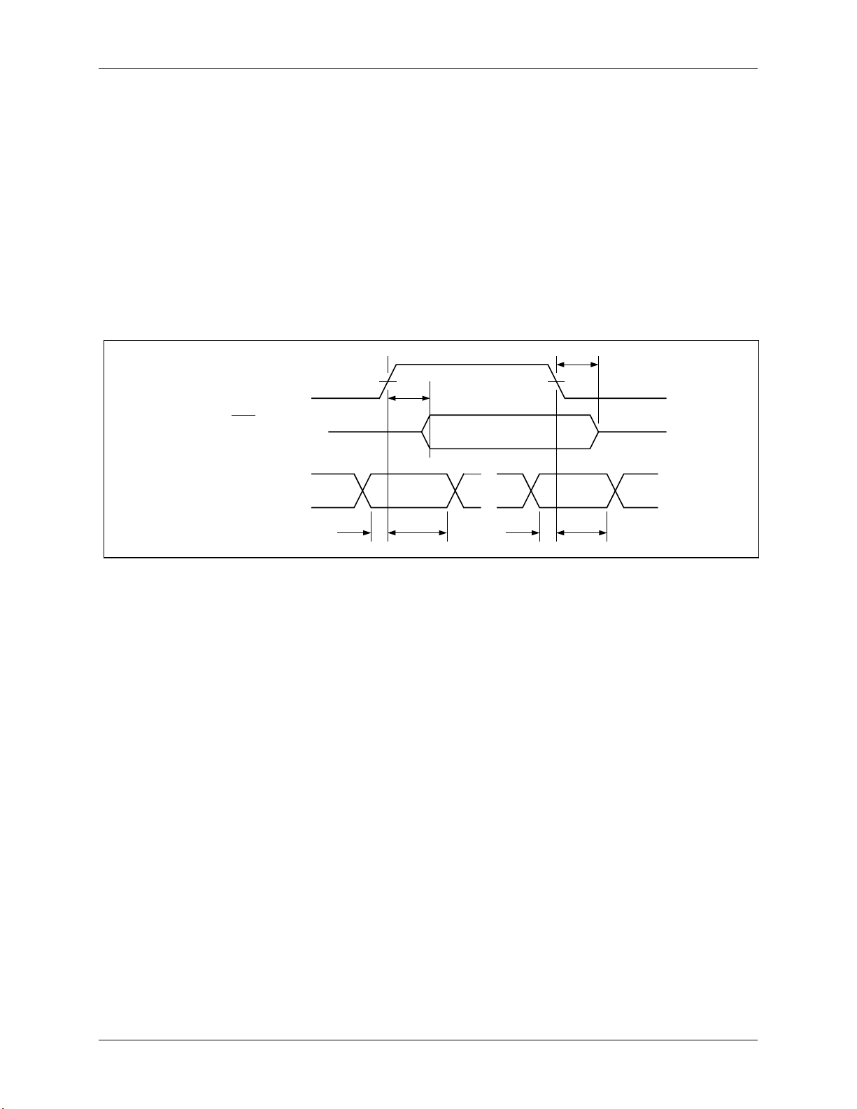
The delay between the I/O signals is shown in Figure 10.
Delay from I/O to I/OUC: t
Delay from I/OUC to I/O: t
Figure 10: I/O – I/OUC Delays - Timing Diagr a m
= 100ns t
I/O_HL
= 100ns t
I/OUC_HL
= 15ns
I/O_LH
I/OUC_LH
= 15ns
Rev. 1.4 23

73S 8009CN Data Sh eet DS_8009CN_026
PIN
ESD
VPC
24K
PIN
VDD
STRONG
NFET
Data
From
circuit
Output
Disable
20K
ESD
PIN
ESD
To
Internal
circuits
4 Equivalent Circuits
This se ction provid es illustrations of circuits equi valent to those d escribed in the Pinout section.
Figure 11: On_Off Pin
Figure 12: Open Drain type – OFF and RDY
Figure 13: Power Input/Output Circuit, VDD, LIN, VPC, VCC, VP
24 Rev. 1.4

DS_8009CN_026 73S8009CN Data Sheet
PIN
ESD
TO AUX1
or AUX2
PAD
2 ohms
CLK
PIN
VCC
VERY
STRONG
PFET
VERY
STRONG
NFET
From
circuit
ESD
ESD
RST
PIN
VCC
STRONG
PFET
STRONG
NFET
From
circuit
ESD
ESD
Figure 14: USB – DM , DP Pins
Figure 15: Smart Card CLK Driver Circuit
Figure 16: Smart Card RST Driver Circuit
Rev. 1.4 25

73S 8009CN Data Sh eet DS_8009CN_026
400ns
DELAY
IO
PIN
VCC
STRONG
PFET
STRONG
NFET
RL=11K
From
circuit
CMOS
To
circuit
ESD
ESD
400ns
DELAY
UC
PIN
VDD
STRONG
PFET
STRONG
NFET
RL=11K
From
circuit
CMOS
To
circuit
ESD
ESD
Figure 17: Smart Card IO, AUX1, and AUX2 Interface Circuit
26 Rev. 1.4
Figure 18: Smar t Card IOUC, AUX1UC and AUX2UC Interface Circuit

DS_8009CN_026 73S8009CN Data Sheet
PIN
VDD
TTL
To
circuit
Pull-up
Disable
VERY
WEAK
PFET
ESD
VERY
WEAK
NFET
Pull-down
Enable
ESD
PIN
VDD
STRONG
PFET
STRONG
NFET
Data
From
circuit
To
OFF_ACK
pad
Output
Disable
ESD
ESD
100k ohm
Note: Pins CMDVCC%, CMDVCC#, CS, SC/USB have the pull-up enabled.
Pins RSTIN, CLKIN, PRES, EXT_RST have the pull-down enabled.
Pin OFF_ACK has a 100kΩ resistor connected to pin OFF_REQ internally.
Figure 19: General Input Circuit
Notes: Strong PFET or NFET is approximately 100Ω
Very strong PFET or NFET is approximately 50Ω
Figure 20: OFF_REQ Interface Circuit
Medium strength PFET is approximately 1kΩ
Very weak PFET or NFET is approximately 1MΩ
The diodes represent ESD protection devices that will conduct current if forward biased.
Rev. 1.4 27

73S 8009CN Data Sh eet DS_8009CN_026
2.5
5
2.5
5
TOP VIEW
1
2
3
0.2 MIN.
0.35 / 0.45
1.5 / 1.875
3.0 / 3.75
0.18 / 0.3
BOTTOM VIEW
1
2
3
0.25
0.5
0.5
0.25
3.0 / 3.75
1.5 / 1.875
0.35 / 0.45
CHAMFERED
0.30
0.85 NOM./ 0.9MAX.
0.00 / 0.005
0.20 REF.
SEATING
PLANE
SIDE VIEW
5 Mechanical Drawing
Figure 21: 32-Pin QFN Package Dimensions
28 Rev. 1.4

DS_8009CN_026 73S8009CN Data Sheet
Part Description
Order Number
Packaging Mark
73S8009CN-32QFN
73S8009CN-32IMR/F
S8009CN
6 Ordering Information
Table 9 l i sts the order numbers and packaging marks used to identify 73S8009CN products.
Table 9: Order Numbers and Packaging Marks
73S8009CN-32QFN
32-pi n Le a d-Free QFN
32-pi n Le a d-Free QFN Tape / Reel
73S8009CN-32IM/F S8009CN
7 Related Documentation
The following 73S8009CN document is available from Teridian Semi conductor C or porati on:
73S8009CN 32QFN Demo Board User’s Guide
8 Contact Information
For m or e i nformation about Teridian Semicondu ctor products or to check the availability of the
73S8009CN, contact us at:
644 0 Oak Canyon Road
Suite 100
Irvin e, CA 92618-5201
Telephone: (714) 508-8800
FAX: (714) 508-8878
Email: scr.sup port@teridian.com
For a complete list of worldwide sales offic es, go to http://www.teridian.com.
Rev. 1.4 29
 Loading...