

TERIDIAN Semiconductor 73S1215F Technical data

73S1215F
80515 System-on-Chip with USB,
ISO 7816 / EMV, PINpad and More
Simplifying System Integration™
GENERAL DESCRIPTION
The 73S1215F is a versatile and economical
CMOS System-on-Chip device intended for smart
card reader applications. The circuit features an
ISO 7816 / EMV interface, an USB 2.0 interface
(full-speed 12Mbps device) and a 5x6 PINpad
interface. Maximum design flexibility is supported
with additional features such as 9 user I/Os,
multiple interrupt options, up to 4 programmable
current outputs (to drive external LEDs), and 1
analog voltage input (suitable for DC voltage
monitoring such as battery level detection). Other
built-in hardware interfaces include an
asynchronous serial UART and an I
The System-on-Chip is built around an 80515 high
performance core. Its feature and instruction set is
compatible with the industry standard 8051, while
offering one clock-cycle per instruction processing
power (most instructions)With a CPU clock running
up to 24MHz, it results in up to 20 MIPS available
that meets the requirements of various encryption
needs such as AES, DES / 3-DES and even RSA
(for PIN encryption for instance). The circuit
requires a single crystal, which frequency can be
between 6MHz and 12MHz. In addition, a 32768
Hz sub-system oscillator (optional) with an
independent real-time-clock counter enables standalone applications to access an RTC value. The
respective 73S1215F embedded memories are;
64KB Flash program memory, 2KB user XRAM
memory, and 256B IRAM memory. In addition to
these memories are independent FIFOs dedicated
to the ISO7816 UART and to the USB interface.
Overall, the 73S1215F offers a cost effective
solution to implement hand-held PINpad smart card
readers - USB connected, serial connected,
standalone or combo – as well as turnkey smart
card reader modules, USB or ExpressCard
Embedded Flash memory is in-system
programmable and lockable by means of on-silicon
fuses. This makes the Teridian 73S1215F suitable
for both development and production phases.
2
C interface.
®
type.
DATA SHEET
December 2008
Teridian Semiconductor Corporation offers with
its 73S1215F a very comprehensive set of
software libraries, including the smart card and
USB protocol layers that are pre-approved
against USB, Microsoft WHQL and EMV, as
well as a CCID reference design. Refer to the
73S12xxF Software User’s Guide for a
complete description of the Application
Programming Interface (API Libraries) and
related software modules.
A complete array of development and
programming tools, libraries and demonstration
boards enable rapid development and
certification of smart card readers that meet
most demanding smart card standards.
APPLICATIONS
• Hand-held PINpad smart card readers:
o Connected through USB, serial or
un-connected
o CCID-compliant
• E-banking (MasterCard CAP, etc)
• Smart card reader modules for PC laptops
and desktops: ExpressCard® , USB
• Digital Identification (Secure Login, Gov’t ID, ...)
• General purpose smart card readers
ADVANTAGES
• The ideal balance of cost and features for
high volume, USB-connected PINpad type
of applications:
o Larger built-in Flash / RAM than its
competitors
o Higher performance CPU core
o Powerful In-Circuit- Emulation and
Programming
o A complete set of ready-to-use EMV4.1 /
USB / CCID libraries
Rev. 1.4 © 2008 Teridian Semiconductor Corporation 1

73S1215F Data Sheet DS_1215F_003
FEATURES
80515 Core:
• 1 clock cycle per instruction (most instructions)
• CPU clocked up to 24MHz
• 64kB Flash memory with security
• 2kB XRAM (User Data Memory)
• 256 byte IRAM
• Hardware watchdog timer
Oscillators:
• Single low-cost 6MHz to 12MHz crystal
• Optional 32768 Hz crystal (with internal RTC)
• An Internal PLL provides all the necessary
clocks to each block of the system
Interrupts:
• Standard 80C515 4-priority level structure
• Nine different sources of interrupt to the core
Power Down Modes:
• 2 standard 80C515 Power Down and IDLE
modes
• Extensive device power down mode
Timers:
• Two standard 80C52 timers T0 and T1
• One 16-bit timer that can generate RTC
interrupts from the 32kHz clock
Built-in ISO-7816 Card Interface:
• LDO regulator produces VCC for the card
(1.8V, 3V or 5V)
• Full compliance with EMV 4.1
• Activation/Deactivation sequencers
• Auxiliary I/O lines (C4-C8 signals)
• 6kV ESD protection on all interface pins
Communication Interfaces:
• Full-duplex serial interface (1200 to
115kbps UART)
• USB 2.0 Full Speed 12Mbps Interface,
PC/SC compliant with 4 Endpoints:
• Control (16B FIFO)
• Interrupt IN (32B FIFO)
• Bulk IN (128B FIFO)
• Bulk OUT (128B FIFO)
2
• I
C Master Interface (400kbps)
Man-Machine Interface and I/Os:
• 5x6 Keyboard (hardware scanning,
debouncing and scrambling)
• Nine User I/Os
• Up to 4 programmable current outputs
(LED)
Voltage Detection:
• Analog Input (detection range: 1.0V to 1.5V)
Operating Voltage:
• 2.7V to 3.6V (3V to 3.6V when USB is in use)
• 4.75 to 5.5V for smart card supply
Operating Temperature:
• -40°C to 85°C
Packages:
• 68-pin QFN
• 44-pin QFN
Software:
•
Two-level Application Programming Interface
(ANSI C-language libraries)
• USB, T=0/T=1 and EMV-compliant smart card
protocol layers
• CCID reference design and Windows® driver
Communication with Smart Cards:
• ISO 7816 UART for protocols T=0, T=1
• (2) 2-Byte FIFOs for transmit and receive
• Configured to drive multiple external Teridian
73S8010x interfaces (for multi-SAM
architectures)
2 Rev. 1.4

DS_1215F_003 73S1215F Data Sheet
Table of Contents
1 Hardware Description ......................................................................................................................... 8
1.1 Pin Description .............................................................................................................................. 8
1.2 Hardware Overview .................................................................................................................... 11
1.3 80515 MPU Core ........................................................................................................................ 11
1.3.1 80515 Overview ............................................................................................................. 11
1.3.2 Memory Organization .................................................................................................... 11
1.4 Program Security ........................................................................................................................ 16
1.5 Special Function Registers (SFRs) ............................................................................................ 18
1.5.1 Internal Data Special Function Registers (SFRs) .......................................................... 18
1.5.2 IRAM Special Function Registers (Generic 80515 SFRs) ............................................ 19
1.5.3 External Data Special Function Registers (SFRs) ........................................................ 20
1.6 Instruction Set ............................................................................................................................. 23
1.7 Peripheral Descriptions ............................................................................................................... 23
1.7.1 Oscillator and Clock Generation .................................................................................... 23
1.7.2 Power Control Modes .................................................................................................... 27
1.7.3 Interrupts ........................................................................................................................ 33
1.7.4 UART ............................................................................................................................. 40
1.7.5 Timers and Counters ..................................................................................................... 45
1.7.6 WD Timer (Software Watchdog Timer) ......................................................................... 47
1.7.7 User (USR) Ports ........................................................................................................... 50
1.7.8 Real-Time Clock with Hardware Watchdog (RTC) ........................................................ 52
1.7.9 Analog Voltage Comparator .......................................................................................... 55
1.7.10 LED Drivers ................................................................................................................... 57
1.7.11 I2C Master Interface ....................................................................................................... 58
1.7.12 Keypad Interface ............................................................................................................ 65
1.7.13 Emulator Port ................................................................................................................. 72
1.7.14 USB Interface ................................................................................................................ 72
1.7.15 Smart Card Interface Function ...................................................................................... 76
1.7.16 VDD Fault Detect Function .......................................................................................... 110
2 Typical Application Schematic ...................................................................................................... 111
3 Electrical Specification ................................................................................................................... 112
3.1 Absolute Maximum Ratings ...................................................................................................... 112
3.2 Recommended Operating Conditions ...................................................................................... 112
3.3 Digital IO Characteristics .......................................................................................................... 113
3.4 Oscillator Interface Requirements ............................................................................................ 114
3.5 DC Characteristics: Analog Input ............................................................................................. 114
3.6 USB Interface Requirements .................................................................................................... 115
3.7 Smart Card Interface Requirements ......................................................................................... 117
3.7.1 DC Characteristics ....................................................................................................... 119
3.8 Voltage / Temperature Fault Detection Circuits ....................................................................... 119
4 Equivalent Circuits ......................................................................................................................... 120
5 Package Pin Designation ............................................................................................................... 129
5.1 68-pin QFN Pinout .................................................................................................................... 129
5.2 44-pin QFN Pinout .................................................................................................................... 130
6 Packaging Information ................................................................................................................... 131
6.1 68-Pin QFN Package Outline ................................................................................................... 131
6.2 44-Pin QFN Package Outline ................................................................................................... 132
7 Ordering Information ...................................................................................................................... 133
8 Related Documentation .................................................................................................................. 133
9 Contact Information ........................................................................................................................ 133
Revision History ...................................................................................................................................... 134
Rev. 1.4 3

73S1215F Data Sheet DS_1215F_003
Figures
Figure 1: IC Functional Block Diagram ......................................................................................................... 7
Figure 2: Memory Map ................................................................................................................................ 15
Figure 3: Clock Generation and Control Circuits ........................................................................................ 24
Figure 4: Oscillator Circuit ........................................................................................................................... 26
Figure 5: Power Down Control .................................................................................................................... 27
Figure 6: Detail of Power Down Interrupt Logic .......................................................................................... 28
Figure 7: Power Down Sequencing ............................................................................................................ 28
Figure 8: External Interrupt Configuration ................................................................................................... 33
Figure 9: Real Time Clock Block Diagram .................................................................................................. 52
Figure 10: I2C Write Mode Operation .......................................................................................................... 59
Figure 11: I2C Read Operation .................................................................................................................... 60
Figure 12: Simplified Keypad Block Diagram .............................................................................................. 65
Figure 13: Keypad Interface Flow Chart .................................................................................................... 67
Figure 14: USB Block Diagram ................................................................................................................... 72
Figure 15: Smart Card Interface Block Diagram ......................................................................................... 76
Figure 16: Smart Card Interface Block Diagram ......................................................................................... 77
Figure 17: Asynchronous Activation Sequence Timing .............................................................................. 79
Figure 18: Deactivation Sequence .............................................................................................................. 80
Figure 19: Smart Card CLK and ETU Generation ...................................................................................... 81
Figure 20: Guard, Block, Wait and ATR Time Definitions ........................................................................... 82
Figure 21: Synchronous Activation ............................................................................................................. 84
Figure 22: Example of Sync Mode Operation: Generating/Reading ATR Signals ..................................... 84
Figure 23: Creation of Synchronous Clock Start/Stop Mode Start Bit in Sync Mode ................................. 85
Figure 24: Creation of Synchronous Clock Start/Stop Mode Stop Bit in Sync Mode ................................. 85
Figure 25: Operation of 9-bit Mode in Sync Mode ...................................................................................... 86
Figure 26: 73S1215F Typical Application Schematic ............................................................................... 111
Figure 27: 12 MHz Oscillator Circuit ......................................................................................................... 120
Figure 28: 32kHz Oscillator Circuit ........................................................................................................... 120
Figure 29: Digital I/O Circuit ...................................................................................................................... 121
Figure 30: Digital Output Circuit ................................................................................................................ 121
Figure 31: Digital I/O with Pull Up Circuit .................................................................................................. 122
Figure 32: Digital I/O with Pull-Down Circuit ............................................................................................. 122
Figure 33: Digital Input Circuit ................................................................................................................... 123
Figure 34: Keypad Row Circuit ................................................................................................................. 123
Figure 35: Keypad Column Circuit ............................................................................................................ 124
Figure 36: LED Circuit ............................................................................................................................... 125
Figure 37: Test and Security Pin Circuit ................................................................................................... 125
Figure 38: Analog Input Circuit .................................................................................................................. 126
Figure 39: Smart Card Output Circuit ....................................................................................................... 126
Figure 40: Smart Card I/O Circuit.............................................................................................................. 127
Figure 41: PRES Input Circuit ................................................................................................................... 127
Figure 42: PRES Input Circuit ................................................................................................................... 128
Figure 43: USB Circuit .............................................................................................................................. 128
Figure 44: 73S1215F 68 QFN Pinout ....................................................................................................... 129
Figure 45: 73S1215F 44 QFN Pinout ....................................................................................................... 130
Figure 46: 73S1215F 68 QFN Package Drawing ..................................................................................... 131
Figure 47: 73S1215F 44 QFN Package Drawing ..................................................................................... 132
4 Rev. 1.4

DS_1215F_003 73S1215F Data Sheet
Tables
Table 1: 73S1215F Pinout Description ......................................................................................................... 8
Table 2: MPU Data Memory Map ................................................................................................................ 11
Table 3: Flash Special Function Registers ................................................................................................. 13
Table 4: Internal Data Memory Map ........................................................................................................... 14
Table 5: Program Security Registers .......................................................................................................... 17
Table 6: IRAM Special Function Registers Locations ................................................................................. 18
Table 7: IRAM Special Function Registers Reset Values ........................................................................... 19
Table 8: XRAM Special Function Registers Reset Values ......................................................................... 20
Table 9: PSW Register Flags ...................................................................................................................... 22
Table 10: PSW Bit Functions ...................................................................................................................... 22
Table 11: Port Registers ............................................................................................................................. 23
Table 12: Frequencies and Mcount Values for MCLK = 96MHz ................................................................ 25
Table 13: The MCLKCtl Register ................................................................................................................ 25
Table 15: The MPUCKCtl Register ............................................................................................................. 26
Table 17: The INT5Ctl Register .................................................................................................................. 29
Table 19: The MISCtl0 Register .................................................................................................................. 29
Table 21: The MISCtl1 Register .................................................................................................................. 30
Table 23: The MCLKCtl Register ................................................................................................................ 31
Table 25: The PCON Register .................................................................................................................... 32
Table 27: The IEN0 Register ....................................................................................................................... 34
Table 29: The IEN1 Register ....................................................................................................................... 35
Table 31: The IEN2 Register ....................................................................................................................... 35
Table 33: The TCON Register .................................................................................................................... 36
Table 35: The T2CON Register .................................................................................................................. 36
Table 37: The IRCON Register ................................................................................................................... 37
Table 39: External MPU Interrupts .............................................................................................................. 37
Table 40: Control Bits for External Interrupts .............................................................................................. 38
Table 41: Priority Level Groups ................................................................................................................... 38
Table 42: The IP0 Register ......................................................................................................................... 38
Table 43: The IP1 Register ......................................................................................................................... 39
Table 44: Priority Levels .............................................................................................................................. 39
Table 45: Interrupt Polling Sequence .......................................................................................................... 39
Table 46: Interrupt Vectors .......................................................................................................................... 39
Table 47: UART Modes ............................................................................................................................... 40
Table 48: Baud Rate Generation ................................................................................................................ 40
Table 49: The PCON Register .................................................................................................................... 41
Table 51: The BRCON Register ................................................................................................................. 41
Table 53: The MISCtl0 Register .................................................................................................................. 42
Table 55: The S0CON Register .................................................................................................................. 43
Table 57: The S1CON Register .................................................................................................................. 44
Table 59: The TMOD Register .................................................................................................................... 45
Table 61: Timers/Counters Mode Description ............................................................................................ 46
Table 62: The TCON Register .................................................................................................................... 47
Table 64: The IEN0 Register ....................................................................................................................... 48
Table 66: The IEN1 Register ....................................................................................................................... 48
Table 68: The IP0 Register ......................................................................................................................... 49
Table 70: The WDTREL Register ............................................................................................................... 49
Table 72: Direction Registers and Internal Resources for DIO Pin Groups ............................................... 50
Table 73: UDIR Control Bit .......................................................................................................................... 50
Table 74: Selectable Controls Using the UxIS Bits ..................................................................................... 50
Table 75: The USRIntCtl1 Register ............................................................................................................ 51
Table 76: The USRIntCtl2 Register ............................................................................................................ 51
Table 77: The USRIntCtl3 Register ............................................................................................................ 51
Table 78: The USRIntCtl4 Register ............................................................................................................ 51
Table 79: The RTCCtl Register ................................................................................................................... 53
Table 81: The 32-bit RTC Counter .............................................................................................................. 54
Table 82: The 24-bit RTC Accumulator ...................................................................................................... 54
Rev. 1.4 5

73S1215F Data Sheet DS_1215F_003
Table 83: The 24-bit RTC Trim (sign magnitude value) .............................................................................. 54
Table 84: The INT5Ctl Register .................................................................................................................. 54
Table 86: The ACOMP Register ................................................................................................................. 55
Table 88: The INT6Ctl Register .................................................................................................................. 56
Table 90: The LEDCtl Register ................................................................................................................... 57
Table 92: The DAR Register ....................................................................................................................... 61
Table 94: The WDR Register ...................................................................................................................... 61
Table 96: The SWDR Register.................................................................................................................... 62
Table 98: The RDR Register ....................................................................................................................... 62
Table 100: The SRDR Register .................................................................................................................. 63
Table 102: The CSR Register ..................................................................................................................... 63
Table 104: The INT6Ctl Register ................................................................................................................ 64
Table 106: The KCOL Register ................................................................................................................... 68
Table 108: The KROW Register ................................................................................................................. 68
Table 110: The KSCAN Register ................................................................................................................ 69
Table 112: The KSTAT Register ................................................................................................................. 69
Table 114: The KSIZE Register .................................................................................................................. 70
Table 116: The KORDERL Register ........................................................................................................... 70
Table 117: The KORDERH Register .......................................................................................................... 71
Table 120: The INT5Ctl Register ................................................................................................................ 71
Table 122: The MISCtl1 Register ................................................................................................................ 74
Table 124: The CKCON Register ............................................................................................................... 75
Table 126: The SCSel Register .................................................................................................................. 87
Table 127: The SCSel Bit Functions ........................................................................................................... 87
Table 128: The SCInt Register .................................................................................................................... 88
Table 130: The SCIE Register .................................................................................................................... 89
Table 132: The VccCtl Register .................................................................................................................. 90
Table 134: The VccTmr Register ................................................................................................................ 91
Table 138: The STXCtl Register ................................................................................................................. 93
Table 140: The STXData Register .............................................................................................................. 94
Table 142: The SRXCtl Register ................................................................................................................. 94
Table 144: The SRXData Register ............................................................................................................. 95
Table 146: The SCCtl Register ................................................................................................................... 96
Table 148: The SCECtl Register ................................................................................................................. 97
Table 150: The SCDIR Register ................................................................................................................. 98
Table 152: The SPrtcol Register ................................................................................................................. 99
Table 154: The SCCLK Register .............................................................................................................. 100
Table 156: The SCECLK Register ............................................................................................................ 100
Table 158: The SParCtl Register .............................................................................................................. 101
Table 160: The SByteCtl Register............................................................................................................. 102
Table 161: The SByteCtl Bit Functions ..................................................................................................... 102
Table 162: The FDReg Register ............................................................................................................... 103
Table 163: Divider Ratios Provided by the ETU Counter ......................................................................... 103
Table 164: Divider Values for the ETU Clock ........................................................................................... 104
Table 165: The FDReg Bit Functions ........................................................................................................ 104
Table 166: The CRCMsB Register ........................................................................................................... 105
Table 167: The CRCLsB Register ............................................................................................................ 105
Table 168: The BGT Register ................................................................................................................... 106
Table 170: The EGT Register ................................................................................................................... 106
Table 172: The BWTB0 Register .............................................................................................................. 107
Table 173: The BWTB1 Register .............................................................................................................. 107
Table 174: The BWTB2 Register .............................................................................................................. 107
Table 175: The BWTB3 Register .............................................................................................................. 107
Table 176: The CWTB0 Register .............................................................................................................. 107
Table 177: The CWTB1 Register .............................................................................................................. 107
Table 178: The ATRLsB Register ............................................................................................................. 108
Table 179: The ATRMsB Register ............................................................................................................ 108
Table 180: The STSTO Register............................................................................................................... 108
6 Rev. 1.4
DS_1215F_003 73S1215F Data Sheet
Table 181: The RLength Register ............................................................................................................. 108
Table 182: Smart Card SFR Table ........................................................................................................... 109
Table 183: The VDDFCtl Register ............................................................................................................ 110
Table 185: Order Numbers and Packaging Marks ................................................................................... 133
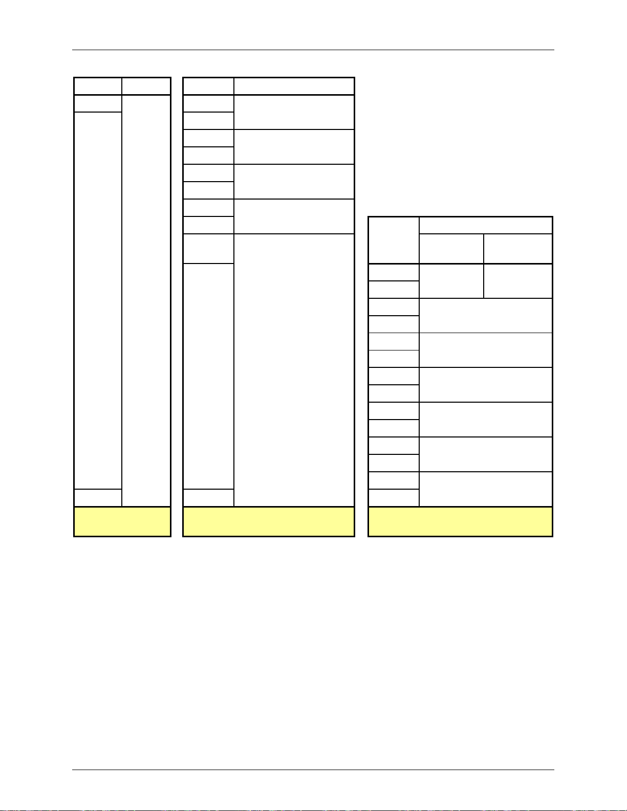
VDD
CPUCLK
X12IN
X12OUT
X32IN
X32OUT
VDD
D+
D-
GND
ROW0
ROW1
ROW2
ROW3
ROW4
ROW5
COL0
COL1
COL2
COL3
COL4
USR0
USR1
USR2
USR3
USR4
USR5
USR6
USR7
USR8
GND
TEST
PLL
and
TIMEBASES
12MHz
OSCILLATOR
32kHz
OSCILLATOR
RTC
USB I/O
and
LOGIC
KEYPAD
INTERFACE
DRIVERS
USR(8:0)
SEC
RESET
VOLTAGE REFERENCE
AND FUSE TRIM
CIRCUITRY
VPD REGULATOR
FLASH/ROM
PROGRAM
MEMORY
64KB
FLASH
INTERFACE
DATA
XRAM
2KB
VDD
ANA_IN
TCLK
MEMORY_
CONTROL
CONTROL
SCRATCH
CORE
PORTS
SERIAL
RXTX
ERST
ISBR
ICE INTERFACE
OCDSI
RAM_
SFR_
IRAM
256B
ALU
PMU
PERIPHERAL
INTERFACE
and SFR LOGIC
TBUS2
TBUS3
CONTROL
UNIT
TIMER_0_
1
WATCH-
DOG
TIMER
ISR
TBUS1
TBUS0
CONTROL
SMART CARD LOGIC
ISO UART and CLOCK GENERATOR
LED
DRIVERS
VPC
VCC
LOGIC
SMART
CARD
ISO
INTERFACE
EXTERNAL
SMART
CARD
INTERFACE
MASTER
I
INT.
VCC
GND
RST
CLK
I/O
AUX1
AUX2
PRES
PRESB
SCLK
SIO
INT2
INT3
2
C
SCL
SDA
Pins avaiable on both 68 and 44 pin packages.
Pins only avaiable on 68 pin package.
GND
TXD
RXD
LED1
LED2
LED0
LED3
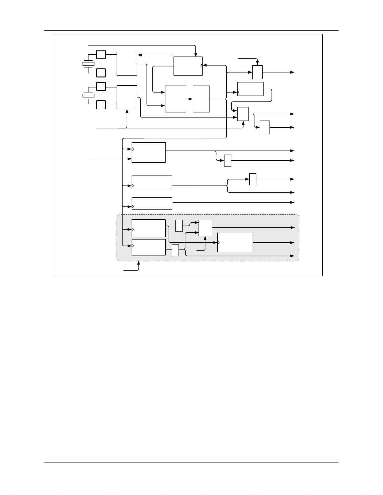
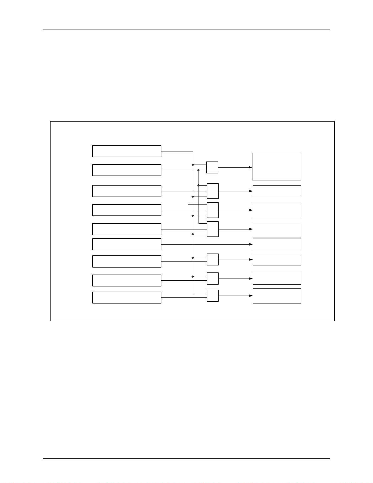
Figure 1: IC Functional Block Diagram
Rev. 1.4 7
73S1215F Data Sheet DS_1215F_003
1 Hardware Description
1.1 Pin Description
Table 1: 73S1215F Pinout Description
Pin Name
Pin (68 Qfn)
Pin (44 Qfn)
Type
Equivalent
Description
Circuit*
X12IN 10 8 I Figure 27 MPU/USB clock crystal oscillator input pin. A 12MHz
crystal is required for USB operation. A 1M resistor
is required between pins X12IN and X12OUT.
X12OUT 11 9 O Figure 27 MPU/USB clock crystal oscillator output pin.
X32IN 8 I Figure 28 RTC clock crystal oscillator input pin. A 32768Hz
crystal is required for low-power RTC operation.
X32OUT 7 O Figure 28 RTC clock crystal oscillator output pin.
CPUCLK 39 O Figure 30 Output signal, square wave at the frequency of the
MPU clock.
DP 26 16 IO Figure 43 USB D+ IO pin, requires series 24 resistor.
DM 27 17 IO Figure 43 USB D- IO pin, requires series 24 resistor.
ROW(5:0)
0
1
2
3
4
5
COL(4:0)
0
1
2
3
4
USR(8:0)
0
1
2
3
4
5
6
7
8
21
22
24
34
37
38
12
13
14
16
19
36
35
33
31
30
29
23
20
32
I
O Figure 35
IO Figure 31
24
23
22
21
20
19
14
13
Figure 34
Keypad row input sense.
Keypad column output scan pins.
General-purpose user pins, individually configurable as
inputs or outputs or as external input interrupt ports.
SCL 5 5 O Figure 30 I2C (master mode) compatible Clock signal. Note: the
pin is configured as an open drain output. When the
I2C interface is being used, an external pull up resistor
is required. A value of 3K is recommended.
SDA 6 6 IO Figure 29 I
2
C (master mode) compatible data I/O. Note: this pin is
bi-directional. When the pin is configured as output, it
is an open drain output. When the I2C interface is
being used, an external pull up resistor is required. A
value of 3K is recommended.
8 Rev. 1.4
DS_1215F_003 73S1215F Data Sheet
Pin Name
LED(3:0)
0
1
2
3
Pin (68 Qfn)
Pin (44 Qfn)
1
3
3
4
2
4
Type
Equivalent
IO Figure 36 Special output drivers, programmable pull-down
Description
Circuit*
current to drive LEDs. May also be used as inputs.
RXD 17 11 I Figure 33 Serial UART Receive data pin.
TXD 18 12 O Figure 30 Serial UART Transmit data pin.
INT3 51 I Figure 33 General purpose interrupt input.
INT2 52 32 I Figure 33 General purpose interrupt input.
SIO 50 31 IO Figure 29 IO data signal for use with external Smart Card
interface circuit such as 73S8024.
SCLK 48 30 O Figure 30 Clock signal for use with external Smart Card interface
circuit.
PRES 64 43 I Figure 41 Smart Card presence. Active high. Note: the pin has a
very weak pull down resistor. In noisy environments,
an external pull down may be desired to insure against
a false card event.
PRES 56 35 I Figure 42 Smart Card presence. Active low. Note: the pin has a
very weak pull up resistor. In noisy environments, an
external pull up may be desired to insure against a
false card event.
CLK 57 36 O Figure 39 Smart card clock signal.
RST 59 38 O Figure 39 Smart card Reset signal.
IO 63 42 IO Figure 40 Smart card Data IO signal.
AUX1 62 41 IO Figure 40 Auxiliary Smart Card IO signal (C4).
AUX2 61 40 IO Figure 40 Auxiliary Smart Card IO signal (C8).
VCC 60 39 PSO
Smart Card VCC supply voltage output. A 0.47μF
capacitor is required and should be located at the
smart card connector. The capacitor should be a
ceramic type with low ESR.
GND 58 37 GND Smart Card Ground.
VPC 55 34 PSI Smart Card LDO regulator power supply source. A
10μF and a 0.1μF capacitor are required at the VPC
input. The 10μF capacitor should be a ceramic type
with low ESR.
TBUS(3:0)
0
1
2
3
53
49
47
43
IO
Trace bus signals for ICE.
RXTX 45 28 IO ICE control.
ERST 40 25 IO ICE control.
ISBR 68 IO ICE control.
TCLK 41 26 I ICE control.
Rev. 1.4 9
73S1215F Data Sheet DS_1215F_003
Pin Name
Pin (68 Qfn)
Pin (44 Qfn)
Type
Equivalent
Description
Circuit*
ANA_IN 15 10 AI Figure 38 Analog input pin. This signal goes to a programmable
comparator and is used to sense the value of an
external voltage.
SEC 67 2 I Figure 37 Input pin for use in programming security fuse. It
should be connected to ground when not in use.
TEST 54 33 DI Figure 37 Test pin, should be connected to ground.
VDD 28
42
65
18
27
44
I
General positive power supply pins. All digital IO is
referred to this supply voltage. There is an on-chip
regulator that uses VDD to provide power for internal
circuits (VPD). A 0.1μF capacitor is recommended at
each VDD pin.
N/C 46 29 0 No connect.
GND 9
25
7
15
GND
General ground supply pins for all IO and logic circuits.
44
RESET 66 1 I Figure 33 Reset input, positive assertion. Resets logic and
registers to default condition.
* See the figures in the Equivalent Circuits section.
10 Rev. 1.4
DS_1215F_003 73S1215F Data Sheet
1.2 Hardware Overview
The Teridian 73S1215F single smart card controller integrates all primary functional blocks required to
implement a smart card reader. Included on chip are an 8051-compatible microprocessor (MPU) which
executes up to one instruction per clock cycle (80515), a fully integrated IS0-7816 compliant smart card
interface, expansion smart card interface, full speed USB 2.0 compatible interface, serial interface, I2C
interface, 6 x 5 keypad interface, 4 LED drivers, RAM, FLASH memory, a real time clock (RTC), and a
variety of I/O pins. Figure 1 shows a functional block diagram of the 73S1215F.
1.3 80515 MPU Core
1.3.1 80515 Overview
The 73S1215F includes an 80515 MPU (8-bit, 8051-compatible) that performs most instructions in one
clock cycle. The 80515 architecture eliminates redundant bus states and implements parallel execution
of fetch and execution phases. Normally a machine cycle is aligned with a memory fetch, therefore, most
of the 1-byte instructions are performed in a single cycle. This leads to an 8x performance (average)
improvement (in terms of MIPS) over the Intel 8051 device running at the same clock frequency.
Actual processor clocking speed can be adjusted to the total processing demand of the application
(cryptographic calculations, key management, memory management, and I/O management) using the
XRAM special function register MPUCKCtl.
Typical smart card, USB, serial, keyboard, I2C, and RTC management functions are available for the
MPU as part of the Teridian standard library. A standard ANSI “C” 80515-application programming
interface library is available to help reduce design cycle. Refer to the 73S12xxF Software User’s Guide.
1.3.2 Memory Organization
The 80515 MPU core incorporates the Harvard architecture with separate code and data spaces.
Memory organization in the 80515 is similar to that of the industry standard 8051. There are three
memory areas: Program memory (Flash), external data memory (XRAM), and internal data memory
(IRAM). Data bus address space is allocated to on-chip memory as shown Table 2.
Table 2: MPU Data Memory Map
Address
(hex)
0000-FFFF Flash Memory Non-volatile Program and non-volatile data 64KB
0000-07FF Static RAM Volatile MPU data XRAM 2KB
FC00-FFFF External SFR Volatile Peripheral control 1KB
Note: The IRAM is part of the core and is addressed differently.
Program Memory: The 80515 can address up to 64KB of program memory space from 0x0000 to
0xFFFF. Program memory is read when the MPU fetches instructions or performs a MOVC operation.
After reset, the MPU starts program execution from location 0x0000. The lower part of the program
memory includes reset and interrupt vectors. The interrupt vectors are spaced at 8-byte intervals, starting
from 0x0003 (Reset is located at 0x0000).
Flash Memory: The program memory consists of flash memory. The flash memory is intended to
primarily contain MPU program code. Flash erasure is initiated by writing a specific data pattern to
specific SFR registers in the proper sequence. These special pattern/sequence requirements prevent
inadvertent erasure of the flash memory.
Memory
Technology
Memory Type Typical Usage
Memory Size
(bytes)
Rev. 1.4 11

73S1215F Data Sheet DS_1215F_003
The mass erase sequence is:
1. Write 1 to the FLSH_MEEN bit in the FLSHCTL register (SFR address 0xB2[1]).
2. Write pattern 0xAA to ERASE (SFR address 0x94).
Note: The mass erase cycle can only be initiated when the ICE port is enabled.
The page erase sequence is:
1. Write the page address to PGADDR (SFR address 0xB7[7:1]).
2. Write pattern 0x55 to ERASE (SFR address 0x94).
The PGADDR register denotes the page address for page erase. The page size is 512 (200h) bytes and
there are 128 pages within the flash memory. The PGADDR denotes the upper seven bits of the flash
memory address such that bit 7:1 of the PGADDR corresponds to bit 15:9 of the flash memory address.
Bit 0 of the PGADDR is not used and is ignored. The MPU may write to the flash memory. This is one of
the non-volatile storage options available to the user. The FLSHCTL SFR bit FLSH_PWE (flash program
write enable) differentiates 80515 data store instructions (MOVX@DPTR,A) between Flash and XRAM
writes. Before setting FLSH_PWE, all interrupts need to be disabled by setting EAL = 1. Table 3 shows
the location and description of the 73S1215F flash-specific SFRs.
Any flash modifications must set the CPUCLK to operate at 3.6923 MHz (MPUCLKCtl = 0x0C)
before any flash memory operations are executed to insure the proper timing when modifying the
flash memory.
12 Rev. 1.4
DS_1215F_003 73S1215F Data Sheet
Table 3: Flash Special Function Registers
Register SFR
R/W Description
Address
ERASE 0x94 W This register is used to initiate either the Flash Mass Erase cycle or the
Flash Page Erase cycle. Specific patterns are expected for ERASE in
order to initiate the appropriate Erase cycle (default = 0x00).
0x55 – Initiate Flash Page Erase cycle. Must be proceeded by a write to
PGADDR @ SFR 0xB7.
0xAA – Initiate Flash Mass Erase cycle. Must be proceeded by a write to
FLSH_MEEN @ SFR 0xB2 and the debug port must be enabled.
Any other pattern written to ERASE will have no effect.
PGADDR 0xB7 R/W Flash Page Erase Address register containing the flash memory page
address (page 0 through 127) that will be erased during the Page Erase
cycle (default = 0x00). Note: the page address is shifted left by one bit
(see detailed description above).
Must be re-written for each new Page Erase cycle.
FLSHCTL 0xB2 R/W
Bit 0 (FLSH_PWE): Program Write Enable:
0 – MOVX commands refer to XRAM Space, normal operation (default).
1 – MOVX @DPTR,A moves A to Program Space (Flash) @ DPTR.
This bit is automatically reset after each byte written to flash. Writes to
this bit are inhibited when interrupts are enabled.
W Bit 1 (FLSH_MEEN): Mass Erase Enable:
0 – Mass Erase disabled (default).
1 – Mass Erase enabled.
Must be re-written for each new Mass Erase cycle.
R/W Bit 6 (SECURE):
Enables security provisions that prevent external reading of flash memory
and CE program RAM. This bit is reset on chip reset and may only be
set. Attempts to write zero are ignored.
Rev. 1.4 13
73S1215F Data Sheet DS_1215F_003
Internal Data Memory: The Internal data memory provides 256 bytes (0x00 to 0xFF) of data memory.
The internal data memory address is always one byte wide and can be accessed by either direct or
indirect addressing. The Special Function Registers occupy the upper 128 bytes. This SFR area is
available only by direct addressing. Indirect addressing accesses the upper 128 bytes of Internal
RAM.
The lower 128 bytes contain working registers and bit-addressable memory. The lower 32 bytes form
four banks of eight registers (R0-R7). Two bits on the program memory status word (PSW) select which
bank is in use. The next 16 bytes form a block of bit-addressable memory space at bit addresses 0x000x7F. All of the bytes in the lower 128 bytes are accessible through direct or indirect addressing. Table 4
shows the internal data memory map.
Table 4: Internal Data Memory Map
Address Direct Addressing Indirect Addressing
0xFF
0x80
0x7F
0x30
0x2F
0x20
0x1F
0x00
Special Function
Registers (SFRs)
Byte-addressable area
Byte or bit-addressable area
Register banks R0…R7 (x4)
RAM
External Data Memory: While the 80515 can address up to 64KB of external data memory in the space
from 0x0000 to 0xFFFF, only the memory ranges shown in Figure 2 contain physical memory. The
80515 writes into external data memory when the MPU executes a MOVX @Ri,A or MOVX @DPTR,A
instruction. The MPU reads external data memory by executing a MOVX A,@Ri or MOVX A,@DPTR
instruction.
There are two types of instructions, differing in whether they provide an eight-bit or sixteen-bit indirect
address to the external data RAM.
In the first type (MOVX A,@Ri), the contents of R0 or R1, in the current register bank, provide the eight
lower-ordered bits of address. This method allows the user access to the first 256 bytes of the 2KB of
external data RAM. In the second type of MOVX instruction (MOVX A,@DPTR), the data pointer
generates a sixteen-bit address.
14 Rev. 1.4
DS_1215F_003 73S1215F Data Sheet
Address Use
0xFFFF
Flash
Program
Memory
64K
Bytes
0x0000
Address Use
0xFFFF
0XFF80
0xFF7F
0XFE00
0xFDFF
0XFC00
0xFBFF
0x0800
0x07FF
Peripheral Control
Registers (128b)
Smart Card Control
(384b)
USB Registers (512b)
–
XRAM
0x0000
Address
0xFF
0x80
0x7F
0x48
0x47
0x20
0x1F
0x18
0x17
0x10
0x0F
0x08
0x07
0x00
Use
Indirect
Access
Direct
Access
Byte RAM SFRs
Byte RAM
Bit/Byte RAM
Register bank 3
Register bank 2
Register bank 1
Register bank 0
Program Memory External Data Memory Internal Data Memory
Figure 2: Memory Map
Dual Data Pointer: The Dual Data Pointer accelerates the block moves of data. The standard DPTR is a
16-bit register that is used to address external memory. In the 80515 core, the standard data pointer is
called DPTR, the second data pointer is called DPTR1. The data pointer select bit chooses the active
pointer. The data pointer select bit is located at the LSB of the DPS IRAM special function register
(DPS.0). DPTR is selected when DPS.0 = 0 and DPTR1 is selected when DPS.0 = 1.
The user switches between pointers by toggling the LSB of the DPS register. All DPTR-related
instructions use the currently selected DPTR for any activity.
Note: The second data pointer may not be supported by certain compilers.
Rev. 1.4 15

73S1215F Data Sheet DS_1215F_003
1.4 Program Security
Two levels of program and data security are available. Each level requires a specific fuse to be blown in
order to enable or set the specific security mode. Mode 0 security is enabled by setting the SECURE bit
(bit 6 of SFR register FLSHCTL 0xB2) Mode 0 limits the ICE interface to only allow bulk erase of the
flash program memory. All other ICE operations are blocked. This guarantees the security of the user’s
MPU program code. Security (Mode 0) is enabled by MPU code that sets the SECURE bit. The MPU
code must execute the setting of the SECURE bit immediately after a reset to properly enable Mode 0.
This should be the first instruction after the reset vector jump has been executed. If the “startup.a51”
assembly file is used in an application, then it must be modified to set the SECURE bit after the reset
vector jump. If not using “startup.a51”, then this should be the first instruction in main(). Once security
Mode 0 is enabled, the only way to disable it is to perform a global erase of the flash followed by a full
circuit reset. Once the flash has been erased and the reset has been executed, security Mode 0 is
disabled and the ICE has full control of the core. The flash can be reprogrammed after the bulk erase
operation is completed. Global erase of the flash will also clear the data XRAM memory.
The security enable bit (SECURE) is reset whenever the MPU is reset. Hardware associated with the bit
only allows it to be set. As a result, the code may set the SECURE bit to enable the security Mode 0
feature but may not reset it. Once the SECURE bit is set, the code is protected and no external read of
program code in flash or data (in XRAM) is possible. In order to invoke the security Mode 0, the
SECSET0 (bit 1 of the XRAM SFR register SECReg 0xFFD7) fuse must be blown beforehand or the
security mode 0 will not be enabled. The SECSET0 and SECSET1 fuses once blown, cannot be
overridden.
Specifically, when SECURE is set:
• The ICE is limited to bulk flash erase only.
• Page zero of flash memory may not be page-erased by either MPU or ICE. Page zero may only be
erased with global flash erase. Note that global flash erase erases XRAM whether the SECURE bit is
set or not.
• Writes to page zero, whether by MPU or ICE, are inhibited.
Security mode 1 is in effect when the SECSET1 fuse has been programmed (blown open). In security
mode 1, the ICE is completely and permanently disabled. The Flash program memory and the MPU are
not available for alteration, observation, nor control. As soon as the fuse has been blown, the ICE is
disabled. The testing of the SECSET1 fuse will occur during the reset and before the start of pre-boot
and boot cycles. This mode is not reversible, nor recoverable. In order to blow the SECSET1 fuse, the
SEC pin must be held high for the fuse burning sequence to be executed properly. The firmware can
check to see if this pin is held high by reading the SECPIN bit (bit 5 of XRAM SFR register SECReg
0xFFD7). If this bit is set and the firmware desires, it can blow the SECSET1 fuse. The burning of the
SECSET0 does not require the SEC pin to be held high.
In order to blow the fuse for SECSET1 and SECSET0, a particular set of register writes in a specific order
need to be followed. There are two additional registers that need to have a specific value written to them
in order for the desired fuse to be blown. These registers are FUSECtl (0xFFD2) and TRIMPCtl
(0xFFD1). The sequence for blowing the fuse is as follows:
1. Write 0x54H to FUSECtl.
2. Write 0x81H for security mode 0. Note: only program one security mode at a time.
3. Write 0x82H for security mode 1. Note: SEC pin must be high for security mode 1.
4. Write 0xA6 to TRIMPCtl.
5. Delay about 500 us.
6. Write 0x00 to TRIMPCtl.
16 Rev. 1.4

DS_1215F_003 73S1215F Data Sheet
Table 5: Program Security Registers
Register SFR
R/W Description
Address
FLSHCTL 0xB2 R/W Bit 0 (FLSH_PWE): Program Write Enable:
0 – MOVX commands refer to XRAM Space, normal operation (default).
1 – MOVX @DPTR,A moves A to Program Space (Flash) @ DPTR.
This bit is automatically reset after each byte written to flash. Writes to
this bit are inhibited when interrupts are enabled.
W Bit 1 (FLSH_MEEN): Mass Erase Enable:
0 – Mass Erase disabled (default).
1 – Mass Erase enabled.
Must be re-written for each new Mass Erase cycle.
R/W Bit 6 (SECURE):
Enables security provisions that prevent external reading of flash
memory and CE program RAM. This bit is reset on chip reset and may
only be set. Attempts to write zero are ignored.
TRIMPCtl 0xFFD1 W 0xA6 value will cause the selected fuse to be blown. All other values
will stop the burning process.
FUSECtl 0xFFD2 W 0x54 value will set up for security fuse control. All other values are
reserved and should not be used.
SECReg 0xFFD7 W Bit 7 (PARAMSEC):
0 – Normal operation.
1 – Enable permanent programming of the security fuses.
R Bit 5 (SECPIN):
Indicates the state of the SEC pin. The SEC pin is held low by a pulldown resistor. The user can force this pin high during boot sequence
time to indicate to firmware that sec mode 1 is desired.
R/W Bit 1 (SECSET1):
See the Program Security section.
R/W Bit 0 (SECSET0):
See the Program Security section.
Rev. 1.4 17
73S1215F Data Sheet DS_1215F_003
1.5 Special Function Registers (SFRs)
The 73S1215F utilizes numerous SFRs to communicate with the 73S1215F s many peripherals. This
results in the need for more SFR locations outside the direct address IRAM space (0x80 to 0xFF). While
some peripherals are mapped to unused IRAM SFR locations, additional SFRs for the USB, smart card
and other peripheral functions are mapped to the top of the XRAM data space (0xFC00 to 0xFFFF).
1.5.1 Internal Data Special Function Registers (SFRs)
A map of the Special Function Registers is shown in Table 6.
Table 6: IRAM Special Function Registers Locations
Hex\
Bin
F8 FF
F0 B F7
E8 EF
E0 A E7
D8 BRCON DF
D0 PSW
C8 T2CON CF
C0 IRCON C7
B8 IEN1 IP1 S0RELH S1RELH BF
B0
A8 IEN0 IP0 S0RELL AF
A0
98 S0CON S0BUF IEN2 S1CON S1BUF S1RELL 9F
90
88 TCON TMOD TL0 TL1 TH0 TH1 CKCON
80 SP DPL DPH DPL1 DPH1 WDTREL PCON 87
Only a few addresses are used, the others are not implemented. SFRs specific to the 73S1215F are
shown in bold print (gray background). Any read access to unimplemented addresses will return
undefined data, while most write access will have no effect. However, a few locations are reserved and
not user configurable in the 73S1215F. Writes to the unused SFR locations can affect the operation
of the core and therefore must not be written to. This applies to all the SFR areas in both the
IRAM and XRAM spaces. In addition, all unused bit locations within valid SFR registers must be
left in their default (power on default) states.
X000 X001 X010 X011 X100 X101 X110 X111
KCOL KROW KSCAN KSTAT KSIZE KORDERL KORDERH
ERASE
97
PGADDR
MCLKCTL
USR8 UDIR8
USR70 UDIR70
FLSHCTL
A7
DPS
Bin/
Hex
D7
B7
8F
18 Rev. 1.4

DS_1215F_003 73S1215F Data Sheet
1.5.2 IRAM Special Function Registers (Generic 80515 SFRs)
Table 7 shows the location of the SFRs and the value they assume at reset or power-up.
Table 7: IRAM Special Function Registers Reset Values
Name Location Reset Value Description
SP 0x81 0x07 Stack Pointer
DPL 0x82 0x00 Data Pointer Low 0
DPH 0x83 0x00 Data Pointer High 0
DPL1 0x84 0x00 Data Pointer Low 1
DPH1 0x85 0x00 Data Pointer High 1
WDTREL 0x86 0x00 Watchdog Timer Reload register
PCON 0x87 0x00 Power Control
TCON 0x88 0x00 Timer/Counter Control
TMOD 0x89 0x00 Timer Mode Control
TL0 0x8A 0x00 Timer 0, low byte
TL1 0x8B 0x00 Timer 1, high byte
TH0 0x8C 0x00 Timer 0, low byte
TH1 0x8D 0x00 Timer 1, high byte
CKCON 0x8E 0x01 Clock Control (wait state control)
MCLKCtl 0x8F 0x0A Master Clock Control
USR70 0x90 0xFF User Port Data (7:0)
UDIR70 0x91 0xFF User Port Direction (7:0)
DPS 0x92 0x00 Data Pointer select Register
ERASE 0x94 0x00 Flash Erase
S0CON 0x98 0x00 Serial Port 0, Control Register
S0BUF 0x99 0x00 Serial Port 0, Data Buffer
IEN2 0x9A 0x00 Interrupt Enable Register 2
S1CON 0x9B 0x00 Serial Port 1, Control Register
S1BUF 0x9C 0x00 Serial Port 1, Data Buffer
S1RELL 0x9D 0x00 Serial Port 1, Reload Register, low byte
USR8 0xA0 0x00 User Port Data (8)
UDIR8 0xA1 0x01 User Port Direction (8)
IEN0 0xA8 0x00 Interrupt Enable Register 0
IP0 0xA9 0x00 Interrupt Priority Register 0
S0RELL 0xAA 0xD9 Serial Port 0, Reload Register, low byte
FLSHCTL 0xB2 0x00 Flash Control
PGADDR 0xB7 0x00 Flash Page Address
IEN1 0xB8 0x00 Interrupt Enable Register 1
IP1 0xB9 0x00 Interrupt Priority Register 1
S0RELH 0xBA 0x03 Serial Port 0, Reload Register, high byte
S1RELH 0xBB 0x03 Serial Port 1, Reload Register, high byte
IRCON 0xC0 0x00 Interrupt Request Control Register
T2CON 0xC8 0x00 Timer 2 Control
Rev. 1.4 19
73S1215F Data Sheet DS_1215F_003
PSW 0xD0 0x00 Program Status Word
KCOL 0XD1 0x1F Keypad Column
KROW 0XD2 0x3F Keypad Row
KSCAN 0XD3 0x00 Keypad Scan Time
KSTAT 0XD4 0x00 Keypad Control/Status
KSIZE 0XD5 0x00 Keypad Size
KORDERL 0XD6 0x00 Keypad Column LS Scan Order
KORDERH 0XD7 0x00 Keypad Colum MS Scan Order
BRCON 0xD8 0x00 Baud Rate Control Register (only BRCON.7 bit used)
A 0xE0 0x00 Accumulator
B 0xF0 0x00 B Register
1.5.3 External Data Special Function Registers (SFRs)
A map of the XRAM Special Function Registers is shown in Table 8. The smart card registers are listed
separately in Table 117.
Table 8: XRAM Special Function Registers Reset Values
Name Location Reset Value Description
DAR 0x FF80 0x00 Device Address Register (I2C)
WDR 0x FF81 0x00 Write Data Register (I2C)
SWDR 0x FF82 0x00 Secondary Write Data Register (I2C)
RDR 0x FF83 0x00 Read Data Register (I2C)
SRDR 0x FF84 0x00 Secondary Read Data Register (I2C)
CSR 0x FF85 0x00 Control and Status Register (I2C)
USRIntCtl1 0x FF90 0x00 External Interrupt Control 1
USRIntCtl2 0x FF91 0x00 External Interrupt Control 2
USRIntCtl3 0x FF92 0x00 External Interrupt Control 3
USRIntCtl4 0x FF93 0x00 External Interrupt Control 4
INT5Ctl 0x FF94 0x00 External Interrupt Control 5
INT6Ctl 0x FF95 0x00 External Interrupt Control 6
MPUCKCtl 0x FFA1 0x0C MPU Clock Control
RTCCtl 0x FFB0 0x00 Real Time Clock Control
RTCCnt3 0x FFB1 0x00 RTC Count 3
RTCCnt2 0x FFB2 0x00 RTC Count 2
RTCCnt1 0x FFB3 0x00 RTC Count 1
RTCCnt0 0x FFB4 0x00 RTC Count 0
RTCACC2 0x FFB5 0x00 RTC Accumulator 2
RTCACC1 0x FFB6 0x00 RTC Accumulator 1
RTCACC0 0x FFB7 0x00 RTC Accumulator 0
RTCTrim2 0x FFB8 0x00 RTC TRIM 2
RTCTrim1 0x FFB9 0x00 RTC TRIM 1
RTCTrim0 0x FFBA 0x00 RTC TRIM 0
ACOMP 0x FFD0 0x00 Analog Compare Register
20 Rev. 1.4

DS_1215F_003 73S1215F Data Sheet
Name Location Reset Value Description
TRIMPCtl 0x FFD1 0x00 TRIM Pulse Control
FUSECtl 0x FFD2 0x00 FUSE Control
VDDFCtl 0x FFD4 0x00 VDDFault Control
SECReg 0x FFD7 0x00 Security Register
MISCtl0 0x FFF1 0x00 Miscellaneous Control Register 0
MISCtl1 0x FFF2 0x10 Miscellaneous Control Register 1
LEDCtl 0x FFF3 0xFF LED Control Register
Accumulator (ACC, A): ACC is the accumulator register. Most instructions use the accumulator to hold
the operand. The mnemonics for accumulator-specific instructions refer to accumulator as “A”, not ACC.
B Register: The B register is used during multiply and divide instructions. It can also be used as a
scratch-pad register to hold temporary data.
Rev. 1.4 21

73S1215F Data Sheet DS_1215F_003
Program Status Word (PSW):
Table 9: PSW Register Flags
MSB LSB
CV AC F0 RS1 RS OV – P
Table 10: PSW Bit Functions
Bit Symbol Function
PSW.7 CV Carry flag.
PSW.6 AC Auxiliary Carry flag for BCD operations.
PSW.5 F0 General purpose Flag 0 available for user.
PSW.4 RS1 Register bank select control bits. The contents of RS1 and RS0 select
the working register bank:
RS1/RS0 Bank Selected Location
PSW.3 RS0
00 Bank 0 (0x00 – 0x07)
01 Bank 1 (0x08 – 0x0F)
10 Bank 2 (0x10 – 0x17)
11 Bank 3 (0x18 – 0x1F)
PSW.2 OV Overflow flag.
PSW.1 F1 General purpose Flag 1 available for user.
PSW.0 P Parity flag, affected by hardware to indicate odd / even number of “one”
bits in the Accumulator, i.e. even parity.
Stack Pointer (SP): The stack pointer is a 1-byte register initialized to 0x07 after reset. This register is
incremented before PUSH and CALL instructions, causing the stack to begin at location 0x08.
Data Pointer: The data pointer (DPTR) is 2 bytes wide. The lower part is DPL, and the highest is DPH.
It can be loaded as a 2-byte register (MOV DPTR,#data16) or as two registers (e.g. MOV DPL,#data8). It
is generally used to access external code or data space (e.g. MOVC A,@A+DPTR or MOVX A,@DPTR
respectively).
Program Counter: The program counter (PC) is 2 bytes wide initialized to 0x0000 after reset. This
register is incremented during the fetching operation code or when operating on data from program
memory. Note: The program counter is not mapped to the SFR area.
Port Registers: The I/O ports are controlled by Special Function Registers USR70, and USR8. The
contents of the SFR can be observed on corresponding pins on the chip. Writing a 1 to any of the ports
(see Table 11) causes the corresponding pin to be at high level (3.3V), and writing a 0 causes the
corresponding pin to be held at low level (GND). The data direction registers UDIR70, and UDIR8 define
individual pins as input or output pins (see the User (USR) Ports section for details).
22 Rev. 1.4
DS_1215F_003 73S1215F Data Sheet
Table 11: Port Registers
Register
USR70 0x90 R/W Register for User port bit 7:0 read and write operations (pins USR0…
UDIR70 0x91 R/W Data direction register for User port bits 0:7. Setting a bit to 0 means that
USR8 0xA0 R/W Register for User port bit 8 read and write operations (pin *USR8).
UDIR8 0xA1 R/W Data direction register for port 1.
All ports on the chip are bi-directional. Each consists of a Latch (SFR USR70 to USR8), an output driver,
and an input buffer, therefore the MPU can output or read data through any of these ports if they are not
used for alternate purposes.
SFR
Address
R/W Description
USR7).
the corresponding pin is an output.
1.6 Instruction Set
All instructions of the generic 8051 microcontroller are supported. A complete list of the instruction set
and of the associated op-codes is contained in the 73S12xxF Software User’s Guide.
1.7 Peripheral Descriptions
1.7.1 Oscillator and Clock Generation
The 73S1215F has two oscillator circuits; one for the main CPU clock and another for the RTC. The
main oscillator circuit is designed to operate with various crystals or external clock frequencies. An
internal divider working in conjunction with a PLL and VCO needs to provide a 96MHz internal clock
within the 73S1215F. 96 MHz is the required frequency for proper operation of specific peripheral blocks
such as the USB, specific timers, ISO 7816 UART and interfaces and keypad. The clock generation and
control circuits are shown in Figure 3.
Rev. 1.4 23
73S1215F Data Sheet DS_1215F_003
MCount(2:0)
X12IN
X12OUT
X32IN
X32OUT
12.00MHz
32768Hz
32KOSCenb
HIGH
XTAL
OSC
LOW
XTAL
OSC
HCLK
LCLK=32768Hz
HOSCen
12.00MHz
M DIVIDER
/(2*N + 4)
Phase
Freq
DET
VCO
MCLK
96MHz
USBCKenb
div 2
DIVIDER
/2930
LMCLK=32765Hz
Mux
DIV
32
USBCLK
48MHz
RTCCLK
KEYCLK
1kHz
CPUCKDiv
CPU CLOCK
DIVIDER
6 bits
DIVIDE
by 120
DIVIDE
by 96
SC/SCE
CLOCK
Prescaler 6bits
SCLK
CLOCK
Prescaler 6bits
See SC Clock descriptions for m ore accurate diagram
SCCKenb
1.5-48MHz
7.386MHz
div 2
div 2
SELSC
SEL
MPU CLOCK - CPCLK
div 2
ETU CLOCK
DIVIDER
12 bits
ICLK
7.386MHz
3.6923MHz
I2CCLK
div 2
400kHz
I2C_2x
800kHz
CLK1M
1MHz
SMART CARD LOGIC
BLOCK CLOCK
SCCLK
ETUCLK
SCECLK
Figure 3: Clock Generation and Control Circuits
24 Rev. 1.4
DS_1215F_003 73S1215F Data Sheet
The master clock control register enables different sections of the clock circuitry and specifies the value
of the VCO Mcount divider. The MCLK must be configured to operate at 96MHz to ensure proper
operation of some of the peripheral blocks according to the following formula:
MCLK = (Mcount * 2 + 4) * F
= 96MHz
XTAL
Mcount is configured in the MCLKCtl register must be bound between a value of 1 to 7. The possible
crystal or external clock frequencies for getting MCLK = 96MHz are shown in Table 12.
Table 12: Frequencies and Mcount Values for MCLK = 96MHz
(MHz) Mcount (N)
F
XTAL
12.00 2
9.60 3
8.00 4
6.86 5
6.00 6
Master Clock Control Register (MCLKCtl): 0x8F Å 0x0A
Table 13: The MCLKCtl Register
MSB LSB
HSOEN KBEN SCEN USBEN 32KEN MCT.2 MCT.1 MCT.0
Bit Symbol Function
MCLKCtl.7 HSOEN
High-speed oscillator disable. When set = 1, disables the high-speed crystal
oscillator and VCO/PLL system. Do not set this bit = 1.
MCLKCtl.6 KBEN 1 = Disable the keypad logic clock.
MCLKCtl.5 SCEN 1 = Disable the smart card logic clock.
MCLKCtl.4 USBEN 1 = Disable the USB logic clock.
1 = Disable the 32Khz oscillator. When the 32kHz oscillator is enabled, the
RTC and other circuits such as debounce clocks are clocked using the
32kHz oscillator output. When disabled, the main oscillator provides the
MCLKCtl.3 32KEN
32kHz clock for the RTC and other circuits. Note: This bit must be set if
there is no 32KHz crystal or the 44 pin package is used. Some internal
clocks and circuits will not run if the oscillator is enabled and no
crystal is connected.
MCLKCtl.2 MCT.2 This value determines the ratio of the VCO frequency (MCLK) to the high-
MCLKCtl.1 MCT.1
MCLKCtl.0 MCT.0
speed crystal oscillator frequency such that:
MCLK = (MCount*2 + 4)* F
. The default value is MCount = 2h such that
XTAL
MCLK = (2*2 + 4)*12.00MHz = 96MHz.
The MPU clock that drives the CPU core defaults to 3.6923MHz after reset. The MPU clock is scalable
by configuring the MPU Clock Control register (MPUCKCtl).
Rev. 1.4 25
73S1215F Data Sheet DS_1215F_003
MPU Clock Control Register (MPUCKCtl): 0xFFA1 Å 0x0C
Table 14: The MPUCKCtl Register
MSB LSB
– – MDIV.5 MDIV.4 MDIV.3 MDIV.2 MDIV.1 MDIV.0
Bit Symbol Function
MPUCKCtl.7 –
MPUCKCtl.6 –
MPUCKCtl.5 MDIV.5
MPUCKCtl.4 MDIV.4
MPUCKCtl.3 MDIV.3
MPUCKCtl.2 MDIV.2
MPUCKCtl.1 MDIV.1
MPUCKCtl.0 MDIV.0
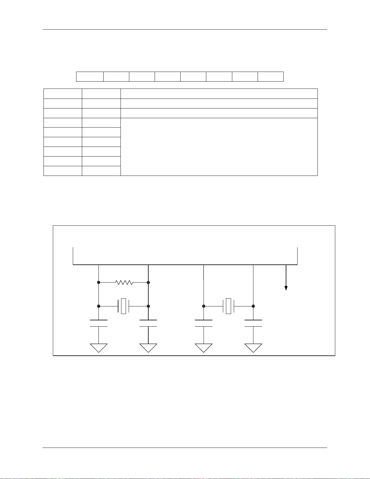
The oscillator circuits are designed to connect directly to standard parallel resonant crystal in a Pierce
oscillator configuration. Each side of the crystal should include a 22pF capacitor to ground for both
oscillator circuits and a 1M resistor is required across the 12MHz crystal.
The CPU clock is available as an output on pin CPUCLK (68-pin version only).
This value determines the ratio of the MPU master clock frequency to
the VCO frequency (MCLK) such that
MPUClk = MCLK/(2 * (MPUCKDiv(5:0) + 1)).
Do not use values of 0 or 1 for MPUCKDiv(n).
Default is 0Ch to set CPCLK = 3.6923MHz.
73S1215F
X12IN
1MΩ
12MHz
22pF 22pF 22pF 22pF
Note: The crystals should be placed as close as possible to the IC, and vias should be avoided.
X12OUT
Figure 4: Oscillator Circuit
X32IN
X32OUT
32KHz
CPUCLK
26 Rev. 1.4
DS_1215F_003 73S1215F Data Sheet
1.7.2 Power Control Modes
The 73S1215F contains circuitry to disable portions of the device and place it into a lower power standby
mode. This is accomplished by either shutting off the power or disabling the clock going to the block. The
miscellaneous control registers MISCtl0, MISCtl1 and the master clock control register (MCLKCtl) provide
control over the power modes. There is also a device power down mode that will stop the core, clock
subsystem and the peripherals connected to it. The PWRDN bit in MISCtl0 will set up the 73S1215F for
power down and disable all clocks except the 32kHz oscillator. The power down mode should only be
initiated by setting the PWRDN bit in the MISCtl0 register and not by manipulating individual control bits in
initiated by setting the PWRDN bit in the MISCtl0 register and not by manipulating individual control bits in
various registers. Figure 5 shows how the PWRDN bit controls the various functions that comprise power
various registers. Figure 5 shows how the PWRDN bit controls the various functions that comprise power
down state.
down state.
Note: the PWRDN Signal is not the direct version of the PWRDN Bit. There are delays from assertion of the
PWRDN bit to the assertion of the PWRDN Signal (32 MPU clocks) Refer to the Power Down sequence diagram.
MISCtl0 - PWRDN
MISCtl1 - ANAPEN
VDDFCtl - VDDFEN
MISCtl1 - USBPEN
ACOMP - CMPEN
MCLCKCtl - 32KEN
MCLCKCtl - HOSEN
SCVCCCtl - SCPRDN
MISCtl1 - FRPEN
These are the registers and
the names of the control bits.
PWRDN Signal
USB
SUSPEND
+
+
+
+
+
+
+
PD_ANALOG
Analog functions
(VCO, PLL,
reference and bias
circuits, etc.)
VDDFAULT
USB Transceiver
(suspend mode)
ANALOG
COMPARE
32K OSC
High Speed OSC
Smart Card Power
Flash Read Pulse
one-shot circuit
These are the
block references.
Figure 5: Power Down Control
When the PWRDN bit is set, the clock subsystem will provide a delay of 32 MPUCLK cycles to allow the
program to set the STOP bit in the PCON register. This delay will enable the program to properly halt the
core before the analog circuits shut down (high speed oscillator, VCO/PLL, voltage reference and bias
circuitry, etc.). The PDMUX bit in SFR INT5Ctl should be set prior to setting the PWRDN bit in order to
configure the wake up interrupt logic. The power down mode is awakened from interrupts connected to
external interrupts 0, 4 and 5 (external USR[0:7], smart card, USB, RTC and Keypad). These interrupt
sources are OR’ed together and routed through some delay logic into INT0 to provide this functionality.
The interrupt will turn on the power to all sections that were shut off and start the clock subsystem. After
the clock subsystem clocks start running, the MPUCLK begins to clock a 512 count delay counter. When
the counter times out, the interrupt will then be active on INT0 and the program can resume. Figure 6
shows the detailed logic for waking up the 73S1215F from a power down state using these specific interrupt
sources. Figure 7 shows the timing associated with the power down mode.
Rev. 1.4 27
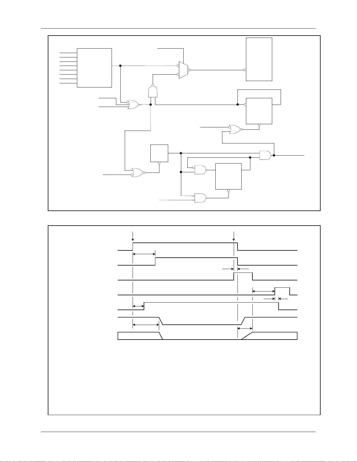
73S1215F Data Sheet DS_1215F_003
PDMUX
USR0
USR1
USR2
USR3
USR4
USR5
USR6
USR7
USR[7:0] Control
USRxINTSrc set to
4(ext INT0 high)
or
6(ext INT0 low)
INT4
INT5
(FF94h:bit7)
MPU
0
1
INT0
CE
9 BIT CNTR
TC
RESETB
Notes:
1. The counters are clocked by the MPUCLK
2. TC - Terminal count (high at overflow)
3. CE - Count enable
Figure 6: Detail of Power Down Interrupt Logic
PWRDN BIT
PWRDN SIG
EXT. EVENT
INT0 to MPU
MPU STOP
CLR
PWRDN_analogQ
D
CLR
RESETB
PWRDN
(FFF1h:bit7)
RESETB
CE
5 BIT CNTR
CLR
TC
t0
t1
t2
text
t4
t6
t7
ANALOG Enable
PLL CLOCKS
t3
t5
t0: MPU sets PWRDN bit
t1: 32 MPU clock cycles after t0, the PWRDN SIG is asserted, turning all analog functions OFF.
t2: MPU executes STOP instruction, must be done prior to t1.
t3: Analog functions go to OFF condition. No Vref, PLL/VCO, Ibias, etc.
text: An external event (RTC, Keypad, Card event, USB) occurs.
t4: PWRDN bit and PWRDN signal are cleared by external event.
t5: High-speed oscillator/PLL/VCO operating.
t6: After 512 MPU clock cycles, INT0 to MPU is asserted.
t7: INT0 causes MPU to exit STOP condition.
Figure 7: Power Down Sequencing
28 Rev. 1.4
DS_1215F_003 73S1215F Data Sheet
External Interrupt Control Register (INT5Ctl): 0xFF94 Å 0x00
Table 15: The INT5Ctl Register
MSB LSB
PDMUX – RTCIEN RTCINT USBIEN USBINT KPIEN KPINT
Bit Symbol Function
When set = 1, enables interrupts from USB, RTC, Keypad (normally going to
int5), Smart Card interrupts (normally going to int4), or USR(7:0) pins (int0) to
cause interrupt on int0. The assertion of the interrupt to int0 is delayed by
INT5Ctl.7 PDMUX
512 MPU clocks to allow the analog circuits, including the clock system, to
stabilize. This bit must be set prior to asserting the PWRDN bit in order to
properly configure the interrupts that will wake up the circuit. This bit is reset
= 0 when this register is read.
INT5Ctl.6 –
INT5Ctl.5 RTCIEN RTC interrupt enable.
INT5Ctl.4 RTCINT RTC interrupt flag.
INT5Ctl.3 USBIEN USB interrupt enable.
INT5Ctl.2 USBINT USB interrupt flag.
INT5Ctl.1 KPIEN Keypad interrupt enable.
INT5Ctl.0 KPINT Keypad interrupt flag.
Miscellaneous Control Register 0 (MISCtl0): 0xFFF1 Å 0x00
Table 16: The MISCtl0 Register
MSB LSB
PWRDN – – – – – SLPBK SSEL
Bit Symbol Function
This bit sets the circuit into a low-power condition. All analog (high speed
oscillator and VCO/PLL) functions are disabled 32 MPU clock cycles after
this bit is set = 1. This allows time for the next instruction to set the STOP bit
MISCtl0.7 PWRDN
in the PCON register to stop the CPU core. The RTC will stay active if it is
set to operate from the 32kHz oscillator. The MPU is not operative in this
mode. When set, this bit overrides the individual control bits that otherwise
control power consumption.
MISCtl0.6 –
MISCtl0.5 –
MISCtl0.4 –
MISCtl0.3 –
MISCtl0.2 –
MISCtl0.1 SLPBK UART loop back testing mode.
MISCtl0.0 SSEL Serial port pins select.
Rev. 1.4 29
73S1215F Data Sheet DS_1215F_003
Miscellaneous Control Register 1 (MISCtl1): 0xFFF2 Å 0x10
Table 17: The MISCtl1 Register
MSB LSB
– – FRPEN FLSH66 – ANAPEN USBPEN USBCON
Bit Symbol Function
MISCtl1.7 –
MISCtl1.6 –
Flash Read Pulse enable (low). If FRPEN = 1, the Flash Read signal is
passed through with no change. When FRPEN = 0 a one-shot circuit that
MISCtl1.5 FRPEN
shortens the Flash Read signal is enabled to save power. The Flash Read
pulse will shorten to 40 or 66ns (approximate based on the setting of the
FLSH66 bit) in duration, regardless of the MPU clock rate. For MPU clock
frequencies greater than 10MHz, this bit should be set high.
MISCtl1.4 FLSH66
When high, creates a 66ns Flash read pulse, otherwise creates a 40ns read
pulse when FRPEN is set.
MISCtl1.3 –
0 = Enable the analog functions that generate VREF and bias current
MISCtl1.2 ANAPEN*
functions. Setting high will turn off the VPD regulator and VCO/PLL
functions.
MISCtl1.1 USBPEN 0 = Enable the USB differential transceiver.
MISCtl1.0 USBCON USB pull-up resistor connect enable.
*Note: The ANAPEN bit should never be set under normal circumstances. Power down control should
only be initiated via use of the PWRDN bit in MISCtl0.
30 Rev. 1.4
 Loading...