


Simplifying System In tegrationTM
73M1966B
Demo Board User Manual
January 22, 2010
Rev. 1.2
UM_1966B_022

73M1966B Demo Board User M anual UM_1966B_022
© 20 08 Teridi an Semiconductor C or porati on. All rights r eserved .
Terid i an Semiconductor Corporation is a registered trademark of Teridi an Semiconductor Corporation.
Windows is a regist er ed trademar k of Mic r osoft Corporation.
All other trademarks ar e the property of thei r r espective owners.
Terid i an Semiconductor Corporation m akes no warranty for the use of its products, other than expressly
contained in the Comp any’s warranty d etailed in the Terid ian S emiconductor Corporation st andar d Terms
and C onditions. The company assu mes no responsib i lity for any errors whi ch may appear in this
document, reserves th e r i ght to change device s or sp ecifications detailed herein at any time withou t
notice and does n ot make any commitm ent to upd ate the information contained herein. Accordingl y, the
reader is cautioned to verify that t his document is current by comparing it to the latest version on
http://www.teridian .com or by checking with your sales represen tative.
Terid i an Semiconductor Corp., 64 40 Oak Canyon, Suite 100, Ir vine, CA 92618
TEL (714) 508-8800, FAX (714) 508-8877, http://www.teridian.com
2 Rev. 1.2

UM_1966B_022 73M1966B Dem o Board User M anual
Table of Contents
1
Introduction...................................................................................................................................... 5
1.1 Packa ge Con tents.................................................................................................................... 5
1.2 Safety and ESD Not es ............................................................................................................. 5
2 Connectors ...................................................................................................................................... 6
3 Connecting the Demo Board into an Existing System ....................................................................... 7
4 Connecting the Demo Board Directly to a PCM Test Set .................................................................. 8
5 73M1966B Demo Board Sch em atics, PCB Layouts and Bil l of Materi als .......................................... 9
5.1 Schematics .............................................................................................................................. 9
5.2 PCB Layouts .......................................................................................................................... 11
5.3 Bill of Materials ...................................................................................................................... 13
6 Ordering Information ...................................................................................................................... 14
7 Related D ocumentation ................................................................................................................. 14
8 Contact Information ....................................................................................................................... 14
Revision History .................................................................................................................................... 15
Rev. 1.2 3

73M1966B Demo Board User M anual UM_1966B_022
Figures
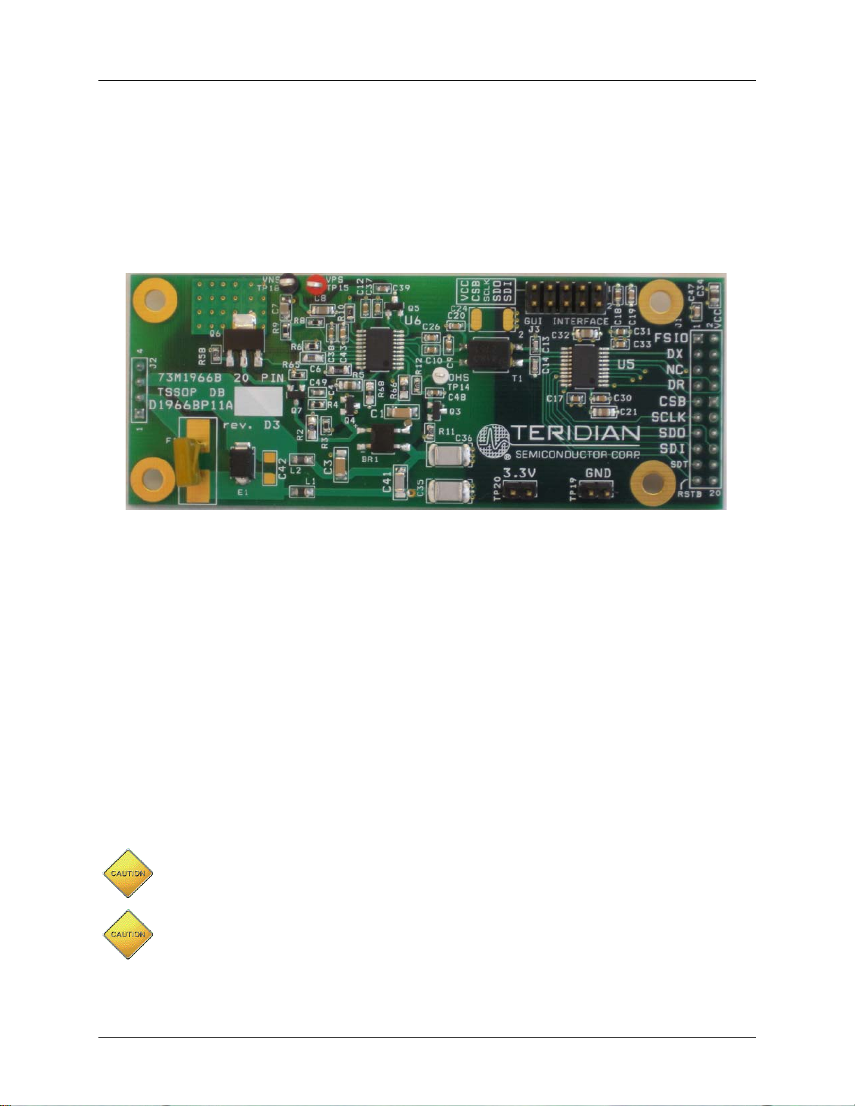
Figure 1: 73M1966B Dem o Boar d
Figur e 2: Co nne ct ing the 73M1966B Demo Board Directly to a PCM Test Set
Figur e 2 : 73M1 9 66B 20-Pin TSSOP Demo Boar d Sch emati c Diagr am Host Interface
Figure 3 : 73M1966B 20-Pin TS SOP Demo Board Schematic Diagram Lin e Interface
Figure 4: 73M1966B Dem o Board Top Layer
Figure 5: 73M1966B Demo Board Bott om Layer
Figur e 6 : 73M1 9 66B 20-Pin TSSOP Demo Boar d: Ground Plane Layer
Figur e 7 : 73M1 9 66B 20-Pin TSS OP Dem o Board: Power Plan e Layer
Tables
Table 2: J1 Pin Descriptions
Table 3: J2 Pin Descriptions
Table 4: J3 Pin Descriptions
Table 1: 73M1966B Demo Boar d Bill of Materials
Table 5: Order Numbers and Packagin g Marks
........................................................................................................... 5
......................................... 8
............................. 9
............................ 10
......................................................................................... 11
.................................................................................... 11
................................................ 11
.................................................. 12
.................................................................................................................... 6
.................................................................................................................... 6
.................................................................................................................... 6
.................................................................................. 13
...................................................................................... 14
4 Rev. 1.2
UM_1966B_022 73M1966B Dem o Board User M anual
1 Introduction
The 73M1966B Demo Board can be used with the 73M1966/1866 Demo Motherboard or in tar get
app l ications where it is connected either by the appropr i ate connector or “blue wired” into the system that
is will be used with. The active circuitry is identical to the 73M1866B Keychain Board other than including
a connector for the GUI interface cable. The GU I cab le is includ ed in the 73M19 66B Evaluation Kit and
the Demo Board kit if it has been sp ecifically ordered.
1.1 Package Contents
Figure 1: 73M1966B Demo Board
The 73M1966B Demo B oar d Kit includ es:
• A 73M1966B D emo Boar d (Rev. D 3)
• GUI Interface Cable (included with 73M1966B-EVM and 73M1966B-DB-C)
• The following documents on CD:
• 73M1966B Dem o Bo ar d User Ma nu al (this document)
• 73M1866B /73M1966B Data Sheet
• 73M1966B GUI User Guide (included with 73M1966B-EVM and 73M1966B-DB-C)
• 73M1966 Layout Guideli n es
• 73M1x66 Worldwi de Desi gn Gui de
• PCM Connectivi ty Application Note
1.2 Safety an d ES D Notes
Connecting live voltages to the 73M1966 Demo Board system will result in p otential l y hazard ous voltages
on the boards.
Extreme caution should be taken when handling the 73M1966B Demo Board after
connection to live voltages!
The 73M1966B Demo Board is ESD sensitive! ESD precautions should be t ak en wh en
handling this board!
Rev. 1.2 5

73M1966B Demo Board User M anual UM_1966B_022
1
FSIO
PCM Bidi r ectional Frame Sync
2
VCC
3.3V power in
3
DX
PCM Receive Digital Data Out pu t
4
VCC
3.3V power in
Pin
Name
Function
1
N/C
No Connect
Pin
Pin N ame
Pin
Pin N ame
9
VCC
10
N/C
No Connect
2 Connectors
This section describes the 73M1966B Demo Board connectors. All the digital signals and power supply
conn ections are made thr ough a 20-pin header connector. The audi o monit or i s also brought ou t on this
connector . Table 1 describes the pins for th e J1 connect or . For convenience, most digital signals are
grouped wit h the PCM si g nals on the odd pins from pin 1 to pin 7, and the PCM CLKI pin is on pin 8. The
SPI signals can be found on the odd pins 9 through 17. Reset is on pin 19. The interrupt output is on pin
16. There are two power pins on pins 2 and 4 and two ground pins on pins 18 and 20. The audio monitor
output ca n be found on pin 10. There is also a C LKO pin that can be used for the rare case where the
73M1866B is used in the master mode.
Table 1: J1 Pi n Descriptions
Pin Pin Nam e
Function Pin Pin Nam e Function
5 N/C No Connect 6 CLKO PCM Highway Clock Output
7 DR PCM Transmit Dig ital Data Input 8 CLKI PCM Highway Clock Input
9 CSB Chip Select - low true 10 AUDIO Aud i o output for speaker
11 SCLK SPI Clock 12 N/C No Connect
13 SDO Serial Contr ol Data Out 14 N/C No Connect
15 SDI Serial Control Data In 16 INTB Interrupt Output - low tru e
17 SDT
Serial Data Thru – used in Daisy
Chain Mode
18 GND Ground
19 RSTB Reset - low true 20 GND Ground
Table 2 descr i bes t he J2 connector pins. These ar e the bi-directional PSTN network connections that
pass the audio si gnals to and from th e FXO.
Table 2: J2 Pi n Descriptions
2 TIP Bidi r ectional Analog Signaling
3 RING Bidirect ional Analog Signaling
4 N/C No Connect
The signals on the TIP and RING pins should also have a DC current that would normally come from the
PSTN. This current will usually be in the range of 20 to 100 mA, but typically about 40 mA. This current
is n ecessary for the F XO t o operate norm ally. The FXO will not operate if the current drops b elow
approximately 13 mA.
Table 5 describes the J3 connector pins. J3 is use d to co nnect a host P C to the Dem o Board to provide
GUI control.
Table 3: J3 Pi n Descriptions
1 SDI Serial Control Data In 2 N/C No Conn ect
3 SDO Serial Control Data Out 4 GND
5 SCLK Serial Clock 6 GND
7 CSB Chip Select - low true 8 GND
6 Rev. 1.2
Function
Function

UM_1966B_022 73M1966B Dem o Board User M anual
3 Connecting the Demo Board into an Existing System
The 73M 1966B Keychain Demo Board is desi gned to be easily connected to an existing system that has
access to a PCM and SPI in terface. Table 1 provides the pin and signal names. Further detail i s
provided in the 73M1866B/73M1966B Data Sheet. If con nect i vity betwe en the Keychain D emo Board
and the system is pr ovided by ‘blue-wire’, we recommend that 30 AWG wire be used as a minimum and
that the maximum l ength of these wires should not exceed 8 inch es (20 cm). It i s also recom men ded that
the ground have at least two 30 AWG wires connecting the 73M1966B Demo Board to the host board.
Once connected , the user should ch eck for the integrity of ap prop r i ate clock and control si gnal s. Ensure
the signal s have m i nimal over-shoot and und er -shoot on the signal transitions. Consult the
73M1866B /1966B Data Sheet for information on the sig nal timing and ensu r e the host SPI conform s to
these requirements.
The 73M1966B Demo Board is also designed t o pl ug in to the 73M1966B EVM Moth er board . This board
supports the con nect i on of a PCM test device such as the Wandel and Goltermann PC M -4. See the
73M1966B-EVM User M an ual for more information.
In or der for the 73M1966B Dem o Board to operate co r rectly it n eeds t o be configured by soft ware.
Teridian provided Reference Driver Software and Linux based Command Line application can be used to
configure and contr ol the 73M 1966B. Contact Teridi an Sales for more in formation on the available
software.
If 73M1966B-DB-C has been p r ovided, a cable is includ ed that connects the GUI Interface J3 to a
Windows PC wit h a parallel por t. Thi s, along with the GUI software, will allow a user to configure the
73 M1 966B wit hout the n eed to provide any embed ded software. Refer t o the 73M1966B GUI User Guide
for more informati on on using the Terid i an pr ovided GUI softwar e.
If a 73M1966B Motherboard Evaluation Kit (73M1966B-EVM) is b eing used, the 73M 1966B Dem o Board
is inserted in to the app r opriat e socket . For further details on operating this sy stem, r efer to the
73M1966B EVM User Manual.
Rev. 1.2 7

73M1966B Demo Board User M anual UM_1966B_022
RSTB
TO TRANSMIT CLOCK OF TEST SET
AUDIO
TO TRANSMIT DATA OUTPT OF TEST SET
TO RECEIVE DATA INPUT OF TEST SET
J1
DIGITAL HEADER 10X2
2
4
6
8
10
12
14
16
18
20
1
3
5
7
9
11
13
15
17
19
SDT
TO FRAME SYNC OUTPUT OF TEST SET
VCC3.3
3.3V DC POWER INPUT
INTB
CLKO
J2
ANALOG HEADER
1
2
3
4
CSB
VCC3.3
SDI
SDO
J3
GUI HEADER 5x2
2
4
6
8
10
1
3
5
7
9
SDI
SDO
SCLK
SCLK
CSB
GND
ANA
ANA
4 Connecting the Demo Board Directly to a PCM Test Set
The 73M1966B Demo Motherboard co nveniently p r ovides a po wer connector, a power sw itch, P C M
interface conn ectors, and clock co nnectors. However, it is not n ecessary t o util ize the Motherboard when
evalu ating the device set . In some applica tions, it might be b etter to direct ly connect the 73 M1 966B
Demo Board to th e PC M channel test set. Even without the Motherboard, the 73M1966B can be used
with the G U I and a ch annel test set.
If onl y t he 73M1966B Dem o Board is used, the two-row J1 co nnector h as all the necessary signals to
connect to the digital signals of the channel test set and 3.3 V power as shown in Figure 2. Other PCM
highway test sets should also requir e only the 73M1966B Demo Board to perform similar tests.
Figure 2: Connecting the 73M1966B Demo Board Directly to a PCM Test Set
8 Rev. 1.2

73 M1 966B Demo Board User Man ual UM_1966B_022
TP19
1
2
TP20
1
2
SDI
RSTB
SCLK
SDO
SDI
J3
GUI INTERFACE
2
4
6
8
10
1
3
5
7
9
CSB
AUDIO
U5
73M1906-20
CS
1
AOUT
9
VPD
2
VPT
14
PCLKO
6
PCLKI
7
SCLK
20
DX
4
DR
3
FSIO
5
SDITHRU
16
SDO
18
SDI
17
VPPLL
10
VNPLL
8
PRM
12
PRP
13
RST
15
VNT
11
INT
19
CLKI
C19
1nF
CSB
AUDIO
INTB
VCC
DR
C30
1nF
DX
VCC
DX
J1
CON N SOC KET 10X2
2
4
6
8
10
12
14
16
18
20
1
3
5
7
9
11
13
15
17
19
+
C21
3.3uF
C33
1nF
+
C32
3.3uF
SDT
PRM
PRP
FSIO
VCC
FSIO
SCLK
C17
0.1uF
C47
1nF
C31
0.1uF
C34
10uF
VCC
C18
0.1uF
VCC
CLKO
CLKI
CLKO
INTB
SDO
5 73M1966B Demo Board Schematics, PCB Lay outs an d B ill of Mat er ial s
5.1 Schematics
Figure 3 : 73M1966B 20-Pin TSSOP Demo Board Schematic Diagram Host I nterface
Rev. 1.2 9

73 M1 966B Demo Board User Man ual UM_1966B_022
R2
10M, 0805
R12 5.1K
R11
5.1K
* Optional, see layout design guide
Q7
MMBTA42
1
32
R68
1M, 0805
C3 0.022uF, 250V
C48
0.1uF
Q6
BCP-56
1
23
4
C49
100pF
C36
220pF, 3KV
C35
220pF, 3KV
C1 0.022uF, 250V
C4
10uF
C39
5600pF
R8
52.3K, 1%
R9
21K, 1%
R5 8.2, 1%, 0805
R3 412K, 1%
U6
73M1916-20
OFH
4
VNX
5
SCP
6
MID
7
VPX
8
VBG
11
ACS
12
SRE
9
SRB
10
VNS
13
VPS
14
RXP
15
RXM
16
TXM
17
DCS
19
DCD
18
DCI
1
RGN
2
RGP
3
DCG
20
R66
1M, 0805
R6
17.4K, 1%
C38
0.1uF
C12
0.1uF
R4
100K, 1%
C7 4.7uF
C41
220pF, 630V
-+
BR1
HD04
4
1
3
2
TP18
VNS
1
C37
0.01uF
TP14
OFH
1
TP15
VPS
1
R58 240
L1
2 kOhm@100MHz
DCS
C9
0.22uF
T1
Pulse TFR
1
4
2 3
F1
TRF600-150
L2
2 kOhm@100MHz
C10
0.22uF
+
C8
4.7uF
R10
174, 1%
TB03100H
Q3
MMBTA42
1
32
J2
4 HEADER
1
2
3
4
C6
4.7uF
R65 200
Q4
MMBTA92
1
3 2
E1
P3100SBRP
Q5
MMBTA06
1
32
PRM
PRP
C24
NC(1nF, 3KV)
C13
15pF
C26
1nF
OHS
VNS
C14
15pF
VBG1916
RGP
SRE
ACS
SRB
C42
NC
DCI
RGN
D1
MMSZ475253BT1*
C20
1nF
C43
1nF
NOTE: GND f or C 35 and
C36 should be on t he hos t
side of the barrier
Figure 4 : 73M1966B 20-Pin TSSOP Demo Board Schematic Diagram Line Interface
10 Rev. 1.2

73 M1 966B Demo Board User Man ual UM_1966B_022
5.2 PCB Layouts
Figure 5: 73M1966B Demo Board Top Layer
Figure 6: 73M1966B Demo Board Bottom Layer
Figure 7 : 73M1966B 20-Pin TSSOP Demo Board: Ground Plane Layer
Rev. 1.2 11

73 M1 966B Demo Board User Man ual UM_1966B_022
Figure 8 : 73M1966B 20-Pin TSSOP Demo Board: Power Plane Layer
12 Rev. 1.2

UM_1966B_022 73M1966B Dem o Board User M anual
2
C1, C3
0.022µF, 250V
TDK
C3216X7R2E223K
C31, C38, C48
5.3 B ill of Materials
Table 4 provides the bi ll of materials for the 73M1966B Dem o Board schem atic provided in Figure 3 and
Figure 4.
Table 4: 73M1 966B Dem o Board Bill of Materials
Qty Reference Part Description Source Example MFR P/N
1 BR1 HD04 rectifier bridge, 0.8A, 400V Diodes Inc. HD04-T
2 C4, C34 10 µF AVX, Panasonic TCP0J106M8RA
3 C6, C7, C8 4.7μF 25V, X5R, 0805 AVX, Panasonic 08053D475KAT2A
2 C9, C10 0.22μF 16V, X7R, ceramic, 0603 Panasonic C0603C224K8RACTU
C12, C17,C18,
6
2 C13, C14 15pF 50V, ceramic, 0603 Panasonic ECJ-1VC1H150J
C19, C20, C26,
7
C30, C33, C43,
C47
2 C21, C32 3.3μF 6.3V, tantalum, 0805 Rohm TCP0J335M8R
2 C35, C36 220pF, 3KV Kemet C1812C102KHRACTU
2 C37, C39 0.01μF 50V, X7R, ceramic, 0603 AVX, Panasonic 06035C103KAT2A
1 C41 220pF, 630V TDK C3216COG2J221J
1 C49 100pF Panasonic ECJ-1CV1H101J
1 E1 P3100SBRP Teccor P3100SBLRP
1 F1 TRF600-150 Raychem TRF600-150
1 J1 Header Sullins 10 X 2
1 J2 Header Sullins 4 X 1
1 J3 Header Sullins 5 X 2
2 L1, L2 2000 Ohm TDK MPZ2012S601A
1 Q5 MMBTA06, NPN 80 V transistor SOT23
1 Q4 MMBTA92, PNP 300 V transistor SOT23
2 Q3, Q7 MMBTA42, NPN 300 V transistor SOT23
1 Q6 NPN 80 V transistor SOT223 Fairchild, On Semi BCP56
1 R2 10M, 5%, 1/8W resistor 0805 Yageo RC0805JR-0710ML
1 R3 412K, 1%, 1/10W resistor 0603 Yageo RC0603FR-07412KL
1 R4 100K, 1%, 1/10W resistor 0603 Yageo RC0603FR-07100KL
1 R5 8.2, 5%, 1/8W resistor 0805 Yageo RC0805JR-078R2L
1 R6 17.4K, 1%, 1/10W resistor 0603 Yageo RC0603FR-0717K4L
1 R8 52.3K, 1%, 1/10W resistor 0603 Yageo RC0603FR-0752K3L
1 R9 21K, 1%, 1/10W resistor 0603 Yageo RC0603FR-0721KL
1 R10 174, 1%, 1/10W resistor 0603 Yageo RC0603FR-07174RL
1 R11 3K, 5%, 1/10W resistor 0603 Yageo RC0603JR-073K0L
1 R12 5.1 K, 5%, 1/10W resistor 0603 Yageo RC0603JR-075K1L
1 R58 240, 5%, 1/10W resistor 0603 Yageo RC0603JR-07240RL
1 R65 200, 5%, 1/10W resistor 0603 Yageo RC0603JR-07200RL
2 R66, R68 1 M, 5%, 1/8W resistor 0805 Yageo RC0603JR-071ML
1 T1 Pulse transf or mer
0.1μF 16V, X7R, ceramic, 0603 Panasonic, Kemet C0603C104K8RACTU
1nF 10V, X7R, ceramic, 0603 Panasonic C0603C102K8RACTU
Diodes, Fairchild,
Central, On Semi
Diodes, Fairchild,
Central, On Semi
Diodes, Fairchild,
Central, On Semi
UMEC, Sumida,
Midcom
MMBTA06LT1G
MMBTA92LT1G
MMBTA42LT1G
UBT 015 4, ESM IT
418 0, 750110001
Rev. 1.2 13

73 M1 966B Demo Board User Man ual UM_1966B_022
6 Ordering Information
Table 5 l i sts the order numbers and packaging marks used to identify 73M1966B and 73M1866B Demo
Boards.
Table 5: Order Numbers and Packaging Marks
Part Description Orde r Number Packaging Mark
73M1966B 20-Pin TSSOP Motherboard and
Standard Demo Board
73M1966B 20-Pin TSSOP Demo Board 73M1966B-DB 73M1966B-IM
73M1966B 20-Pin TSSOP Demo Board with GUI cable 73M1966B-DB-C 73M1966B-IM
73M1866B 20-Pin TSSOP Keychain Dem o Board 73M1866B-Keychain
73M1966B-EVM 73M1916-M
73M1906B
7 Related Documentation
The following 73M1x6 6B document s are available from Teri dian Semi conductor C orp or ation:
73M1866B /73M1966B Data Sheet
73M1866B/73M1966B Layout Guidelines
73M1x66 Worldwi de Desi gn Gui de
73M1x66 PCM Connectivity Application Note
73M1966B-EVM User M an ual
73M1966B GUI User Guide
73M1866B /73M1966B FXOCTL Ap plica tion U ser Guide
8 Contact Information
For m or e i nform ation about Teridian Semiconductor pr oducts or to check the availability of the
73M1966B, contact us at :
644 0 Oak Canyon Road
Suite 100
Irvin e, CA 92618-5201
Telephone: (714) 508-8800
FAX: (714) 508-8878
Email: modem.support@teridian.com
For a complete list of worldwide sa les offic es, g o to http://www.teridian.com.
14 Rev. 1.2
 Loading...