

TERIDIAN Semiconductor 71M6545, 71M6545H User Manual
71M6545/71M6545
H
s
A Maxim Integrated Product s Brand
19-5378; Rev 1.0; 4/ 11
MPU
RTC
TIMERS
XIN
XOUT
RX
V3P3A V3P3SYS
VBAT_RTC
GNDA GNDD
DIO
ICE
LOAD
DIO
SERIAL PORT
OSCILLATOR/
PLL
MUX and ADC
DIO, PULSES,
LEDs
COMPUTE
ENGINE
FLASH
MEMORY
RAM
32 kHz
REGULATOR
POWER SUPPLY
TERIDIAN
71M6545/H
TEMPERATURE
SENSOR
VREF
PWR MODE
CONTROL
PB
NEUTRAL
I2C or µWire
EEPROM
10/7/2010
RTC
BATTERY
V3P3D
BATTERY
MONITOR
SPI INTERFACE
HOST
WPULSE
RPULSE
SPI_CKI
SPI_CSZ
SPI_DI
SPI_DO
XFER_BUSY
XPULSE
YPULSE
SAG
TX
3.3 VDC
PULSES
24
T
M
U
X
IADC0
VADC8 (VA)
IADC2
VADC9 (VB)
IADC4
VADC10 (VC)
C
B
A
NEUTRAL
Shunt Resistor Sensors
IADC6
IADC1
IADC3
IADC5
IADC7
Resistor Dividers
Pulse Transformers
A
B
C
}
IN*
}
IA
}
IB
}
IC
71M6xx3
71M6xx3
71M6xx3
This system is referenced to Neutral
*IN = Optional Neutral Current
Metrology Processor
April 2011
GENERAL DESCRIPTION
The 71M6545/71M6545H metrology processors are based on
Teridian’s 4th-generation metering architecture supporting the
71M6xxx series of isolated current sensing products that offer
drastic reduction in component count, immunity to magnetic
tampering, and unparall eled reli abilit y. The 71M6545/71M6545H
integrate our Single Conv erter Technology® with a 22-bit deltasigma ADC, a customizable 32-bit computation engine (CE) for
core m etrology functions, as well as a user-programm able 8051compatible application processor (MPU) core with up to 64KB
flash and up to 5KB RAM.
An external host processor can access metrology functions directly through the SPI™ interface, or alternatively through the
embedded MPU core in applications requiring metrology data
capture, storage, and preprocessing within the metrology
subsystem. In addition, the devices integrate an RTC, DIO , and
UART. A complete array of ICE and development tools,
programming libraries, and reference designs enable rapid
development and certification of meters that meet all ANSI and
IEC electricity metering standards worldwide.
Single Converter Technology is a registered trademark of Maxim Integrated Products, Inc.
SPI is a trade mar k of M ot or o la, Inc.
MICROWIRE is a registered trade mark of National Semiconductor Corp.
v1.0 © 2008–2011 Teridian Semiconductor Corporation 1
D ATA SHEET
FEATURES
• Up to < 0.1% Accuracy Over 2000:1
Current Range
• Exceeds IEC 62053/ANSI C12.20 Standards
• Seven Sensor Inputs with Neutral Current
Measurement, Differential Mode Selectable
for Current Inputs
• Selectable Gain of 1 or 8 f or On e Cur r ent
Input to Support Shunts
• High-Speed Wh/VARh Pulse Outputs with
Programmable Width
• Flash/RAM Size
32KB/3KB (71M6545)
64KB/5KB (71M6545H)
• Up to Four Pulse Outputs with Pulse Count
• Four-Quadrant M etering, Phase
Sequencing
• Digital T em per ature Compensation
Metrology Compensation
Accurate RTC for TOU Functi ons with
Automatic Temper ature Compensation
for Crystal in All Power Modes
• Independent 32-Bi t Compute Engine
• 46–64Hz Line Frequen c y Range with the
Same Calibration
• Phase Compensation (±7°)
• 1µA Supply Current in Sleep Mode
• Flash Securit y
• In-System Program Update
• 8-Bit MPU (80515), Up to 5 MIPS, for
Optional Implementation of Postprocessing
and Host Support Functions (Optional Use)
• Up to 29 DIO Pins
• Hardware Watchdog Timer (WDT)
2
• I
C/MICROWIRE® EEPROM Inter face
• SPI Interface for Host:
Full Access to Shared Memory Space
Flash Program Capability
• UART
• Industrial Temperature Range
• 64-Pin Lead(Pb)-Free LQFP Package

Data Sheet 71M6545/H PDS_6545_009
Table of Contents
1 INTRODUCTION ........................................................................................................................... 10
2 Hardware Descript io n .................................................................................................................. 11
2.1 Hardware Overview............................................................................................................... 11
2.2 Analog Front End (AFE ) ........................................................................................................ 12
2.2.1 Signal Input Pins ....................................................................................................... 13
2.2.2 Input Multipl ex er ........................................................................................................ 14
2.2.3 Delay Compensation ................................................................................................. 19
2.2.4 ADC Pre-Amplifier ..................................................................................................... 20
2.2.5 A/D Converter (ADC) ................................................................................................. 20
2.2.6 FIR Filter ................................................................................................................... 20
2.2.7 Volt age References ................................................................................................... 20
2.2.8 71M6xx 3 Isolated Sensor Interface ............................................................................ 21
2.3 Digital Computation Engine (CE) ........................................................................................... 25
2.3.1 CE Program Memory ................................................................................................. 25
2.3.2 CE Data Memory ....................................................................................................... 25
2.3.3 CE Communi c ation with the MPU .............................................................................. 25
2.3.4 Meter Equations ........................................................................................................ 26
2.3.5 Real-Time Monitor (RTM) .......................................................................................... 26
2.3.6 Pulse Generators ...................................................................................................... 26
2.3.7 CE Functi onal Overview ............................................................................................ 28
2.4 80515 MPU Core .................................................................................................................. 30
2.4.1 MPU Setup Code ...................................................................................................... 30
2.4.2 80515 MPU Overview ................................................................................................ 30
2.4.3 Memory Organization and Addressing ....................................................................... 31
2.4.4 Special Function Registers (SFRs) ............................................................................ 33
2.4.5 Generi c 80515 Special Function Registers ................................................................ 33
2.4.6 Instruct ion Set ........................................................................................................... 36
2.4.7 UARTs ...................................................................................................................... 36
2.4.8 Tim ers and Counters ................................................................................................. 38
2.4.9 WD Timer (Software Watchdog Timer) ...................................................................... 40
2.4.10 Interrupts ................................................................................................................... 40
2.5 On-Chip Resources............................................................................................................... 46
2.5.1 Physical Memory ....................................................................................................... 46
2.5.2 Oscillator ................................................................................................................... 48
2.5.3 PLL and Inter nal Clocks............................................................................................. 48
2.5.4 Real-Tim e Cloc k (RT C) ............................................................................................. 49
2.5.5 71M6545/H Tem per ature Sensor ............................................................................... 53
2.5.6 71M6xx3 Temperature Sensor .................................................................................. 54
2.5.7 71M6545/H Battery Monitor ....................................................................................... 55
2.5.8 71M6xx3 VCC Monitor .............................................................................................. 55
2.5.9 UART Interface ......................................................................................................... 55
2.5.10 DIO Pins ................................................................................................................... 55
2.5.11 EEPROM Interface .................................................................................................... 57
2.5.12 SPI Slave Port ........................................................................................................... 60
2.5.13 Hardware Watchdog Timer ........................................................................................ 64
2.5.14 T est P or ts (TMUXOUT and TMUX2OUT Pins)........................................................... 64
3 Functional Description ................................................................................................................ 66
2 © 2008–2011 Teridian Semiconductor Corporation v1.0

PDS_6545_009 Data Sheet 71M6545/H
3.1 Theory of Operation .............................................................................................................. 66
3.2 SLP Mode (Sleep Mode) ....................................................................................................... 67
3.3 Fault and Reset Behavi or ...................................................................................................... 68
3.3.1 Events at Power-Down .............................................................................................. 68
3.3.2 Reset Sequence ........................................................................................................ 69
3.4 Data Flow and Host Communi c ation ..................................................................................... 69
4 Application Information ............................................................................................................... 71
4.1 Connecting 5 V Devic es ........................................................................................................ 71
4.2 Directly Connected S ensors .................................................................................................. 71
4.3 Systems Using 71M6xx3 Isolated Sensors and Current Shunts ............................................. 72
4.4 System Using Current Transformers ..................................................................................... 73
4.5 Metrology Temper ature Compensation .................................................................................. 74
4.5.1 Disti nc tion Between Standard and High-Precision Parts ............................................ 74
4.5.2 Temperat ur e Coeff icients for the 71M6545 ................................................................ 75
4.5.3 Temperat ur e Coeff icients for the 71M6545H .............................................................. 75
4.5.4 Temperat ur e Coeff icients for the 71M6603 and 71M6103 (1% Ener gy A c c ur acy) ...... 75
4.5.5 Temperat ur e Com pensation for VREF and Shunt Sensors ........................................ 75
4.5.6 Temperature Compensation of VREF and Current Transformers ............................... 77
4.6 Connecting I2C EEPROMs .................................................................................................... 79
4.7 Connecting Thr ee-Wire EEPROMs ....................................................................................... 79
4.8 UART (TX/RX) ...................................................................................................................... 79
4.9 Connecting the Reset Pi n ...................................................................................................... 79
4.10 Connecting the Emulator Port Pins ........................................................................................ 80
4.11 Flash Programming ............................................................................................................... 80
4.11.1 Flash Programming via the ICE Port .......................................................................... 80
4.11.2 F lash Programming via the SPI Port .......................................................................... 80
4.12 MPU Demonstration Code..................................................................................................... 81
4.13 Crystal O scillator ................................................................................................................... 81
4.14 Meter Cali br ation ................................................................................................................... 81
5 Firmware Interface ....................................................................................................................... 82
5.1 I/O RAM Map –Functional Order ........................................................................................... 82
5.2 I/O RAM Map – Alphabetical Order ....................................................................................... 88
5.3 Reading the Inf o Page (71M6545H only) ............................................................................... 98
5.4 CE Interface Descri ption ..................................................................................................... 100
5.4.1 CE Program ............................................................................................................ 100
5.4.2 CE Data Format ...................................................................................................... 100
5.4.3 Constants ................................................................................................................ 100
5.4.4 Environment ............................................................................................................ 101
5.4.5 CE Calculations ....................................................................................................... 101
5.4.6 CE Front End Dat a (Raw Data)................................................................................ 102
5.4.7 CE Stat us and Contr ol ............................................................................................. 103
5.4.8 CE Transfer Variables ............................................................................................. 105
5.4.9 Pulse Generation..................................................................................................... 107
5.4.10 CE Calibration Paramet er s ...................................................................................... 110
5.4.11 CE Flow Diagrams .................................................................................................. 111
6 71M6545/H Specif ications ......................................................................................................... 113
v1.0 © 2008–2011 Teridian Semiconductor Corporation 3

Data Sheet 71M6545/H PDS_6545_009
6.1 Absolute Maximum Ratings ................................................................................................. 113
6.2 Recommended External Com ponents ................................................................................. 114
6.3 Recommended Operating Conditions .................................................................................. 114
6.4 Performance Specifications ................................................................................................. 115
6.4.1 Input Logic Levels ................................................................................................... 115
6.4.2 Output Logic Lev els ................................................................................................. 115
6.4.3 Battery Monitor ........................................................................................................ 116
6.4.4 Temperat ur e M onitor ............................................................................................... 117
6.4.5 Supply Cur r ent ........................................................................................................ 118
6.4.6 V3P3D Switch ......................................................................................................... 118
6.4.7 Internal Power Fault Comparators ........................................................................... 119
6.4.8 2.5 V Volt age Regulator – System Power ................................................................ 119
6.4.9 Crystal Oscillator ..................................................................................................... 119
6.4.10 Phase-Locked Loop (PLL) ....................................................................................... 120
6.4.11 71M6545/H VREF ................................................................................................... 121
6.4.12 ADC Converter (71M6545/H) ................................................................................... 122
6.4.13 Pre-Amplifier for IADC0-IADC1 ................................................................................ 123
6.5 Timing Specifications .......................................................................................................... 124
6.5.1 Flash Memor y ......................................................................................................... 124
6.5.2 SPI Slave ................................................................................................................ 124
6.5.3 EEPROM Interface .................................................................................................. 124
6.5.4 RESET Pin .............................................................................................................. 125
6.5.5 Real-Tim e Cloc k (RT C) ........................................................................................... 125
6.6 64-Pin LQFP Package Outline Drawing ............................................................................... 126
6.7 71M6545/H Pinout .............................................................................................................. 127
6.8 71M6545/H Pin Descriptions ............................................................................................... 128
6.8.1 71M6545/H Power and Ground P ins ........................................................................ 128
6.8.2 71M6545/H Analog Pins .......................................................................................... 129
6.8.3 71M6545/H Di gital Pins ........................................................................................... 130
6.8.4 I/O Equivalent Circuits ............................................................................................. 131
7 Ordering Informat io n ................................................................................................................. 132
7.1 71M6545/H Ordering Guide ................................................................................................ 132
8 Related Information ................................................................................................................ 132
9 Conta ct In fo r mation ................................................................................................................ 132
Appendix A: Acronyms .................................................................................................................... 133
Appendix B: Revision Histo ry .......................................................................................................... 134
4 © 2008–2011 Teridian Semiconductor Corporation v1.0

PDS_6545_009 Data Sheet 71M6545/H
Figures
Figure 1: IC Functi onal Bl oc k Di agr am
Figure 2: AFE Block Diagram ( S hunts: One-Local, Three-Remotes)
Figure 3. AFE Block Diagram (Four CTs)
Figure 4: States in a Multiplexer Frame (MUX_DIV[3:0] = 6)
Figure 5: States in a Multiplexer Frame (MUX_DIV[3:0] = 7)
Figure 6: General Topology of a Chopped Amplifier
Figure 7: CROSS Signal wit h CHOP_E = 00
Figure 8: RTM Timing
Figure 9. Pulse Generat or FIFO Timing
Figure 10: Samples from Multiplexer Cycle (Frame)
Figure 11: Accum ulation Interval
Figure 12: Interrupt Structure
Figure 13: Automatic Temperatur e Com pensation
Figure 14: Connecting an External Load to DIO Pins
Figure 15: 3-wire Interface. Write Command, HiZ=0.
Figure 16: 3-wire Interface. Write Command, HiZ=1
Figure 17: 3-wire Interface. Read Command.
Figure 18: 3-Wire Int erfac e. Write Command when CNT=0
Figure 19: 3-wire Interface. Write Command when HiZ=1 and WFR=1.
Figure 20: SPI Slave Port - Typical Multi-Byte Read and Write oper ations
Figure 21: Voltage, Current, Momentary and Accumulated Energy
Figure 22: Data Flow
Figure 23: Resistive Voltage Divider (Voltage Sensing)
Figure 24. CT with Single-Ended Input Connection (Current Sensing)
Figure 25: CT with Differenti al Input Connec tion (Current Sensing)
Figure 26: Diff er ential Resistive Shunt Connections (Curr ent Sensing)
Figure 27: System Usi ng Three-Rem otes and One-Local (Neutral) Sensor ............................................ 72
Figure 28. System Usi ng Cur r ent T r ansformers
Figure 29: I
Figure 30: Connections for the UART
Figure 31: External Components for the RESET Pin: Push-Button (Lef t), Production Circuit ( Right)
Figure 32: External Components for the Emulator Interface
Figure 33. Trim Fuse Bit Mapping
Figure 34: CE Data Flow: Multi plexer and ADC
Figure 35: CE Data Flow: Scaling, Gain Control, Intermediat e V ari ables for one Phase
Figure 36: CE Data Flow: Squar ing and Summation Stages
Figure 37: 64-pin LQFP Pac k age Outli ne
Figure 38: Pinout for the LQFP-64 Package
Figure 39: I/O Equivalent Circuits
2
C EEPROM Connection ...................................................................................................... 79
..................................................................................................... 9
...................................................... 12
............................................................................................... 13
.................................................................. 17
.................................................................. 17
............................................................................... 21
........................................................................................... 21
............................................................................................................................ 26
................................................................................................. 28
............................................................................... 29
............................................................................................................ 29
................................................................................................................. 45
................................................................................. 52
............................................................................. 57
............................................................................. 59
.............................................................................. 59
........................................................................................ 59
................................................................... 59
................................................. 60
.............................................. 61
......................................................... 66
............................................................................................................................. 70
.......................................................................... 71
.................................................... 71
........................................................ 71
................................................... 71
..................................................................................... 73
.................................................................................................... 79
....... 80
................................................................... 80
.......................................................................................................... 98
.................................................................................... 111
........................ 111
................................................................. 112
............................................................................................. 126
......................................................................................... 127
......................................................................................................... 131
v1.0 © 2008–2011 Teridian Semiconductor Corporation 5

Data Sheet 71M6545/H PDS_6545_009
Tables
Table 1. Required CE Code and Set tings for 1-Local / 3-Remotes
Table 2. Required CE Code and Set tings for CT Sensors
Table 3: Multiplexer and A DC Configuration Bits
Table 4. RCMD[4:0] Bits
Table 5: Remote Interfac e Read Commands
Table 6: I/O RAM Control Bits for I sol ated Sensor
Table 7: Inputs Selected in Multiplexer Cycles
Table 8: CKMPU Clock Frequencies
Table 9: Memory Map
Table 10: Inter nal Data Memory Map
Table 11: Special Func tion Register Map
Table 12: Generic 80515 SFRs - Locati on and Reset V alues
Table 13: PSW Bit Functions (SFR 0xD0)
Table 14: Port Register s (DI O0-14)
Table 15: Stretch M em ory Cycl e Width
Table 16: Baud Rate Generat ion
Table 17: UART Modes
Table 18: The S0CON (UART0) Register (SFR 0x 98)
Table 19: PCON Register Bi t Description (SFR 0x87)
Table 20: Timers/Counters Mode Description
Table 21: Allowed Timer /Counter Mode Combinations
Table 22: TMOD Regi ster Bit Description (SFR 0x89)
Table 23: The TCON Register Bit Functions (SFR 0x88)
Table 24: The IEN0 Bit Functions (SFR 0xA8)
Table 25: The IEN1 Bit Functions (SFR 0xB8)
Table 26: The IEN2 Bit Functi ons (SFR 0x9A)
Table 27: TCON Bit Functi ons (SFR 0x88)
Table 28: The T2CON Bit F unctions (SFR 0xC8)
Table 29: The IRCON Bit Func tions (SFR 0xC0)
Table 30: External MPU Interrupts
Table 31: Inter r upt Enable and Flag Bits
Table 32: Inter r upt Pri ori ty Level Groups
Table 33: Inter r upt Pri ori ty Levels
Table 34: Inter r upt Pri ori ty Registers (IP0 and IP1)
Table 35: Inter r upt Polling Sequence
Table 36: Inter r upt Vector s
Table 37: Flash Memory Access
Table 38: Flash Securit y
Table 39: Clock System Summ ar y
Table 40: RTC Control Regi ster s
Table 41: I/O RAM Registers for RTC Temperature Compensation
Table 42: I/O RAM Registers for RTC Interrupts
Table 43: I/O RAM Registers for Temperature and Battery Measurement
Table 44: Data/Dir ec tion Registers and Internal Resources for DIO0 to DIO14
Table 45: Data/Dir ec tion Registers for DIO19-25 and DIO28-29
Table 46: Data/Dir ec tion Registers for DIO55
Table 47: Selectable Resources using the DIO_Rn[2:0] Bits
Table 48: EECTRL Bits for 2-pin Interface
......................................................... 15
...................................................................... 16
................................................................................... 19
........................................................................................................................ 22
........................................................................................ 23
................................................................................. 23
....................................................................................... 26
...................................................................................................... 30
............................................................................................................................ 31
..................................................................................................... 33
............................................................................................... 33
................................................................. 33
............................................................................................... 35
........................................................................................................ 35
.................................................................................................. 36
............................................................................................................ 37
......................................................................................................................... 37
............................................................................. 38
.............................................................................. 38
........................................................................................ 38
........................................................................... 39
............................................................................ 39
........................................................................ 39
........................................................................................ 40
........................................................................................ 41
........................................................................................ 41
............................................................................................. 41
................................................................................... 41
.................................................................................... 42
......................................................................................................... 42
................................................................................................ 43
................................................................................................ 43
.......................................................................................................... 44
................................................................................. 44
..................................................................................................... 44
.................................................................................................................... 44
............................................................................................................ 46
........................................................................................................................ 47
......................................................................................................... 49
........................................................................................................... 50
........................................................ 51
.................................................................................... 52
.............................................. 54
....................................... 55
............................................................. 56
........................................................................................ 56
................................................................... 56
............................................................................................... 57
6 © 2008–2011 Teridian Semiconductor Corporation v1.0

PDS_6545_009 Data Sheet 71M6545/H
Table 49: EECTRL B its for the 3-wir e Interface ....................................................................................... 58
Table 50: SPI Transacti on Fields
Table 51: SPI Command Sequenc es
Table 52: SPI Register s
Table 53: TMUX[4:0] Selections
Table 54: TMUX2[4:0] Selections
Table 55: Avail able Cir c uit Functions
Table 56: VSTAT[2:0] (SFR 0xF9[2:0])
Table 57: GAIN_ADJn Com pensation Channels (Figure 2, Figure 27, T able 1)
Table 58: GAIN_ADJx Compensation Channels (Figure 3, Fi gur e 28, Tabl e 2)
Table 59: I/O RAM Map – Functional Order, Basi c Configuration
Table 60: I/O RAM Map – Functional Order
Table 61: I/O RAM Map – Alphabetical Order
Table 62. Info Page Trim F uses
Table 63: CE EQU[2:0] E quations and Element Input Mapping
Table 64: CE Raw Data Access Locati ons
Table 65: CESTATUS Register
Table 66: CESTATUS Bit Definitions
Table 67: CECONFIG Register
Table 68: CECONFIG Bit Definitions (CE RAM 0x20)
Table 69: Sag Threshold, P hase Measurement, and Gain Adjust Control
Table 70: CE Transfer Variables (with Shunts)
Table 71: CE Transfer Variables (with CTs)
Table 72: CE Energy Measurem ent Variables (with Shunts)
Table 73: CE Energy Measurem ent Variables (with CTs)
Table 74: Other Transf er V ari ables
Table 75: CE Pulse Generati on P ar am eters ......................................................................................... 108
Table 76: CE Parameters for Noise Suppres si on and Code V er si on
Table 77: CE Calibration Parameters
Table 78: Absolute M aximum Ratings
Table 79: Recommended Ex ternal Components
Table 80: Recommended O per ating Conditions
Table 81: Input Logic Lev els
Table 82: Output Logic Levels
Table 83: Battery M onitor Performance Specificati ons (TEMP_BAT = 1)
Table 84. Temperature Monitor
Table 85: Supply Current Performance Specific ations
Table 86: V3P3D Switch Performance Specifications
Table 87: 2.5 V Voltage Regulator Performance Specifications (VDD pin)
Table 88: Crystal Oscillator Performance Specifications
Table 89: PLL Perf ormance S pecifications
Table 90: 71M6545/H VREF P erformance Specifications
Table 91: ADC Convert er Performance Specifications
Table 92: Pre-Amplifier Performance Specifications
Table 93: Flash Memory Timing S pec ifications
Table 94. SPI Slave Timing Spec ifications
Table 95: EEPROM Interface Timing
Table 96: RESET Pin Timing
Table 97: RTC Range for Date
Table 98: 71M6545/H Power and Gr ound P ins
v1.0 © 2008–2011 Teridian Semiconductor Corporation 7
........................................................................................................... 61
..................................................................................................... 62
......................................................................................................................... 62
............................................................................................................ 64
........................................................................................................... 65
..................................................................................................... 67
................................................................................................... 68
...................................... 76
...................................... 78
........................................................... 82
........................................................................................... 84
........................................................................................ 88
............................................................................................................. 98
............................................................ 101
........................................................................................... 102
.............................................................................................................. 103
...................................................................................................... 103
............................................................................................................. 103
........................................................................... 103
............................................. 105
..................................................................................... 105
......................................................................................... 105
................................................................. 106
..................................................................... 106
...................................................................................................... 107
..................................................... 109
................................................................................................... 110
.................................................................................................. 113
.................................................................................. 114
................................................................................... 114
................................................................................................................ 115
............................................................................................................. 115
............................................... 116
............................................................................................................ 117
.......................................................................... 118
........................................................................... 118
............................................ 119
....................................................................... 119
........................................................................................... 120
..................................................................... 121
......................................................................... 122
............................................................................. 123
.................................................................................... 124
........................................................................................... 124
................................................................................................... 124
............................................................................................................... 125
............................................................................................................ 125
.................................................................................... 128

Data Sheet 71M6545/H PDS_6545_009
Table 99: 71M6545/H Analog Pins ....................................................................................................... 129
Table 100: 71M6545/H Digital Pins
Table 101. 71M6545/H O r deri ng Guide
...................................................................................................... 130
................................................................................................ 132
8 © 2008–2011 Teridian Semiconductor Corporation v1.0
PDS_6545_009 Data Sheet 71M6545/H
TEST
IADC0
MUX
and
PREAMP
XIN
XOUT
VREF
CKADC
CE
32-bit Compute
Engine
MPU
(80515)
CE CONTROL
RESET
VBIAS
EMULATOR
PORT
3
CE_BUSY
UART
TX
RX
XFER BUSY
CEDATA
0x000...0x2FF
PROG
0x000...0x3FF
DATA
0x0000...0xFFFF
PROGRAM
0x0000...0xFFFF
0x0000…
0xFFFF
DIGITAL I/O
CONFIGURATION
RAM
(I/O RAM)
0x2000...0x20FF
I/O RAM
MEMORY SHARE
0x0000...0x13FF
16
8
RTCLK
RTCLK (32KHz)
MUX_SYNC
CKCE
CKMPU
CK32
32
8
8
8
POWER FAULT
DETECTION
4.9 MHZ
< 4.9MHz
4.9 MHz
GNDD V3P3A
V3P3D
Voltage
Regulator
2.5V to logic
VDD
32KHz
MPU_RSTZ
FAULTZ
WAKE
CON-
FIGURATION
PARAMETERS
GNDA
VBIAS
April 2011
CROSS
CLOCK GEN
Oscillator
32 KHz
CK32
MCK
PLL
VREF
DIV
ADC
MUX CTRL
STRT
MUX
MUX
CKFIR
RTM
DIO Pins
WPULSE
VARPULSE
WPULSE
VARPULSE
TEST
MODE
< 4.9MHz
CKMPU_2x
CKMPU_2x
SDCK
SDOUT
SDIN
E_RXTX
E_TCLK
E_RST
FLASH 64 KB
V3P3A
FIR
EEPROM
INTERFACE
CK_4X
PB
RTC
VBIAS
MEMORY
SHARE
16
E_RXTX
E_TCLK
E_RST(Open Drain)
ICE_E
∆ Σ
AD CONVERTER
+
-
VREF
V3P3SYS
TEST MUX
MPU RAM
(5 KB)
22
SPI
VSTAT
VBAT_RTC
IADC1
IADC2
IADC3
IADC4
IADC5
IADC6
IADC7
VADC8
VADC9
VADC10
TEST MUX 2
Non-Volatile
CONFIGURATION
RAM
BAT
TEST
TEMP
SENSOR
RTM
TMUXOUTTMU2XOUT
GNDA GNDD
SPI I/F
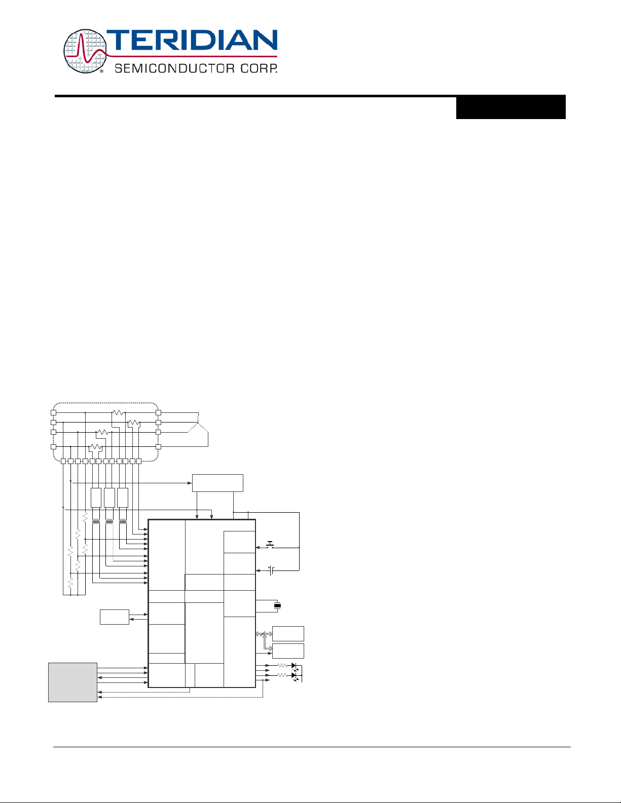
Figure 1: IC Functional Block Diagram
v1.0 © 2008–2011 Teridian Semiconductor Corporation 9

Data Sheet 71M6545/H PDS_6545_009
1 INTRODUCTION
This data sheet covers the 71M6545 (0.5%) and 71M6545H (0.1%) fourth generation Teridian poly-phase
Metrology Processors. The term “71M6545/H” is used when discussing a dev ice feature or behavi or that
is applicable to bot h par t number s. The appropriate part number is indicated when a device feature or
behavior is bei ng discussed that applies only to a specific part num ber. This data sheet also covers
details about the com panion 71M6xx3 isolated current sensor dev ice.
This document covers the use of the 71M6545/H in conjunc tion with the 71M6xx3 isolated cur r ent sensor.
The 71M6545/H and 71M6xx3 ICs make it possible to use one non-isolated and thr ee additional isolated
shunt current sensors to c r eate poly-phase energy meters using inexpensive shunt resistors, while
achieving unpr ec edented performance with this type of sensor technol ogy . The 71M6545/H Metrology
Processors also support Cur r ent Transformers (CT).
To facilitat e doc um ent navigation, hyperlinks are often used to reference figures, tables and secti on
headings that are l oc ated in other parts of the document. All hyperlink s i n this document are highlighted in
blue. Hyperlinks are used extensively to increase the level of detail and clarity prov ided within each
section by refer enci ng other relevant parts of the document. To further facilitate document nav igation, this
document is published as a PDF docum ent with bookmarks enabled.
The reader is also encouraged to obt ain and review the document s listed i n 8 RELATED
INFORMATION on page 132 of t his document.
10 © 2008–2011 Teridian Semiconductor Corporation v1.0

PDS_6545_009 Data Sheet 71M6545/H
2 HARDWARE DESCRIPTION
2.1 Hardware Overview
The Teridian 71M6545/H single-chip Metrology Processor integrates all primary functional blocks required
to implement a solid-state electricity meter. Included on the c hip ar e:
• An analog front end (AFE) featuring a 22-bit second-order sigma-delta ADC
• An independent 32-bit digital computation engine (CE) to implement DSP functions
• An 8051-compati ble mi c r opr oc essor (MPU) whic h ex ecutes one i nstruc tion per clock cycle (80515)
• A precision v oltage reference (VREF)
• A temperature sensor for digital temperature com pensation:
- Metrology digital temperature compensati on ( MPU)
- Automatic RTC digital temperature compensation operational in sleep mode (SLP)
• RAM and Flash memory
• A real time clock (RTC)
• A variety of I/O pins
• A power failure interr upt (CE code feature)
• A zero-crossing interrupt (CE code feature)
• Selectable c ur r ent sensor interfaces for locally-connected sensors as well as isolated sensors (i.e.,
using the 71M6xx3 companion IC with a shunt resistor senso r)
• Resistive Shunt and Current Transf ormers are supported
In order to implement a poly-phase meter with or without neutral curr ent sensing, one resistive shunt
current sensor may be c onnec ted directly (non-isolated) to the 71M6545/H device, while three additional
current shunts are isolated using a companion 71M6xx3 i sol ated sensor IC. An inexpensive, small si z e
pulse transform er is used to electrically isolate the 71M6xx3 remote sensor from the 71M6545/H. The
71M6545/H performs digital communications bi-dir ec tionally with the 71M6xx3 and also provides power to
the 71M6xx3 through the isolating pulse transform er . I sol ated (remote) shunt current sensors are
connected to the diff er ential input of the 71M6xx3. The 71M6545/H may also be used with Current
Transformer s; in this case the 71M6xx3 isolated sensors are not required. Included on the 71M6xx3
companion isol ator chip are:
• Digital isol ation communications interf ac e
• An analog front end (AFE) featuring a 22-bit second-order sigm a-delta ADC
• A precision voltage reference (VREF)
• A temperature sensor (for current-sensing digital temperature compensation)
• A fully differ ential shunt resistor sensor input
• A pre-amplifier to optimize shunt current sensor performance
• Isolated power circ uitry obtains dc power from pulses sent by the 71M6545/H
In a typical appli c ation, the 32-bit compute engine (CE) of the 71M6545/H sequentially processes the
samples from the voltage inputs on analog input pins and performs calculations to m easure active energy
(Wh) and reactive energy (VARh), as well as A
are then accessed by the host processor via the SPI or by the on-chip MPU, to be processed further and
output using either the peripheral devices available to the on-chip MPU or by the host processor.
In addition to ad vanced measurement funct ions , the rea l time cloc k (RTC) function allows the 71M6545/H to
record time of use (TOU) metering information for mu lti-rate applications an d to time-stamp tamper or other
events. An automatic RTC temperature compensation circuit operates in all power states including when the
MPU is halted, and continues to compensate using back-up battery power during power outages
(VBAT_RTC pin).
2
h, and V2h for four-quadrant metering. These measurements
In addition to the temperature-trimmed ultra-pr eci si on vol tage reference, the on-chip digital temperature
compensation mechanism includes a temperature sensor and associated controls for correction of unwanted
temperature effects on metrology and RTC accuracy (i.e., to meet the requirements of ANSI and IEC
standards). Temperature-dependent external components such as the crystal, current transformers
(CTs), Current Shunts and the ir corres pond ing signal conditioning cir cu its can be ch ara c terized and their
v1.0 © 2008–2011 Teridian Semiconductor Corporation 11
Data Sheet 71M6545/H PDS_6545_009
∆Σ ADC
CONVERTER
VREF
MUX
VREF
VREF
VADC
22
FIR
IADC2
VADC9 (VB)
IADC0
VADC8 (VA)
IADC1
IADC3
71M6545/H
CE RAM
71M6xx3
SP
SN
INP
INN
Remote
Shunt
IB
Digital
Isolation
Interface
Local
Shunt
IN*
22
IADC4
IADC5
71M6xx3
SP
SN
INP
INN
Remote
Shunt
IC
VADC10 (VC)
22
IADC6
IADC7
71M6xx3
SP
SN
INP
INN
Remote
Shunt
IA
22
*IN = Neutral Current
10/7/2010
correction factors can be pro grammed to produce electricity meters with exceptional accuracy over the
industrial temperature range.
One of the two internal UARTs is adapted to support an Infrared LED with internal drive and sense
configuration and c an also function as a standard UART. This flexibility makes it possible to implement
AMR meters with an IR interface. A block diagr am of the IC is shown in Figure 1.
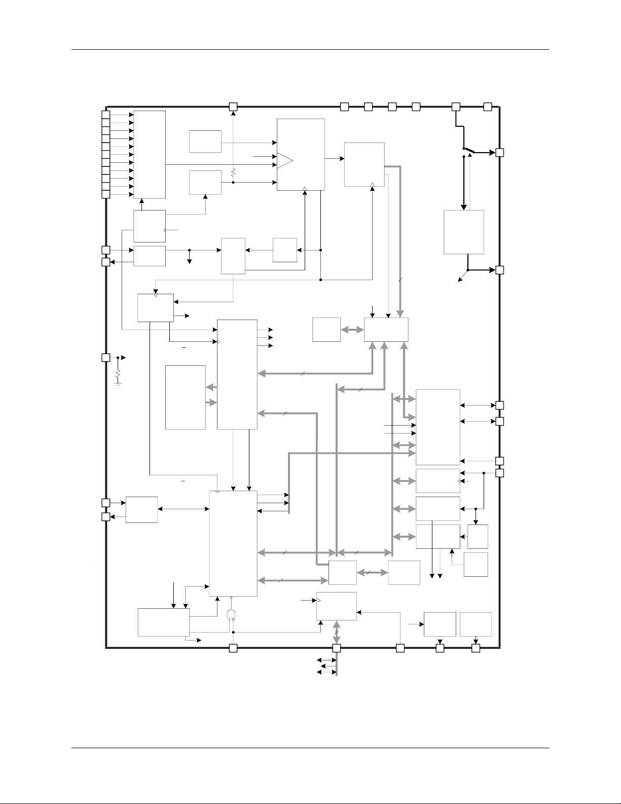
2.2 Analog Front End (AFE)
The AFE functions as a data acquisition system, control led by the MPU or by the host processor over the
SPI interface. The 71M6545/H AFE may also be augmented by isolated 71M6xx3 sensors in order t o
support low-cost current shunt sensors. Figure 2 and Figure 3 show two of the most common
configurati ons; other configurations are possible. Sensors that are connect ed dir ec tly to the 71M6545/H
(i.e., IADC0-IADC1, VADC8, VADC9 and VADC10) are multiplexed into the single second-order sigmadelta ADC input for sampling in the 71M6545/H. The 71M6545/H ADC output is decimated by the FIR
filter and stored i n CE RAM where it c an be accessed and proces sed by t he CE .
Shunt current sensors that are isolated by using a 71M6xx3 device, are sampled by a second-order
sigma delta ADC in the 71M6xx3 and t he si gnal samples are transferred over the digital isolation interface
through the low-cost isolation pulse transf ormer.
Figure 2 shows the 71M6545/H using shunt cur r ent sensors and the 71M6xx3 isolated sensor dev ices.
Figure 2 supports neutral c ur r ent measurement with a local shunt connected to the IADC0-IADC1 input
plus three remote (i sol ated) shunt sensors. As seen in Figure 2, when a remote isolated shunt sen sor is
connected via the 71M6xx3, the sam ples associ ated with this current channel ar e not routed to the
multiplexer, and are instead transferred digitally to the 71M6545/H via the isolati on interface and are
directly stor ed in CE RAM. The MUX_SELn[3:0] I/O RAM control fields allow the MPU to configur e the
AFE for the desired multiplexer sampling sequence. Refer to Table 1 and Table 2 for the appropriate CE
code and the corresponding AFE settings.
See Figure 27 f or the m eter wiri ng c onfiguration corresponding to Figure 2.
12 © 2008–2011 Teridian Semiconductor Corporation v1.0
Figure 2: AFE Block Diagram (Shunts: One-Local, Three-Remotes)
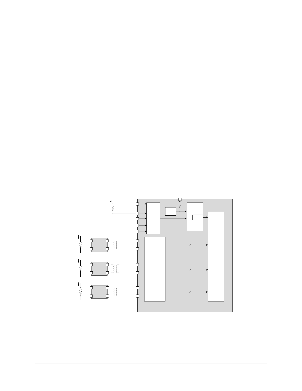
PDS_6545_009 Data Sheet 71M6545/H
∆Σ ADC
CONVERTER
VREF
MUX
VREF
VREF
VADC
22
FIR
IADC4
VADC9 (VB)
IADC2
VADC8 (VA)
IADC3
IADC5
71M6545/H
CE RAM
IB
CT
IA
CT
IADC6
IADC7
IC
CT
IADC0
IADC1
IN*
CT
VADC10 (VC)
10/7/2010
*IN = Neutral Current
The 71M6545/H AFE c an also be di r ectly interfaced to Current Transformers (CTs), as seen in Figure 3.
In this case, all volt age and c ur r ent channels are multiplexed int o a si ngle second-order si gma-delta ADC
in the 71M6545/H and the 71M 6xx3 remote isolated sensors are not used. The four th CT and the
measurement of Neutral c ur r ent via the IADC0-IADC1 current channel are optional.
See Figure 28 f or the m eter wiri ng c onfiguration corresponding to Figure 3.
Figure 3. AFE Block Diagram (Four CTs)
2.2.1 Signal Input Pins
The 71M6545/H features eleven ADC input pins.
IADC0 through IADC7 are intended for use as current sensor inputs. These eight current sensor inputs can
be configured as e ight s ingle-ended inputs, or can be paired to form four diffe ren tial inputs. For best
performance , it is reco m men ded to con figure the cu rrent sensor inputs as dif feren t ia l inputs (i.e., IADC0IADC1, IADC2-IADC3, IADC4-IADC5 and IADC6-IADC7). The first differential input (IADC0-IADC1)
features a pre-amplifier with a selectable gain of 1 or 8, and is intended for direct connect ion to a sh unt
resistor sensor , and can also be used with a Current Transformer (CT). The three remaining differential
pairs (i.e., IADC2 -IADC3, IADC4-IADC5 and IADC6-IADC7) may be used with CTs, or may be enabled to
interface to a remote 71M 6xx3 isolated cu r rent sensor pr oviding isolation for a shunt resistor sensor us ing a
low cost pulse transformer.
The remaining three inputs VADC8 (VA) , VADC9 (VB) and VADC10 (VC) are single-ended, and are
intended for sensing each of the phase voltages in a poly-phas e meter application. These three singleended inputs are referenced to the V3P3A pin.
All ADC input pins measure voltage. In the case of shunt current sensors, currents are sensed as a voltage
drop in the shunt resis tor sens o r. In the cas e of Cu r ren t T ransformers (CT), the curr en t is measu red as a
voltage across a burden resis to r tha t is conn ec ted to th e s econda r y o f the C T. Meanwhile, line voltages are
sensed through resistive voltage di viders. The VADC8 (VA), VADC9 (VB) and VADC10 (VC) pins are
single-ended and their common return is the V3P3A pin. See Figure 23, Figure 24, Figure 25 and Figure
26 for detail ed connect ions for each type of sensor.
Pins IADC0-IADC1 can be programmed individuall y to be differential or single-ended as determined by
the DIFF0_E (I/O RAM 0x210C[4]) control bit. However, for most applications, IADC0-IADC1 are
v1.0 © 2008–2011 Teridian Semiconductor Corporation 13

Data Sheet 71M6545/H PDS_6545_009
configured as a diff er ential input to work with a resistive shunt or CT directly i nterfaced to the IADC0-
IADC1 diff erential input with the appropriate external signal conditioning components.
The performance of t he IADC0-IADC1 pins can be enhanced by enabling a pre-amplifier with a fixed gain
of 8, using the I/O RAM control bit PRE_E (I/O RAM 0x2704[5]). When PRE_E = 1, IADC0-IADC1 become
the inputs to the 8x pre-am plifier, and the output of this amplifier is supplied to the multiplexer. The 8x
amplificati on is usef ul when current sensors with low sensitivity, such as shunt resistors, are used. With
PRE_E set, the IADC0-IADC1 input signal amplitude is restricted t o 31.25 mV peak. When PRE_E = 0
(Gain = 1), the IADC0-IADC1 input signal is restricted to 250 mV peak.
For the 71M6545/H application utilizing shunt resistor sensors (Figure 2), the IADC0-IADC1 pins are
configured for differential mode to interface to a local shunt by setting the DIFF0_E control bit. Meanwhile,
the IADC2-IADC3 , IADC4-IADC5 and IADC6-IADC7 pins are re-configure d as digital remot e s ensor
interface designed to c ommunicate with a Teridian 71M6xx3 isolated sensor by setting the RMTx_E control
bits (I/O RAM 0x2709[ 5:3]). The 71M6xx3 communicates with the 71M6545/H using a bi-directional digital
data stream thro ugh an isolating low-cost pulse transformer. The 71M6545/H also supplies power to the
71M6xx3 through the isolating t ransformer. This type of interface is further descr ibed at the end of this
chapter. See 2.2.8 71M6xx3 Isolated Sensor Interface.
For use with Current Transformer s (CT s), as shown in Figure 3, the RMTx_E control bits are reset, so that
IADC2-IADC3, IADC4-IADC5 and IADC6-IADC7 are confi gur ed as local analog inputs. The IADC0-IADC1
pins cannot be configured as a remote sensor interface.
2.2.2 Input Mu lt ip le x e r
When operating with locally connected sensors, the input multiplexer sequentially applies the input signals
from the analog input pins to the input of the ADC (see Figure 3), according to the sampling sequence
determined by the eleven MUXn_SEL[3:0] control fields. One complete sampling sequence is called a
multiplexer frame. The multiplexer of the 71M6545/H can select up to eleven input signals when the current
senso r inputs are configured for single-ended mode. When the current sensor inputs are configured in
differential mode (recommended for best performance), the number of input signals is seven (i.e., IADC0IADC1, IADC2-IADC3, IADC4-IADC5, IADC6-IADC7, VADC8, VADC9 and VADC10) per multiplexer frame.
The number of slots in the multiplexer frame is controlled by the I/O RAM control field MUX_DIV[3:0] (I/O
RAM 0x2100[7:4]) (see Figure 4). T he multi plex er al ways st ar t s at stat e 0 and proceeds unt il the num ber
of sensor channels determined by the MUX_DIV[3:0] field sett i ng have been converted.
The 71M6545/H requires a unique CE code that is written f or the sp ec ific meter configurat ion.
Moreover, eac h CE code requires speci fic AFE and MUX settings in or der to functio n properly. Table 1
provides the C E c ode and s ettings correspondi ng to the 1-Local / 3-Remote sen sor co nf i gur ati on
shown in Figure 2. Table 2 provides the CE code and settings correspondi ng to the CT configuration
shown in Figure 3
.
14 © 2008–2011 Teridian Semiconductor Corporation v1.0

PDS_6545_009 Data Sheet 71M6545/H
I/O RAM
Mnemonic
I/O RAM
Location
FIR_LEN[1:0]
210C[2:1] 1 288 cycles
ADC_DIV
2200[5]
0
Fast
PLL_FAST
2200[4] 1 19.66 MHz
MUX_DIV[3:0]
2100[7:4] 6 See note 1
MUX0_SEL[3:0]
2105[3:0]
0
Slot 0 is IADC0-IADC1
(IN)
MUX1_SEL[3:0]
2105[7:4] 1 Unused (See note 2)
MUX2_SEL[3:0]
2104[3:0] 1 Unused (See note 2)
MUX3_SEL[3:0]
2104[7:4]
8
Slot 3 is VADC8
(VA)
MUX4_SEL[3:0]
2103[3:0]
9
Slot 4 is VADC9
(VB)
MUX5_SEL[3:0]
2103[7:4]
A
Slot 5 is VADC10
(VC)
MUX6_SEL[3:0]
2102[3:0]
0
MUX7_SEL[3:0]
2102[7:4]
0
MUX8_SEL[3:0]
2101[3:0]
0
MUX9_SEL[3:0]
2101[7:4]
0
MUX10_SEL[3:0]
2100[3:0]
0
RMT2_E
2709[3]
1
Enable Remote IADC2-IADC3
(IA)
RMT4_E
2709[4]
1
Enable Remote IADC4-IADC5
(IB)
RMT6_E
2709[5]
1
Enable Remote IADC6-IADC7
(IC)
DIFF0_E
210C[4]
1
Differential IADC0-IADC1
(IN)
DIFF2_E
210C[5] 0 See note 3
DIFF4_E
210C[6] 0 See note 3
DIFF6_E
210C[7] 0 See note 3
PRE_E
2704[5] 1 IADC0-IADC1 Gain = 8
EQU[2:0]
2106[7:5]
5
IA*VA + IB*VB + IC*VC
ce43b016603 (use with 71M 6603)
ce43b016203 (use with 71M 6203)
Equation(s)
5
Current Sensor Type
1 Local Shunt and 3 Remote Shunts
Applicable Figures
Figure 2 and Figure 27
Notes:
representative to obtain the latest CE code and the associat ed settings.
Table 1. Required CE Code and Settings for 1-Local / 3-Remotes
I/O RAM Setting Comments
Slots not enabl ed
CE Codes
(See note 4)
ce43b016103 (use with 71M 6103)
ce43b016113 (use with 71M 6113)
1. MUX_DIV[3:0] should be set to 0 while writing the other v alues i n this table, and then set
to the indicated v alue before writing the MUXn_SEL[3:0] fields.
2. Each unused slot m ust be assigned to a valid (0 to A), but unused ADC handle
3. This channel is remote (71M6xx3), hence DIFFx_E is irrelev ant
4. Must use the CE code that corresponds to the specific 71M6xx3 device used
TERIDIAN updates the CE c ode peri odically. Please contact your local TERIDIAN
v1.0 © 2008–2011 Teridian Semiconductor Corporation 15

Data Sheet 71M6545/H PDS_6545_009
I/O RAM
Mnemonic
I/O RAM
Location
I/O RAM Setting
(Hex)
FIR_LEN[1:0]
210C[2:1] 1 288 cycles
ADC_DIV
2200[5]
0
Fast
PLL_FAST
2200[4] 1 19.66 MHz
MUX_DIV[3:0]
2100[7:4] 7 See note 1
MUX0_SEL[3:0]
2105[3:0]
2
Slot 0 is IADC2-IADC3
(IA)
MUX1_SEL[3:0]
2105[7:4]
8
Slot 1 is VADC8
(VA)
MUX2_SEL[3:0]
2104[3:0]
4
Slot 2 is IADC4-IADC5
(IB)
MUX3_SEL[3:0]
2104[7:4]
9
Slot 3 is VADC9
(VB)
MUX4_SEL[3:0]
2103[3:0]
6
Slot 4 is IADC6-IADC7
MUX5_SEL[3:0]
2103[7:4]
A
Slot 5 is VADC10
(VC)
MUX6_SEL[3:0]
2102[3:0] 0 Slot 6 is IADC0-IADC1
(IN – See note 2)
MUX7_SEL[3:0]
2102[7:4]
0
MUX8_SEL[3:0]
2101[3:0]
0
MUX9_SEL[3:0]
2101[7:4]
0
MUX10_SEL[3:0]
2100[3:0]
0
RMT2_E
2709[3]
0
Local Sensor IADC2-IADC3
RMT4_E
2709[4]
0
Local Sensor IADC4-IADC5
RMT6_E
2709[5]
0
Local Sensor IADC6-IADC7
DIFF0_E
210C[4] 1 Differential IADC0-IADC1
DIFF2_E
210C[5] 1 Differential IADC2-IADC3
DIFF4_E
210C[6] 1 Differential IADC4-IADC5
DIFF6_E
210C[7] 1 Differential IADC6-IADC7
PRE_E
2704[5] 0 IADC0-IADC1 Gain = 1
EQU[2:0]
2106[7:5] 5 IA*VA + IB*VB + IC*VC
CE Code
ce43a02
Equation(s)
5
Current Sensor Type
4 Current Transform er s (CT s)
Applicable Figures
Figure 3 and Figure 28
Notes:
to obtain the latest CE code and t he associated settings.
Table 2. Required CE Code and Settings for CT Sensors
Comments
(IC)
Slots not enabl ed
1. MUX_DIV[3:0] should be set to 0 while writing the other v alues i n this table, and then set to
the indicated value before writing the MUXn_SEL[3:0] fields.
2. IN is the optional Neutral Current
TERIDIAN updates the CE c ode peri odically. Please contact your loc al TERIDIAN representative
Using settings for t he I/O RAM Mnemonics li sted in Table 1 and Table 2 that do not match
those requir ed by the corres pondin g CE code being used may result in unde si ra bl e sid e
effects and must not be selected by the MPU. Consult your l ocal TERIDIAN representative to
obtain the correct CE code and AFE / M UX settings corresponding t o the applicati on.
For a poly-phase configur ation with neutral current sensing using shunt r esi stor c ur r ent sensors and the
71M6xx3 isolated sensors, as shown in Figure 2, the IADC0-IADC1 input must be configured as a
differential input, to be connected to a local shunt (see Figure 26 for the shunt connection details). The
local shunt connected to the IADC0-IADC1 input is used to sense the Neutral current. The voltage
senso rs (VADC8, VADC9 and VADC10) are also dir ectly connected to the 71M6545/H (see Figure 23 for
16 © 2008–2011 Teridian Semiconductor Corporation v1.0

PDS_6545_009 Data Sheet 71M6545/H
CK32
MUX STATE 0 1 2 3 4
5
MUX_DIV[3:0] = 6 Conversions
Settle
Multiplexer Frame
S
CROSS
MUX_SYNC
S
IN
Unused
Unused VA VB VC
1 Local / 3 Remotes:
CK32
MUX STATE 0 1 2 3 4
5
MUX_DIV[3:0] = 7 Conversions
Settle
Multiplexer Frame
S
CROSS
MUX_SYNC
S
6
IA
VA
IB VB
IC VC IN
the connecti on details) and are also routed though t he multiplex er , as seen in Figure 2. Meanwhile, the
IADC2-IADC3, IADC4-IADC5 and IADC6-IADC7 current inputs are configured as remote sensor digital
interfac es and the c or r espondi ng samples are not routed through the multi plex er. For this configuration,
the multiplex er sequence is as shown in Figure 4.
For a poly-phase configur ation with optional neutral current sensing u si ng Cur r ent Transformer (CTs)
sensors, as shown in Figure 3, all four current sensor inputs must be configur ed as a differential inputs,
to be connected to their c or r espondi ng CTs (see Figure 25 for the differential CT connection details). The
IADC0-IADC1 curr ent sensor input is optionally used to sense the Neutr al current for anti-tampering
purposes. The voltage sensors (VADC8, VADC9 and VADC10) are directly connec ted to the 71M6545/H
(see Figure 23 for the voltage sensor connection details). No 71M 6x x3 isolated sensors are used in this
configurati on and all sensors are routed through the multiplexer, as seen in Figure 3. For this
configurati on, the multiplexer sequence is as shown in Figure 5.
The multiplex er sequence sho wn in Figure 4, covers the shunt configur ation shown in Figure 2. The
frame duration is 13 CK32 cycl es (where CK32 = 32,768 Hz ) , therefore, the resulting sam ple r ate is
32,768 Hz / 13 = 2,520.6 Hz. Note that Figure 4 only shows the currents that pass through t he
71M6545/H multiplexer, and does not show the currents that are c opied directly into CE RAM from the
remote sensors (see Figure 2), which are sampled during the second half of the multiplexer frame. The
two unused conver si on sl ots shown are necessary to produce the desired 2,520.6 Hz sample rate.
Figure 4: States in a Multiplexer Frame (MUX_DIV[3:0] = 6)
The multiplex er sequence sho wn in Figure 5 corresponds to the CT configurat ion shown in Figure 3.
Since in this case all current sensors are locally c onnected to the 71M6545/H, all currents are routed
through the multiplexer, as seen in Figure 3. For this multiplex er sequence, t he frame duration is 15 CK32
cycles (where CK32 = 32, 768 Hz ), theref or e, the resulting sample rate is 32,768 Hz / 15 = 2,184.5 Hz.
Figure 5: States in a Multiplexer Frame (MUX_DIV[3:0] = 7)
Multiplexer adv anc e, FIR initiation and chopping of the ADC reference voltage (using the internal CROSS
signal, see 2.2.7 Voltage References) are contr olled by the internal MUX_CTRL circuit. Additionally,
MUX_CTRL launches each pass of the CE through its c ode. Conceptually, MUX_CTRL is clocked by
CK32, the 32768 Hz c lock from the PLL block. The behavior of the MUX_CTRL circuit is governed by:
v1.0 © 2008–2011 Teridian Semiconductor Corporation 17

Data Sheet 71M6545/H PDS_6545_009
• CHOP_E[1:0] (I/O RAM 0x2106 [3 :2])
• MUX_DIV[3:0] (I/O RAM 0x2100[7:4])
• FIR_LEN[1:0] (I/O RAM 0x210C[2:1])
• ADC_DIV (I/O RAM 0x2200[5])
The duration of each multiplexer state depends on the number of ADC samples processed by the FIR as
determined by the FIR_LEN[1:0] (I/O RAM 0x210C[2:1] control field. Each multiplexer state star ts on the
rising edge of CK32, t he 32-kHz clock.
It is r ecommended that MUX_DIV[ 3:0] (I/O RAM 0x2200[2:0]) b e set to z ero while changing the ADC
confi guratio n. Alth ough not required, it minimizes syste m t ra nsients that might be caused by momentary
shorts between the AD C inpu ts, especiall y when changing t he DIFFn_E cont rol bits (I/O RAM 0x210C[5:4 ]).
After the configuration bit s are set, MUX_DIV[3:0] should be set to the requir ed value.
The duration of each time sl ot in CK32 cycles depends on FIR_LEN[1:0], ADC_DIV and PLL_FAST:
Time_Slot _Dur ation (PLL_FAST = 1) = (FIR_LEN[1:0]+1) * (ADC_DIV+1)
Time_Slot _Dur ation (PLL_FAST = 0) = 3*(FIR_LEN[1:0]+1) * (ADC_DIV+1)
The duration of a multiplex er fram e in CK32 c ycles is:
MUX_Frame_Durati on = 3-2*PLL_FAST + Tim e_Sl ot_Duration * MUX_DIV[3:0]
The duration of a multiplexer frame in CK_FI R cycle s is:
MUX frame duration (CK_FI R c ycles) =
[3-2*PLL_FAST + Time_Slot_Dur ation * MUX_DIV] * (48+PLL_FAST*102)
The ADC conv er si on sequence is programmabl e throug h the MUXn_SEL control fields (I/O RAM 0x 2100
to 0x2105). As stated above, there are up to eleven ADC time slot s in the 71M6545/H, as set by
MUX_DIV[3:0] (I/O RAM 0x2100[7:4]). In the expression MUXn_SEL[3:0] = x, ‘ n’ refers to the multiplexer
frame time slot number and ‘x’ refers to the desired ADC input number or ADC handle (i.e., IADC0 to VADC10,
or simply 0 to 10 decimal). Thus, there are a total of 11 valid ADC handles in the 71M6545/H devices. For
example, if MUX0_SEL[3:0] = 0, then IADC0, corresponding to the sample from the IADC0-IADC1 input
(configured as a differential input), is posit io ned in the multiplexer frame during time slot 0. See Table 1 and
Table 2 for the appr opr iate MUXn_SEL[3:0] settings and other settings applicable to a particular meter
confi gur ati o n and CE code.
Note that when the remote sensor interface is enabled, the samples corr esponding to the remot e
sensor currents do not pass through the 71M6545/H multiplexer. The sampling of the remote current
sensors occurs in the s econd half of the multiplexer frame. The VA , VB and VC voltages ar e assigned
the las t three slots in the frame. With this slot assignm ent for VA, VB and V C, the sam pli ng of the
corresponding remote sensor currents bear s a precis e timing relatio nship to their corresp onding phase
volt ages, a nd delay compe n sati on i s acc ur atel y pe rform ed (see 2.2.3 Delay Compensation on page 19).
Also when using remote sensors, it is neces s ary to introd uce unused slots to realize the numb er of
slot s specified by the MUX_DIV[3:0] (I/O RAM 0x2100[7:4]) fiel d setting (see
MUXn_SEL[3:0] control fiel ds for these unused (“dummy”) slots must be writt en with a valid ADC handle
(i.e., 0 to 10 decimal) that is not otherwise being used. In thi s manner, the unused ADC handle, i s used
as a “dummy” place holder in t he multiplex er frame, and the cor re ct duration multiplexer frame
sequence is gene rated and also the desired sample rate. The result ing sample dat a stored in the CE
RAM loc ation corresponding to the “ dummy” A DC handl e is ignored by the CE code. Me anwhile, the
digital isolation interface takes care of automatically st or ing the samples for th e remote current sensors
in the appropriate CE RAM locations.
Figure 4 and Figure 5). The
Delay compensati on and other functions in the CE code require t he settings for MUX_DIV[3:0],
MUXn_SEL[3:0], RMT_E, FIR_L EN [1:0 ], ADC_DIV and PLL_FAST to be fix ed for a given CE code.
Refer to Table 1 and Table 2 for the settings that are applic able to the 71M6545/H.
18 © 2008–2011 Teridian Semiconductor Corporation v1.0

PDS_6545_009 Data Sheet 71M6545/H
MUX5_SEL[3:0]
MUX7_SEL[3:0]
2102[7:0]
Selects the AD C input converted duri ng time slot 7.
ADC_DIV
Controls the rate of the ADC and FIR clocks.
2100[7:4]
The number of ADC time slots in each multiplexer frame (maximum = 11 ).
Determines the number of ADC cycles in the AD C decimation FIR f i lter .
DIFF0_E
o
delay
o
delay
ft
T
t
360360 ⋅⋅=⋅=
φ
Table 3 summarizes the I/ O RAM registers used for configuring the m ultiplexer, signals pins , and ADC .
All listed registers are 0 after reset and wake from SLP mode, and are reada ble and writable.
Table 3: Multiplexer and ADC Configuration Bits
Name Location Description
MUX0_SEL[3:0] 2105[3:0] Selects the ADC input converted duri ng time slot 0.
MUX1_SEL[3:0] 2105[7:4] Selects the ADC input converted duri ng time slot 1.
MUX2_SEL[3:0] 2104[3:0] Selects the ADC input converted duri ng time slot 2.
MUX3_SEL[3:0] 2104[7:4] Selects the ADC input converted duri ng time slot 3.
MUX4_SEL[3:0] 2103[3:0] Selects the ADC input converted duri ng time slot 4.
2103[7:4] S elects the ADC i nput converted during time slot 5.
MUX6_SEL[3:0] 2102[3:0] Selects the ADC input converted duri ng time slot 6.
MUX8_SEL[3:0] 2101[3:0] Selects the ADC input converted duri ng time slot 8.
MUX9_SEL[3:0] 2101[7:0] Selects the ADC input converted during time slo t 9.
MUX10_SEL[3:0] 2100[3:0] Select s the ADC in put convert ed during ti me slot 10.
2200[5]
MUX_DIV[3:0]
PLL_FAST 2200[4]
FIR_LEN[1:0]
DIFF2_E 210C[5] Enables the differential configuration for analog input pins IADC2-IADC3 .
DIFF4_E 210C[6] Enables the differential configuration for analog input pins IADC4-IADC5 .
DIFF6_E 210C[7] Enables the differential configuration for analog input pins IADC6-IADC7 .
RMT2_E 2709[3]
RMT4_E 2709[4]
RMT6_E 2709[5]
PRE_E 2704[5] Enables the 8x pre-amplifier.
Refer to Table 61 starting on page 88 for mor e complete detai l s about thes e I/O R AM loca t ions .
210C[2:1]
210C[4] Enables the differential configuration for analog input pins IADC0-IADC1 .
Controls the speed of the PLL and MCK.
Enables the remote sensor interface transforming pin s IADC2-IADC3 into a digital
interface for communications with a 71M6xx3 sensor.
Enables the remote sensor interface transforming pin s IADC4-IADC5 into a digital
interface for communications with a 71M6xx3 sensor.
Enables the remote sensor interface transforming pin s IADC6-IADC7 into a digital
interface for communications with a 71M6xx3 sensor.
2.2.3 Delay Compensation
When measuring the energy of a phase (i .e., Wh and VARh) in a service, the voltage and c ur r ent f or that
phase must be sampled at the same instant . Otherwise, the phase diff er enc e, Ф, introduces errors.
Where f is the frequency of the input signal, T = 1/f and t
voltage.
Traditionally, sampling is accomplished by using t wo A/D c onverters per phase (one for volt age and the
other one for curr ent) c ontrolled to sample simultaneously. Teridian’s Single-Converter Technology
however, exploits the 32-bit signal processing capability of its CE to implement “constant delay” all-pass
filters. The all-pass filt er corr ec ts for the conversion time difference between the voltage and the
corresponding current samples that are obtained with a single multiplexed A/D convert er .
The “constant del ay ” all -pass fi lter provides a broad-band delay 360
difference i n sample time between the voltage and the current of a giv en phase. This digital filter does
not affect the ampli tude of the signal, but provides a precisel y c ontrolled phase response.
The recommended ADC multiplexer sequence samples the curr ent fi r st, immediately followed by
sampling of the corr espondi ng phase voltage, thus the volt age is del ay ed by a phase angle Ф relative to
the current. The delay c om pensation implemented in the CE aligns the v oltage samples with their
corresponding current samples by first delaying the current samples by one full sample interval (i. e.,
v1.0 © 2008–2011 Teridian Semiconductor Corporation 19
is the sampling delay between current and
delay
o
- θ, that is precisely matched t o the
®
,

Data Sheet 71M6545/H PDS_6545_009
360o), then routing the voltage samples through the all-pass filter, thus delaying the voltage samples by
o
360
- θ, resulting in the residual phase error between the curr ent and its corresponding volt age of θ – Ф.
The residual phase error is negligible, and is typic ally less than ±1.5 mil li-degrees at 100Hz, thus it does
not contribute to errors in the energy measurements.
When using remote sensors, t he CE performs the same delay compensation described above to align
each voltage sample with its corresponding current sample. Even though the remote current sam ples do
not pass through the 71M6545/H multiplexer, their timing rel ationship to their corresponding voltages is
fixed and precisel y known, provided that the MUXn_SEL[3:0] slot assignment fields are progr ammed as
shown in Table 1. Note that these slot assignments result in VA, VB and VC occupying m ultiplexer slots
3, 4 and 5, respectively ( see Figure 4).
2.2.4 ADC Pre-Amplifier
The ADC pre-amplifier is a low-noise differential amplifier with a fix ed gain of 8 av ailable only on the
IADC0-IADC1 sensor input pins. A gain of 8 is enabled by setti ng PRE_E = 1 (I/O RAM 0x2704[5]). When
disabled, the suppl y c ur r ent of the pr e-amplifier is <10 nA and the gain is unity. With proper settings of
the PRE_E and DIFF0_E (I/O RA M 0x 210C[4]) bits, the pre-amplifier can be used whether differential
mode is selected or not. For best performance, the differential m ode is recommended. In order to save
power, the bias current of the pre-amplifier and ADC is adjus ted ac co rd ing to the ADC_DIV control bit (I/O
RAM 0x2200[5]).
2.2.5 A/D Converter (ADC)
A single 2nd order sigma-delta A/D converter digitizes the voltage and current inputs to the dev ic e. The
resolution of the ADC, including the sign bit, is 21 bits (FIR_LEN[1:0] = 01, I/O RAM 0x210C[2:1]), or 22
bits (FIR_LEN[1:0] = 10). The ADC is clocked by CKADC.
Initiati on of each A DC conversion is controlled by the internal MUX_CTRL circuit as described earlier. At
the end of each ADC conversion, the FIR filter output data is stored into the CE RAM location determined by
the multiplexer selection.
2.2.6 FIR Fi lter
The finite impulse response filter is an integral part of the ADC and it is optimized for use with the multiplexer.
The purpose of the FIR filter is to decimate the ADC output to the desired resolution. At the end of each
ADC conversion, t he output data is stored into the fixed CE RAM location det ermined by the multiplexer
selection stor ed in the MUXn_SEL[3:0] fields. FIR data is stored LSB-justified, but shifted left by 9 bits.
2.2.7 Voltage References
A bandgap circuit provides the reference voltage to the ADC . The amplifier within the reference is chopper
stabilized, i.e., the chopper circ uit can be enabled or disabled by the MPU using the I/O RAM control field
CHOP_E[1:0] (I/O RAM 0x2106[3:2]). The two bits in the CHOP_E[1:0] field enable the MPU to operate the
chopper circuit in regular or inverte d operation, or in toggling modes (recommended). When the
chopper circ uit is t oggled i n between multiplexer cycles, dc offsets on VREF are automatically averaged
out, theref or e the chopper ci r c uit should always be configured for one of the toggling modes.
Since the VREF band -gap amplifier is chopper-stabilized, the dc off set v oltage, which is the most
significant long-term drift mechanism in the voltage references (VREF), is automatic ally r em ov ed by the
chopper circuit. B oth the 71M6545/H and the 71M6xx3 feature chopper ci r c uits for their respective VREF
voltage ref er enc e.
The general topology of a chopped am plifier is shown in Figure 6. The CROSS signal is an inter nal onchip signal and is not accessibl e on any pin or register.
20 © 2008–2011 Teridian Semiconductor Corporation v1.0
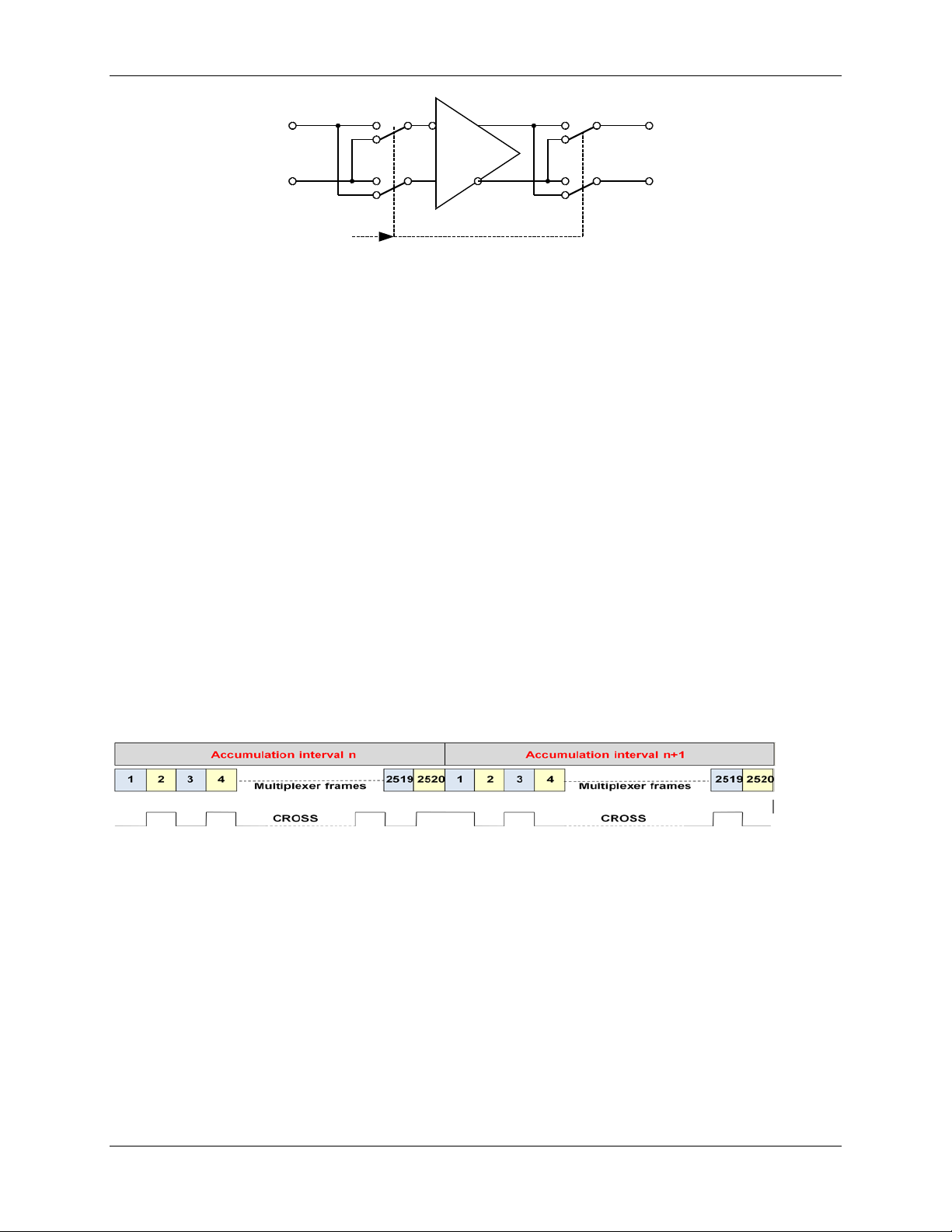
PDS_6545_009 Data Sheet 71M6545/H
G
-
+V
inp
V
outp
V
outn
V
inn
CROSS
A
B
A
B
A
B
A
B
Figure 6: General Topology of a Chopped Amplifier
It is as s umed th at an offset voltage Voff appears at the posi tiv e amplifier input. With all switches, as
controlled by CRO S S ( an internal signal), in the A position, the output voltage is:
Voutp – Voutn = G (Vinp + Voff – Vinn) = G (Vinp – Vinn) + G Voff
With all switches set to the B posi tion by applying the inverted CROSS signal, the output voltage is:
Voutn – Voutp = G (Vinn – Vinp + Voff) = G (Vinn – Vinp) + G Voff, or
Voutp – Voutn = G (Vinp – Vinn) - G Voff
Thus, when CROSS is toggl ed, e. g., aft er eac h m ultiplexer cycle, the offset alternat ely appears on the
output as positiv e and negative, which results in the offset effectively being eliminated, regardless of its
polarity or magnitude.
When CROSS is high, the connection of the amplifier input devices is reversed. This preserves the overall
polarity of that amplifier gain; it inverts its input offset. By alternately reversing the connection, the amplifier’s
offset is averaged t o z er o. Thi s remov es the m ost si gnificant long-term drift mechanism in the voltage
reference. The CHOP_E[1:0] (I/O RAM 0x2106[3:2]) control field controls the behavior of CROSS . On the
first CK32 rising edge after the last multiplexer state of its sequence, the multiplexer waits one additional
CK32 cycle before beginning a new frame. At the beginning of thi s cycl e, t he v alue of CROSS is updated
according to the CHOP_E[1:0] field. The extra CK32 cycle allows time for the chopped VREF to settle.
During this cycle, MUXSYNC is held high. The lea ding edge of MUXSYNC initiates a pass through the CE
program sequence.
CHOP_E[1:0] has four states: positive, rever se, and two toggle states. In the positive state, CHOP_E[1:0]
= 01, CROSS is held low. In the reverse state, CHOP_E[1:0] = 10, CROSS is held high. The two
automatic toggling states are selected by setti ng CHOP_E=11 or CHOP_E=00.
Figure 7: CROSS Signal with CHOP_E = 00
Figure 7 shows CROSS over two accumulation intervals when CHOP_E[1:0] = 00: At the end of the
first interval, CROS S is hi g h, at the end of the second interval, CROSS is low. Operation with
CHOP_E[1:0] = 00 does not require control of the chopping mechanism by the MPU.
In the second toggle state, CHOP_E[1:0] = 11, CROSS does not toggle at the end of the last multiplexer
cycle in an accumul ation interval.
2.2.8 71M6xx3 Isolated Sensor Interface
2.2.8.1 General Description
Non-isolati ng sensors, such as shunt r esi stors, can be connected t o the inputs of the 71M6545/H via a
combination of a pulse tr ansformer and a 71M6xx3 IC (a top-level block diagr am of t his sensor i nterface
is shown in Figure 27). The 71M6xx3 receives power directly from the 71M6545/H via a pulse
transformer and does not require a dedicated power supply circuit. The 71M6xx3 establishes 2-way
v1.0 © 2008–2011 Teridian Semiconductor Corporation 21
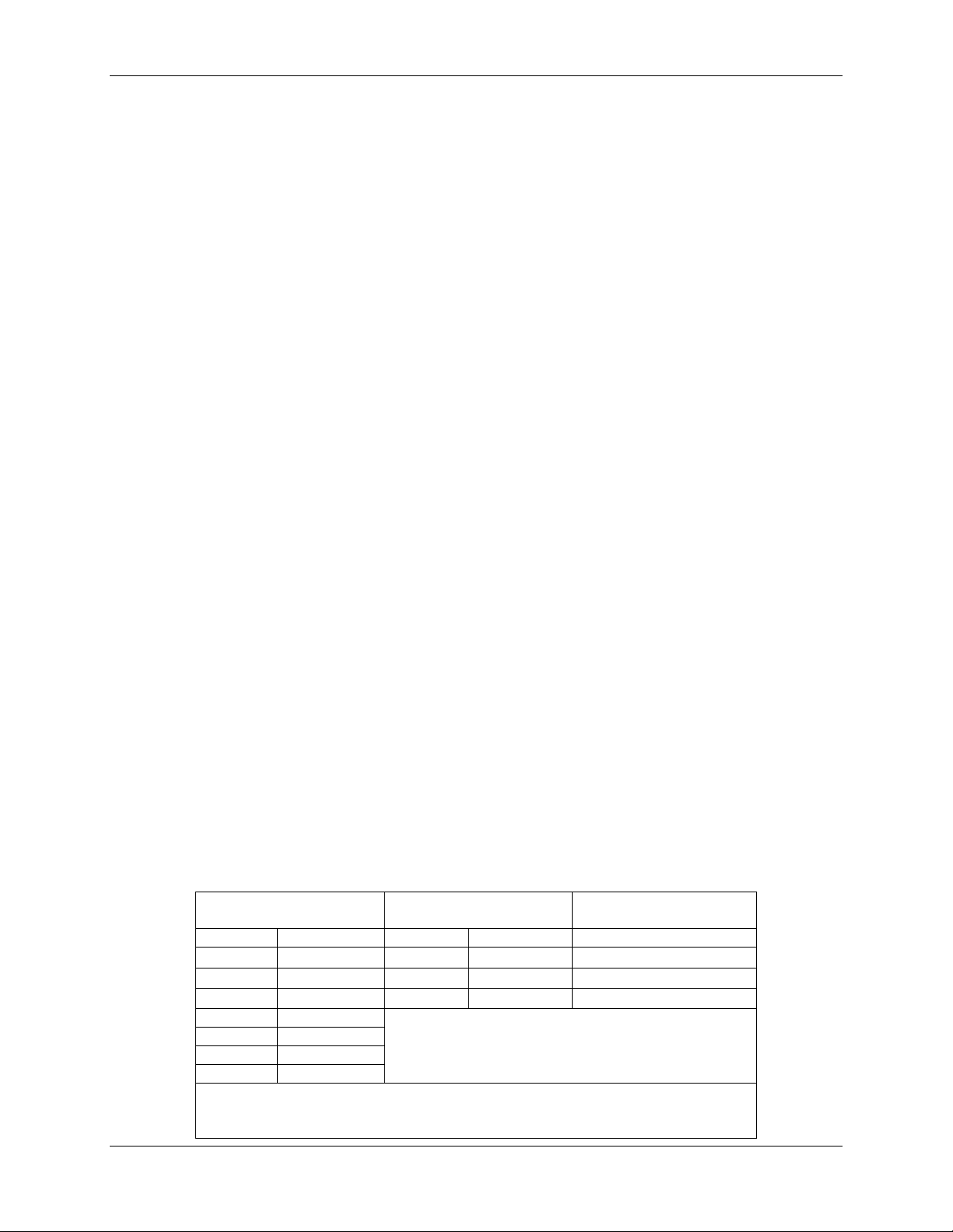
Data Sheet 71M6545/H PDS_6545_009
Command
Phase Selecto r
Associated TMUXRn
Control Field
000
Invalid
00
Invalid
---
001
Command 1
01
TMUXR2[2:0]
010
Command 2
10
011
Reserved
11
TMUXR6[2:0]
100
Reserved
101
Invalid
110
Reserved
111
Reserved
Notes:
operation. These are RCMD[4:2] = 001 and 010. Codes 000 and 101
communicati on with the 71M6545/H, supplying curr ent sampl es and auxiliary information such as sensor
temperature via a serial data stream.
Up to three 71M6xx3 Isolated Sensors ca n be su pp ort ed by t he 71M6545/H. When a remot e se n sor
interface is enabled, the two analog current inputs become re-configur ed and a digital remote sensor
interfac e. For exam ple, when control bit RMT2_E = 1 , the IADC2-IADC3 analog pins are re-configured as
the digital interface pins to the remote sensor.
Each 71M6xx3 Isolated Sensor consists of the f ollowing building blocks:
• Power supply that derives power from pulses received from the 71M6545/H
• Bi-directional di gital communications interf ac e
• Shunt signal pre-amplifier
• 22-bit 2nd Order Sigma-Delta ADC Converter with precision bandgap reference (choppi ng am plifier)
• Temperature sensor (for digitally compensati ng V REF)
• Fuse system contai ning par t-specific information
During an ordinar y multiplexer cycle, t he 71M6545/H internally determines which other channels are
enabled with MUX_DIV[3:0] (I/O RAM 0x2100[7:4]). At the same time, it decimates the modulator output
from the 71M6xx3 Isolated Sensors. Eac h r esul t is written to CE RAM during one of its CE access time
slots.
2.2.8.2 Communi cat io n b etween 71M6545/H and 71M6xx3 Isolated Sensor
The ADC of the 71M6xx3 derives its timing from the power pulses generated by the 71M6545/H and as a
result, operates its ADC slaved to the frequency of the power pulses. The generation of power pulses, as
well as the communication protocol between the 71M6545/H and 71M6xx3 Isolated Sensor, is automatic and
transparent to the user. Details are not covered in this data sheet.
2.2.8.3 Control of the 71M6xx3 Isolated Sensor
The 71M6545/H can read or write certain types of information from each 71M6xx3 remote sensor.
The data to be read is selected by a combination of the RCMD[4:0] and TMUXRn[2:0]. To perform a read
transaction from one of the 71M6xx3 devices, the MPU first writes the TMUXRn[2:0] field (where n = 2, 4, 6,
located at I/O RAM 0x270A[2:0], 0x270A[6:4] and 0x2709[2:0], respectively). Next, the MPU writes
RCMD[4:0] (SFR 0xFC[4:0]) with the desired command and phase selection. When the RCMD[4:2] bits
have cleared to zero, the transaction has been completed and the requested data is availabl e in
RMT_RD[15:0] (I/O RAM 0x260 2[ 7:0] is the MS B and 0x2603[7:0] is the LSB). The read parity error bit,
PERR_RD (SFR 0xFC[6]) is also updated during the transaction. If the MPU writes to RCMD[4:0] before a
previously init iated read transaction is completed, the command is ignored. Therefore, the MPU must wait
for RCMD[4:2]=0 befor e pr oc eeding to issue the next remote sensor read command.
The RCMD[4:0] field is divided into two sub-fields, COMMAND=RCMD[4:2] and PHASE=RCMD[1:0], as
shown in Table 4.
22 © 2008–2011 TERIDIA N Semiconduc tor Corporation v1.0
Table 4. RCMD[4:0] Bits
RCMD[4:2]
RCMD[1:0]
IADC2-IADC3
IADC4-IADC5
IADC6-IADC7
TMUXR4[2:0]
1. Only t wo codes of RCMD[4:2] (SFR 0xFC[4:2]) are relevant for norm al
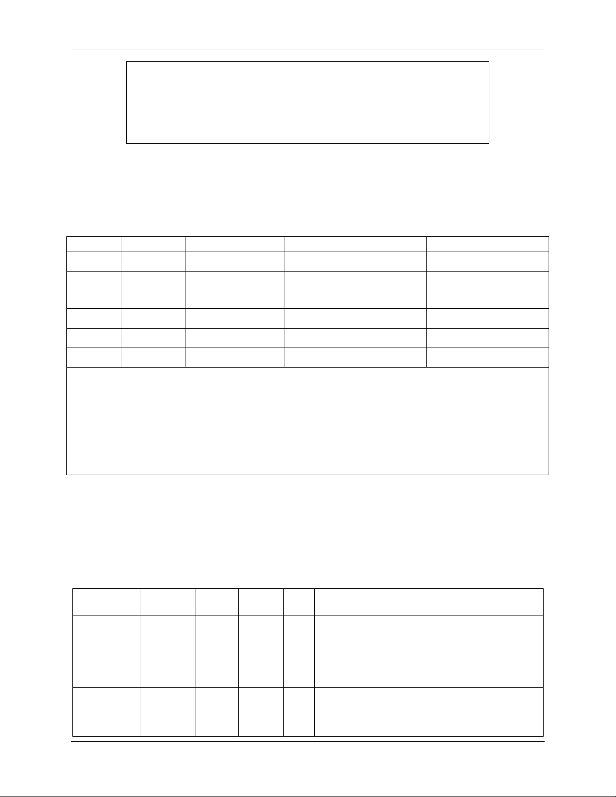
PDS_6545_009 Data Sheet 71M6545/H
are invalid and will be ignor ed if used. The remaining codes are
meter design.
VERSION[7:0]
Notes:
When the MPU wr ites a no n-zero value to RCMD,
reserved and must not be used.
2. For the RCMD[1:0] control field, codes 01, 10 and 11 are v alid and 00
is invalid and must not be used.
3. The specifi c phase (A, B or C) associated with each TMUXRn[2:0]
field , is determined by how the IADCn input pins are connected i n the
Table 5 shows the allowable combinations of values in RCMD[4:2] and TMUXRn[2:0], and the
corresponding data type and format sent back by the 71M6xx3 remote sensor and how the data is stored
in RMT_RD[15:8] and RMT_RD[7:0]. The MPU selects which of the three phases is read by assert ing the
proper code in the RCMD[1:0] field, as shown in Table 4.
Table 5: Remote Interface Read Commands
RCMD[4:2] TMUXRn[2:0] Read Operation RMT_RD [15:8] RMT_RD [7:0]
001 00X
001 11X
010 00X
010 01X
010 10X
TRIMT[7:0]
(trim fuse for all 71M6xx3)
TRIMBGB[7:0] and
TRIMBGD[7:0]
(additional trim fuses for
71M6113 and 71M6203 only)
STEMP[10:0]
(sensed 71M6xx3 temperature)
VSENSE[7:0]
(sensed 71M6xx3 supply voltage)
(chip version)
TRIMT[7]=RMT_RD[8] TRIMT[6:0]=RMT_RD[7:1]
TRIMBGB[7:0] TRIMBGD[7:0]
STEMP[10:8]=RMT_RD[10:8]
(RMT_RD[15:11] are si gn ext ended)
All zeros VSENSE[7:0]
VERSION[7:0]
All zeros
STEMP[7:0]
1. TRIMT[7:0] is t he VREF t rim value for all 71M6xx3 devices. No te th at the TRIMT[7:0] 8-bi t valu e i s formed
by RMT_RD[8] and RMT_RD[7:1]. See the 71M6xxx Data Sheet for the equations related to
and the corresponding temperature coefficient .
2. TRIMBGB[7:0] and TRIMBGD[7:0] are trim values used for characterizing the 71M6113 (0.5%) and 71M6203
(0.1%) over temperature. See the 71M6xxx Data sheet for the equations related to
TRIMBGD[7:0] and the corresponding temperature coefficients.
3. See 2.5.6
4. See 2.5.8
71M6xx3 Temperature Sensor on page 54.
71M6xx3 VCC Monitor on page 55.
With hardware and trim-related information on each connected 71M6xx3 Isolated Sensor available to the
71M6545/H, the MPU can implement temperature compensation of the energy measurement based on the
individual t em per ature characteristics of the 71M6xx3 Isolated Sensors. See 4.5 Metrology Temperature
Compensation for detail s .
Table 6 shows all I/O RAM registers used f or c ontrol of the external 71M6xx3 Isolated Sensors. See the
71M6xx3 Data Sheet for additional details.
Table 6: I/O RAM Control Bits for Isolated Sensor
RST
Default
Name Address
RCMD[4:0]
PERR_RD
PERR_WR
SFR
FC[4:0]
SFR FC[6]
SFR FC[5]
WAKE
Default
R/W Description
0 0 R/W
0 0 R/W
TRIMT[7:0]
TRIMBGB[7:0] and
the 71M6545/H issues a command to the corresponding isol ated sensor selected with
RCMD[1:0]. When the command is complete, the
71M6545/H clears RCMD[4:2]. The command
code itself is in RCMD[4:2].
The 71M6545/H sets these bits to indi c ate t hat a
parity error on the i sol ated sensor has been detected. Once s et, the bits are remembered until
they are cleared by the MPU.
v1.0 © 2008–2011 Teridian Semiconductor Corporation 23

Data Sheet 71M6545/H PDS_6545_009
Default
Default
The CHOP settings for the isolated sensors.
11 – Same as 00
TMUXR2[2:0]
270A[2:0]
000
000
R/W
The TMUX bits for control of the isolated sensor.
TMUXR4[2:0]
TMUXR6[2:0]
2709[2:0]
000
000
R/W
The TMUX bits for control of the isolated sensor.
RMT_RD[15:8]
2602[7:0]
2603[7:0]
Controls how the 71M6545/H drives the 71M6xx3
Enables the isolated remote sensor interface and
Enables the isolated remote sensor interface and
pair digital remote interface.
Refer to Table 61 start ing on page 88 for more complete details about these I/ O RAM l oc ations.
Name Address
CHOPR[1:0]
RMT_RD[7:0]
RFLY_DIS 210C[3]
RMT2_E
RMT4_E
RMT6_E
2709[7:6] 00 00 R/W
270A[6:4] 000 000 R/W The TM UX bits for control of the isolated sensor.
2709[3] 0 0 R/W
2709[4] 0 0 R/W
2709[5] 0 0 R/W
RST
0 0 R The read buffer for 71M6xx3 read operations.
0 0 R/W
WAKE
R/W Description
00 – Auto chop. Change every multiplexer frame.
01 – Positive
10 – Negative
power pulse. When set, the power pulse i s driven
high and low. When cleared, it is driven high
followed by an open circ uit flyback interval.
re-configures pins IADC2-IADC3 as a balanced
pair digital remote interface.
Enables the isolated remote sensor interface and
re-configures pins IADC4-IADC5 as a balanced
pair digital remote interface.
re-configures pins IADC6-IADC7 as a balanced
24 © 2008–2011 TERIDIA N Semiconduc tor Corporation v1.0

PDS_6545_009 Data Sheet 71M6545/H
2.3 Digital Computation Engine (CE)
The CE , a dedicated 32-bit si gnal process or, performs the precision computations necessar y to accurately
measure energy. The CE cal c ulations and processes include:
• Multiplicati on of each current sample with its associat ed voltage sample to obtain the energy per
sample (when multi plied by the constant sample time).
• Frequency-insensit ive delay cancellati on on all c hannels (t o c om pensate for the delay between
samples caused by the multiplexing scheme).
• 90° phase shifter (for VAR calc ulations).
• Pulse generation.
• Monitoring of the input signal frequency (for frequency and phase i nformation).
• Monitoring of the input signal amplitude (for sag detec tion).
• Scaling of the processed sam ples based on calibration coeffic ients.
• Scaling of sampl es based on temperature compensation i nformation.
2.3.1 CE Program Memor y
The CE program resides in flash memory. Common access to flash memory by the CE and MPU is
controlled by a memory share circuit. Each CE instruction word is two bytes long. Allocated flash space
for the CE program cannot exceed 4096 16-bi t words (8 KB). The CE program counter begins a pass
through the CE code each time m ultiplexer state 0 begins. The code pass ends when a HALT instruc tion
is executed. For proper oper ation, the code pass must be completed befor e the multiplexer cycle ends.
The CE program must begin on a 1 KB boundary of the flash addre ss. The I/O RAM con trol field
CE_LCTN[5:0] (I/O RAM 0x2109[5:0]) defi nes which 1 KB boundary c ontains the CE code. Thus, the first
CE instruction is l oc ated at 1024*CE_LCTN[5:0].
2.3.2 CE Data Memory
The CE and MPU share data memory (RAM). Common access to XRAM by the CE and MPU is controlled
by a memory share circuit. The CE can acc ess up to 3 KB of the 5 KB data RAM (XRAM), i.e. from RAM
address 0x0000 to 0x0C00.
The XRAM can be accessed by the FIR filt er bloc k, the RTM circuit, the CE, and the MPU. Assigned time
slots are reserved for FIR and MPU, respectively, to prevent bus contention for XRAM data access by the CE.
The MPU reads and writ es the XRAM share d between the CE and MPU as the primary means of data
communicati on between the two processors.
The CE is aided by suppor t har dware to facilitate implement ation of equations, pulse counters, and
accumulators. This hardware is controlled thr ough I/ O RAM field EQU[2:0] (equation assist, I/O RAM
0x2106[7:5]), bit DIO_PV (I/O RAM 0x2457[6]), bit DIO_PW (pulse count assist, I/O RAM 0x2457[7]), and
SUM_SAMPS[12:0] (accumulation assist, I/O RAM 0x2107[4:0] and 0x2108[7:0]).
The integration time for each energy output, when using standard CE code, is SUM_SAMPS[12:0] /2184.53
(with MUX_DIV[3:0] = 7, I/O RAM 0x2100[7:4] ). CE hardware issues the XFER_BUSY interrupt when the
accumulation is complete.
2.3.3 CE Communication with the MPU
The CE outputs six signals to the MPU: CE_BUSY, XFER_BUSY, XPULSE, YPULSE, WPULSE and
VPULSE. These are connected to the MPU interrupt servic e. CE_B USY indicates that the CE is actively
processing data. CE_BUSY occurs once every multiplexer frame. XFER_BUSY indicates that the CE is
updating to the output region of the CE RAM, which occurs whenever an accumulation cycle has been
completed. Both, CE_BUSY and XFER_BUSY are cleared when the CE executes a HALT instruction.
XPULSE and YPULSE can be confi gur ed to int er r upt the MPU and indicate sag failures, zero crossings of
the mains voltage, or other signif ic ant events. Additionally, these signals can be connected directly to DIO
pins to provide direct outputs from the CE. Interrupts associated with these signal s al ways occur on t he
leading edge.
v1.0 © 2008–2011 Teridian Semiconductor Corporation 25
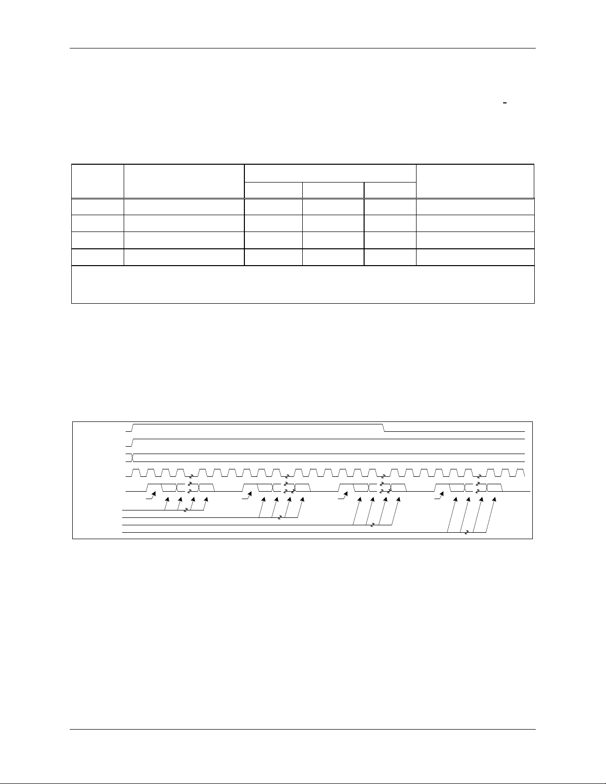
Data Sheet 71M6545/H PDS_6545_009
Element 0
Element 1
Element 2
2-elem ent, 3-W, 3φ Delta
Note:
CKTEST
RTM
FLAG
RTM DATA0 (32 bits)
LSB
SIGN
LSB
SIGN
RTM DATA1 (32 bits)
LSB
LSB
SIGN
SIGN
RTM DATA2 (32 bits)
RTM DATA3 (32 bits)
0 1
30 31
0 1
30 31
0 1
30 31
0 1
30 31
FLAG
FLAG
FLAG
MUX_STATE
S
MUX_SYNC
CK32
2.3.4 Meter Equations
The 71M6545/H provides hardware assistance to the CE i n order t o support v ari ous meter equations.
This assistance is controlled through I/O RAM field EQU[2:0] (equation assist, I/O RAM 0x2106[7:5])
Compute Engine (CE) firmware for industrial configurations can implement the equations li sted in
EQU[2:0] specifies the equa t ion to be used bas ed on th e meter configurati on and on t he numbe r o f phases
used for metering.
Table 7: Inputs Selected in Multiplexer Cycles
. The
Table 7.
EQU[2:0]*
2
3
4
5
Description
2-elem ent, 4-W, 3φ Delta
2-element, 4-W, 3φ Wye
3-element, 4-W, 3φ Wye
Wh and VARh formula
VA ∙ IA VB ∙ IB N/A IA VA IB VB
VA(IA-IB)/2 VC ∙IC N/A IA VA IB VB IC VC
VA(IA-IB)/2 VB(IC-IB)/2 N/A IA VA IB VB IC VC
VA ∙ IA VB ∙ IB VC ∙ IC IA VA IB VB IC VC (ID)
Recommended
Multiplexer Sequence
* Only EQU[2:0] = 5 is supported by the c ur r ently available CE code versions for the 71M6545/H.
Contact your local Teridian representativ e for CE codes that support equations 2, 3 and 4.
2.3.5 Real-Time Monit or (RTM)
The CE contains a Real-Time Monitor (RTM) , which can be programmed to monitor four selectable XRAM
locations at full sample rate. The data from the four monitored locations are serially output to the TMUXOUT
pin v ia the di gital output m ultiplexer at the beginning of each CE code pass. The RTM can be enabled and
disabled with RTM_E (I/O RAM 0x2106[1]). The RTM output clock is available on the TMUX2OUT pin.
Each RTM word is cloc k ed out i n 35 cycle s and contains a l eadin g flag bit. See Figure 8 for the RTM o utput
format. RTM is low when not in us e.
2.3.6 Pulse Generators
The 71M6545/H provides four pulse generators, VPULSE, WPULSE, XPULSE and YPULSE, as well as
hardware support for the VPULSE and WPULSE pulse generators. The XPULSE and YPULSE generators
are used by standard CE code to output CE status i ndic ators, for ex ample the status of the sag detecti on,
to DIO pins. All pulses can be configur ed to generate interrupts to the MPU.
The polarity of the pulses may be inverted with PLS_INV (I/O RAM 0x210C[0]). When this bit is set, the
pulses are active high, rather than the more usual active low. PLS_INV inverts all the pulse outputs.
The function of each pulse generator is determined by the CE code and the MPU code m ust c onfigure the
corresponding pulse output s i n agr eement with the CE code. For example, standard CE c ode pr oduc es a
mains zero-crossing pulse on XPULSE and a SA G pulse on YPULSE.
26 © 2008–2011 Teridian Semiconductor Corpor ation v1.0
Figure 8: RTM Timing

PDS_6545_009 Data Sheet 71M6545/H
A common use of the zero-crossing pul ses is to generate interrupts i n or der to drive real-time clock
software in places where the m ains frequency is sufficientl y accurate to do so and also to adjust for
crystal aging. A common use for the SAG pulse is to generate an interrupt that alerts the MPU when mains
power is about to fail, so that the MPU code can store accumulated energy and other data to EEPROM
before the V3P3SYS supply v oltage actually drops.
2.3.6.1 XPULSE and YPULSE
Pulses generated by the CE may be ex ported to the XPULSE and YPULSE pulse output pins. Pins DIO6
and DIO7 are used for these pulses, r espect ively. Generally, the XPULSE and YP ULS E o utputs can be
updated once on each pass of the CE code.
See 5.4 CE Interface Description on page 100 for details.
2.3.6.2 VPULSE and WPU LSE
Referring to Figure 9, during each CE code pass the hardware stores exported WPULSE and VPULSE sign
bits in an 8-bit FIFO and outputs them at a specified interval. This permits the CE code to calculate the
VPULSE and WPULSE outputs at the beginning of its code pass and to rely on hardware to spread them
over the multiplexer frame. As seen in Figure 9, the FIFO is reset at the beginning of each m ultiplexer
frame. As also seen in Figure 9, the I/O RAM register PLS_INTERVAL[7:0] (I/O RAM 0x210B[7:0]) controls
the delay to t he fir st pulse update and the interv al betwe en subsequent updates. The LSB of the
PLS_INTERVAL[7:0] register is equivalent to 4 CK_FIR cycles (CK_FIR is typically 4.9152MHz if PLL_FAST=1
and ADC_DIV=0, but other CK_FIR frequencies are possible; see the ADC_DIV definition in Table 61.) If
PLS_INTERVAL[7:0]=0, the FIFO is deactivated and the pulse outputs are updated immediat ely.
The MUX frame duration in units of CK_FIR clock cycles is given by:
If PLL_FAST=1:
MUX fram e durat ion in CK_FIR cycles = [1 + (FIR_LEN+1) * (ADC_DIV+1) * (MUX_DIV)] * [15 0 / (ADC_DIV+1)]
If PLL_FAST=0:
MUX fram e durat ion in CK_FIR cycles = [3 + 3*(FIR_LEN+1) * ( ADC_DIV+1) * (MUX_DIV)] * [48 / (ADC_DIV+1)]
PLS_INTERVAL[7:0] in units of CK_ FIR cl ock cycles i s calcu lated by:
PLS_INTERVAL[7:0] = floor ( Mux frame duration in CK_FIR cycles / CE pulse updates per Mux frame / 4 )
Since the FIFO resets at t he beginning of each multiplexer frame, the user must specify
PLS_INTERVAL[7:0] so that all of the possible pulse updates occurring in one CE execution are output
the multiplexer frame completes. For instance, the 71M6545/H CE code outputs six updates per
before
multiplexer interval, and if the multiplexer interval is 1950 CK_FIR clock c ycles long, the ideal value for
the interv al is 1950/6/4 = 81.25. However, if PLS_INTERVAL[7:0] = 82, the sixth output occurs too late and
would be lost. In this case, t he pr oper v alue for PLS_INTERVAL[7:0] is 81 (i.e., round down the result).
Since one LSB of PLS_INTERVAL[7:0] is equal to 4 CK_ FI R clock cycles, the pulse ti me interv al TI in u nits of
CK_FIR clock cycle s is:
TI = 4*PLS_INTERVAL[7:0]
If the FIFO is enab led (i.e ., PLS_INTERVAL[7:0] ≠ 0), hardware also provides a maximum pulse width feature
in control register PLS_MAXWIDTH[7:0] (I/O RAM 0x210A) . By default, WPULSE and VPULSE are negative
pulses ( i. e . , low level pulses, designed to sink c ur r ent through an LE D) . PLS_MAXWIDTH[7:0] determines the
maximum negative pulse wid th T
in uni t s of CK_FIR cl oc k cy c le s ba se d on th e p ul se i nt e rv al TI
MAX
according to the formula:
= (2 * PLS_MAXWIDTH[7:0] + 1) * TI
T
MAX
If PLS_MAXWIDTH = 255 or PLS_INTERVAL=0, no pulse widt h c hec k ing is performed, and the pulses
default to 50% duty cycl e.
The polarity of the pulses may be inverted with the control bit PLS_INV (I/O RAM 0x210C[0]). When
PLS_INV is set, the pulses are active high. The default value for PLS_INV is zero, which selects active low
pulses.
v1.0 © 2008–2011 Teridian Semiconductor Corporation 27
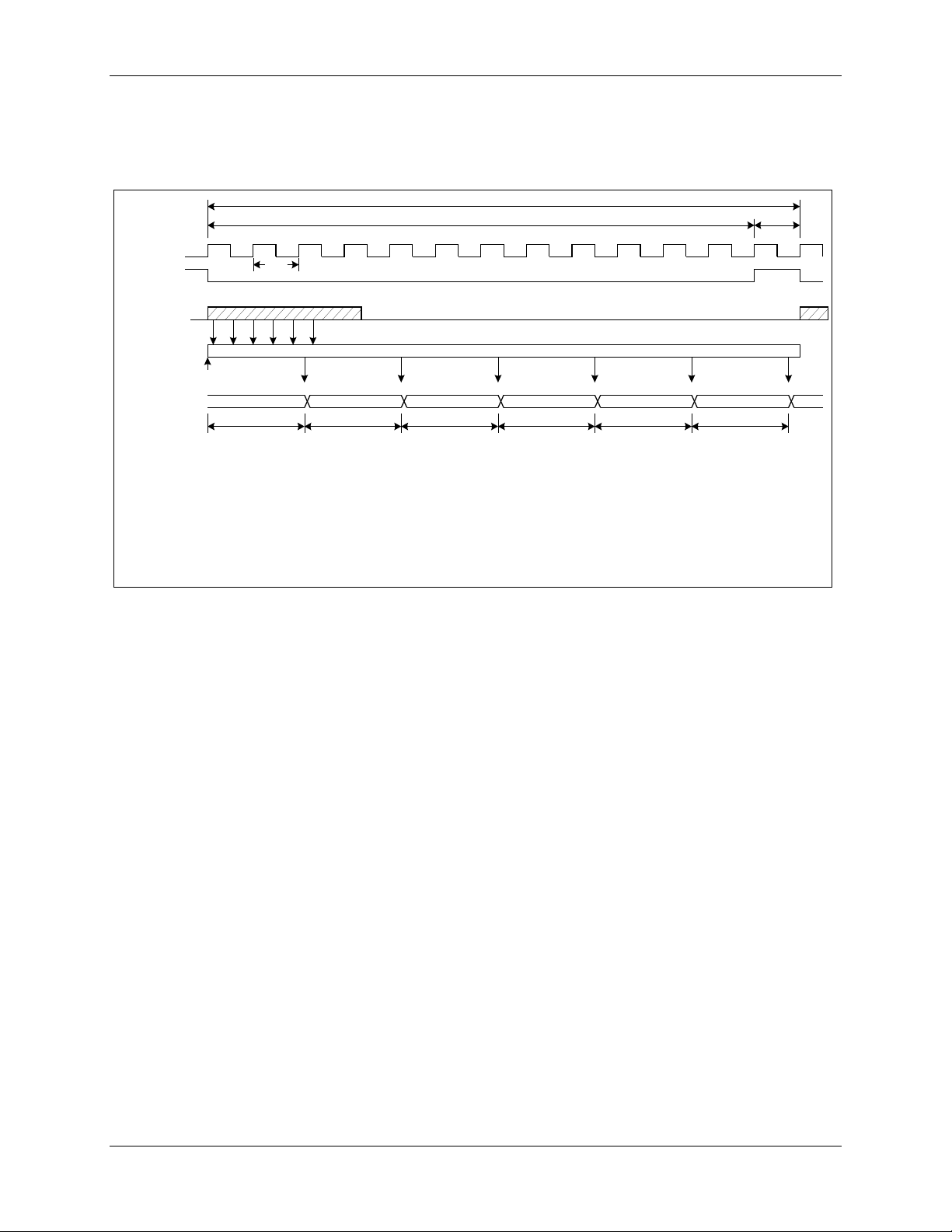
Data Sheet 71M6545/H PDS_6545_009
CK32
MUX_DIV Conversions (MUX_DIV=4 is shown) Settle
ADC MUX Frame
MUX_SYNC
150
WPULSE
S0S
1S2
S
3
S4S
5
CE CODE
RST
W_FIFO
S
0
S
1
S
2
S
3
S
4
S
5
S
0
S
1
S
2
S
3
S
4
S
5
4*PLS_INTERVAL
2. If WPULSE is low longer than (2*PLS_MAXWIDTH+1) updates, WPULSE will be raised until the next
low-going pulse begins.
3. Only the WPULSE circuit is shown. The VARPULSE circuit behaves identically.
4. All dimensions are in CK_FIR cycles (4.92MHz).
5. If PLS_INTERVAL=0, FIFO does not perform delay.
4*PLS_INTERVAL 4*PLS_INTERVAL
4*PLS_INTERVAL
4*PLS_INTERVAL 4*PLS_INTERVAL
1. This example shows how the FIFO distributes 6 pulse generator updates over one MUX frame.
The WPULSE and VPULSE pulse generator out puts are available on pins DIO0/WPULSE and
DIO1/VPULSE, respectively (pins 45 and 44). The pulses can also be output on OPT_TX pin 53 (see
OPT_TXE[1:0], I/O RAM 0x2456[3:2] for details).
Figure 9. P uls e Ge ne r a t or FI FO Timing
2.3.7 CE Functional Overview
The ADC processes one sample per c hannel per multiplexer cycle. Figure 10 shows the timing of the
samples taken during one multiplexer cycle with MUX_DIV[3:0] = 7 (I/O RAM 0x2100[7:4]).
The number of samp les pro ces s ed dur ing one ac cu mu lation cycle is controlled by the I/O RAM register
SUM_SAMPS[12:0] (0x2107[4:0] and 0x2108[7:0]). The inte gra tion time for each energy out pu t is:
SUM_SAMPS[12:0] / 2184.53, where 2184.53 is the sample rate in Hz
For ex ample, SUM_SAMPS[12:0] = 2184 establishes 2184 multiplexer cycles per accumulation cycle or
2184/2184.53 = 0. 9998 seconds. After an accumulation cycle is com pleted, the XFER_BUSY interrupt
signals to the MPU that accum ulated data are available. The slight difference between the nominal
length of the accum ulation interval (1000 ms) and the actual length of 999.8 ms (0.025%) is accounted for
in the CE code and is of no practical consequence.
28 © 2008–2011 Teridian Semiconductor Corpor ation v1.0
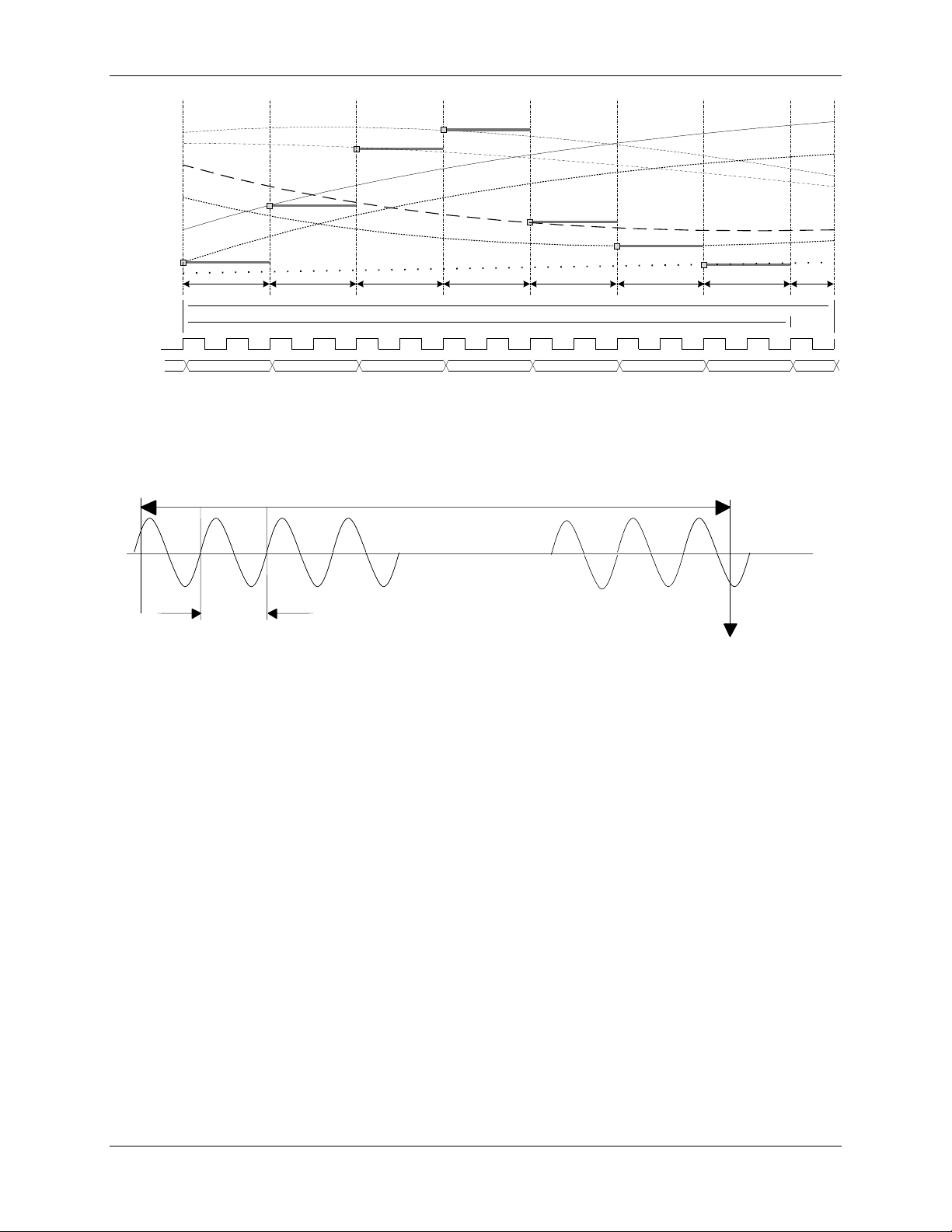
PDS_6545_009 Data Sheet 71M6545/H
MUX
STATE
CK32
(32768 Hz)
0 31 2
MUX_DIV = 7 Conversions
Settle
Multiplexer Frame (15 x 30.518 µs = 457.8 µs)
SS
IA
VA
IB
30.5 µs
61.04 µs
VB
61.04 µs
IC
VC
4 5 6
61.04 µs 61.04 µs
ID
XFER_BUSY
Interrupt to MPU
20ms
833ms
Figure 10: Samples from Multiplexer Cycle (Frame)
The end of each multiplexer cycle is signaled to the MPU by the CE_BUSY interrupt. At the end of each
multiplexer cycle, status information, such as sag data and the digitized input signal, is available to the MPU.
Figure 11 shows the accum ulation interval resul ting from SUM_SAMPS[12:0] = 1819 (I/O RAM
0x2107[4:0] and 0x2108[7:0]), consisting of 1819 samples of 457.8 µ s each, followed by the XFER_BUSY
interrupt. The sampling in this example is applied to a 50 Hz signal. There i s no corr elation between the
line signal frequency and the choice of SUM_SAMPS[12:0]. Furthermore, sampling does not have to start
when the line voltage cross es the zero line, and the length of the accumul ation interval need n ot be an
integer multi ple of the signal cycles.
v1.0 © 2008–2011 Teridian Semiconductor Corporation 29
Figure 11: Accumulation Interval

Data Sheet 71M6545/H PDS_6545_009
001
2.4576 MHz
2.4 80515 MPU Core
2.4.1 MPU Setup Code
For the proper operation of the 71M6545/H, it is necessary to have a small MPU program in flash
memory. In a typical application, the external host processor performs all post-pr oc essing and monitors
and controls the 71M6545/H over its SPI slave interface. T he following is a brief description of the tasks
performed by the requi r ed setup c ode. The setup code correctly configures the 71M6545/H to act as an
SPI Slave to a host processor, providing powerful AFE and 32-bit Metrology Processor functionali ty.
• The main objective of the setup code is to keep the MPU code execution confined to a small area
of Flash memory.
• Most of the Flash memory space is empty, except for the small setup progr am and the CE code.
• When ac power failure occ ur s, the MP U sets the SLEEP bit (I/O RAM 0x28B2[7]) bit) to force the
device to SLP mode (see 3.2 SLP Mode (Sleep Mode) on page 67).
• SFR (Special Function Registers) access is needed for configuri ng and c ontrolling the DIO0-
DIO14 pins. The SFRs of th e MPU cannot be ac c essed directly over the SPI Slave interface. If
the host requires contr ol of DIO0-DIO14, a small am ount of code i n the MP U provides the needed
SFR access.
• Triggering t he WDT reset.
• Controlling the 71M6xx3 Remote Sensor Interfaces, if used (temper ature data for CE).
• To speed up the start-up process and to off load the host processor, the small MP U program c an
implement the following optional steps at start-up:
- Copy CE data from flash to XRAM (default settings).
- Initialize the interrupt vector table.
- Initializ e the pointer to the CE code location.
- Initializ e the envir onm ental settings for the CE code (multiplex er and filter settings, etc.)
- Start the ADC and CE.
• It is also recommended t hat t he small MPU program maintains a counter that is incremented with
each XFER_BUSY interr upt. By reading this counter, the external host processor can determine if
any accumulat ed metr ology data were missed and if the 71M6545/H code is executing as
expected.
Sample MPU code that performs these simple tasks is available from Teridian.
During normal oper ation, the host processor needs to t ri gger the watchdog reset periodically in order to
avoid watchdog resets, if this is not done by the MPU program inside the 71M6545/H.
The remainder of this section provides detailed information concern in g the MPU, and may be
ignored if the application does not require the use of the MPU beyond the simple setup code tasks
described.
2.4.2 80515 MPU Overview
The 71M6545/H includes an 80515 MPU (8-bit, 8051-compatible) that processes most instructions in one
clock cycle. Using a 4.9 MHz clock resu lts in a processing throughput of 4.9 MIPS. The 80515 architecture
eliminates redundant bus states and implements parallel execution of fetch and execution phases. Normally, a
machine cycle is aligned with a memory fetch, therefore, most of the 1-byte instructions are performed in a
single machine cycle (MPU clock cycle). This leads to an 8x average performance improvement (in terms of
MIPS) over the Intel
Table 8 shows the CKMPU frequency as a func tion of the MCK clock (19.6608 MHz) divided by the MPU
clock divider MPU_DIV[2:0] (I/O RAM 0x2200[2:0]). Actual processor clocking speed can be adjusted to
the total processing demand of the application (meteri ng cal c ulations, AMR management, memory
management and I/O management) using MPU_DIV[2:0], as shown in Table 8.
8051 device running at the same clock frequency.
Table 8: CKMPU Clock Frequencies
MPU_DIV [2:0]
000 4.9152 MHz
CKMPU Frequency
30 © 2008–2011 Teridian Semiconductor Corpor ation v1.0
 Loading...