

TERIDIAN Semiconductor 71M6531DF, 71M6532DF Technical data
71M6531D/F, 71M6532D/F
Energy Meter IC
MPU
TIMERS
IAP*
VA
IBP*
XIN
XOUT
VREF
RX/DIO1
TX/DIO2
V1
TX
RX
COM0..3
V3.3A
V3.3
SYS
VBAT
V2.5
VBIAS
GNDA GNDD
SEG/DIO
ICE I/F
LOAD
88. 88.8888
I2C or µWire
EEPROM
POWER
FAULT
AMR
TEST PULSES
COMPARATOR
SENSE
DRIVE/MOD
SERIAL PORTS
OSC/PLL
ADC
LCD & DIO
COMPUTE
ENGINE
FLASH
MEMORY
RAM
VOLTAGE REF
REGULATOR
POWER SUPPLY
TERIDIAN
71M6531
71M6532
TEMP
SENSOR
32 kHz
A
NEUTRAL
CT/SHUNT
02/18/2009
VB
B
LOAD
IR
PWR MODE
CONTROL
WAKE-UP
BATTERY
ICE_E GNDD
V3P3D
IAN*
IBN*
CT
SPI HOST
SPI
LCD SEG
RTC
*
Differential pins only on 6532D/F
Simplifying System Integration
TM
DATA SHEET
June 2010
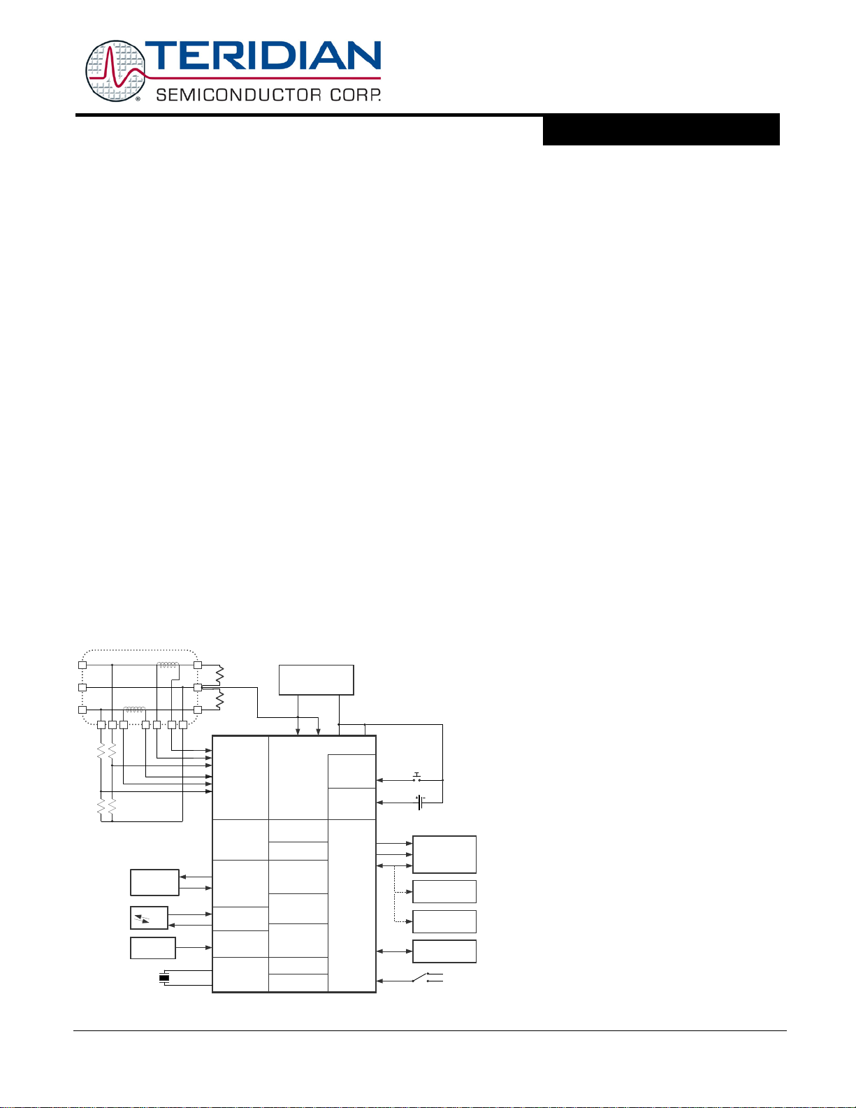
GENERAL DESCRIPTION
The Teridian 71M6531D/F and 71M6532D/F are highly
integrated SOCs with an MPU core, RTC, FLASH and LCD
driver. Teridian’s patented Single Converter Technology®
with a 22-bit delta-sigma ADC, four ana log inputs, digital
temperature compe nsation, precisio n voltage r eference, battery
voltage monitor and 32-bit computation engine (CE) supports
a wide range of residential metering applications with very few
low-cost external components.
A 32-kHz crystal time base for the entire system and internal
battery backup support for RAM and RTC further reduce system
cost. The IC suppor ts 2-wire, and 3-wire single-phase and
dual-phase residential metering along with t am per-detection
mechanisms. The 71M6531D/F offers single-ended inputs for
two current channels and two single-ended voltage inputs.
The 71M6532D/F has two differential current inputs and three
single-ended voltage inputs.
2
Maximum design flexibility is provided by multiple UARTs, I
μWire, up to 21 DIO pins and in-system programmable FLASH
memory, which can be updated with data or application code
in operation.
A complete array of ICE and development t ool s, programming
libraries and reference designs enable rapid development and
certification of TOU, AMR and Prepay meters that comply with
worldwide electricity metering standards.
C,
FEATURES
• Wh accuracy < 0.1% over 2000:1 current
range
• Exceeds IEC62053/ANSI C12.20 standards
• Four sensor inputs
• Low-jitter Wh and VARh plus two additional
pulse test outputs (4 total, 10 kHz maximum)
with pulse count
• Four-quadrant metering
• Tamper detection (Neutral current with CT,
Rogowski or shunt, magnetic tamper input)
• Line frequency count for RTC
• Digital temperature compensation
• Sag detection for phase A and B
• Independent 32-bit compute engine
• 46-64 Hz line frequency range with same
calibration. Phase compensation (± 7°)
• Three battery modes with wake-up on timer
or push-button:
Brownout mode (52 µA typ.)
LCD mode (21 µA typ., DAC active)
Sleep mode (0.7 µA typ.)
• Energy display during mains power failure
• 39 mW typical consumption @ 3.3 V, MPU
clock frequency 614 kHz
• 22-bit delta-sigma ADC with 3360 Hz or
2520 Hz sample rate
• 8-bit MPU (80515),1 clock cycle per instruction,
10 MHz maximum, with integrated ICE for
debug
• RTC for TOU functions with clock-rate adjust
register
• Hardware watchdog timer, power fail monitor
• LCD driver with 4 common segment drivers:
Up to 156 (71M6531D/F) or 268 pixels
(71M6532D/F)
• Up to 22 (71M6531D/F) or 43 (71M6532D/F)
general-purpose I/O pins. Digital I/O pins
compatible with 5 V inputs
• 32 kHz time base
v1.3 © 2005-2010 TERIDIAN Semiconductor Corporation 1
• High-speed slave SPI interface t o data RAM
• Two UARTs for IR and AMR, IR driver with
modulation
• FLASH memory with security and in-system
program update:
128 KB (71M6531D/32D)
256 KB (71M6531F/32F)
• 4 KB MPU XRAM
• Industrial temperature range
• 68-pin QFN package for 71M6531D/F pin-
compatible with 71M6521, 100-pin LQFP
package for 71M6532D/F, lead free

Data Sheet 71M6531D/F-71M6532D/F FDS 6531/6532 005
Table of Contents
1 Hardware Description ....................................................................................................................... 10
1.1 Hardware Overview ................................................................................................................... 10
1.2 Analog Front End (AFE) ............................................................................................................. 10
1.2.1 Signal Input Pins ............................................................................................................ 10
1.2.2 Input Multiplexer ............................................................................................................ 11
1.2.3 A/D Converter (ADC) ..................................................................................................... 12
1.2.4 FIR Filter ........................................................................................................................ 12
1.2.5 Voltage References ....................................................................................................... 12
1.2.6 Temperature Sensor ...................................................................................................... 14
1.2.7 Battery Monitor............................................................................................................... 14
1.2.8 AFE Functional Description ........................................................................................... 14
1.2.9 Digital Computation Engine (CE) ................................................................................... 15
1.2.10 Meter Equations ............................................................................................................. 16
1.2.11 Real-Time Monitor ......................................................................................................... 16
1.2.12 Pulse Generators ........................................................................................................... 16
1.2.13 Data RAM (XRAM) ........................................................................................................ 17
1.2.14 Delay Compensation ..................................................................................................... 17
1.2.15 CE Functional Overview ................................................................................................ 17
1.3 80515 MPU Core ....................................................................................................................... 19
1.3.1 Memory Organization and Addressing .......................................................................... 19
1.3.2 Special Function Registers (SFRs) ............................................................................... 21
1.3.3 Generic 80515 Special Function Registers ................................................................... 22
1.3.4 Special Function Registers (SFRs) Specific t o the 71M6531D/F and 71M6532D/F ..... 24
1.3.5 Instruction Set ................................................................................................................ 26
1.3.6 UARTs ........................................................................................................................... 26
1.3.7 Timers and Counters ..................................................................................................... 28
1.3.8 WD Timer (Software Watchdog Timer) ......................................................................... 30
1.3.9 Interrupts ........................................................................................................................ 30
1.4 On-Chip Resources ................................................................................................................... 36
1.4.1 Oscillator ........................................................................................................................ 36
1.4.2 Internal Clocks ............................................................................................................... 36
1.4.3 Real-Time Clock (RTC) ................................................................................................. 37
1.4.4 Temperature Sensor ...................................................................................................... 38
1.4.5 Physical Memory............................................................................................................ 38
1.4.6 Optical Interface ............................................................................................................. 40
1.4.7 Digital I/O – 71M6531D/F .............................................................................................. 41
1.4.8 Digital I/O – 71M6532D/F .............................................................................................. 43
1.4.9 Digital IO – Common Characteristics for 71M6531D/F and 71M 6532D/F .................... 44
1.4.10 LCD Drivers – 71M6531D/F .......................................................................................... 45
1.4.11 LCD Drivers – 71M6532D/F .......................................................................................... 46
1.4.12 LCD Drivers – Common Characteristics for 71M6531D/ F and 71M6532D/F ............... 46
1.4.13 Battery Monitor............................................................................................................... 46
1.4.14 EEPROM Interface ........................................................................................................ 46
1.4.15 SPI Slave Port................................................................................................................ 49
1.4.16 Hardware Watchdog Timer ............................................................................................ 52
1.4.17 Test Ports (TMUXOUT pin) ........................................................................................... 53
2 © 2005-2010 TERIDIAN Semiconductor Corporation v1.3

FDS 6531/6532 005 Data Sheet 71M6531D/F-71M6532D/F
2 Functional Description ..................................................................................................................... 54
2.1 Theory of Operation ................................................................................................................... 54
2.2 System Timing Summary ........................................................................................................... 55
2.3 Battery Modes ............................................................................................................................ 56
2.3.1 BROWNOUT Mode ....................................................................................................... 57
2.3.2 LCD Mode ...................................................................................................................... 58
2.3.3 SLEEP Mode ................................................................................................................. 58
2.4 Fault and Reset Behavior .......................................................................................................... 60
2.4.1 Reset Mode .................................................................................................................... 60
2.4.2 Power Fault Circuit ........................................................................................................ 60
2.5 Wake-Up Behavior ..................................................................................................................... 61
2.5.1 Wake on PB ................................................................................................................... 61
2.5.2 Wake on Timer............................................................................................................... 61
2.6 Data Flow ................................................................................................................................... 61
2.7 CE/MPU Communication ........................................................................................................... 62
3 Application Information .................................................................................................................... 63
3.1 Connection of Sensors ............................................................................................................... 63
3.2 Connecting 5-V Devices ............................................................................................................ 63
3.3 Temperature Measurement ....................................................................................................... 64
3.4 Temperature Compensation ...................................................................................................... 64
3.4.1 Temperature Coefficients: ............................................................................................. 64
3.4.2 Temperature Compensation for VREF .......................................................................... 65
3.4.3 System Temperature Compensation ............................................................................. 65
3.4.4 Temperature Compensation for the RTC ...................................................................... 65
3.5 Connecting LCDs ....................................................................................................................... 66
3.6 Connecting I2C EEPROMs ........................................................................................................ 66
3.7 Connecting Three-Wire EEPROMs ........................................................................................... 67
3.8 UART0 (TX/RX) ......................................................................................................................... 67
3.9 Optical Interface (UART1) .......................................................................................................... 67
3.10 Connecting the V1 Pin ............................................................................................................... 68
3.11 Connecting the Reset Pin .......................................................................................................... 69
3.12 Connecting the Emulator Port Pins ............................................................................................ 69
3.13 Connecting a Battery ................................................................................................................. 69
3.14 Flash Programming .................................................................................................................... 70
3.15 MPU Firmware ........................................................................................................................... 70
3.16 Crystal Oscillator ........................................................................................................................ 70
3.17 Meter Calibration ........................................................................................................................ 71
4 Firmware Interface ............................................................................................................................ 72
4.1 I/O RAM and SFR Map – Functional Order ............................................................................... 72
4.2 I/O RAM Description – Alphabetical Order ................................................................................ 77
4.3 CE Interface Description ............................................................................................................ 88
4.3.1 CE Program ................................................................................................................... 88
4.3.2 CE Data Format ............................................................................................................. 88
4.3.3 Constants ....................................................................................................................... 88
4.3.4 Environment ................................................................................................................... 88
4.3.5 CE Calculations ............................................................................................................. 89
4.3.6 CE Status and Control ................................................................................................... 89
4.3.7 CE Transfer Variables ................................................................................................... 92
4.3.8 Pulse Generation ........................................................................................................... 93
4.3.9 CE Calibration Parameters ............................................................................................ 94
v1.3 © 2005-2010 TERIDIAN Semiconductor Corporation 3

Data Sheet 71M6531D/F-71M6532D/F FDS 6531/6532 005
4.3.10 Other CE Parameters .................................................................................................... 95
4.3.11 CE Flow Diagrams ......................................................................................................... 95
5 Electrical Specifications ................................................................................................................... 98
5.1 Absolute Maximum Ratings ....................................................................................................... 98
5.2 Recommended External Components ....................................................................................... 99
5.3 Recommended Operating Conditions ........................................................................................ 99
5.4 Performance Specifications ..................................................................................................... 100
5.4.1 Input Logic Levels ........................................................................................................ 100
5.4.2 Output Logic Levels ..................................................................................................... 100
5.4.3 Power-Fault Comparator ............................................................................................. 100
5.4.4 Battery Monitor............................................................................................................. 100
5.4.5 Supply Current ............................................................................................................. 101
5.4.6 V3P3D Switch .............................................................................................................. 101
5.4.7 2.5 V Voltage Regulator ............................................................................................... 101
5.4.8 Low-Power Voltage Regulator ..................................................................................... 101
5.4.9 Crystal Oscillator .......................................................................................................... 102
5.4.10 LCD DAC ..................................................................................................................... 102
5.4.11 LCD Drivers ................................................................................................................. 102
5.4.12 Optical Interface ........................................................................................................... 102
5.4.13 Temperature Sensor .................................................................................................... 103
5.4.14 VREF ........................................................................................................................... 103
5.4.15 ADC Converter, V3P3A Referenced ........................................................................... 104
5.5 Timing Specifications ............................................................................................................... 105
5.5.1 Flash Memory .............................................................................................................. 105
5.5.2 EEPROM Interface ...................................................................................................... 105
5.5.3 RESET ......................................................................................................................... 105
5.5.4 RTC .............................................................................................................................. 105
5.5.5 SPI Slave Port (MISSION Mode) ................................................................................. 106
5.6 Typical Performance Data ....................................................................................................... 107
5.6.1 Accuracy over Current ................................................................................................. 107
5.6.2 Accuracy over Temperature ........................................................................................ 107
5.7 71M6531D/F Package ............................................................................................................. 108
5.7.1 Package Outline .......................................................................................................... 108
5.7.2 71M6531D/F Pinout (QFN-68) ..................................................................................... 109
5.7.3 Recommended PCB Land Pattern for the QFN-68 Package ...................................... 110
5.8 71M6532D/F Package ............................................................................................................. 111
5.8.1 71M6532D/F Pinout (LQFP-100) ................................................................................. 111
5.8.2 LQFP-100 Mechanical Drawing ................................................................................... 112
5.9 Pin Descriptions ....................................................................................................................... 113
5.9.1 Power and Ground Pins ............................................................................................... 113
5.9.2 Analog Pins .................................................................................................................. 113
5.9.3 Digital Pins ................................................................................................................... 114
5.9.4 I/O Equivalent Circuits ................................................................................................. 115
6 Ordering Information ...................................................................................................................... 116
7 Related Information ........................................................................................................................ 116
8 Contact Information ........................................................................................................................ 116
Appendix A: Acronyms .......................................................................................................................... 117
Appendix B: Revision History ............................................................................................................... 118
4 © 2005-2010 TERIDIAN Semiconductor Corporation v1.3

FDS 6531/6532 005 Data Sheet 71M6531D/F-71M6532D/F
Figures
Figure 1: 71M6531D/F IC Functional Block Diagram ................................................................................... 8
Figure 2: 71M6532D/F IC Functional Block Diagram ................................................................................... 9
Figure 3: General Topology of a Chopped Ampli fier .................................................................................. 13
Figure 4: CROSS Signal with CHOP_E[1:0] = 00 ....................................................................................... 13
Figure 5: AFE Block Diagram (Shown for the 71M65 32D/F) ...................................................................... 14
Figure 6: Samples from Multiplexer Cyc le .................................................................................................. 18
Figure 7: Accumulation Interval .................................................................................................................. 18
Figure 8: Interrupt Structure ........................................................................................................................ 35
Figure 9: Optical Interface ........................................................................................................................... 41
Figure 10: Connecting an External Load to DIO Pins ................................................................................. 45
Figure 11: 3-Wire Interface. Write Command, HiZ =0 ................................................................................ 48
Figure 12: 3-Wire Interface. Write Command, HiZ =1 ................................................................................ 48
Figure 13: 3-Wire Interface. Read Command. ........................................................................................... 49
Figure 14: 3-Wire Interface. Write Command when CNT=0 ...................................................................... 49
Figure 15: 3-Wire Interface. Write Command when HiZ =1 and WFR=1 ................................................... 49
Figure 16: SPI Slave Port: Typical Read and Write operations .................................................................. 51
Figure 17: Functions defined by V1 ............................................................................................................ 52
Figure 18: Voltage, Current, Momentary and Ac cumulated Energy ........................................................... 54
Figure 19: Timing Relationship between ADC MUX, Compute Engine ...................................................... 55
Figure 20: RTM Output Format ................................................................................................................... 55
Figure 21: Operation Modes State Diagram ............................................................................................... 56
Figure 22: Transition from BROWNOUT t o M ISSION Mode when System Power Returns ...................... 59
Figure 23: Power-Up Timing with V3P3SYS and VBAT tied together ........................................................ 59
Figure 24: Power-Up Timing with VBAT only .............................................................................................. 60
Figure 25: Wake Up Timing ........................................................................................................................ 61
Figure 26: MPU/CE Data Flow .................................................................................................................... 62
Figure 27: MPU/CE Communication ........................................................................................................... 62
Figure 28: Resistive Voltage Divider ........................................................................................................... 63
Figure 29: CT with Single Ended (Left) and Diff erential Input (Right) Connection ..................................... 63
Figure 30: Resistive Shunt (Left) and Rogowski Sensor (Right) Connection ............................................. 63
Figure 31: Connecting LCDs ....................................................................................................................... 66
Figure 32: I2C EEPROM Connection .......................................................................................................... 66
Figure 33: Three-Wire EEPROM Connection ............................................................................................. 67
Figure 34: Connections for UART0 ............................................................................................................. 67
Figure 35: Connection for Optical Component s .......................................................................................... 68
Figure 36: Voltage Divider for V1 ................................................................................................................ 68
Figure 37: External Components for the RES E T Pin: Push-button (Left), Production Circuit (Right) ........ 69
Figure 38: External Components for the Em ulator Interface ...................................................................... 69
Figure 39: Connecting a Battery ................................................................................................................. 70
Figure 40: CE Data Flow: Multiplexer and ADC.......................................................................................... 96
Figure 41: CE Data Flow: Scaling, Gain Control, Intermediate Variables .................................................. 96
Figure 42: CE Data Flow: Squaring and Sum m ation Stages ...................................................................... 97
Figure 43: SPI Slave Port (MISSION Mode) Timing ................................................................................. 106
Figure 44: Wh Accuracy, 0.1 A to 200 A at 240 V/50 H z and Room Temperature .................................. 107
Figure 45: QFN-68 Package Outline, Top and Side View ........................................................................ 108
Figure 46: QFN-68 Package Outline, Bottom Vi ew .................................................................................. 108
Figure 47: Pinout for QFN-68 Package ..................................................................................................... 109
Figure 48: PCB Land Pattern for QFN 68 Package .................................................................................. 110
Figure 49: PCB Land Pattern for LQFP-100 Package .............................................................................. 111
Figure 50: LQFP-100 Package, Mechanical Dra wing ............................................................................... 112
Figure 51: I/O Equivalent Circuits ............................................................................................................. 115
v1.3 © 2005-2010 TERIDIAN Semiconductor Corporation 5

Data Sheet 71M6531D/F-71M6532D/F FDS 6531/6532 005
Tables
Table 1: Inputs Selected in Regular and Alternat e M ultiplexer Cycles ....................................................... 11
Table 2: ADC Resolution ............................................................................................................................. 12
Table 3: ADC RAM Locations ..................................................................................................................... 12
Table 4: XRAM Locations for ADC Results ................................................................................................ 15
Table 5: Meter Equations ............................................................................................................................ 16
Table 6: CKMPU Clock Frequencies .......................................................................................................... 19
Table 7: Memory Map ................................................................................................................................. 20
Table 8: Internal Data Memory Map ........................................................................................................... 21
Table 9: Special Function Register Map ..................................................................................................... 21
Table 10: Generic 80515 SFRs - Location and Reset Values .................................................................... 22
Table 11: PSW Bit Functions (SFR 0xD0) ..................................................................................................... 23
Table 12: Port Registers ............................................................................................................................. 24
Table 13: Stretch Memory Cycle Width ...................................................................................................... 24
Table 14: 71M6531D/F and 71M6532D/F Specific SF Rs ........................................................................... 24
Table 15: Baud Rate Generation ................................................................................................................ 26
Table 16: UART Modes ............................................................................................................................... 26
Table 17: The S0CON (UART0) Register (SFR 0x98) ................................................................................. 27
Table 18: The S1CON (UART1) register (SFR 0x9B) .................................................................................. 27
Table 19: PCON Register Bit Description (SFR 0x87) ................................................................................ 28
Table 20: Timers/Counters Mode Description ............................................................................................ 28
Table 21: Allowed Timer/Counter Mode Combinations .............................................................................. 29
Table 22: TMOD Register Bit Description (SFR 0x89) ................................................................................ 29
Table 23: The TCON Register Bit Functions (SF R 0x 88) ............................................................................ 29
Table 24: The IEN0 Bit Functions (SFR 0xA8) ............................................................................................ 30
Table 25: The IEN1 Bit Functions (SFR 0xB8) ............................................................................................ 31
Table 26: The IEN2 Bit Functions (SFR 0x9A) ............................................................................................ 31
Table 27: TCON Bit Functions (SFR 0x88) ................................................................................................. 31
Table 28: The T2CON Bit Functions (SFR 0xC8) ........................................................................................ 31
Table 29: The IRCON Bit Functions (SFR 0xC0) ........................................................................................ 31
Table 30: External MPU Interrupts .............................................................................................................. 32
Table 31: Interrupt Enable and Flag Bits .................................................................................................... 32
Table 32: Interrupt Priority Level Groups .................................................................................................... 33
Table 33: Interrupt Priority Levels ............................................................................................................... 33
Table 34: Interrupt Priority Registers (IP0 and IP1) .................................................................................... 34
Table 35: Interrupt Polling Sequence .......................................................................................................... 34
Table 36: Interrupt Vectors .......................................................................................................................... 34
Table 37: Clock System Summary .............................................................................................................. 36
Table 38: Bank Switching with FL_BANK[2:0] ............................................................................................ 40
Table 39: Data/Direction Registers and Internal Resources for DIO 1-15 (71M6531D/F) ......................... 42
Table 40: Data/Direction Registers and Internal Resources for DIO 17-29 (71M6531D/F) ....................... 42
Table 41: Data/Direction Registers and Internal Resources for DIO 43-46 (71M6531D/F) ....................... 42
Table 42: Data/Direction Registers and Internal Resources for DIO 1-15 (71M6532D/F) ......................... 43
Table 43: Data/Direction Registers and Internal Resources for DIO 16-30 (71M6532D/F) ....................... 43
Table 44: Data/Direction Registers and Internal Resources for DIO 40-51 (71M6532D/F) ....................... 44
Table 45: DIO_DIR Control Bit .................................................................................................................... 44
Table 46: Selectable Control using DIO_DIR Bits ......................................................................................... 44
Table 47: EECTRL Bits for 2-pin Interface ................................................................................................... 47
Table 48: EECTRL Bits for the 3-Wire Interface .......................................................................................... 48
Table 49: SPI Command Description .......................................................................................................... 50
Table 50: I/O RAM Registers Accessible via S P I ....................................................................................... 50
Table 51: TMUX[4:0] Selections ................................................................................................................. 53
Table 52: Available Circuit Functions .......................................................................................................... 57
6 © 2005-2010 TERIDIAN Semiconductor Corporation v1.3

FDS 6531/6532 005 Data Sheet 71M6531D/F-71M6532D/F
Table 53: I/O RAM Map in Functional Order ............................................................................................... 72
Table 54: I/O RAM Description - Alphabetical ............................................................................................ 77
Table 55: CE EQU[2:0] Equations and Element Input Mapping ................................................................. 89
Table 56: CESTATUS (CE RAM 0x80) Bit Definitions .................................................................................. 90
Table 57: CECONFIG Bit Definitions ........................................................................................................... 91
Table 58: Sag Threshold Control ................................................................................................................ 91
Table 59: Gain Adjust Control ..................................................................................................................... 91
Table 60: CE Transfer Variables ................................................................................................................. 92
Table 61: CE Energy Measurement Variables ............................................................................................ 92
Table 62: Useful CE Measurement Parameter s ......................................................................................... 93
Table 63: CE Pulse Generation Parameters ............................................................................................... 94
Table 64: CE Calibration Parameters ......................................................................................................... 94
Table 65: CE Parameters for Noise Suppressi on and Code Version ......................................................... 95
Table 66: Absolute Maximum Ratings ........................................................................................................ 98
Table 67: Recommended External Components ........................................................................................ 99
Table 68: Recommended Operating Condit ions ......................................................................................... 99
Table 69: Input Logic Levels ..................................................................................................................... 100
Table 70: Output Logic Levels .................................................................................................................. 100
Table 71: Power-Fault Comparator Performa nce Specifications ............................................................. 100
Table 72: Battery Monitor Performance Specifications (BME= 1) ............................................................. 100
Table 73: Supply Current Performance Specif i cations ............................................................................. 101
Table 74: V3P3D Switch Performance Specifi cat i ons .............................................................................. 101
Table 75: 2.5 V Voltage Regulator Performance Specifications ............................................................... 101
Table 76: Low-Power Voltage Regulator Performance Specifications ..................................................... 101
Table 77: Crystal Oscillator Performance Specifications .......................................................................... 102
Table 78: LCD DAC Performance Specifications ..................................................................................... 102
Table 79: LCD Driver Performance Specificat i ons ................................................................................... 102
Table 80: Optical Interface Performance Specifications ........................................................................... 102
Table 81: Temperature Sensor Performance Specifications .................................................................... 103
Table 82: VREF Performance Specifications ............................................................................................ 103
Table 83: ADC Converter Performance Specific ations ............................................................................. 104
Table 84: Flash Memory Timing Specifications ........................................................................................ 105
Table 85: EEPROM Interface Timing ........................................................................................................ 105
Table 86: RESET Timing .......................................................................................................................... 105
Table 87: SPI Slave Port (MISSION Mode) Timing .................................................................................. 106
Table 88: Recommended PCB Land Pattern Dimensions ........................................................................ 110
Table 89: Power and Ground Pins ............................................................................................................ 113
Table 90: Analog Pins ............................................................................................................................... 113
Table 91: Digital Pins ................................................................................................................................ 114
v1.3 © 2005-2010 TERIDIAN Semiconductor Corporation 7
Data Sheet 71M6531D/F-71M6532D/F FDS 6531/6532 005
∆Σ ADC
CONVERTER
VREF
ADC_E
MUX
XIN
XOUT
VREF
DIO1/OPT_RX
RESET
V1
UART2--OPTICAL
UART1
TX
RX
4
COM0...3
LCD DISPLAY
DRIVER
DIGITAL I/O
RTCLK (32KHz)
CE_E
RTM_E
POWER FAULT
LCD_E
LCD_CLK
LCD_MODE
DIO
GNDD V3P3A
V3P3D
VBAT
VOLT
REG
2.5V to logic
V2P5
SUM_CYCLES
PRE_SAMPS
EQU
TMUXOUT
FAULTZ
TMUX[4:0]
GNDA
VBIAS
OSC
(32KHz)
MCK
PLL
VREF
VREF_DIS
TEST
TEST
MODE
DIO_R
DIO_DIR
E_RXTX
OPT_TXE
RTC
VBIAS
ICE_E
VREF_CAL
RTM_0..3
CE_LCTN
PLS_MAXWIDTH
PLS_INTERVAL
PLS_INV
OPT_TXINV
OPT_TXMOD
OPT_FDC
OPT_RXINV
OPT_RXDIS
LCD_BLKMAP
LCD_SEG
LCD_Y
SLEEP
LCD_ONLY
V3P3SYS
TEST
MUX
VBAT
CE_PROG
CK_CE
CK_MPU
VADC
CE
MULTI-
PURPOSE
IO
MUX_DIV
MUX_ALT
EQU
RTM
RPULSE
WPULSE
COM0..3
SEG...
DIO...
to TMUX
SPI SLAVE
PCMD
EEPROM
EECTRL
FLASH
128KB/
256KB
XRAM
4kB
CE_DATA
PCSZ
PCLK
PSI
PSO
SDATA
SCLK
EEDATA
OPT_TX
OPT_RX
PB
PB
IRAM
256B
MPU
EMULATOR
(ICE)
E_TCLK
E_RSTZ
DIO2/OPT_TX/WPULSE/RPULSE
SEG7/MUX_SYNC
SEG8
SEG9/E_RXTX
SEG10/E_TCLK
SEG11/E_RST
SEG12
SEG13
SEG14
SEG16
SEG15
SEG17
DIO4/SEG24/SDCK
DIO5/SEG25/SDATA
DIO6/SEG26/WPULSE
DIO7/SEG27/RPULSE
DIO10/SEG30
RPULSE
WPULSE
4
XRAM BUS
8
IRAM BUS
16
32
22
CKTEST
DIO_PV
DIO_PW
CKOUT_E
MUX_SYNC_E
SPE
DIO_EEX
OPT_TXE
ICE_E
CKOUT_E
SEG0
SEG1
SEG2
SEG3/PCLK
SEG4/PSDO
SEG5/PCSZ
SEG6/PSDI
FIR
FIR_LEN
VA
IB
VB
IA
DIO12/SEG32
DIO11/SEG31
XPULSE
YPULSE
XPULSE
YPULSE
DIO_PX
DIO_PY
DIO8/SEG28/XPULSE
DIO9/SEG29/YPULSE
SEG18
SEG19/CKTEST
DIO44/SEG64
DIO43/SEG63
DIO29/SEG49
DIO28/SEG48
DIO13/SEG33
DIO14/SEG34
DIO15/SEG35
DIO46/SEG66
DIO45/SEG65
DIO17/SEG37
LCD_DAC
RTCA_ADJ
PREG
QREG
RST_SUBSEC
RTC_SEC
RTC_MIN
RTC_HR
RTC_DAY
RTC_DATE
RTC_MO
RTC_YR
05/26/2010
NVRAM
GP0-GP7
2.5V_NV
2.5V_NV
2.5V_NV
2.5V_NV
TEMP
SENSOR
8
8
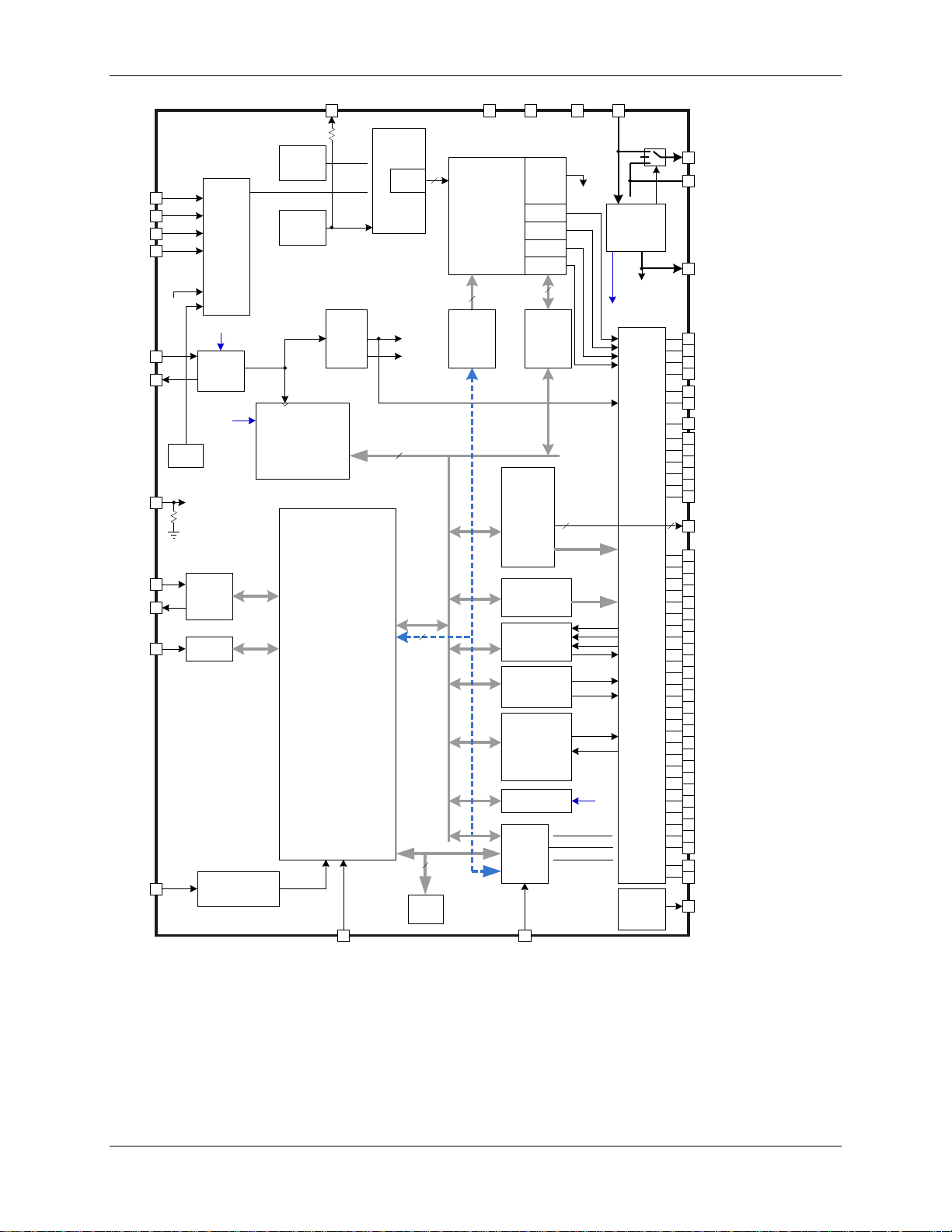
Figure 1: 71M6531D/F IC Functional Block Diagram
8 © 2005-2010 TERIDIAN Semiconductor Corporation v1.3
FDS 6531/6532 005 Data Sheet 71M6531D/F-71M6532D/F
∆Σ ADC
CONVERTER
VREF
ADC_E
MUX
XIN
XOUT
VREF
DIO1/OPT_RX
RESET
V1
UART2--OPTICAL
UART1
TX
RX
4
COM0...3
LCD DISPLAY
DRIVER
DIGITAL I/O
RTCLK (32KHz)
CE_E
RTM_E
POWER FAULT
LCD_E
LCD_CLK
LCD_MODE
DIO
GNDD V3P3A
V3P3D
VBAT
VOLT
REG
2.5V to logic
V2P5
SUM_CYCLES
PRE_SAMPS
EQU
TMUXOUT
FAULTZ
TMUX[4:0]
GNDA
VBIAS
TEMP
SENSOR
OSC
(32KHz)
MCK
PLL
VREF
VREF_DIS
TEST
TEST
MODE
DIO_R
DIO_DIR
E_RXTX
OPT_TXE
RTC
VBIAS
ICE_E
VREF_CAL
RTM_0..3
CE_LCTN
PLS_MAXWIDTH
PLS_INTERVAL
PLS_INV
OPT_TXINV
OPT_TXMOD
OPT_FDC
OPT_RXINV
OPT_RXDIS
LCD_BLKMAP
LCD_SEG
LCD_Y
SLEEP
LCD_ONLY
V3P3SYS
TEST
MUX
VBAT
CE_PROG
CK_CE
CK_MPU
VADC
CE
MULTI-
PURPOSE
IO
MUX_DIV
MUX_ALT
EQU
RTM
RPULSE
WPULSE
COM0..3
SEG...
DIO...
to TMUX
SPI SLAVE
PCMD
EEPROM
EECTRL
FLASH
128KB/
256KB
XRAM
4kB
CE_DATA
PCSZ
PCLK
PSI
PSO
SDATA
SCLK
EEDATA
OPT_TX
OPT_RX
PB
PB
IRAM
256B
MPU
EMULATOR
E_TCLK
E_RSTZ
DIO2/OPT_TX/WPULSE/RPULSE
SEG7/MUX_SYNC
SEG8
SEG9/E_RXTX
SEG10/E_TCLK
SEG11/E_RST
SEG12...SEG18
DIO4/SEG24/SDCK
DIO5/SEG25/SDATA
DIO6/SEG26/WPULSE
DIO7/SEG27/RPULSE
RPULSE
WPULSE
4
XRAM BUS
8
IRAM BUS
8
16
32
22
CKTEST
DIO_PV
DIO_PW
CKOUT_E
MUX_SYNC_E
SPE
DIO_EEX
OPT_TXE
ICE_E
CKOUT_E
SEG0...SEG2
SEG3/PCLK
SEG4/PSDO
SEG5/PCSZ
SEG6/PSDI
FIR
FIR_LEN
VA
IBP
VB
IAP
XPULSE
YPULSE
XPULSE
YPULSE
DIO_PX
DIO_PY
DIO8/SEG28/XPULSE
DIO9/SEG29/YPULSE
SEG19/CKTEST
LCD_DAC
RTCA_ADJ
PREG
QREG
RST_SUBSEC
RTC_SEC
RTC_MIN
RTC_HR
RTC_DAY
RTC_DATE
RTC_MO
RTC_YR
05/26/2010
NVRAM
GP0-GP7
2.5V_NV
2.5V_NV
2.5V_NV
2.5V_NV
IAN
IBN
SEG20...SEG23
DIO10/SEG30...DIO27/SEG47
DIO29/SEG59
DIO30/SEG50
DIO40/SEG60...DIO45/SEG65
DIO47/SEG67...DIO51/SEG71
DIO56...DIO58
DIO3
4
7
3
3
18
6
5
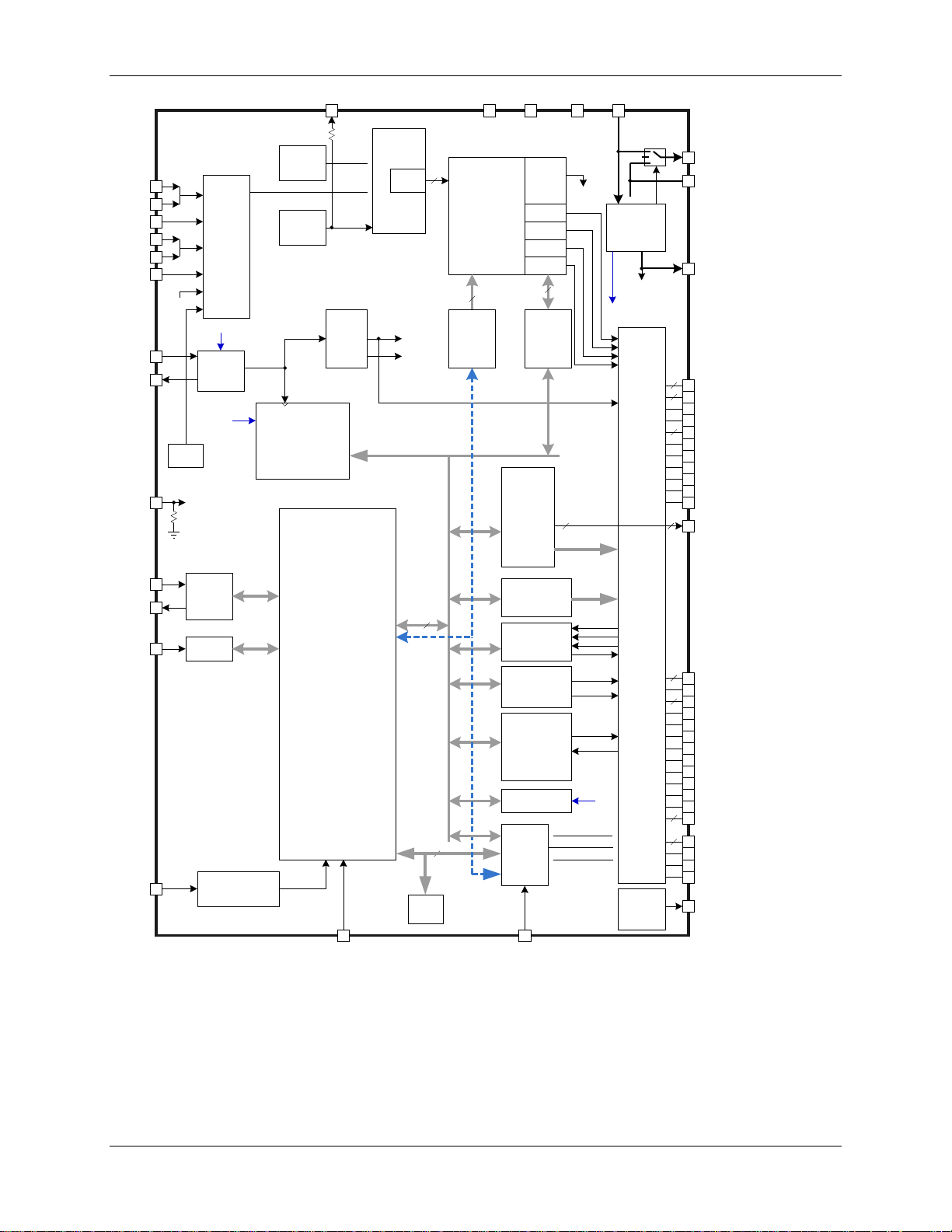
Figure 2: 71M6532D/F IC Functional Block Diagram
v1.3 © 2005-2010 TERIDIAN Semiconductor Corporation 9

Data Sheet 71M6531D/F-71M6532D/F FDS 6531/6532 005
1 Hardware Description
1.1 Hardware Overview
The Teridian 71M6531D/F and 71M6532D/F single-chip energy meters integrates all primary functional
blocks required to implement a solid-state electricity meter. Included on the chips are:
• An analog front end (AFE)
• An Independent digital computation engine (CE)
• An 8051-compatible microprocessor (MPU) which executes one instruction per clock cycle (80515)
• A voltage reference
• A temperature sensor
• LCD drivers
• RAM and Flash memory
• A real time clock (RTC)
• A variety of I/O pins
Various current sensor technologies are supported including Current Transformers (CT), Resistive Shunts
and Rogowski coils.
In a typical application, the 32-bit compute engine (CE) of the 71M6531D/F and 71M6532D/F sequentially
process the samples from the voltage inputs on pins IA, VA, IB, V B and perf orms calculations to measure
active energy (Wh) and reactive energy (VARh), as well as A
These measurements are then accessed by the M PU, processed further and output using the peripheral
devices available to the MPU.
2
h and V2h for four-quadrant metering.
In addition to advanced measurement functions, the real time clock function allows the 71M6531D/F and
71M6532D/F to record time of use (TOU) metering information for multi-rate applications and to time-stamp
tamper events. Measurements can be displayed on 3.3 V LCDs commonly used in low-temperature
environments. Flexible mapping of LCD display segments facilitate integration of existing custom LCDs.
Design trade-off between the number of LCD segments and DIO pins can be implemented in software to
accommodate various requirements.
In addition to the temperature-trimmed ultra-precision voltage reference, the on-chip digital temperature
compensation mechanism includes a temperature sensor and associated controls for correction of unwanted
temperature effects on measurement and RTC accuracy, e.g. to meet the requirements of ANSI and IEC
standards. Temperature-dependent external components such as a crystal oscillator, current transformers
(CTs) and their corresponding signal conditioning circuits can be characterized and their correction factors
can be programmed to produce electricity meters with exceptional accuracy over the industrial temperature
range.
One of the two internal UARTs is adapted to support an Infrared L ED wi th interna l drive and sense
configuration and can also function as a standard UART. The optical output can be modulated at 38 kHz.
This flexibility makes it possible to implement AMR meters with an IR interface. A block diagram of the
71M6531D/F IC is shown in Figure 1. A block diagram of the 71M6532D/F IC is shown in Figure 2.
1.2 Analog Front End (AFE)
The AFE consists of an input multiplexer, a del ta-sigma A/D converter and a voltage reference.
1.2.1 Signal Input Pins
All analog signal input pins are sensitive to voltage. In the 71M6531D/F, the VA and VB pins, as well as the
IA and IB pins are single-ended. In the 71M6532D/F, the IAP/IAN and IBP/IBN pins can be programmed
individually to be differential (see I/O RAM bit SEL_IAN and SEL_IBN) or single-ended. The differential signal
is applied between the IAP and IAN input pins and between the IBP and IBN input pins. Single-ended
signals are applied to the IAP and IBP input pins whereas the common signal, ret urn, is the V3P3A pin.
When using the differential mode, inputs can be chopped, i.e. a connection from V3P3A to IAP or IAN (or
IBP an IBN, respectively) alternates in each multiplexer cycle.
10 © 2005-2010 TERIDIAN Semiconductor Corporation v1.3
FDS 6531/6532 005 Data Sheet 71M6531D/F-71M6532D/F
Regular Slot
Alternate Slot
Address
ADC
Address
ADC
SLOT0_SEL[3:0]
SLOT0_ALTSEL[3:0]
TEMP
SLOT4_SEL[3:0]
SLOT4_ALTSEL[3:0]
SLOT8_SEL[3:0]
SLOT8_ALTSEL[3:0]
1.2.2 Input Multiplexer
The input multiplexer supports up to four input signals that are applied to pins IA (IAP/IAN), VA, IB
(IBP/IBN), and VB of the device. Additionally, using the alternate multiplexer selection, it has the ability to
select temperature and the battery voltage. The multiplexer can be operated in two modes:
• During a normal multiplexer cycle, the signals from the IA (IAP/IAN), IB (IBP/IBN), VA and VB pins
are selected.
• During the alternate multiplexer cycle, t he temperature signal (TEMP) and the battery monitor are
selected, along with some of the voltage and/or current signal sources shown in Table 1. To prevent
unnecessary drainage on the battery, the battery monitor is only active when enabled with the BME
bit (0x2020[6]) in the I/O RAM.
The alternate multiplexer cycles are usually perf ormed infrequently (every second or so) by the MPU. In
order to prevent disruption of the voltage trac king P LL and voltage allpass networks, VA is not replaced in
the ALT selections. Table 1 details the regular and alternative multiplexer sequences. The computation
engine (CE) fills in missing samples due to an ALT multiplexer sequence.
Table 1: Inputs Selected in Regular and Alternate Multiplexer Cycles
Time
Slot
0
1
2
3
–
–
–
–
–
–
The sequence of sampled ch ann els is fully programmable usi ng I/O RAM registers. SLOTn_SEL[3:0]
selects the input for the nth state in a standard mult i plexer frame, while SLOTn_ALTSEL[3:0] selects the
input for the nth state in an alternate multiplexer frame. The states shown in Table 1 are examples for
possible multiplexer state sequences.
In a typical application, IA (IAN/IAP) and IB (IBN/IBP) are connected to current transformers that sense
the current on each phase of the line voltage. VA and VB are typically connected to voltage sensors
through resistor dividers.
Register
SLOT1_SEL[3:0]
SLOT2_SEL[3:0]
SLOT3_SEL[3:0]
SLOT5_SEL[3:0]
SLOT6_SEL[3:0]
SLOT7_SEL[3:0]
SLOT9_SEL[3:0]
Typical Selections
RAM
0 IA
1 VB
2 IB
3 VA
– –
– –
– –
– –
– –
– –
Signal for
Register
SLOT1_ALTSEL[3:0]
SLOT2_ALTSEL[3:0]
SLOT3_ALTSEL[3:0]
SLOT5_ALTSEL[3:0]
SLOT6_ALTSEL[3:0]
SLOT7_ALTSEL[3:0]
SLOT9_ALTSEL[3:0]
Typical Selections
RAM
A
1 VB
B
3 VA
– –
– –
– –
– –
– –
– –
Signal for
VBAT
The multiplexer control circuit (MUX_CT RL signal) controls multiplexer advance, FIR initiation and VREF
chopping. Additionally, MUX_CTRL laun ches each pass through the CE program. Conceptually,
MUX_CTRL is clocked by CK32, the 32768 Hz clock from the PLL bloc k. T he behavior of MUX_CTRL is
governed by MUX_ALT, EQU[2:0], CHOP_E[1:0] and MUX_DIV[3:0].
The MUX_ALT bit requests an alternative multiplexer frame. The bit may be ass ert ed on any MPU cycle
and may be subsequently de-asserted on any cycle including the next one. A rising edge on MUX_ALT
will cause MUX_CTRL to wait until the next multiplexer frame and implement a single alternate multiplexer
frame.
Another control input to the MUX is MUX_DIV[3:0]. These four bits can request from 1 to 10 multiplexer
states per frame. The multiplexer always starts at the beginning of its list and proceeds until the number
of states defined by MUX_DIV[3:0] hav e been convert ed.
v1.3 © 2005-2010 TERIDIAN Semiconductor Corporation 11
Data Sheet 71M6531D/F-71M6532D/F FDS 6531/6532 005
Address (HEX)
Name
Address (HEX)
Name
The duration of each multiplexer state depends on the number of ADC samples processed by the FIR,
which is set by FIR_LEN[1:0]. Each multiplexer state will start on the rising edge of CK32. The MUX_CTRL
signal sends an FIR_START command to begin t he calculation of a sample value from the ADC bit
stream by the FIR. Upon receipt of the FIR_DONE signal from the FIR, the mul tiplexer will wait until the
next CK32 rising edge to increment its state and ini tiate the next FIR conversion. FIR conversi ons require
1, 2, or 3 CK32 cycles. The number of CK32 cycles i s det ermined by FIR_LEN[1:0], as shown in Table 2.
1.2.3 A/D Converter (ADC)
A single delta-sigma A/D converter digitizes the voltage and current inputs to the 71M6531D/F and
71M6532D/F. The resolution of the ADC is programmable using the I/O RAM M40MHZ and M26MHZ bits
(see Table 2). The CE code must be tailored for use with the selected ADC r esolution.
Table 2: ADC Resolution
Setting for
[M40MHZ, M26MHZ]
[00], [10] or [11]
[01]
FIR_LEN[1:0]
0
1
2
0
1
2
CK32
Cycles
1
2
3
1
2
3
FIR CE Cycles Resolution
138
288
384
186
384
588
18 bits
21 bits
22 bits
19 bits
22 bits
24 bits
Initiation of each ADC conversion is controlled by M UX_CTRL as described above. At the end of each
ADC conversion, the FIR filter output data is st ored into the CE RAM location determine d by the MUX
selection.
1.2.4 FIR Filter
The finite impulse response filter is an integral part of the ADC and it is optimized for use with the multiplexer.
The purpose of the FIR filter is to decimate the ADC output to the desired resolution. At the end of each
ADC conversion, the output data is stored into the fixed CE RAM location determined by the m ul tiplexer
selection as shown in Table 3. FIR data is stored LSB justi fied, but shifted left by eight bits.
Table 3: ADC RAM Locations
0x00 IA 0x09 AUX
0x01 VB 0x0A TEMP
0x02 IB 0x0B VBAT
0x03 VA
1.2.5 Voltage References
The device includes an on-chip precision bandgap voltage reference that incorporates auto-zero techniques.
The reference is trimmed to minimize errors c aused by component mismatch and drift. The result is a
voltage output with a predictable temperature c oefficient.
The amplifier within the reference is chopper stabilized, i.e. the polarity can be switched by the MPU using
CHOP_E[1:0] (IORAM 0x2002[5:4]). The CHOP_E[1:0] field enables the MPU to operate the chopper circuit
in regular or inverted operation, or in toggling mode. When the chopper circuit is toggled in between
multiplexer cycles, DC offsets on the measured sig nals will automatically be averaged out.
The general topology of a chopped amplifier is shown in Figure 3.
12 © 2005-2010 TERIDIAN Semiconductor Corporation v1.3
FDS 6531/6532 005 Data Sheet 71M6531D/F-71M6532D/F
G
-
+V
inp
V
outp
V
outn
V
inn
CROSS
A
B
A
B
A
B
A
B
Mult iplexer fram es
Accumu lati on int erval n Accumul ation inter val n+1
2 43 251925201 2 43 251925201
Alt ernati ve MUX cy cle
Mult iplexer fram es
Alt ernati ve MUX cy cle
CROSS CROSS
Figure 3: General Topology of a Chopped Amplifier
It is assumed that an offset voltage Voff appears at the positive amplifier input. W ith all sw itches , as
controlled by CROSS, in the A position, the output voltage is:
Voutp – Voutn = G (Vinp + Voff – Vinn) = G (Vinp – V i nn) + G Voff
With all switches set to the B position by applying the inverted CROSS signal, the output voltage is:
Voutn – Voutp = G (Vinn – Vinp + Voff) = G (Vinn – Vinp) + G Voff, or
Voutp – Voutn = G (Vinp – Vinn) - G Voff
Thus, when CROSS is toggled, e.g. after each multiplexer cycle, the offset will alternately appear on the
output as positive and negative, which results in the offset effectively being eliminated, regardless of i ts
polarity or magnitude.
When CROSS is high, the connection of the amplifier input devices is reversed. This preserves the overall
polarity of that ampl if ier gain; it in ve r ts its i npu t o ffset . By alternately reversing the connection, the
amplifier’s offset is averaged to zero. This rem oves the most significant long-term drift mechanism in the
voltage reference. The CHOP_E[1:0] field controls the behavior of CROSS. The CROSS signal will reverse
the amplifier connection in the voltage reference in or der to negate the effects of its offset. On the first
CK32 rising edge after the last multiplexe r st ate of its sequence, the multiplexer will wait one additional
CK32 cycle before beginning a new frame. At the beginning of this cycle, the value of CROSS will be
updated according to the CHOP_E[1:0] field. The extra CK32 cycle allows time for the chopped VREF to
settle. During this cycle, MUXSYNC is held high. The leading edge of MUXSYNC initiates a pass
through the CE program sequence. The begin ni ng of the sequence is the serial readout of the four RT M
words.
CHOP_E[1:0] has four states: positive, reverse and two toggle states. In the positiv e state, CHOP_E[1:0]
= 01, CROSS and CHOP_CLK are held low. In the reverse state, CHOP_E[1:0] = 10, CROSS and
CHOP_CLK are held high. In the first toggle state, CHOP_E[1:0] = 00, CROSS is automatically toggled
near the end of each multiplexer frame and an ALT frame is forced during the last multiplexer frame in each
SUM cycle. It is desirable that CROSS take on alternate values during each ALT frame. For this reason,
if CHOP_E[1:0] = 00, CROSS will not toggle at the en d of the multiplexer frame immediately preceding
the ALT frame in each accumulation interval.
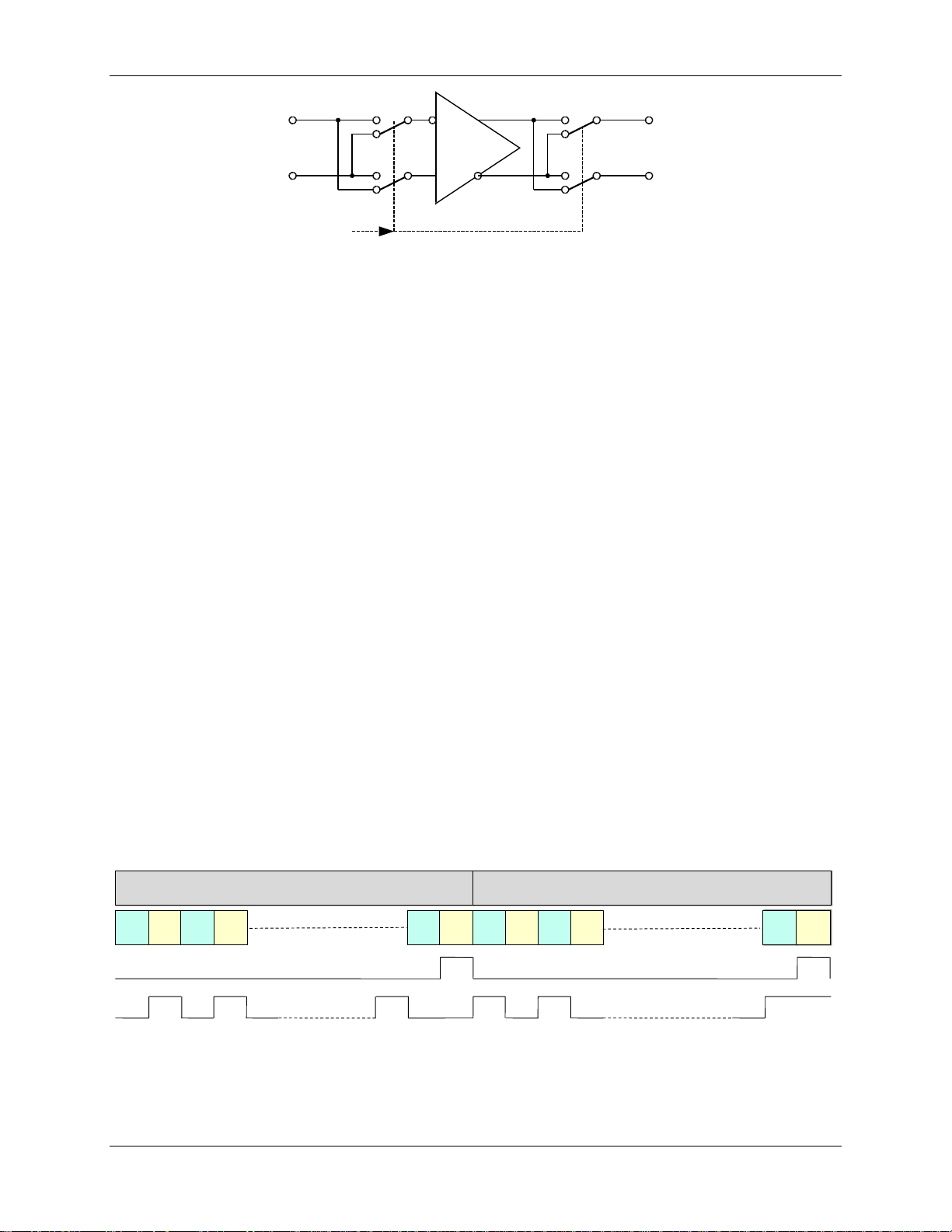
Figure 4 shows CROSS over two accumulation int erval when CHOP_E[1:0] = 00: At the end of the first
interval, CROSS is low, at the end of the second interval, CROSS is high. The offset error for the two
temperature measurements taken during the ALT multiplexer frames will be averaged to zero. Note that
v1.3 © 2005-2010 TERIDIAN Semiconductor Corporation 13
Figure 4: CROSS Signal with CHOP_E[1:0] = 00
Data Sheet 71M6531D/F-71M6532D/F FDS 6531/6532 005
∆Σ ADC
CONVERTER
VREF
ADC_E
MUX
VREF
VBIAS
VREF
VREF_DIS
VBIAS
VREF_CAL
VBAT
VADC
MUX_DIV
MUX_ALT
EQU
22
FIR
FIR_LEN
VA
IBP
VB
IAP
IAN
IBN
TEMP
SENSOR
the number of multiplexer frames in an accumulation interval is always even. Operation with
CHOP_E[1:0] = 00 does not require control of the chopping mechanism by the MPU while eliminating the
offset for temperature measurement.
In the second toggle state, CHOP_E[1:0] = 11, no ALT frame is forced during the last multiplexer cy cle i n
an accumulation interval and CROSS always toggles near the end of each multiplexer frame.
The internal bias voltage, VBIAS (typically 1.6 V), is used by the ADC when measuring the tem perature
and battery monitor signals.
1.2.6 Temperature Sensor
The 71M6531D/F and 71M6532D/F include an on-chip temperature sensor implemented as a bandgap
reference. It is used to determine the die t em perature. The MPU may request an alternate multiplexer
cycle containing the temperature sensor output by asserting MUX_ALT.
The primary use of the temperature dat a i s to determine the magnitude of compensation req uired to offset
the thermal drift in the system (see Section 3.4 Temperature Compens ation).
1.2.7 Battery Monitor
The battery voltage is measured by the ADC during alternative multiplexer frames if the BME (Battery
Measure Enable) bit in the I/O RAM is set. While BME is set, an on-chip 45 kΩ load resistor is applied to
the battery and a scaled fraction of the batt ery voltage is applied to the ADC input. After each alternative
MUX frame, the result of the ADC conversion is avail able at XRAM address 0x0B. BME is ignored and
assumed zero when system power is not available (V1 < VBIAS). See Section 5.4.4 Battery Monitor.
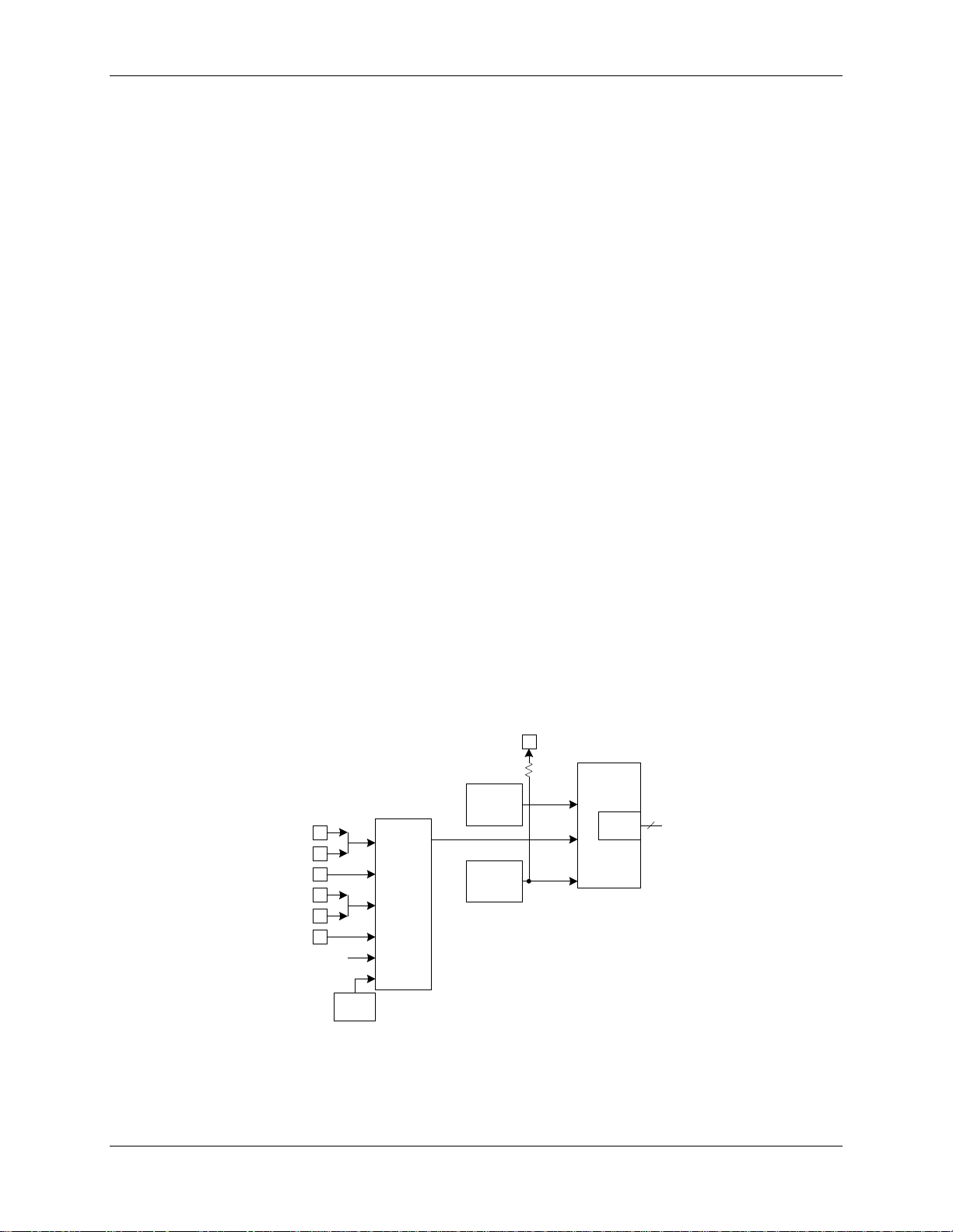
1.2.8 AFE Functional Description
The AFE functions as a data acquisition system, controlled by the MPU. The main signals (IA, VA, IB and
VB) are sampled, and the ADC counts obtained are store d in X RAM where they can be accessed by the
CE and, if necessary, by the MPU. Alternate mul tiplexer cycles are initiated less frequently by the MPU to
gather access to the slow temperature and bat tery signals.
Figure 5 shows the block diagram of the AFE , with current inputs shown only as differential pair of pin s
(for the 71M6531D/F, the current input for phase A is a single pin [IA]).
Figure 5: AFE Block Diagram (Shown for the 71M6532D/F )
14 © 2005-2010 TERIDIAN Semiconductor Corporation v1.3

FDS 6531/6532 005 Data Sheet 71M6531D/F-71M6532D/F
Address (HEX)
Name
Description
1.3 Digital Computation Engine (CE)
The CE, a dedicated 32-bit signal processor, performs the precision computations necessary to accurately
measure energy. The CE calculations and proces ses include:
• Multiplication of each current sample with its as sociated voltage sample to obtain the energy per
sample (when multiplied with the constant sampl e time).
• Frequency-insensitive delay cancellation on all four channels (to compensate for t he del ay between
samples caused by the multiplexing scheme).
• 90° phase shifter (for VAR calculations).
• Pulse generation.
• Monitoring of the input signal frequency (f or frequency and phase information).
• Monitoring of the input signal amplitude ( for sag detection).
• Scaling of the processed samples based on calibrat ion coefficients.
• Scaling of all samples based on temperature compensation information (71M6532D/F only).
The CE program resides in flash memory. Common access to flash memory by CE and MPU is controlled
by a memory share circuit. Each CE instruction word is two bytes long. Allocated flash space for the CE
program cannot exceed 4096 16-bit words (8 KB). The CE progra m count er begins a pass through the
CE code each time multiplexer state 0 begins. The code pass ends when a HALT instruction is executed.
For proper operation, the code pass must be completed before the multiplexer cycle ends (see Section
2.2 System Timing Summary).
The CE program must begin on a 1-KB boundary of the flash address. The I/O RAM register CE_LCTN[7:0]
defines which 1-KB boundary contains the CE cod e. Thus, the first CE instruction is located at
1024*CE_LCTN[7:0].
The CE can access up to 4 KB of data RAM (XRAM), or 1024 32-bit data words, starting at RAM addres s
0x0000.
The XRAM can be accessed by the FIR filter block, the RTM circuit, the CE, and the MPU. Assigned time
slots are reserved for FIR, and MPU, respectively, to prevent bus contention for XRAM data access.
The MPU can read and write the XRAM as the primary means of data communication between the two
processors. Table 4 shows the CE addresses in XRAM allocated to analog inputs from the AFE.
Table 4: XRAM Locations for ADC Results
0x00 IA Phase A current
0x01 VA Phase A voltage
0x02 IB Phase B current
0x03 VB Phase B voltage
0x04...0x09 – Not used
0x0A TEMP Temperature
0x0B VBAT Battery Voltage
The CE is aided by support hardware to facilita te implemen tation o f equa tions, pu lse co unters and
accumulators. This hardware is controlled through I/O RAM locati ons EQU[2:0] (equation assist), the
DIO_PV and DIO_PW (pulse count assist) bits and PRE_SAMPS[1:0] and SUM_CYCLES[5:0] (accumulation
assist).
PRE_SAMPS[1:0] and SUM_CYCLES[5:0] support a dual level accumula tion sc heme where the firs t
accumulator accumulates results from PRE_SAMPS[1:0] samples and the second accumulator accumulates
up to SUM_CYCLES[5:0] of the first accumulator results. The integration time for each energy output is
PRE_SAMPS[1:0] * SUM_CYCLES[5:0]/2520.6 (with MUX_DIV[3:0] = 1). The CE hardware issues the
XFER_BUSY interrupt when the accumulation is c om plete.
v1.3 © 2005-2010 TERIDIAN Semiconductor Corporation 15
Data Sheet 71M6531D/F-71M6532D/F FDS 6531/6532 005
2
1 element, 2 W,
current sense
1 element, 3 W,
2 element, 3 W,
3φ Delta
1.3.1 Meter Equations
The 71M6531D/F and 71M6532D/F provide hardware assistance to the CE in order to support various
meter equations. This assistance is controll ed through I/O RAM location EQU[2:0] (equation assist). The
Compute Engine (CE) firmware for residential configurations implements the equations listed in Table 5.
EQU[2:0] specifies the equation to be used based on the number of phases used for meteri ng.
Table 5: Meter Equations
EQU[2:0] Description
0
1
2
Not all CE codes support all equations.
1φ with neutral
1φ
Element 0 Element 1 Element
VA · IA VA · IB N/A
VA(IA-
VA · IA VB · IB N/A
Watt and VAR Formula
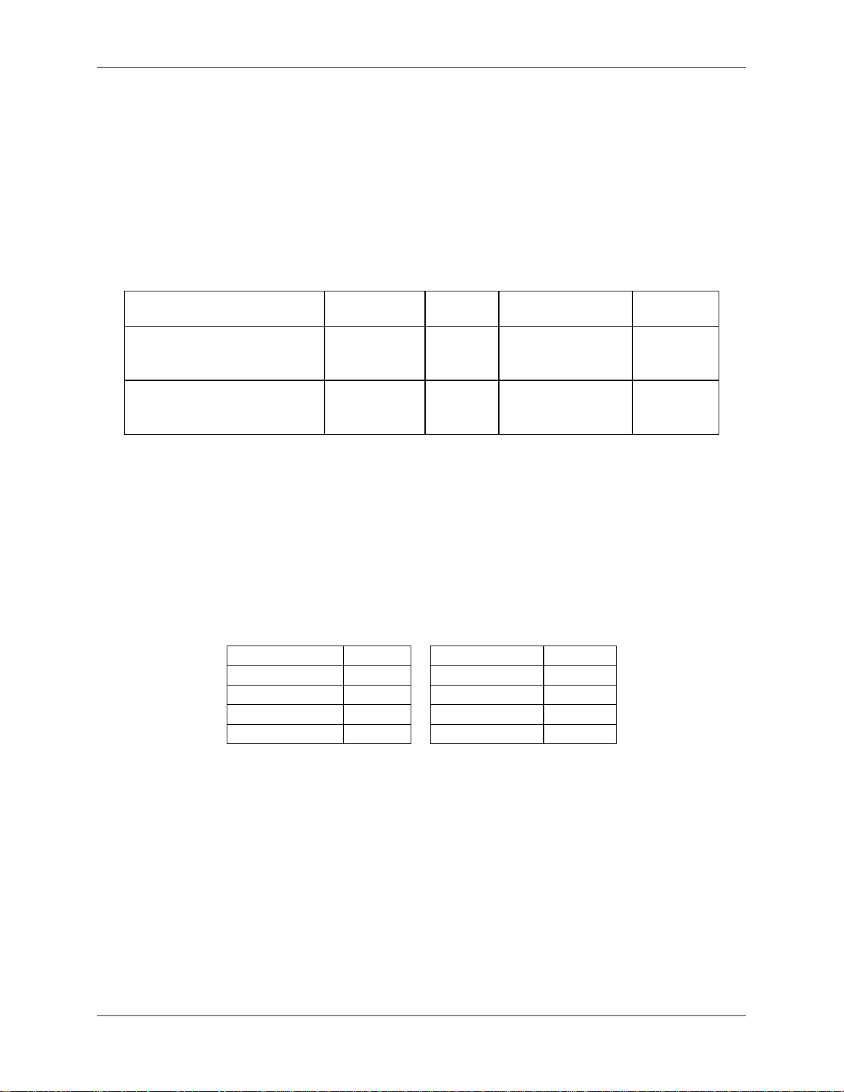
IB)/2
N/A N/A
Mux
Sequence
Sequence is
programmable
with
SLOTn_SEL[3:0]
ALT Mux
Sequence
Sequence is
programmable with
SLOTn_ALTSEL[3:0]
1.3.2 Real-Time Monitor
The CE contains a Real-Time Monitor (RTM), which can be programmed to monitor four selectable XRAM
locations at full sample rate. The four monitored locations are serially output to the TMUXOUT pin via the
digital output multiplexer at the beginning of each CE code pass. The RTM can be enabled and disabled
with the RTM_E bit. The RTM output is clocked by CKTEST (pin SEG19/CKTEST), with the clock output
enabled by setting CKOUT_E = 1. Each RTM word is clocked out in 35 cycles and contains a leading flag
bit. See Figure 20 for the RTM output format. RTM is low when not in use.
1.3.3 Pulse Generators
The 71M6531D/F and 71M6532D/F provide four pulse generators, RPULSE, WPULSE, XPULSE and
YPULSE, as well as increased hardware support for the two original pulse generators (RPULSE and
WPULSE). The pulse generators can be used to output CE status indicators, SAG for example, to DIO pins.
The polarity of the pulses may be inverted with the PLS_INV bit. When this bit is set, the pul ses are active
high, rather than the more usual active low. PLS_INV inverts all the pulse output s.
XPULSE and YPULSE
Pulses generated by the CE may be exported to t he XPULSE and YPULSE pulse outputs. Pins DIO8
and DIO9 are used for these pulses. Generally, t he XPULSE and YPULSE outputs are updated once on
each pass of the CE code, resulting in a pulse f requency up to a maximum of 1260Hz (assuming a MUX
frame is 13 CK32 cycles).
The YPULSE pin can be used by the CE code to generate i nterrupts based on sag events. This method
is faster than checking the sag bits by the MPU at every CE_BUSY interrupt. See Section 4.3.6 CE Status
and Control for details.
RPULSE and WPULSE
During each CE code pass, the hardware stores ex ported WPULSE AND RPULSE sign bits in an 8-bit
FIFO and outputs them at a specified interval. This permits the CE code to calculate the RPULSE and
WPULSE outputs at the beginning of its code pass a nd to rely on hardware to spread them over the MUX
frame. The FIFO is reset at the beginning of each MUX frame. The PLS_INTERVAL register controls the
delay to the first pulse update and the interv al between subsequent updates. Its LSB is 4 CK_FIR cycles.
If zero, the FIFO is deactivated and the DFF s are updated immediately. Thus, N
4 * PLS_INTERVAL.
16 © 2005-2010 TERIDIAN Semiconductor Corporation v1.3
INTERVAL is

FDS 6531/6532 005 Data Sheet 71M6531D/F-71M6532D/F
o
delay
o
delay
ft
T
t
360360 ⋅⋅=⋅=
φ
Since the FIFO resets at the beginning of each MUX frame, the user must specify PLS_INTERVAL so that
all of the pulse updates are output
before
the MUX frame completes. For instance, if the CE code outputs
5 updates per MUX interval and if the MUX int erval is 1950 cycles long, the ideal value for the interval i s
1950/5/4 = 97.5. If PLS_INTERVAL = 98, the fifth output will occur too late and be lost. In this case, the
proper value for PLS_INTERVAL is 97.
Hardware also provides a maximum pulse width feature. The PLS_MAXWIDTH register selects a maximum
negative pulse width to be Nmax updates according to the formula: Nmax = (2*PLS_MAXWIDTH+1). If
PLS_MAXWIDTH = 255, no width checking is performed.
The WPULSE and RPULSE pulse generator outputs are available on DIO6 and DIO7, respectively. They
can also be output on OPT_TX (see OPT_TXE[1:0] for details).
1.3.4 Data RAM (XRAM)
The CE and MPU use a single general-purpose Data RAM (also referred to as XRAM). The Data RAM is
1024 32-bit words, shared between the CE and the MPU using a time-multiplex method. This reduces
MPU wait states when accessing CE data. When the MPU and CE are clocking at maximum frequency
(10 MHz), the DRAM will make up to four accesses during each 100 ns interval. These consist of two
MPU accesses, one CE access and one SPI access.
The Data RAM is 32 bits wide and uses an ext ernal multiplexer so as to appear byte-wide to the MPU.
The Data RAM hardware will convert an MPU byte write operation into a read-modify-write operation that
requires two Data RAM accesses. The second ac cess is guaranteed to be available because the MPU
cannot access the XRAM on two consecutive instructions unless it is using the same address.
In addition to the reduction of wait states, t hi s arr angement permits the MPU to easily use unneeded CE
data memory. Likewise, the amount of memory the CE uses is not limited by the size of a dedicated CE
data RAM.
1.3.5 Delay Compensation
When measuring the energy of a phase (i.e., Wh and VARh) in a service, the voltage and current for that
phase must be sampled at the same instant. Otherwise, the phase difference, Ф, introduces errors.
Where f is the frequency of the input signal and t
is the sampling delay between voltage and current.
delay
In traditional meter ICs, sampling is accomplished by using two A/ D converters per phase (one for voltage
and the other one for current) controlled to sample simultaneously. Teridian’s patented Single-Converter
Technology
®
, however, exploits the 32-bit signal processi ng capability of its CE to implement “constant
delay” all-pass filters. These all-pass filters correct for the conversion time difference between the voltage
and the corresponding current samples that are obtained with a single multiplexed A/D converter.
The “constant delay” all-pass filters provide a broad-band delay β, that is precisely matched to the differ-
ence in sample time between the voltage and the current of a given phase. This digital filter does not affect the amplitude of the signal, but provi des a precisely controlled phase response. The delay compensation implemented in the CE aligns the voltage samples with their corresponding current samples by
routing the voltage samples through the all-pass filter, thus delaying the voltage samples by β, resulting in
the residual phase error β – Ф. The residual phase error is negligible, and is typically less than ±1.5 m il l idegrees at 100Hz, thus it does not contribute to errors in the energy measurements.
1.3.6 CE Functional Overview
The ADC processes one sample per channel per mul tiplexer cycle. Figure 6 shows the timing of the
samples taken during one multiplexer cycle.
The number of samples processed during one a ccumulation cycle is controlled by PRE_SAMPS[1:0]
(IORAM 0x2001[7:6]) and SUM_CYCLES[5:0] (IORAM 0x2001[5:0]). The integration time for each energy
output is:
PRE_SAMPS[1:0] * SUM_CYCLES[5:0] / 2520.6, where 2520.6 is the sample rate [Hz]
v1.3 © 2005-2010 TERIDIAN Semiconductor Corporation 17
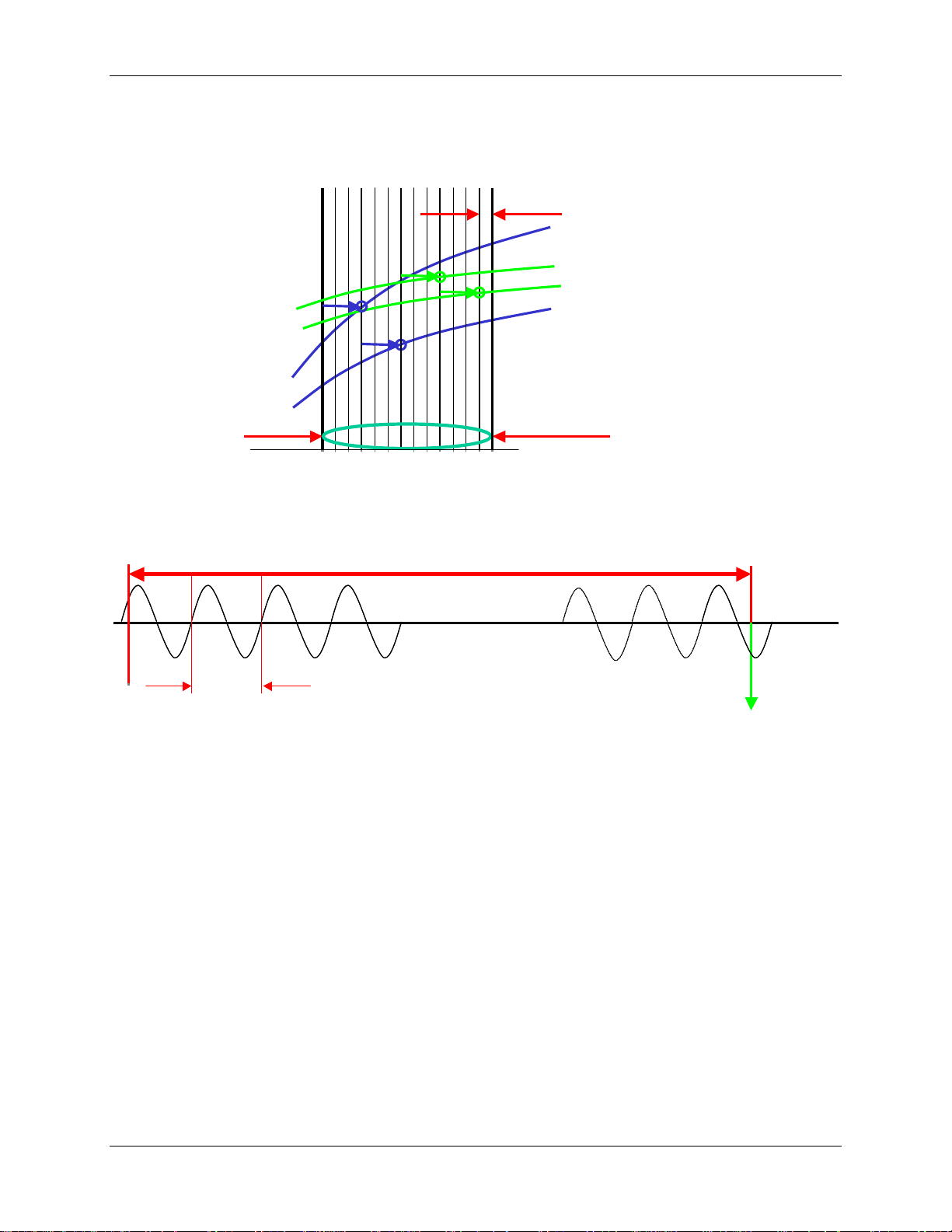
Data Sheet 71M6531D/F-71M6532D/F FDS 6531/6532 005
VA
IA
1/32768Hz =
30.518µs
13/32768Hz = 397µs
per mux cycle
IB
VB
XFER_BUSY
Interrupt to MPU
20ms
833ms
For example, PRE_SAMPS[1:0] = 42 and SUM_CYCLES[5:0] = 50 will establish 2100 sampl es per accumulati on
cycle. PRE_SAMPS[1:0] = 100 and SUM_CYCLES[5:0] = 21 will result in the exact same accumulation
cycle of 2100 samples or 833 ms. After an accumulation cycle is completed, the XFER_BUSY interrupt
signals to the MPU that accumulated data are av ai l able.
Figure 6: Samples from Multiplexer Cycle
The end of each multiplexer cycle is signaled to the MPU by the CE_BUSY interrupt. At the end of each
multiplexer cycle status information, such as sag data and the digitized input signal, is available to the MPU.
Figure 7: Accumulation Interval
Figure 7 shows the accumulation interval resulting from PRE_SAMPS[1:0] = 42 and SUM_CYCLES[5:0] =
50, consisting of 2100 samples of 397 µs each, followed by the XFER_BUSY interrupt. The sampling in
this example is applied to a 50 Hz signal.
There is no correlation between the line signal frequency and the choice of PRE_SAMPS[1:0] or
SUM_CYCLES[5:0] (even th ough when SUM_CYCLES[5:0] = 42 one set of SUM_CYCLES[5:0] happens to
sample a period of 16.6 ms). Furthermore, sampling does n ot have to start when the line voltage crosses
the zero line and the length of the accumulation interval need not be an integer multiple of the signal cycles.
18 © 2005-2010 TERIDIAN Semiconductor Corporation v1.3

FDS 6531/6532 005 Data Sheet 71M6531D/F-71M6532D/F
M40MHZ, M26MHZ
1.4 80515 MPU Core
The 71M6531D/F and 71M6532D/F include an 80515 MPU (8-bit, 8051-compatible) that processes most
instructions in one clock cycle. Using a 10-MHz clock results in a processing throughput of 10 MIPS. The
80515 architecture eliminates redundant bus states and implements parallel execution of fetch and execution
phases. Normally, a machine c ycle i s alig ned wit h a memory fetch, therefore, most of the 1-byte instructions
are performed in a single machine cycle (MPU clock cycle). This leads to an 8x average performance
improvement (in terms of MIPS) over the Intel
Table 6 shows the CKMPU frequency as a f unct ion of the allowed combinations of the MPU clock divi der
MPU_DIV[2:0] and the MCK divider bits M40MHZ and M26MHZ. Actual processor clocking speed can be
adjusted to the total processing demand of the application (metering calculations, AMR management, memory management, LCD driver management and I/ O m anagement) using the I/O RAM field MPU_DIV[2:0]
and the MCK divider bits M40MHZ and M26MHZ, as shown in Table 6.
Table 6: CKMPU Clock Frequencies
MPU_DIV [2:0]
000 9.8304 MHz 6.5536 MHz 4.9152 MHz
001 4.9152 MHz 3.2768 MHz 2.4576 MHz
010 2.4576 MHz 1.6384 MHz 1.2288 MHz
011 1.2288 MHz 819.2 kHz 614.4 kHz
100 614.4 kHz 409.6 kHz 307.2 kHz
101 307.2 kHz 204.8 kHz 153.6 kHz
110 153.6 kHz 102.4 kHz 76.80 kHz
111 153.6 kHz 102.4 kHz 76.8 kHz
Typical measurement and metering functions based on the results provided by the internal 32-bit compute
engine (CE) are available for the MPU as part of Teridian’s standard library. Teridian provides demonstration
source code to help reduce the design cycle.
8051 device running at the same clock frequency.
[
] Values
[1,0] [0,1] [0,0]
1.4.1 Memory Organization and Addressing
The 80515 MPU core incorporates the Harvard architecture with separate code and data spaces. Memory
organization in the 80515 is similar to that of the industry standard 8051. There are four memory areas:
Program memory (Flash, shared by MPU and CE), external RAM (Data RAM, shared by the CE and MPU,
Configuration or I/O RAM), and internal data memory (Internal RAM). Table 7 shows the memory map.
Program Memory
The 80515 can address up to 64 KB of program memory space from 0x0000 to 0xFFFF. Program memory
is read when the MPU fetches instructions or p erforms a MOVC operation. Access to program memory
above 0x7FFF is controlled by the FL_BANK[2:0] register (SFR 0xB6).
After reset, the MPU starts program execution from program memory location 0x0000. The lower part of
the program memory includes reset and interrupt vectors. Th e interrupt vectors are spaced a t 8-byte
intervals, starting from 0x0003.
MPU External Data Memory (XRAM )
Both internal and external memory is physically located on the 71M6531 d evice. The external memory
referred to in this documentation is only external to the 80515 MPU core.
4 KB of RAM starting at address 0x0000 is shared by the CE and MPU. The CE normally uses the first
1 KB, leaving 3 KB for the MPU. Different versions of the CE code use varying amounts. Consult the
documentation for the specific code version being used for the exact limit.
If the MPU overwrite s th e CE’s worki ng RA M, the CE’s output may b e co rrupte d. If t he CE is disa bled,
the first 0x40 bytes of RAM are still unu sable while MUX_DIV[3:0] ≠ 0 because the 71M6531 ADC
writes to these locations. Setting MUX_DIV[3:0] = 0 disabl es th e ADC output prev entin g the CE from
writing the first 0x4 0 byte s of RA M.
v1.3 © 2005-2010 TERIDIAN Semiconductor Corporation 19
Data Sheet 71M6531D/F-71M6532D/F FDS 6531/6532 005
(hex)
Technology
Type
(bytes)
KB boundary)
The 80515 writes into external data memory when the MPU executes a MOVX @Ri,A or MOVX
@DPTR,A instruction. The MPU reads ext ernal data memory by executing a MOVX A,@Ri or MOVX
A,@DPTR instruction (SFR PDATA provides the upper 8 bytes for the MOVX A,@Ri instruction).
Internal and External Memory Map
Table 7 shows the address, type, use and size of the various memory components.
Only the memory ranges shown in Table 7 contain physical memory.
Table 7: Memory Map
Address
Memory
Memory
Name Typical Usage
Memory Size
00000-1FFFF/
00000-3FFFF
Flash
Memory
Non-volatile
0000-0FFF Static RAM Volatile
2000-20BF,
20C8-20FF
20C0-20C7 Static RAM
Static RAM Volatile
Non-volatile
(battery)
Program memory
for MPU and CE
External RAM
(XRAM)
Configuration RAM,
I/O RAM
Configuration RAM,
I/O RAM
MPU Program and
non-volatile data
CE program (on 1
Shared by CE and
MPU
Hardware control 256
Battery-buffered
memory
128 KB/
256 KB
†
8 KB max.
4 KB
8
0000-00FF Static RAM Volatile Internal RAM Part of 80515 Core 256
†
Memory size depends on the IC. See Section1.5.5 Physical Memory for details.
MOVX Addressing
There are two types of instructions differing in whether they provide an 8-bit or 16-bit indirect address to
the external data RAM.
In the first type, MOVX A,@Ri, the contents of R0 or R1 in the current register bank provi de the eight
lower-ordered bits of address. The eight high-ordered bits of the address are specified with the PDATA
SFR. This method allows the user paged access (256 page s of 256 bytes each) to all ranges of the
external data RAM.
In the second type of MOVX instruction, MOVX A,@DPTR, the data pointer generates a 16-bit address.
This form is faster and more efficient when accessing very large data arrays (up to 64 KB), since no
additional instructions are needed to set up the eight high ordered bits of the address.
It is possible to mix the two MOVX types. This provides the user with four sep arate data pointers, two
with direct access and two with paged access, to the entire 64 KB of external memory range.
Dual Data Pointer
The Dual Data Pointer accelerates the block mov es of data. The standard DPTR is a 16-bit register that
is used to address external memory or peripheral s. In the 80515 core, the standard data pointer is called
DPTR, the second data pointer is called DPTR1. The data pointer select bit, located in the LSB of the DPS
register (DPS[0]), chooses the active pointer. DPTR is select ed when DPS[0] = 0 and DPTR1 is selected
when DPS[0] = 1.
The user switches between pointers by toggling the LSB of the DPS register. The values in the data pointers
are not affected by the LSB of the DPS register. All DPTR relat ed instructions use the currently selected
DPTR for any activity.
The second data pointer may not be supported by certain compilers.
DPTR1 is useful for copy routines, where it can make t he inner loop of the routine t wo instructions faster
compared to the reloading of DPTR from registers. Any interrupt routine using DPTR1 must save
and restore DPS, DPTR and DPTR1, which increases stack usage and slows down interrupt latency.
By selecting the Evatronics R80515 core in the Kei l compi l er project settings and by using the
compiler directive “MODC2”, dual d ata point ers are enabled in certain library routines.
20 © 2005-2010 TERIDIAN Semiconductor Corporation v1.3
FDS 6531/6532 005 Data Sheet 71M6531D/F-71M6532D/F
Addressable
X000
X001
X010
X011
X100
X101
X110
X111
F8
INTBITS
FF
F0
F7
D8
WDCON
DF
D0
D7
B8
IEN1
IP1
S0RELH
S1RELH
PDATA
BF
B0
B7
98
S0CON
S0BUF
IEN2
S1CON
S1BUF
S1RELL
EEDATA
EECTRL
9F
90
97
An alternative data pointer is available in the form of the PDATA register (SFR 0xBF), sometimes referred
to as USR2). It defines t he hi gh byt e of a 16-bit address when reading or writing XDATA with the instruction
MOVX A,@Ri or MOVX @Ri,A.
Internal Data Memory Map and Access
The Internal data memory provides 256 bytes (0x00 to 0xFF) of data memory. The internal data memory
address is always 1 byte wide. Table 8 shows the internal data memory map.
The Special Function Registers (SFR) occupy the upper 128 bytes. The SFR area of internal data memory
is available
only by direct addressing
. Indirect addressing of this area accesses the upper 1 28 bytes of
Internal RAM. The lower 128 bytes contain working registers and bit addressable memory. The lower 32
bytes form four banks of eight registers (R0-R7). Two bits on the program memory status word (PSW) select
which bank is in use. The next 16 bytes form a block of bit addressable memory space at bit addresses
0x00-0x7F. All of the bytes in the lower 128 bytes are accessible through direct or indirect addressing.
Table 8: Internal Data Memory Map
Address Range Direct addressing Indirect addressing
0x80 0xFF Special Function Registers (SFRs) RAM
0x30 0x7F Byte addressable area
0x20 0x2F Bit addressable area
0x00 0x1F Register banks R0…R7
1.4.2 Special Function Registers (SFRs)
A map of the Special Function Registers is show n i n Table 9.
Only a few addresses in the SFR memory space are occupied, the others are not implemented. A read
access to unimplemented addresses will return undefined data, while a write access will have no effect.
SFRs specific to the 71M6531D/F and 71M6532D/F are shown in bold print on a gray field. The registers
at 0x80, 0x88, 0x90, etc., are bit addressable, all others are by te addressable. See the restrictions for the
INTBITS register in Table 14.
Table 9: Special Function Register Map
Hex/
Bin
Bit
Byte Addressable
Bin/
Hex
B
E8 IFLAGS
E0
A
EF
E7
PSW
C8
C0
A8
A0 P2 DIR2 DIR0
T2CON
IRCON
P3
FLSHCTL
FL_BANK PGADR
IEN0 IP0 S0RELL
CF
C7
AF
A7
88
80
P1 DIR1
DPS
ERASE
TCON TMOD TL0 TL1 TH0 TH1 CKCON
P0 SP DPL DPH DPL1 DPH1 PCON
8F
87
v1.3 © 2005-2010 TERIDIAN Semiconductor Corporation 21

Data Sheet 71M6531D/F-71M6532D/F FDS 6531/6532 005
1.4.3 Generic 80515 Special Function Registers
Table 10 shows the location, description and reset or power-up value of the generic 80515 SFRs. Additional
descriptions of the registers can be found at the page num bers listed in the table.
Table 10: Generic 80515 SFRs - Location and Reset Values
Name
P0
SP
DPL
DPH
DPL1
DPH1
PCON
TCON
TMOD
TL0
TL1
TH0
TH1
CKCON
P1
DPS
S0CON
S0BUF
IEN2
S1CON
S1BUF
S1RELL
P2
IEN0
IP0
S0RELL
P3
IEN1
IP1
S0RELH
S1RELH
PDATA
IRCON
T2CON
PSW
WDCON
A
B
Address
(Hex)
0x80 0xFF Port 0 24
0x81 0x07 Stack Pointer 23
0x82 0x00 Data Pointer Low 0 23
0x83 0x00 Data Pointer High 0 23
0x84 0x00 Data Pointer Low 1 23
0x85 0x00 Data Pointer High 1 23
0x87 0x00 UART Speed Control, Idle and Stop mode Control 28
0x88 0x00 Timer/Counter Control 31
0x89 0x00 Timer Mode Control 29
0x8A 0x00 Timer 0, low byte 28
0x8B 0x00 Timer 1, high byte 28
0x8C 0x00 Timer 0, low byte 28
0x8D 0x00 Timer 1, high byte 28
0x8E 0x01 Clock Control (Stretch=1) 24
0x90 0xFF Port 1 23
0x92 0x00 Data Pointer select Register 20
0x98 0x00 Serial Port 0, Control Register 27
0x99 0x00 Serial Port 0, Data Buffer 26
0x9A 0x00 Interrupt Enable Register 2 31
0x9B 0x00 Serial Port 1, Control Register 27
0x9C 0x00 Serial Port 1, Data Buffer 26
0x9D 0x00 Serial Port 1, Reload Register, low byte 26
0xA0 0xFF Port 2 23
0xA8 0x00 Interrupt Enable Register 0 30
0xA9 0x00 Interrupt Priority Register 0 33
0xAA 0xD9 Serial Port 0, Reload Register, low byte 26
0xB0 0xFF Port 3 23
0xB8 0x00 Interrupt Enable Register 1 31
0xB9 0x00 Interrupt Priority Register 1 33
0xBA 0x03 Serial Port 0, Reload Register, high byte 26
0xBB 0x03 Serial Port 1, Reload Register, high byte 26
0xBF 0x00 High address byte for MOVX@Ri - also called USR2 20
0xC0 0x00 Interrupt Request Control Register 31
0xC8 0x00 Polarity for INT2 and INT3 31
0xD0 0x00 Program Status Word 23
0xD8 0x00 Baud Rate Control Register (only WDCON[7] bit used) 26
0xE0 0x00 Accumulator 23
0xF0 0x00 B Register 23
Reset value
(Hex)
Description Page
22 © 2005-2010 TERIDIAN Semiconductor Corporation v1.3
FDS 6531/6532 005 Data Sheet 71M6531D/F-71M6532D/F
Accumulator (ACC, A, SFR 0xE0):
ACC is the accumulator register. Most instructions use the accum ulator to hol d the operand . The
mnemonics for accumulator-specific instructions refer to accumulator as A, not ACC.
B Register (SFR 0xF0):
The B register is used during multiply and divide instructions. It can also be used as a scratch-pad register
to hold temporary data.
Program Status Word (PSW, SFR 0xD0):
This register contains various flags and control bits for the selection of the register banks (see Table 11).
Table 11: PSW Bit Functions (SFR 0xD0)
PSW Bit
7
6
Symbol Function
CV
AC
Carry flag.
Auxiliary Carry flag for BCD operations.
General-purpose Flag 0 available for user.
5
F0
F0 is not to be confused with the F0 flag in the CESTATUS register.
Register bank select control bits. The contents of RS1 and RS0 select the
4
RS1
working register bank:
RS1/RS0 Bank selected Location
00 Bank 0 0x00 – 0x07
01 Bank 1 0x08 – 0x0F
3
2
RS0
OV
Overflow flag.
10 Bank 2 0x10 – 0x17
11 Bank 3 0x18 – 0x1F
1 - User defined flag.
0
P
Parity flag, affected by hardware to indicate odd or even number of one bits in
the Accumulator, i.e. even parity.
Stack Pointer (SP, SFR 0x81):
The stack pointer is a 1-byte register initialize d to 0x07 after reset. This register is incremented before
PUSH and CALL instructions, causing the stack to begin at location 0x08.
Data Pointer:
The data pointers (DPTR and DPRT1) are 2 bytes wide. The lower part is DPL(SFR 0x82) and DPL1
(SFR0x84) and the highest is DPH (SFR0x83) and DPH1 (SFR 0x85). The data pointers can be loaded as
two registers (e.g. MOV DPL,#data8). They are g enerally used to access external code or data space
(e.g. MOVC A,@A+DPTR or MOVX A,@DPTR respectively).
Program Counter:
The program counter (PC) is 2 bytes wide and i nitialized to 0x0000 after reset. The PC is incremented
when fetching operation code or when operating on data from program memory.
Port Registers:
The I/O ports are controlled by Special Function Registers P0, P1 and P2 as shown in Table 12. The contents
of the SFR can be observed on corresponding pins o n the chip. Writing a 1 to any of the ports causes the
corresponding pin to be at high level (V3P3). Writing a 0 causes the corresponding pin to be held at a low
level (GND). The data direction registers DIR0, DIR1 and DIR2 define individual pins as input or output
pins (see Sections 1.5.7 Digital I/O – 71M6531D/F or 1.5.8 Digital I/O – 71M6532D/F).
v1.3 © 2005-2010 TERIDIAN Semiconductor Corporation 23
Data Sheet 71M6531D/F-71M6532D/F FDS 6531/6532 005
Address
P0
DIR0
000
0 1 1 2 1
001
1 2 2 3 1
010
2 3 3 4 2
100
4 5 5 6 4
110
6 7 7 8 6
(Alternate Name)
Address
Table 12: Port Registers
Register
P1
DIR1
P2
DIR2
All DIO ports on the chip are bi-directional. Each of them consists of a Latch (SFR P0 to P2), an output
driver and an input buffer, therefore the MP U ca n output or read data through any of these ports. Even if
a DIO pin is configured as an output, the state of the pin can still be read by the MPU, for example wh en
counting pulses issued via DIO pins that are under CE control.
The technique of reading the status of or generatin g i nterrupts based on DIO pins configured as
outputs can be used to implement pulse counting.
Clock Stretching (CKCON[2:0], SFR 0x8E)
The CKCON[2:0] field defines the stretch memory cycles that could be used for MOVX instructions when
accessing slow external peripherals. The practical value of this register for the 71M653x is to guarantee
access to XRAM between CE, MPU, and SPI. The default setting of CKCON[2:0] (001) should not be
changed.Table 13 shows how the signals of t he External Memory Interface change when stretch v al ues
are set from 0 to 7. The widths of the signals are counted in MPU clock cycles. The post-reset state of
the CKCON[2:0] field (001), which is shown in bold in the table, performs the MOVX instructions with a
stretch value equal to 1.
SFR
0x80 R/W Register for port 0 read and write operations.
0xA2 R/W
0x90 R/W Register for port 1 read and write operations.
0x91 R/W Data direction register for port 1.
0xA0 R/W Register for port 2 read and write operations.
0xA1 R/W Data direction register for port 2.
CKCON[2:0]
R/W Description
Data direction register for port 0. Setting a bit to 1 indicates that the
corresponding pin is an output.
Table 13: Stretch Memory Cycle Width
Stretch
Value
Read signal width Write signal width
memaddr memrd memaddr memwr
011 3 4 4 5 3
101 5 6 6 7 5
111 7 8 8 9 7
1.4.4 Special Function Registers (SFRs) Specific to the 71M6531D/F and 71M6532D/F
Table 14 shows the location and description of the SFRs specific to the 71M6531D/F and 71M6532D/F.
Table 14: 71M6531D/F and 71M6532D/F Specific SFRs
Register
EEDATA
EECTRL
24 © 2005-2010 TERIDIAN Semiconductor Corporation v1.3
SFR
0x9E R/W
0x9F R/W
Bit Field
Name
R/W Description
I2C EEPROM interface data register.
I2C EEPROM interfac e con tr o l register. See
Section
description of the command and status bits
available for EECTRL.
1.5.14 EEPROM In terfa ce for a

FDS 6531/6532 005 Data Sheet 71M6531D/F-71M6532D/F
0xB6[2:0]
R/W
Flash Bank Selection.
Program Write Enable:
nitors the XFER_BUSY interrupt.
the interrupt handler.
This flag indicates that the MPU was awakened
Interrupt inputs. The MPU may read these bits
and are primarily intended for debug use.
Register
(Alternate Name)
ERASE
(FLSH_ERASE)
FL_BANK
PGADDR
(FLSH_PGADR[5:0])
FLSHCRL
SFR
Address
Bit Field
Name
0x94 W
0xB7 R/W
0xB2[0]
0xB2[1]
0xB2[6]
0xB2[7]
0xE8[0]
0xE8[1]
FLSH_PWE
FLSH_MEEN
SECURE
PREBOOT
IE_XFER
IE_RTC
R/W Description
This register is used to initiate either the Flash
Mass Erase cycle or the Flash Page Erase cycle.
See the Flash Memory section for details.
Flash Page Erase Address register. Contains
the flash memory page address (page 0 through
page 127) that will be erased during the Page
Erase cycle (default = 0x00).
Must be re-written for each new Page Erase
cycle.
0: MOVX commands refer to XRAM
R/W
Space, normal operation (default).
1: MOVX @DPTR,A moves A to Program
Space (Flash) @ DPTR.
Mass Erase Enable:
0: Mass Erase disabled (default).
W
1: Mass Erase enabled.
Must be re-written for each new Mass Erase
cycle.
Enables security provisions that prevent external
R/W
reading of flash memory and CE program RAM.
This bit is reset on chip reset and may only be
set. Attempts to write zero are ignored.
R Indicates that the preboot sequence is active.
This flag mo
R/W
It is set by hardware and must be cleared by
the interrupt handler.
This flag monitors the RTC_1SEC interrupt. It
R/W
is set by the hardware and must be cleared by
0xE8[2]
IFLAGS
0xE8[3]
0xE8[4]
0xE8[5]
0xE8[6]
0xE8[7]
0xF8[6:0]
INTBITS
(INT0 … INT6)
0xF8[7]
v1.3 © 2005-2010 TERIDIAN Semiconductor Corporation 25
FWCOL1
R/W
This flag indicates that a flash write was in
progress while the CE was busy.
This flag indicates that a flash write was
FWCOL0
R/W
attempted when the CE was attempting to
begin a code pass.
IE_PB
IE_WAKE
PLL_RISE
PLL_FALL
INT6 … INT0
WD_RST
R/W
R/W
R/W
R/W
This flag indicates that the wake-up pushbutton
was pressed.
by the autowake timer.
PLL_RISE Interrupt Flag:
Write 0 to clear the PLL_RISE interrupt flag.
PLL_FALL Interrupt Flag:
Write 0 to clear the PLL_FALL interrupt flag.
to see the status of external interrupts INT0 up
R
to INT6. These bits do not have any memory
W The WDT is reset when a 1 is written to this
bit.
Only byte operations on the entire INTBITS register should be used when
writing. The byte must have all bits set except the bits that are to be
cleared.
Data Sheet 71M6531D/F-71M6532D/F FDS 6531/6532 005
(
= 0)
(
= 1)
2
smod
* f
/ (384 * (256-TH1))
2
smod
* f
/(64 * (210-S0REL))
N/A
f
/(32 * (210-S1REL))
UART 0
UART 1
Start bit, 8 data bits, parity, stop bit, v ariable
baud rate (internal baud rate generator)
or timer 1)
fixed baud rate 1/32 or 1/64 of f
CKMPU
nerator or timer 1)
1.4.5 Instruction Set
All instructions of the generic 8051 microcontroller are supported. A complete list of the instru ction set
and of the associated op-codes is contained in the 71M653X Software User’s Guide (SUG).
1.4.6 UARTs
The 71M6531D/F and 71M6532D/F include a UART (UART0) that can be programmed to comm unicate
with a variety of AMR modules. A second UART (UA RT1) is connected to the optical port, as described
in Section 1.5.6 Optical Interface.
The UARTs are dedicated 2-wire serial interfaces, which can communicate with an external host processor
at up to 38,400 bits/s (with MPU clock = 1. 2288 MHz). The operation of the RX and T X UART0 pins is as
follows:
• UART0 RX: Serial input data are applied at this pin. Conforming to RS-232 standard, the bytes are
input LSB first.
• UART0 TX: This pin is used to output the serial data. The bytes are output LSB first.
The 71M6531D/F and 71M6532D/F have several UART-related registers for the control and buffering of
serial data.
A single SFR register serves as both the transmit buf fer and receive buffer (S0BUF, SFR 0x99 for UART0
and S1BUF, SFR 0x9C for UART1). When written by the MPU, S0BUF and S1BUF act as transmit buffers for
their respective channels, and when read by the MPU, they act as receive buffers. Writing data to the
transmit buffer starts the transmission by the associated UART. Received data are available by reading
from the receive buffer. Both UARTs can simultaneously transmit and receive data.
WDCON[7] (SFR 0xD8) selects whether timer 1 or the internal baud rate generator is used. All UART
transfers are programmable for parity enable, parity, 2 stop bits/1 stop b it and XON/X OFF opt ions f or va riabl e
communication baud rates from 300 to 38400 bps. Table 15 shows how the baud rates are calculated.
Table 16 shows the selectable UART operation modes.
Table 15: Baud Rate Generation
UART0
UART1
Using Timer 1
WDCON[7]
CKMPU
Using Internal Baud Rate Generator
WDCON[7]
CKMPU
CKMPU
S0REL and S1REL are 10-bit values derived by combining bits from the respective timer reload register s
(S0RELL, S0RELH, S1RELL, S1RELH). SMOD is the SMOD bit in the SFR PCON register. TH1 is the high
byte of timer 1.
Table 16: UART Modes
Mode 0 N/A
Mode 1
Mode 2
Start bit, 8 data bits, stop bit, variable
baud rate (internal baud rate generator
Start bit, 8 data bits, parity, stop bit,
Start bit, 8 data bits, stop bit, variable baud
rate (internal baud rate generator)
N/A
Start bit, 8 data bits, parity, stop bit, va-
Mode 3
riable baud rate (internal baud rate ge-
N/A
Parity of serial data is available through the P flag of the accumulator. 7-bit serial modes with
parity, such as those used by the FLAG proto col, can be simulated by setting and reading bit 7 of
8-bit output data. 7-bit serial modes without parity can be simulated by setting bit 7 to a constant 1.
8-bit serial modes with parity can be simulated by setting and reading the 9
th
bit, using the control
bits TB80 (S0CON[3]) and TB81 (S1CON[3]) in the S0CON (SFR 0x98) and S1CON (SFR 0x9B) SFRs
for transmit and RB81 (S1CON[2]) for receive operations.
26 © 2005-2010 TERIDIAN Semiconductor Corporation v1.3
FDS 6531/6532 005 Data Sheet 71M6531D/F-71M6532D/F
Bit
Symbol
Function
communication etc.)
Bit
Symbol
Function
Sets the baud rate and mode for UART1.
0
A
9-bit UART
variable
1
B
8-bit UART
variable
The feature of receiving 9 bits (Mode 3 for UART0, Mode A for UART1) can be used as handshake signals
for inter-processor communication in multi-processor systems. In this case, the slave proce ssors have bit
SM20 (S0CON[5]) for UART0, or SM21 (S1CON[5] for UART1, set to 1. When the master processor outputs
the slave’s address, it sets the 9
th
bit to 1, causing a serial port receive interrupt in all the slaves. The slave
processors compare the received byte with thei r address. If there is a match, the addressed slave will
clear SM20 or SM21 and receive the rest of the message. All other slaves will ignore the message. Aft er
addressing the slave, the host outputs the rest of the message with the 9
th
bit set to 0, so no additional
serial port receive interrupts will be generated.
UART Control Registers:
The functions of UART0 and UART1 depend on the setting of the Serial Port Control Registers S0CON
and S1CON shown in Table 17 and Table 18, respectively and the PCON register shown in Table 19.
Since the TI0, RI0, TI1 and RI1 bits are in an SFR bit addressable byte, common practice
would be to clear them with a bit operation, but this
must be avoided
. The hardware implements
bit operations as a byte wide read-modify-write hardwa re m acro. If an interrupt occurs after
the read, but before the write, its flag will be clea red unintentionally.
The proper way to clear these flag bits is to write a byte mask consisting of all ones except for
a zero in the location of the bit to be cleared. The flag bits are configured in hardware to ignore
ones written to them.
Table 17: The S0CON (UART0) Register (SFR 0x98)
S0CON[7] SM0
S0CON[6] SM1
S0CON[5] SM20
S0CON[4] REN0
S0CON[3] TB80
S0CON[2] RB80
S0CON[1] TI0
S0CON[0] RI0
The SM0 and SM1 bits set the UART0 mode:
Mode Description SM0 SM1
0 N/A 0 0
1 8-bit UART 0 1
2 9-bit UART 1 0
3 9-bit UART 1 1
Enables the inter-processor communication feature.
If set, enables serial reception. Cleared by sof tware to disable reception.
The 9th transmitted data bit in Modes 2 and 3. Set or cleared by the
MPU, depending on the function it performs (parity check, multiprocessor
In Modes 2 and 3 it is the 9th data bit received. In Mode 1, SM20 is 0,
RB80 is the stop bit. In mode 0, this bit is not used. M ust be cleared by
software.
Transmit interrupt flag; set by hardware after completion of a serial transfer.
Must be cleared by software.
Receive interrupt flag; set by hardware after completion of a serial reception.
Must be cleared by software.
Table 18: The S1CON (UART1) register (SFR 0x9B)
S1CON[7] SM
S1CON[5] SM21
S1CON[4] REN1
S1CON[3] TB81
v1.3 © 2005-2010 TERIDIAN Semiconductor Corporation 27
SM Mode Description Baud Rate
Enables the inter-processor communication feature.
If set, enables serial reception. Cleared by sof tware to disable reception.
The 9th transmitted data bit in Mode A. Set or cleared by the MPU,
depending on the function it performs (parity check, multiprocessor
communication etc.)
Data Sheet 71M6531D/F-71M6532D/F FDS 6531/6532 005
Bit
Symbol
Function
Bit
Symbol
Function
M1
M0
Mode
Function
13-bit Counter/Timer mode with 5 lower bits in the TL0 or TL1 register
1, respectively). The 3 high order bits of TL0 and TL1 are held at zero.
S1CON[2] RB81
S1CON[1] TI1
S1CON[0] RI1
PCON[7] SMOD
PCON[6:2]
PCON[1] STOP
PCON[0] IDLE
–
In Modes A and B, it is the 9th data bit received. In Mode B, if SM21 is 0,
RB81 is the stop bit. Must be cleared by software
Transmit interrupt flag, set by hardware after completion of a serial transfer.
Must be cleared by software.
Receive interrupt flag, set by hardware after completion of a serial reception.
Must be cleared by software.
Table 19: PCON Register Bit Description (SF R 0x87)
The SMOD bit doubles the baud rate when set
Not used.
Stops MPU flash access and MPU peripherals in cluding timers and
UARTs when set until an external interrupt i s received.
Stops MPU flash access when set until an internal interrupt is received.
1.4.7 Timers and Counters
The 80515 has two 16-bit timer/counter registers: Timer 0 and Timer 1. These registers can be configured
for counter or timer operations.
In timer mode, the register is incremented every 12 MPU clock cycles. In counter mode, the register is
incremented when the falling edge is observed at the corresponding input signal T0 or T1 (T0 and T1 a re
the timer gating inputs derived from certain DIO pins, see Section 1.5.7 Digital I/O). Since it takes 2 machine
cycles to recognize a 1-to-0 event, the maximum input count rate is 1/2 of the clock frequency (CKMPU).
There are no restrictions on the duty cycle, however to ensure proper recognition of the 0 or 1 state, an
input should be stable for at least 1 machine cycle.
Four operating modes can be selected for Time r 0 and Timer 1, as shown in Table 20 and Table 21. The
TMOD Register, shown in Table 22, is used to select the approp ri ate mode. The timer/counter operation
is controlled by the TCON Register, which is shown in Table 23. Bits TR1 (TCON[6]) and TR0 (TCON[4]) in
the TCON register start their associated timers when set.
Table 20: Timers/Counters Mode Description
0 0 Mode 0
0 1 Mode 1
1 0 Mode 2
1 1 Mode 3
In Mode 3, TL0 is affected by TR0 and gate control bits and sets the TF0 flag on overflow, while TH0
is affected by the TR1 bit and the TF1 flag is set on overflow.
Table 21 specifies the combinations of operation modes allowed for Timer 0 and Timer 1.
and the remaining 8 bits in the TH0 or TH1 register (for Timer 0 and Timer
16-bit Counter/Timer mode.
8-bit auto-reload Counter/Timer. The reload value is kept in TH0 or
TH1, while TL0 or TL1 is incremented every machine cycle. When TL(x)
overflows, a value from TH(x) is copied to TL(x) (where x = 0 for
counter/timer 0 or 1 for counter/timer 1.
If Timer 1 M1 and M0 bits are set to 1, Timer 1 stops.
If Timer 0 M1 and M0 bits are set to 1, Timer 0 acts as two independent
8-bit Timer/Counters.
28 © 2005-2010 TERIDIAN Semiconductor Corporation v1.3
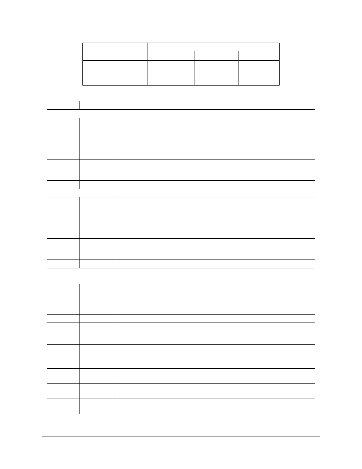
FDS 6531/6532 005 Data Sheet 71M6531D/F-71M6532D/F
Bit
Symbol
Function
Timer/Counter 1:
Timer/Counter 0:
Table 21: Allowed Timer/Counter Mode Combinations
Timer 1
Timer 0 - mode 0
Timer 0 - mode 1
Timer 0 - mode 2
Mode 0 Mode 1 Mode 2
Yes Yes Yes
Yes Yes Yes
Not allowed Not allowed Yes
Table 22: TMOD Register Bit Descriptio n (SFR 0x89)
If TMOD[7] is set, external input signal control is enabled for Counter 0.
external gate control. The TR1 bit in the TCON register (SFR 0x88) must
TMOD[7] Gate
also be set in order for Counter 1 to increment.
With these settings Counter 1 is incremented on every falling edge of the
logic signal applied to one or more of the interrupt sources controlled by
the DI_RBP, DIO_R1, … DIO_RXX registers.
Selects timer or counter operation. When set to 1, a counter operation is
TMOD[6] C/T
performed. When cleared to 0, the corresponding register will function as a
timer.
TMOD[5:4] M1:M0
Selects the mode for Timer/Counter 1 as shown in Table 20.
If TMOD[3] is set, external input signal control is enabled for Counter 0.
external gate control. The TR0 bit in the TCON register (SFR 0x88) must
TMOD[3] Gate
also be set in order for Counter 0 to increment.
With these settings Counter 0 is incremented on every falling edge of the
logic signal applied to one or more of the interrupt sources controlled by
the DI_RBP, DIO_R1, … DIO_RXX registers.
Selects timer or counter operation. When set to 1, a counter operation is
TMOD[2] C/T
performed. When cleared to 0, the corresponding re gister will funct ion as
a timer.
TMOD[1:0] M1:M0
Selects the mode for Timer/Counter 0, as shown in Table 20.
Table 23: The TCON Register Bit Functions (SFR 0x88)
Bit Symbol Function
The Timer 1 overflow flag is set by hardware when Timer 1 overflows.
TCON[7] TF1
This flag can be cleared by software and is automati cally cleared when an
interrupt is processed.
TCON[6] TR1
Timer 1 run control bit. If cleared, Timer 1 stops.
Timer 0 overflow flag set by hardware when Timer 0 overflows. This flag
TCON[5] TF0
can be cleared by software and is automatically cleared when an interrupt
is processed.
TCON[4] TR0
TCON[3] IE1
TCON[2] IT1
TCON[1] IE0
TCON[0] IT0
Timer 0 Run control bit. If cleared, Timer 0 stops.
Interrupt 1 edge flag is set by hardware when the falling edge on external
pin int1 is observed. Cleared when an interrupt i s processed.
Interrupt 1 type control bit. Selects either the f al l ing edge or low level on
input pin to cause an interrupt.
Interrupt 0 edge flag is set by hardware whe n the falling edge on external
pin int0 is observed. Cleared when an interrupt i s processed.
Interrupt 0 type control bit. Selects either the f al l ing edge or low level on
input pin to cause interrupt.
v1.3 © 2005-2010 TERIDIAN Semiconductor Corporation 29
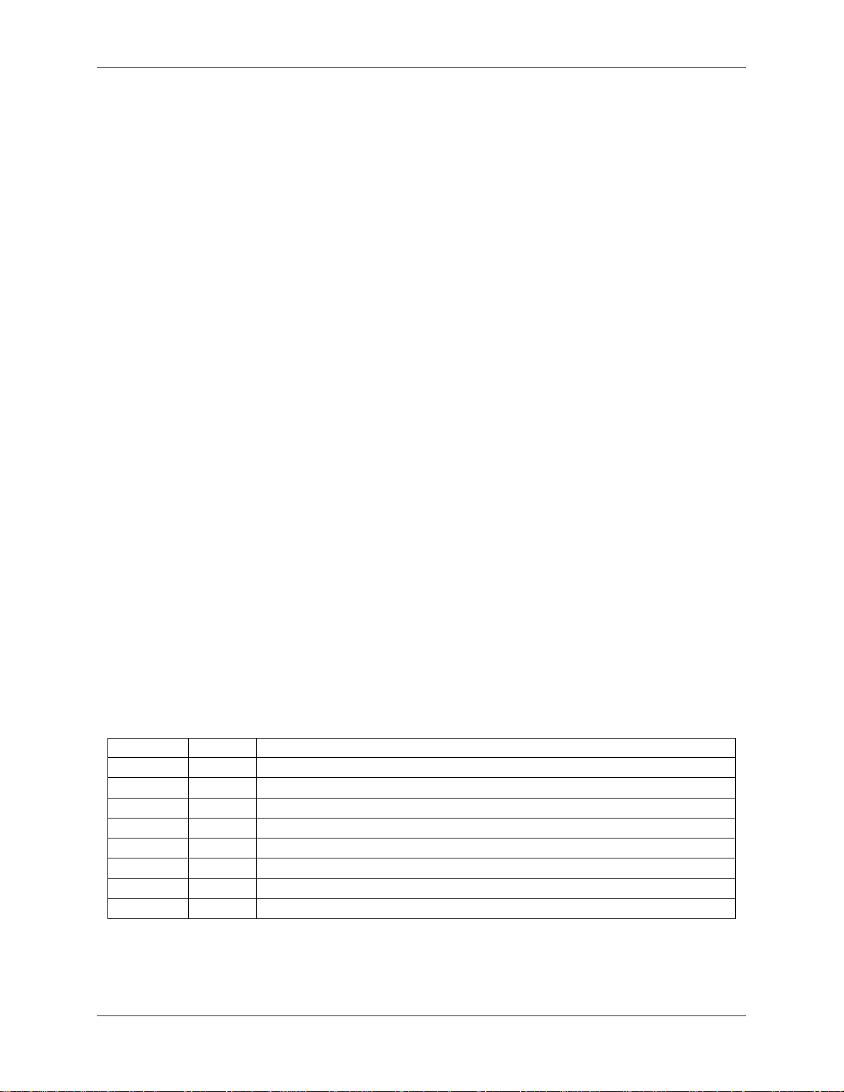
Data Sheet 71M6531D/F-71M6532D/F FDS 6531/6532 005
Bit
Symbol
Function
IEN0[7]
EAL
EAL
1.4.8 WD Timer (Software Watchdog Timer)
There is no internal software watchdog timer. Us e the standard watchdog timer instead (see 1.5.16
Hardware Watchdog Timer).
1.4.9 Interrupts
The 80515 MPU provides 11 interrupt sources with four priority l evels. Each source has its own request
flag(s) located in a special function register (TCON, IRCON and SCON). Each interrupt requested by the
corresponding flag can be individually enabled or disabled by the enable bits in SFRs IEN0 (SFR 0xA8),
IEN1 (SFR 0xB8), and IEN2 (SFR 0x9A). Figure 8 shows the device interrupt structure.
Referring to Figure 8, interrupt sources can originate from within the 80515 MPU core (referred to as
Internal Sources) or can originate from other part s of the 71M653x SoC (referred to as External Sources).
There are seven external interrupt sources, as s een in the leftmost part of Figure 8 , and in Table 24 and
Table 25 (i.e., EX0-EX6).
Interrupt Overview
When an interrupt occurs, the MPU will vector to t he predetermined address as shown in Table 36. Once
the interrupt service has begun, it can be interrupted only by a higher priority interrupt. The interrupt service
is terminated by a return from instruction, RETI. When an RETI is performed, the processor will return to
the instruction that would have been next when t he i nterrupt occurred.
When the interrupt condition occurs, the processor will also indicate this by setting a flag bit. This bit is
set regardless of whether the interrupt is enabl ed or disabled. Each interrupt flag is sampled once per
machine cycle, after that, samples are polled by the hardware. If the sample indicates a pending interrupt
when the interrupt is enabled, then the interrupt request flag is set. On the next instruction cycle, the interrupt
will be acknowledged by hardware forcing an LCALL to the appropriate vector address, if the following
conditions are met:
• No interrupt of equal or higher priority is already in progress.
• An instruction is currently being executed and i s not completed.
• The instruction in progress is not RETI or any write access to the registers IEN0, IEN1, IEN2, IP0 or IP1.
Special Function Registers for Interrupts
The following SFR registers control the interrupt functions:
• The interrupt enable registers: IEN0, IEN1 and IEN2 (see Table 24, Table 25 and Table 26.
• The Timer/Counter control registers, TCON and T2CON (see Table 27 and Table 28).
• The interrupt request register, IRCON (see Table 29).
• The interrupt priority registers: IP0 and IP1 (see Table 34).
Table 24: The IEN0 Bit Functions (SFR 0xA8)
= 0 disables all interrupts.
IEN0[6] WDT
IEN0[5]
IEN0[4] ES0
IEN0[3] ET1
IEN0[2] EX1
IEN0[1] ET0
IEN0[0] EX0
– Not Used.
Not used for interrupt control.
ES0 = 0 disables serial channel 0 interrupt.
ET1 = 0 disables timer 1 overflow interrupt.
EX1 = 0 disables external interrupt 1.
ET0 = 0 disables timer 0 overflow interrupt.
EX0 = 0 disables external interrupt 0.
30 © 2005-2010 TERIDIAN Semiconductor Corporation v1.3
 Loading...