

TERIDIAN Semiconductor 71M6531 User Manual
71M6531 Demo Board User’s Manual
71M6531 Demo Board
USER’S MANUAL
6/2/2008 5:23:00 PM
v1.5
TERIDIAN Semiconductor Corporation
6440 Oak Canyon Rd., Suite 100
Irvine, CA 92618-5201
Phone: (714) 508-8800 ▪ Fax: (714) 508-8878
http://www.teridian.com/
meter.support@teridian.com
© 2007-2008 TERIDIAN Semiconductor Corporation Page: 1 of 83
v1.5

71M6531 Demo Board User’s Manual
Page: 2 of 83 © 2007-2008 TERIDIAN Semiconductor Corporation v1.5

71M6531 Demo Board User’s Manual
TERIDIAN Semiconductor Corporation makes no warranty for the use of its products, other than expressly contained in the
Company’s warranty detailed in the TERIDIAN Semiconductor Corporation standard Terms and Conditions. The company assumes
no responsibility for any errors which may appear in this document, reserves the right to change devices or specifications detailed
herein at any time without notice and does not make any commitment to update the information contained herein.
© 2007-2008 TERIDIAN Semiconductor Corporation Page: 3 of 83
v1.5

71M6531 Demo Board User’s Manual
71M6531
Single-Phase Energy Meter IC
DEMO BOARD
USER’S MANUAL
Page: 4 of 83 © 2007-2008 TERIDIAN Semiconductor Corporation v1.5

71M6531 Demo Board User’s Manual
Table of Contents
1 GETTING STARTED........................................................................................................................................... 9
1.1 General ............................................................................................................................................................... 9
1.2 Safety and ESD Notes ....................................................................................................................................... 9
1.3 Demo Kit Contents ............................................................................................................................................ 9
1.4 Compatibility .................................................................................................................................................... 10
1.5 Suggested Equipment not Included .............................................................................................................. 10
1.6 Demo Board Test Setup .................................................................................................................................. 10
1.6.1 Power Supply Setup ................................................................................................................................... 12
1.6.2 CABLE for Serial Connection ..................................................................................................................... 13
1.6.3 Checking Operation .................................................................................................................................... 13
1.6.4 Serial Connection Setup for the PC............................................................................................................ 14
1.7 Using the Demo Board .................................................................................................................................... 15
1.7.1 Cycling the LCD Display ............................................................................................................................. 15
1.7.2 Serial Command Line Interface (CLI) ......................................................................................................... 16
1.7.3 Communicating via Intel Hex Records ....................................................................................................... 22
1.7.4 Using the Battery Modes ............................................................................................................................ 24
1.8 Using the Demo Board for Metering Functions ............................................................................................ 25
1.8.1 Modifying Demo Code to CT or SHUNT Mode ........................................................................................... 25
1.8.2 Using the Demo Board in SHUNT and CT Modes ..................................................................................... 25
1.8.3 Adjusting the kh Factor for the Demo Board .............................................................................................. 26
1.8.4 Adjusting the Demo Boards to Different CT Winding Ratios ...................................................................... 27
1.8.5 Adjusting the Demo Boards to Voltage Transformers or Different Voltage Dividers ................................... 27
1.8.6 Wiring of the Demo Board and a Shunt Resistor ........................................................................................ 27
1.9 Calibration Parameters ................................................................................................................................... 30
1.9.1 General Calibration Procedure ................................................................................................................... 30
1.9.2 Updating the 6531_demo.hex file ............................................................................................................... 30
1.9.3 Calibration Macro File ................................................................................................................................ 31
1.9.4 Updating Calibration Data in EEPROM or Flash ........................................................................................ 31
1.9.5 Loading the 6531_demo.hex file into the Demo Board............................................................................... 31
1.9.6 The Programming Interface of the 71M6531 .............................................................................................. 33
1.10 Demo Code ...................................................................................................................................................... 34
1.10.1 Demo Code Description ............................................................................................................................. 34
1.10.2 Accessing LCD and Sleep Modes from Brownout Mode ............................................................................ 34
1.10.3 Demo Code Memory Locations .................................................................................................................. 34
1.11 Emulator Operation ......................................................................................................................................... 41
2 APPLICATION INFORMATION ........................................................................................................................ 43
2.1 Calibration Theory ........................................................................................................................................... 43
2.1.1 Calibration with Three Measurements ........................................................................................................ 43
2.1.2 Calibration with Five Measurements .......................................................................................................... 45
2.1.3 Fast Calibration .......................................................................................................................................... 46
2.2 Calibration Procedures ................................................................................................................................... 47
2.2.1 General Precautions ................................................................................................................................... 47
2.2.2 Calibration Procedure with Three Measurements ...................................................................................... 48
2.2.3 Calibration Procedure with Five Measurements ......................................................................................... 48
2.2.4 Procedure for Auto-Calibration ................................................................................................................... 49
2.2.5 Calibration Spreadsheets ........................................................................................................................... 49
© 2007-2008 TERIDIAN Semiconductor Corporation Page: 5 of 83
v1.5

71M6531 Demo Board User’s Manual
2.2.6 Compensating for Non-Linearities .............................................................................................................. 51
2.2.7 Calibrating Meters with Combined CT and Shunt Resistor ........................................................................ 51
2.3 Calibrating and Compensating the RTC ........................................................................................................ 54
2.4 Testing the Demo Board ................................................................................................................................. 55
2.4.1 Functional Meter Test ................................................................................................................................. 55
2.4.2 EEPROM .................................................................................................................................................... 56
2.4.3 RTC ............................................................................................................................................................ 57
2.4.4 Hardware Watchdog Timer ........................................................................................................................ 57
2.4.5 LCD ............................................................................................................................................................ 57
2.4.6 Supply Current Measurements ................................................................................................................... 58
2.5 TERIDIAN Application Notes .......................................................................................................................... 58
3 HARDWARE DESCRIPTION ............................................................................................................................ 59
3.1 Demo Board Description: Jumpers, Switches, Test Points and Connectors ............................................ 59
3.2 Demo Board Hardware Specifications ........................................................................................................... 63
4 APPENDIX ........................................................................................................................................................ 65
4.1 71M6531N12A2 Demo Board Electrical Schematic ...................................................................................... 66
4.2 71M6531N12A2 Demo Board Bill of Material ................................................................................................. 69
4.3 71M6531N12A2 Demo Board PCB Layout ..................................................................................................... 70
4.4 Debug Board Bill of Material .......................................................................................................................... 75
4.5 Debug Board Schematics ............................................................................................................................... 76
4.6 Debug Board PCB Layout ............................................................................................................................... 77
4.7 TERIDIAN 71M6531 Pin-Out Information ....................................................................................................... 80
4.8 Revision History .............................................................................................................................................. 83
List of Figures
Figure 1-1: Demo Board: Basic Connections ............................................................................................................... 10
Figure 1-2: Demo Board: Ribbon Cable Connections .................................................................................................. 11
Figure 1-3: The TERIDIAN 6531 Demo Board with Debug Board Block Diagram (CT Configuration) ......................... 12
Figure 1-4: Port Configuration Setup ............................................................................................................................ 14
Figure 1-5: Hyperterminal Sample Window with Disconnect Button ............................................................................ 15
Figure 1-6: Pre-wired shunt resistor ............................................................................................................................. 28
Figure 1-7: Connection of the Pre-Wired Shunt Resistor ............................................................................................. 29
Figure 1-8: Typical Calibration Macro file ..................................................................................................................... 31
Figure 1-9: Emulator Window Showing Reset and Erase Buttons ............................................................................... 32
Figure 1-10: Emulator Window Showing Erased Flash Memory and File Load Menu .................................................. 32
Figure 2-1: Watt Meter with Gain and Phase Errors. ................................................................................................... 43
Figure 2-2: Phase Angle Definitions ............................................................................................................................. 47
Figure 2-3: Calibration Spreadsheet for Three Measurements .................................................................................... 49
Figure 2-4: Calibration Spreadsheet for Five Measurements ....................................................................................... 50
Figure 2-5: Calibration Spreadsheet for Fast Calibration ............................................................................................. 50
Figure 2-6: Non-Linearity Caused by Quantification Noise .......................................................................................... 51
Figure 2-7: 71M6531 with Shunt and CT ..................................................................................................................... 52
Figure 2-17: Meter with Calibration System ................................................................................................................. 56
Figure 2-18: Calibration System Screen ...................................................................................................................... 56
Figure 3-1: 71M6531N12A2 Board Connectors, Jumpers, Switches, and Test Points ................................................ 62
Figure 4-1: 71M6531N12A2 Demo Board (REV 2.0): Electrical Schematic 1/3 – Shunt Configuration ....................... 66
Figure 4-2: 71M6531N12A2 Demo Board (REV 2.0): Electrical Schematic 2/3 – CT Configuration ............................ 67
Figure 4-3: 71M6531N12A2 Demo Board (REV 2.0): Electrical Schematic 3/3 – Digital Section ................................ 68
Figure 4-4: 71M6531N12A2 Demo Board: Top Silk Screen ......................................................................................... 70
Page: 6 of 83 © 2007-2008 TERIDIAN Semiconductor Corporation v1.5

71M6531 Demo Board User’s Manual
Figure 4-5: 71M6531N12A2 Demo Board: Top Copper Layer ..................................................................................... 71
Figure 4-6: 71M6531N12A2 Demo Board: Bottom View with Silk Screen ................................................................... 72
Figure 4-7: 71M6531N12A2 Demo Board: Bottom Copper Layer – Bottom View ........................................................ 73
Figure 4-8: 71M6531N12A2 Demo Board: Bottom Copper Layer – Layer View from Top ........................................... 74
Figure 4-9: Debug Board: Electrical Schematic ........................................................................................................... 76
Figure 4-10: Debug Board: Top View ........................................................................................................................... 77
Figure 4-11: Debug Board: Bottom View ...................................................................................................................... 77
Figure 4-12: Debug Board: Top Signal Layer ............................................................................................................... 78
Figure 4-13: Debug Board: Middle Layer 1, Ground Plane .......................................................................................... 78
Figure 4-14: Debug Board: Middle Layer 2, Supply Plane ........................................................................................... 79
Figure 4-15: Debug Board: Bottom Trace Layer .......................................................................................................... 79
Figure 4-16: TERIDIAN 71M6531 LQFP64: Pinout (top view) ..................................................................................... 82
List of Tables
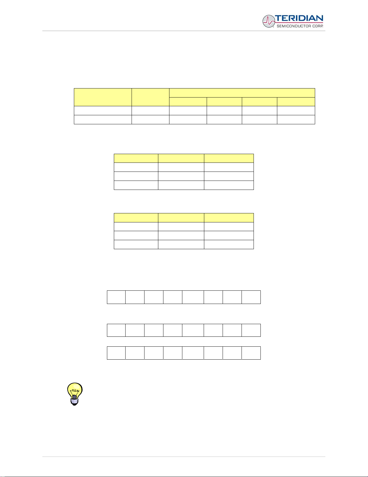
Table 1-1: Jumper settings on Debug Board ................................................................................................................ 13
Table 1-2: Straight cable connections .......................................................................................................................... 13
Table 1-3: Null-modem cable connections ................................................................................................................... 13
Table 1-4: COM Port Setup Parameters ...................................................................................................................... 14
Table 1-5: Selectable Display Options ......................................................................................................................... 16
Table 1-6: Fields of a Hex Record ................................................................................................................................ 22
Table 1-7: Data (command) types ................................................................................................................................ 23
Table 1-8: Hex Record examples ................................................................................................................................. 23
Table 1-9: Pre-assembled hex records ........................................................................................................................ 24
Table 1-10: XRAM Locations for Calibration Constants ............................................................................................... 30
Table 1-11: Flash Programming Interface Signals ....................................................................................................... 33
Table 1-12: MPU memory locations ............................................................................................................................. 38
Table 1-13: Values for Pulse Source Registers............................................................................................................ 39
Table 1-14: STATUS register ......................................................................................................................................... 40
Table 1-15: MPU Accumulation Output Variables ........................................................................................................ 41
Table 2-1: Calibration Summary ................................................................................................................................... 54
Table 3-1: 71M6531 Demo Board description: 1/3 ....................................................................................................... 59
Table 3-2: 71M6531 Demo Board description: 2/3 ....................................................................................................... 60
Table 3-3: 71M6531 Demo Board description: 3/3 ....................................................................................................... 61
Table 4-1: 71M6531N12A2 Demo Board: Bill of Material (Shunt Version) ................................................................... 69
Table 4-2: Debug Board: Bill of Material ...................................................................................................................... 75
Table 4-3: 71M6531 Pin description 1/2 ....................................................................................................................... 80
Table 4-4: 71M6531 Pin description 2/2 ....................................................................................................................... 82
© 2007-2008 TERIDIAN Semiconductor Corporation Page: 7 of 83
v1.5

71M6531 Demo Board User’s Manual
Page: 8 of 83 © 2007-2008 TERIDIAN Semiconductor Corporation v1.5

71M6531 Demo Board User’s Manual
1
1 GETTING STARTED
1.1 GENERAL
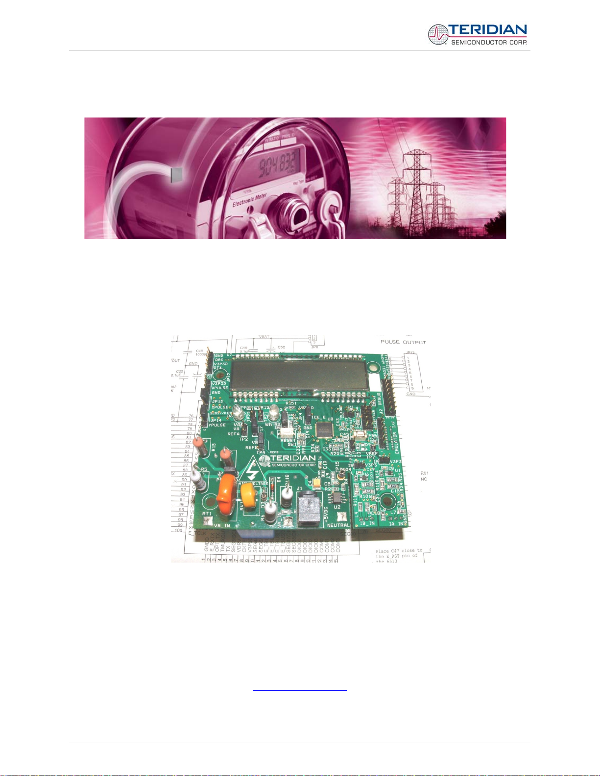
The TERIDIAN Semiconductor Corporation (TSC) 71M6531 Demo Board is an energy meter IC demonstration board for evaluating the 71M6531D/F device for residential electronic energy metering applications. It
incorporates a 71M6531D/F integrated circuit, peripheral circuitry such as a serial EEPROM, emulator port,
and on-board power supply as well as a companion Debug Board that allows a connection to a PC through
a RS232 port. The Demo Board allows the evaluation of the 71M6531D/F energy meter controller chip for
measurement accuracy and overall system use.
The board is pre-programmed with a Demo Program (file name 6531_demo.hex) in the FLASH memory of
the 71M6531D/F IC. This embedded application is developed to exercise all low-level functions to directly
manage the peripherals and CPU (clock, timing, power savings, etc.).
1.2 SAFETY AND ESD NOTES
Connecting live voltages to the Demo Board system will result in potentially hazardous voltages on the
Demo Board.
EXTREME CAUTION SHOULD BE TAKEN WHEN HAN DLING THE DEMO BOARD
ONCE IT IS CONNECTED TO LIVE VOLTAGES!
THE DEMO SYSTEM IS ESD SENSITIVE! ESD PRECAUTIONS SHOULD BE
TAKEN WHEN HANDLING THE DEMO BOARD!
1.3 DEMO KIT CONTENTS
• 71M6531 Demo Board containing 71M6531D/F IC with preloaded Demo Program and prepared for
either CT or shunt resistor operation
• Debug Board
• Shunt resistor with wire harness, 400µΩ (for kits shipped in shunt configuration)
• Two 5VDC/1,000mA universal wall transformers w/ 2.5mm plug (Switchcraft 712A)
• Serial cable, DB9, Male/Female, 2m length (Digi-Key AE1379-ND)
• CD-ROM containing documentation (data sheet, board schematics, BOM, layout), Demo Code, and
utilities
v1.5
Note: The CD-ROM contains a file named readme.txt that specifies all files found on the media and their
purpose.
© 2007-2008 TERIDIAN Semiconductor Corporation
Page: 9 of 83
71M6531 Demo Board User’s Manual
1.4 COMPATIBILITY
This manual applies to the following hardware and software revisions:
• 71M6531D/F, chip revision A03
• Demo Boards D6531N12A2
• Demo Board Code revision 6531_4p6q_12may08_0cc.hex, 6531_4p6q_12may08_0sc.hex (EQU 0) ,
6531_4p6q_12may08_1cc.hex EQU 1), 6531_4p6q_12may08_2cc.hex (EQU 2), or later
1.5 SUGGESTED EQUIPMENT NOT INCLUDED
For functional demonstration:
®
• PC w/ MS-Windows
connector
• One or two current transformers (CTs), preferably 2,000:1 turns ratio
• For software development (MPU code):
• Signum ICE (In Circuit Emulator): ADM-51
• http://www.signum.com
• Keil 8051 “C” Compiler kit: CA51
versions XP, ME, or 2000, equipped with RS232 port (COM port) via DB9
http://www.keil.com/c51/ca51kit.htm
, http://www.keil.com/product/sales.htm
1.6 DEMO BOARD TEST SETUP
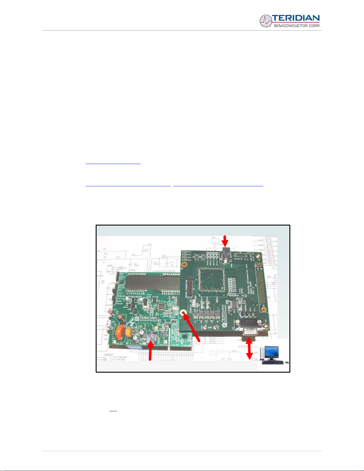
Figure 1-1 shows the basic connections of the Demo Boards plus Debug Boards with the external
equipment.
Demo
Board
5VDC Power
Debug
Board
Spacer
removed
5VDC Power
Figure 1-1: Demo Board: Basic Connections
The Debug Board can be plugged into J2 of the Demo Board. One spacer of the Debug Board should be
removed, as shown in Figure 1-1. Alternatively, both boards can be connected using a flat ribbon cable, as
shown in Figure 1-2. A male header has to be soldered to J3 of the Debug Board, and the female-to-female
flat ribbon cable is not
Page: 10 of 83 © 2007-2008 TERIDIAN Semiconductor Corporation v1.5
supplied with the Demo Kit (use Digi-Key P/N A3AKA-1606M-ND or similar).
Host PC
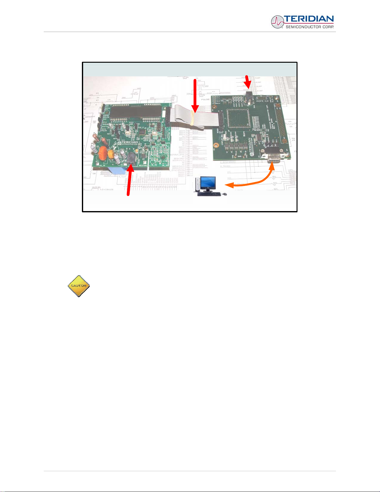
71M6531 Demo Board User’s Manual
Ribbon Cable
5VDC Power
Demo
Debug Board
Board
5VDC Power
Figure 1-2: Demo Board: Ribbon Cable Connections
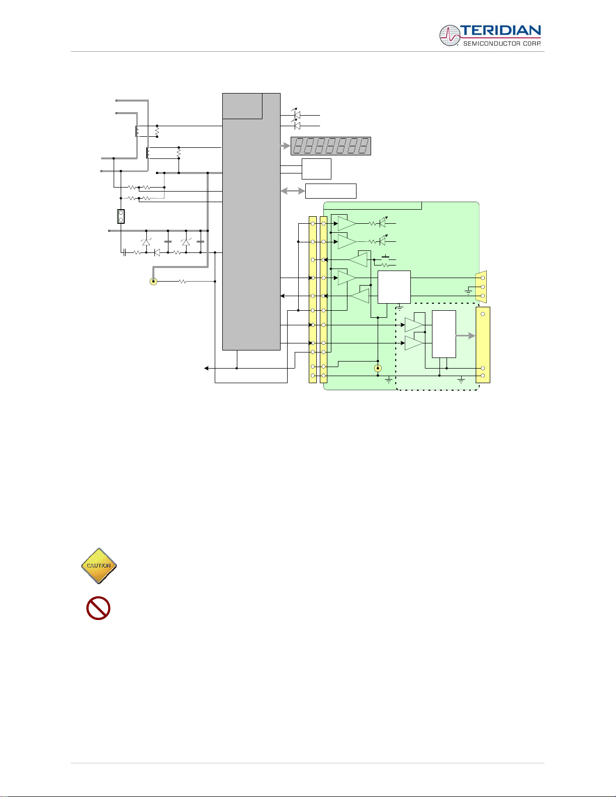
The 71M6531 Demo Board block diagram is shown in Figure 1-3. It consists of a stand-alone meter Demo
Board and an optional Debug Board. The Demo Board contains all circuits necessary for operation as a
meter, including display, calibration LED, and power supply. The Debug Board, when not sharing a power
supply with the meter, is optically isolated from the meter and interfaces to a PC through a 9 pin serial port.
Connections to the external signals to be measured, i.e. scaled AC voltages and current signals derived
from shunt resistors or current transformers, are provided on the rear side of the Demo Board.
It is recommended to set up the Demo Board with no live AC voltage connected, and to
connect live AC voltages only after the user is familiar with the demo system.
Host PC
v1.5
© 2007-2008 TERIDIAN Semiconductor Corporation
Page: 11 of 83
71M6531 Demo Board User’s Manual
DEMONSTRATION METER
LOAD A
LOAD B
VB
VA
NEUTRAL
6531
Single Chip
Meter
IB
External Current
Transformers
IA
IB
IA
V3P3
DIO6
DIO7
DIO4
DIO5
VB
VA
JP1
V3P3
3.3V
GND
GND
5V DC
TMUXOUT
CKTEST
V3P3D
On-board
components
powered by V3P3D
TX
RX
Wh
VARh
3.3V LCD DISPLAY
EEPROM
ICE Connector
1
2
3
N/C
10
12
5, 7,
GND
9, 11
8
6
4
15, 16
N/C
13, 14
N/C
J2
V3P3
V3P3
DEBUG BOARD (OPTIONAL)
ISO
ISO
ISO
ISO
6
V5_DBG
RS-232
INTERFACE
ISO
5V DC
GND_DBG
JP21
MPU HEARTBEAT (5Hz)
V5_DBG
CE HEARTBEAT (1Hz)
V5_DBG
GND_DBG
V5_DBG
RTM INTERFACE
FPGA
ISO
ISO
V5_NI
DB9
to PC
COM Port
4/12/2007
DB9
to PC
COM Port
Figure 1-3: The TERIDIAN 6531 Demo Board with Debug Board Block Diagram (CT Configuration)
Note: All analog input signals are referenced to the V3P3A net (3.3V power supply to the chip).
1.6.1 POWER SUPPLY SETUP
There are several choices for meter the power supply:
• Internal (using the AC line voltage). The internal power supply is only suitable when the line voltage
exceeds 220V RMS.
• External 5VDC connector (J1) on the Demo Board
• External 5VDC connector (J1) on the Debug Board.
The power supply jumper, JP1, must be consistent with the power supply choice. JP1 connects the AC
line voltage to the internal power supply. This jumper should usually be left in place.
When the Demo Board is in shunt configuration, the shunt resistor has to be connected as shown in
Figure 1-7 for the board to be powered via J1. Alternatively, a jumper cable between any header labeled
V3P3 and the NEUTRAL terminal (J9) can be supplied.
Page: 12 of 83
© 2007-2008 TERIDIAN Semiconductor Corporation
v1.5
71M6531 Demo Board User’s Manual
1.6.2 CABLE FOR SERIAL CONNECTION
For connection of the DB9 serial port to a PC, either a straight or a so-called “null-modem” cable may be
used. JP1 and JP2 are plugged in for the straight cable, and JP3/JP4 are empty. The jumper configuration is
reversed for the null-modem cable, as shown in Table 1-3.
Cable
Configuration
Straight Cable
Null-Modem Cable Alternative -- -- Installed Installed
JP1 through JP4 can also be used to alter the connection when the PC is not configured as a DCE device.
Table 1-2 shows the connections necessary for the straight DB9 cable and the pin definitions.
Table 1-3 shows the connections necessary for the null-modem DB9 cable and the pin definitions.
Mode
Default
Table 1-1: Jumper settings on Debug Board
PC Pin Function Demo Board Pin
2 TX 2
3 RX 3
5 Signal Ground 5
Table 1-2: Straight cable connections
PC Pin Function Demo Board Pin
2 TX 3
3 RX 2
5 Signal Ground 5
Table 1-3: Null-modem cable connections
JP1 JP2 JP3 JP4
Installed Installed -- --
Jumpers on Debug Board
1.6.3 CHECKING OPERATION
A few seconds after power up, the LCD display on the Demo Board should briefly display the following
welcome text:
H E L L 0
After the “HELLO” text, the LCD should display the following information:
W h
and:
0. 0 0 1
The text “Wh” indicates that accumulated Watt-hours are displayed. In the case shown above, 0.001 Wh
were accumulated. The display will be cycling from numeric to text, indicating activity of the MPU inside the
D/F. 71M6531
In Mission Mode, the display can be cycled to display VARh, PF and other parameters by pressing
the pushbutton (PB).
© 2007-2008 TERIDIAN Semiconductor Corporation Page: 13 of 83
v1.5
71M6531 Demo Board User’s Manual
r
V
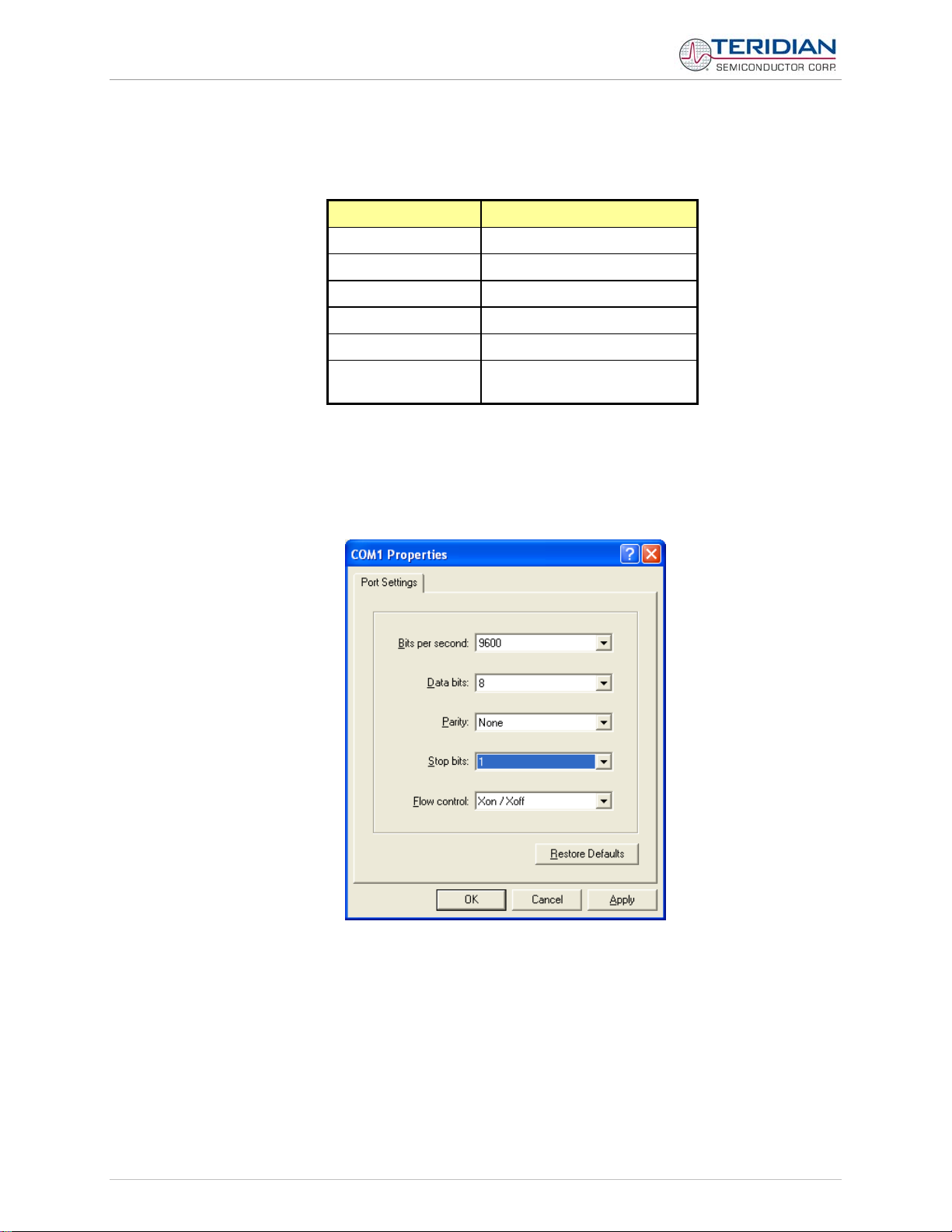
1.6.4 SERIAL CONNECTION SETUP FOR THE PC
After connecting the DB9 serial port to a PC, start the HyperTerminal application (or any other suitable
communication program) and create a session using the communication parameters shown in Table 1-4.
Setup Paramete
Port speed (baud) 9600/300g
Data bits 8
Parity none
Stop bits 1
Flow control XON/XOFF
Table 1-4: COM Port Setup Parameters
HyperTerminal can be found by selecting Programs ÆAccessories Æ Communications from the Windows
start menu. The connection parameters are configured by selecting File Æ Properties and then by pressing
the Configure button (see Figure 1-4).
A setup file (file name “Demo Board Connection.ht”) for HyperTerminal that can be loaded with File Æ Open
is also provided with the tools and utilities on the supplied CD-ROM.
g depending on the jumper
alue
setting at JP12
©
Figure 1-4: Port Configuration Setup
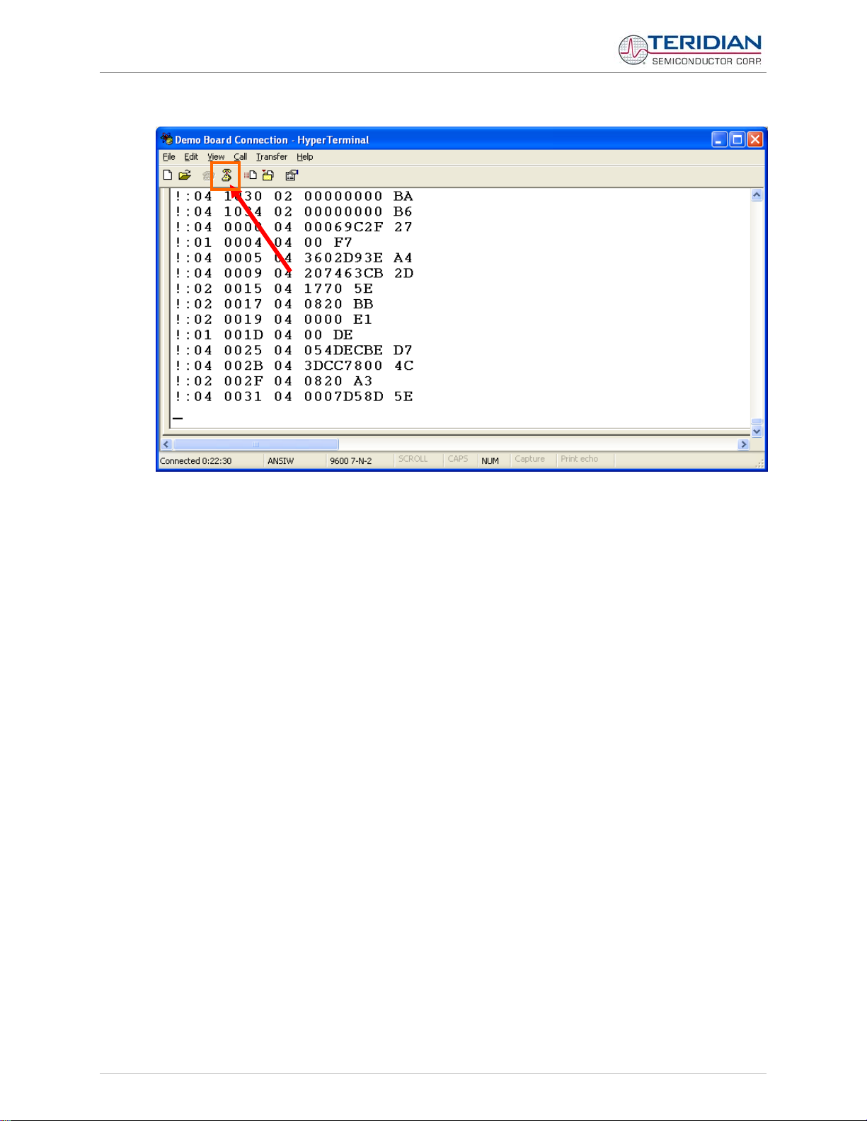
Note: Port parameters can only be adjusted when the connection is not active. The disconnect button, as
shown in Figure 1-5 must be clicked in order to disconnect the port.
Page: 14 of 83 © 2007-2008 TERIDIAN Semiconductor Corporation v1.5
71M6531 Demo Board User’s Manual
Figure 1-5: Hyperterminal Sample Window with Disconnect Button
1.7 USING THE DEMO BOARD
The 71M6531 Demo Board is a ready-to-use meter prepared for use with an external shunt resistor.
Using the Demo Board involves communicating with the Demo Code. An interactive command line interface
(CLI) is available as part of the Demo Code. The CLI allows modifications to the metering parameters,
access to the EEPROM, initiation of auto-calibration sequences, selection of the displayed parameters,
changing calibration factors and many more operations.
Before evaluating the 71M6531 Demo Board, users should get familiar with the commands and responses
of the CLI. A complete description of the CLI is provided in section 1.7.2.
1.7.1 CYCLING THE LCD DISPLAY
The Demo Codes for the 71M6531 Demo Board allow cycling of the display using the PB button. By briefly
pressing the button, the next available parameter from Table 1-5 is selected. This makes it easy to navigate
various displays for Demo Boards that do not have the CLI.
© 2007-2008 TERIDIAN Semiconductor Corporation Page: 15 of 83
v1.5
71M6531 Demo Board User’s Manual
r
Step Text Display Displa yed Paramete
1
2
3
4
5
6
7
8
8
8
8
8
Pulses
Bat V
Delta T
Wh
VARh
Hours
Time
Date
PF
Edges
A
V
Accumulated real energy [Wh]. The default display setting after power-up
or reset.
Accumulated reactive energy [VARh].
Expired hours after power-up or reset
Time of day (hh.mm.ss).
Date (yyyy.mm.dd).
Current power factor.
Count of zero crossings in the last accumulation interval.
Number of emitted pulses.
RMS current at phase A input [A].
RMS voltage at the VA_IN input [V].
Measured battery voltage [V].
Temperature difference from calibration temperature. Displayed in 0.1°C
Table 1-5: Selectable Display Options
1.7.2 SERIAL COMMAND LINE INTERFACE (CLI)
Once, communication to the Demo Board is established, press <CR> and the Demo Program prompt (“>”)
should appear. Type >i to verify that the Demo Program version is revision 4p6q or later.
Users should familiarize themselves with the Demo Program commands described in the tables below.
The Demo Program (Demo Code) is compiled with EEPROM specified as the non-volatile memory. This
means that the default calibration factors are stored in flash memory while the calibration factors resulting
from an actual calibration are stored in EEPROM.
The tables below describe the commands in detail. Type ‘?’ for a display of available commands.
Page: 16 of 83 © 2007-2008 TERIDIAN Semiconductor Corporation v1.5
71M6531 Demo Board User’s Manual
Commands for CE Data Access:
] CE DATA ACCESS Remarks
Description: Allows user to read from and write to CE data space.
Usage: ] [Starting CE Data Address] [option]…[option]
Command
]??? Read consecutive 16-bit words in Decimal
combinations:
]$$$ Read consecutive 16-bit words in Hex
Update .
]U
default version of CE Data in EEPROM
Important: The CE must be stopped (C
E0)
before issuing this command!
Example: ]40$$$ Reads s 0x40, 0x41 and 0x42. CE data word
]7E=12345678=9876ABCD Writes two words starting @ 0x7E
CE da from rds are in 4-byte (32-
ta space is the address range 0x1000 to 0x13FF. All CE data wo
bit) format. The offset of 0x1000 does not have to be entered when using the ] command, thus
typing ]A? will access the 32-bit word located at the byte address 0x1000 + 4 * A = 0x1028.
Commands for MPU/XDATA Access:
) MPU DATA ACCESS Remarks
Description: and write Allows user to read from to MPU data space.
Usage: ) [Starting MPU Data Address] [option]…[option]
Command
c :
ombinations
)??? Read three consecutiv
e 32-bit words in Decimal
)$$$ Read three consecutive 32-bit words in Hex
)a=n=m
Write the values n and m to two consecutive
addresses starting at a
Example: )08$$$$ 0x0C, 0x10, 0x14 Reads data words 0x08,
)04=12345678=9876ABCD Writes two words starting @ 0x04
MPU o XDATA for th . All MPU data words r space is the address range e MPU XRAM (0x0000 to 0x0FFF)
are in 4-byte (32-bit) format. Typing ]A? will access the 32-bit word located at the byte address 4 *
A = 0x28. The energy accumulation registers of the Demo Code can be accessed by typing two
question marks (“??”).
© 2007-2008 TERIDIAN Semiconductor Corporation Page: 17 of 83
v1.5
71M6531 Demo Board User’s Manual
Commands for I/O RAM (Configuration RAM) and SFR Control:
R DIO AND SFR CONTROL Remarks
Description: Allows the user to read from and write to I/O RAM and special function registers (SFRs).
Usage: R [option] [register] … [option]
Command
combinations:
RIx…
Select I/O RAM location x (0x2000 offset is automatically added)
Rx… Select internal SFR at address x
Rx???... Read consecutive SFR registers in decimal
Rx$$$... Read consecutive registers in hex notation
Example: RI60$$$$ Read all four RTM probe registers
DIO or Configuration RAM space is the address range 0x2000 to 0x20FF. This RAM contains
registers used for configuring basic hardware and functional properties of the 71M6531D/F and is
organized in bytes (8 bits). The 0x2000 offset is automatically added when the command RI is
typed. The SFRs (special function registers) are located in internal RAM of the 80515 core,
starting at address 0x80.
Commands for EEPROM Control:
EE EEPROM CONTROL Remarks
Description: Allows user to enable read and write to EEPROM.
Usage: EE [option] [arguments]
Command
EECn EEPROM Access (1 Æ Enable, 0 Æ Disable)
combinations:
EERa.b Read EEPROM at address 'a' for 'b' bytes.
EEE Erase the EEPROM
EESabc..xyz Write characters to buffer (sets Write length)
EETa Transmit buffer to EEPROM at address 'a'.
EEWa.b...z Write values to buffer
Example: EEShello; EET$0210 Writes 'hello' starting at EEPROM address 0x210.
The EEC1 command must be issued before the EEPROM interface can be used. The execution of the EEE
command takes several seconds. During this time, no other commands can be entered.
Auxiliary Commands:
AUXILIARY Remarks
Description: Various
Commands: ,
Typing a comma (“,”) repeats the command issued
from the previous command line. This is very helpful
when examining the value at a certain address over
time, such as the XRAM address for the temperature.
/
The slash (“/”) is useful to separate comments from
commands when sending macro text files via the serial
interface. All characters in a line after the slash are
ignored.
? Displays the help menu.
CLC Enables communication via hex records.
BT Commands execution of a battery test.
Page: 18 of 83 © 2007-2008 TERIDIAN Semiconductor Corporation v1.5
71M6531 Demo Board User’s Manual
Commands controlling the CE:
C COMPUTE ENGINE
Remarks
CONTROL
Description: Allows the user to enable and configure the compute engine.
Usage: C [option] [argument]
Command
CEn Compute Engine Enable (1 Æ Enable, 0 Æ Disable)
combinations:
CTn
Select input n for TMUX output pin. Enter n in hex
notation.
CREn RTM output control (1 Æ Enable, 0 Æ Disable)
CRSa.b.c.d
Selects CE addresses for RTM output (maximum of
four)
Example: CE0 Disables the CE
CT1E Selects the CE_BUSY signal for the TMUX output pin
Calibration Commands:
CL CALIBRATION CONTROL Remarks
Description:
Calibration-related commands. A full auto-calibration can be implemented by compiling the
Demo Code with auto-calibration selected as an option. Due to space restrictions, the
auto-calibration is not implemented in the Demo Code supplied with the Demo Boards.
Usage: CL [option]
Command
CLC Loads a calibration via serial port
combinations:
CLB Starts an auto-calibration sequence
CLD Restores calibration to defaults
CLR Restores calibration from EEPROM
CLS Saves calibration to EEPROM
Commands for Identification and Information:
I INFORMATION MESSAGES Remarks
Description: Allows user to display information messages.
Usage: I
Example: I Returns the Demo Code version
The I command is used to identify the revisions of Demo Code and the contained CE code.
© 2007-2008 TERIDIAN Semiconductor Corporation Page: 19 of 83
v1.5
71M6531 Demo Board User’s Manual
Commands for Controlling the Metering Values Shown on the LCD Display:
M
Description: Allows user to select internal variables to be displayed.
Usage: M [option]. [option]
Command
combinations:
M1 Temperature (C° delta from nominal)
M2 Frequency (Hz)
M3. [phase] kWh Total Consumption (display wraps around at 999.999)
M4. [phase]
M5. [phase] kVARh Total Consumption (display wraps around at 999.999)
M6. [phase]
M7. [phase] VAh Total (display wraps around at 999.999)
M9 Real Time Clock
M10 Calendar Date
M13. n Main edge count (n = 0: accumulated, n = 1: last second)
M17 Battery voltage. Display will return to M3 after a few seconds.
Example: M3.1 Displays Wh total consumption of phase A.
Displays for total consumption wrap around at 999.999kWh (or kVARh, kVAh) due to the
number of available display digits. Internal registers (counters) of the Demo Code are 64 bits
wide and do not wrap around.
T
he internal accumulators in the Demo Code use 64 bits and will neither overflow nor wrap
a
round under normal circumstances. The restriction to only six digits is due to the
r
equirement to provide one digit showing the display mode that is separated by a blank digit
f
rom the displayed values.
METER DISPLAY
CONTROL (LCD)
M kWh Total Consumption (display wraps around at 999.999)
Remarks
kWh Total Inverse Consumption (display wraps around at
999.999)
kVAh Total Inverse Consumption (display wraps around at
999.999)
C
ommands for Controlling the RMS Values Shown on the LCD Display:
MR METER RMS DISPLAY
CONTROL (LCD)
Description: Allows user to select meter RMS display for voltage or current.
Usage: MR [option]. [option]
Command
combinations:
MR2. [phase] Displays instantaneous RMS voltage
Example: MR1.2 Displays phase b RMS current.
Commands for Controlling the MPU Power Save Mode:
PS POWER SAVE MODE Remarks
Description: Enters power save mode
Usage: PS
Return to normal mode is achieved by issuing a hardware reset.
MR1. [phase] Displays instantaneous RMS current
Remarks
Disables CE, ADC, CKOUT, ECK, RTM, TMUX VREF,
and serial port, sets MPU clock to 38.4KHz.
Page: 20 of 83 © 2007-2008 TERIDIAN Semiconductor Corporation v1.5
71M6531 Demo Board User’s Manual
Commands for Controlling the RTC:
RT REAL TIME CLOCK
Remarks
CONTROL
Description: Allows the user to read and set the real time clock.
Usage: RT [option] [value] … [value]
Command
combinations:
RTDy.m.d.w: Day of week
(year, month, day, weekday [1 = Sunday]). Weekday is
automatically set if omitted.
RTR Read Real Time Clock.
RTTh.m.s Time of day: (hr, min, sec).
RTAs.t Real Time Adjust: (speed, trim)
Example: RTD05.03.17.5 Programs the RTC to Thursday, 3/17/2005
Reset Commands:
Z, W RESET Remarks
Description: Allows the user to cause soft or watchdog resets
Usage: Z Soft reset
W Simulates watchdog reset
The Z command acts like a hardware reset. The energy accumulators in XRAM will retain their values.
Commands for Controlling the LCD and Sleep Modes (when in Brownout Mode):
B POWER MODE CONTROL Remarks
Description: Allows the user switch to LCD and Sleep mode when the 71M6531D/F is in Brownout
mode.
Usage: B [option] [value]
Command
combinations:
BL Enters LCD mode
BS Enters Sleep mode
BWSn Prepares Sleep mode with the wakeup timer set to n
seconds
BWMm Prepares Sleep mode with the wakeup timer set to m
minutes
Example: BWS8
BS
Enters Sleep mode with the wakeup timer set to 8
seconds. The 71M6531D/F will enter Sleep mode and
return to Brownout mode after 8 seconds.
© 2007-2008 TERIDIAN Semiconductor Corporation Page: 21 of 83
v1.5
71M6531 Demo Board User’s Manual
Commands for Error Recording:
ER ERROR RECORDING Remarks
Description: Allows the user display and clear the error log.
Usage: ER [option] [value]
Command
combinations:
ERD Displays error log
ERS+n Enters error number n in error log
Example: ERS+10 Enters error number 10 in error log
ERC Clears all errors from error log
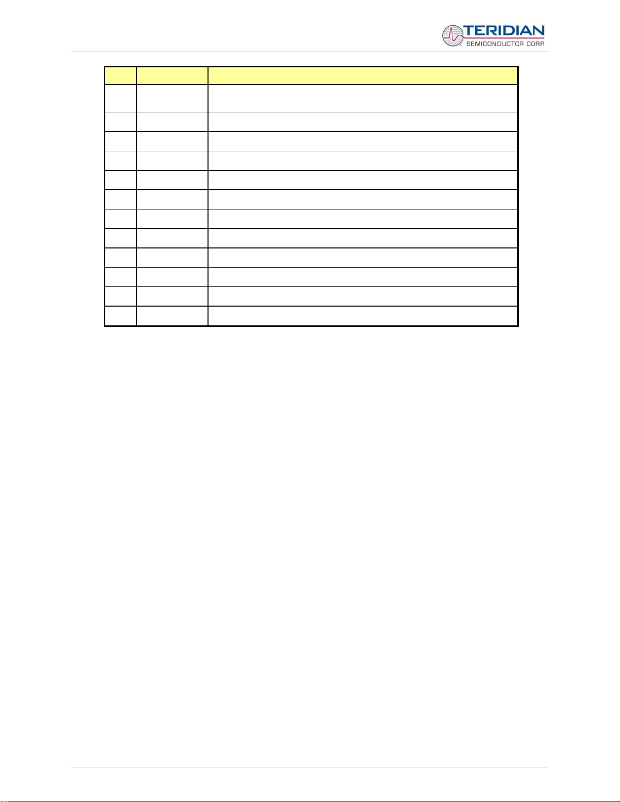
1.7.3 COMMUNICATING VIA INTEL HEX RECORDS
Communication with the 71M6531D/F IC, especially by computers and/or ATE, may also be accomplished
using a simplified protocol based on Intel Hex records. These records can still be sent and received with an
ordinary terminal, and coding and decoding of commands and responses is straight-forward.
Using the Hex-Record Format
Intel's Hex-record format allows program or data files to be encoded in a printable (ASCII) format, allowing
editing of the object file with standard tools and easy file transfer between a host and target. An individual
hex-record is a single line in a file composed of one or several Hex-records.
Entering “CLC” from the text-based command line interface enables the hex-record interface.
Hex-Records are character strings made of several fields which specify the record type, record length,
memory address, data, and checksum. Each byte of binary data is encoded as a 2-character hexadecimal
number: the first ASCII character representing the high-order 4 bits, and the second the low-order 4 bits of
the byte. The six fields that comprise a Hex-record are defined in Table 1-6.
Field Name Characters Description
1 Start code 1 An ASCII colon (":")
2 Byte count 2 The count of the character pairs in the data field.
The 2-byte address at which the data field is to be loaded into
3 Address 4
4 Type 2 00, 01, or 02.
5 Data 0-2n
6 Checksum 2
Table 1-6: Fields of a Hex Record
Each record may be terminated with a CR/LF/NULL character. Accuracy of transmission is ensured by the
byte count and checksum fields. This is important when series of values such as calibration constants are
transmitted to a meter, e.g. by ATE equipment in a factory setting. When entering hex records manually, the
user may also choose “FF” (“wild card”) as the checksum. In this case, the Demo Code omits comparing the
checksum with the received record(s).
This is how the checksum is calculated manually (if necessary):
1) The hex values of all bytes (except start code and checksum itself) are added up.
2) The last two hex digits are subtracted from 0xFF.
3) The value 0x01 is added.
memory. This is the physical XRAM or I/O RAM address, not
the 4-byte address used by the command-line interface (CLI).
From 0 to n bytes of executable code, or memory loadable
data.
n is normally 20 hex (32 decimal) or less.
The least significant byte of the two's complement sum of the
values represented by all the pairs of characters in the record
except the start code and checksum.
Page: 22 of 83 © 2007-2008 TERIDIAN Semiconductor Corporation v1.5
71M6531 Demo Board User’s Manual
As opposed to the standardized Hex-records that offer three possible types (data, termination, segment
base), six different types are supported for communicating with the 71M6531D/F. These data types basically
encode command types (read/write) along with the data source or destination, as listed in Table 1-7.
Number Code Function
1 00 Write CE data record, contains data and 16-bit CE address (CE data RAM is
located at 0x1000).
2 01 End Of File (Quit) record, a file termination record. Contains no data. This record
has to be the last line of the file, and only one record per file is permitted. The
byte pattern is always ':00000001FF'.
Upon receipt of this record, the Demo Code will transfer the received data into
non-volatile memory (EEPROM).
3 02 Alternate form of Write CE data record (optional). CE data RAM is located at
0x1000.
4 03 Read CE data record, contains empty data field and 16-bit CE address (optional).
CE data RAM is located at 0x1000.
5 04 Write MPU or I/O RAM data record, contains data and 16-bit MPU address.
6 05 Read MPU or I/O RAM data record, contains empty data field and 16-bit MPU
address (optional). I/O RAM is located at 0x2000.
7 06 Write RTC data record, contains data and 16-bit RTC address.
8 07 Read RTC data record, contains empty data field and 16-bit RTC address
(optional).
9 08 Write SFR data record, contains data and 16-bit SFR address (optional). The
MSB is always zero (0).
10 09 Read SFR data record, contains empty data field and 16-bit SFR address
(optional).
Table 1-7: Data (command) types
Table 1-8 lists a few examples of hex records.
Hex Record Function
:08 0000 06 00 00 0C 03 18 05 06 00 ff
Writes (06) eight bytes (08) to RTC, setting the
RTC to zero seconds (00), minutes (00), 12
hours (0C), Wednesday (03), 24
(05), 2006 (06). Uses the wild card checksum.
:10 0010 00 00004000 00004000 00004000
00004000 E8
:00 0000 01 FF
Writes the default values (0x4000) for the
calibration constants CAL_IA, CAL_IB,
CAL_VA, and CAL_VC to the XRAM (00),
starting at address 0x10 (0010).
The second command causes the Demo Code
to write the data to permanent storage.
:10 1020 03 FF
Causes the Demo Board to display the CE data
from address 0x1020 to 0x102F
Table 1-8: Hex Record examples
The Demo Board will not echo any inputs from the terminal (they screen will stay blank except for
the asterisk (*) issued after the user enters <CR><LF>). It is useful to configure Hyperterminal for
“auto-echo”. This can be done by selecting “Properties” from the “File” menu, then clicking on the
“Settings” tab and clicking the “ASCII Setup” button.
No <ENTER> key is necessary at the end of a manually entered record.
th
(18) of May
© 2007-2008 TERIDIAN Semiconductor Corporation Page: 23 of 83
v1.5
71M6531 Demo Board User’s Manual
Spaces in between the fields (to increase readability), as in the example above, are ignored by the Demo
Boards.
If a hex record is accepted, the Demo Board returns a "
Board sends a "
When only a partial record is entered, the Demo Board will time out after around 30 seconds and then send
<CR>< LF>.
A number of pre-assembled hex records is supplied with the Demo Code. It is easier to send a pre-assembled record using the “send text file” feature in the “Transfer” menu of Hyperterminal, than assembling hex
record from scratch.
The pre-assembled hex records are contained in a ZIP file named 6531_scripts.zip on the CD-ROM
supplied with the Demo Kits. Table 1-9 shows the records available and their function.
Hex Record Name Function
set_6531_defaults.txt
read_6531_temp.txt
set_6531_temp.txt
read_6531_power.txt
read_6531_ce.txt
read_6531_config.txt
set_6531_rtm.txt
?" and other text, depending on the context (only the 16KB Demo Code will send text).
Sets the default configuration, including all CE variables. Transferring
this record is necessary when data in the EEPROM is lost or
compromised.
Displays the current temperature reading from the CE
This record can be edited to set the nominal (calibration) temperature
Displays the valid power data
Displays CE data from memory locations 0x1020 to 0x10FF
Displays configuration data. This hex record includes comment text
helping to interpret the received data.
Sets up the real-time monitor
!". If the hex record is not accepted, the Demo
Table 1-9: Pre-assembled hex records
1.7.4 USING THE BATTERY MODES
The 71M6531D/F is in so-called Mission mode, as long as 3.3VDC is supplied to the V3P3SYS pin. If this
voltage is below the minimum required operating voltage which is usually indicated by V1 < 1.6 (internal
VBIAS voltage), and if no battery is connected to the VBAT pin, the chip is powered off.
Battery modes can be used if a battery or other DC source supplying a DC voltage with in the operating
limits for the battery input is applied to the battery pin (VBAT, pin 49) of the chip. On the Demo Board, the
battery should be connected to pin 2 (+) and 3 (-) of JP8.
In order to prevent corruption of external memory, which could occur when main power
is removed from the Demo Board while no batter y is present, the Demo Cod e is shipped
with the battery modes DISABLED
halted once it enters brownout mode, even when a battery is present . See section 1.10.2
for instruction on how to enable battery modes.
If the main power source (internal or external power supply) is removed while a battery is connected to JP8
as described above, and if the battery modes are enabled with header JP12, the 71M6531D/F automatically
enters Brownout mode. The Demo Code will then automatically transition from Brownout mode to Sleep
mode.
By pressing the pushbutton PB, the chip is temporarily brought back to LCD mode. After a few seconds in
LCD mode, the chip returns to Sleep mode.
By pressing the RESET pushbutton while the chip is in Sleep mode, the chip will enter Brownout mode.
Both the RESET and PB buttons are powered by the battery voltage (VBAT).
In Brownout mode, the analog functions are disabled, and the MPU functions at very low speed. DIO pins
and the UART are still functional. If the chip supports the command line interface, it will signal Brownout
. When the battery modes are disabled, the MPU will be
Page: 24 of 83
© 2007-2008 TERIDIAN Semiconductor Corporation v1.5
71M6531 Demo Board User’s Manual
mode, and the command prompt “B” will be visible on the terminal connected to the Demo Board, followed
by the “>” sign:
B>
The LCD displays a decimal dot in the left-most digit to indicate that it is in Brownout mode, as shown below:
.
The following commands can be entered via the CLI in Brownout mode:
• BL – enters LCD mode
• BS – enters Sleep mode.
• BWSn – enters sleep mode for n seconds, then returns to Brownout mode
• BWMm – enters sleep mode for m minutes, then returns to Brownout mode
In Sleep Mode, almost all functions are disabled. Only the RTC and the wakeup timer are still active. The
wakeup signal from the timer and the pushbutton (SW2 on the Demo Board) take the 71M6531D/F back to
Brownout mode.
A hardware reset, while in any battery mode, takes the 71M6531D/F back to Brownout mode.
H E L L O
1.8 USING THE DEMO BOARD FOR METERING FUNCTIONS
1.8.1 MODIFYING DEMO CODE TO CT OR SHUNT MODE
Script files contained in the CD-ROM shipped with the Demo Kit can be used to modify the constants used
in the Demo Code from CT to shunt mode or vice versa. Three script files are available:
1. 6531ctct.txt sets 6531 Demo Code for IA: 2000:1 CT (Imax = 208A) and IB:
2000:1 CT (ImaxB = 208A)
2. 6531ctshunt.txt: IA: 2000:1 CT (Imax = 208A) IB: 400 μΩ shunt (ImaxB =
442A)
3. 6531shuntct.txt: IA: 400 μΩ shunt (Imax = 442A) IB: 2000:1 CT
(ImaxB = 208A)
To apply a script file, select “transfer -> send_text_file” from the HyperTerminal user interface.
1.8.2 USING THE DEMO BOARD IN SHUNT AND CT MODES
The Demo Board may be used with current shunt sensors of 400µΩ resistance or current transformers
(CTs). It is programmable for a Kh factor of 1.0 and (see Section 0 for adjusting the Demo Board for current
transformers). Section 1.8.6 describes proper wiring and safety precautions for shunt operation.
Once, voltage is applied and load current is flowing, the red LED D5 will flash each time an energy sum of
1.0 Wh is collected. The LCD display will show the accumulated energy in Wh when set to display mode 3
(command
Similarly, the red LED D6 will flash each time an energy sum of 1.0 VARh is collected. The LCD display will
show the accumulated energy in VARh when set to display mode 5 (command
The D6531N12A2 Demo Boards can be operated with CTs on channel B, which is equipped with the proper
burden resistors for 2000:1 CTs.
© 2007-2008 TERIDIAN Semiconductor Corporation Page: 25 of 83
v1.5
>M3 via the serial interface).
>M5 via the serial interface).
 Loading...