

TERIDIAN Semiconductor 71M6515H User Manual

71M6515H Demo Board User’s Manual
71M6515H Demo Board
USER’S MANUAL
12/5/2005 2:06 PM
Revision 2.0
TERIDIAN Semiconductor Corporation
Phone: (714) 508-8800 ▪ Fax: (714) 508-8878
Revision 2.0 1 of 66
© Copyright 2005 TERIDIAN Semiconductor Corporation
6440 Oak Canyon Rd.
Irvine, CA 92618-5201
http://www.teridian.com/
meter.support@teridian.com

71M6515H Demo Board User’s Manual
TERIDIAN Semiconductor Corporation makes no warranty for the use of its products, other than expressly contained in the
Company’s warranty detailed in the TERIDIAN Semiconductor Corporation standard Terms and Conditions. The company assumes
no responsibility for any errors which may appear in this document, reserves the right to change devices or specifications detailed
herein at any time without notice and does not make any commitment to update the information contained herein.
Revision 2.0 2 of 66
© Copyright 2005 TERIDIAN Semiconductor Corporation

71M6515H Demo Board User’s Manual
71M6515H
3-Phase Power Meter AFE IC
DEMO BOARD
USER’S MANUAL
Revision 2.0 3 of 66
© Copyright 2005 TERIDIAN Semiconductor Corporation

71M6515H Demo Board User’s Manual
Table of Contents
1 GETTING STARTED .......................................................................................................................................... 7
1.1 General............................................................................................................................................................... 7
1.2 Safety and ESD Notes....................................................................................................................................... 7
1.3 Demo Kit Contents............................................................................................................................................7
1.4 Compatibility Statement ................................................................................................................................... 7
1.5 Suggested Equipment not included ................................................................................................................ 8
1.6 Demo Board Test Setup.................................................................................................................................... 8
1.6.1 Power Supply Setup..................................................................................................................................... 9
1.6.2 Serial Connection Setup ............................................................................................................................10
1.7 Preparing the PC ............................................................................................................................................. 10
1.8 Using the Demo Board.................................................................................................................................... 11
1.8.1 Starting up the Demo Board and the GUI Program.................................................................................... 11
1.8.2 Controlling the Demo Board.......................................................................................................................11
1.8.3 GUI Window - Overview............................................................................................................................ 12
1.8.4 GUI Window – Display and Control Fields ................................................................................................. 12
1.8.5 GUI Window Control and Display Fields – Detailed Description ................................................................ 14
1.8.6 Adjusting the Kh Factor for the Demo Board.............................................................................................. 24
1.8.7 Adjusting the Demo Boards to Different Current Transformers and Voltage Dividers ................................ 25
1.9 Calibrating the Demo Meter............................................................................................................................ 26
2 APPLICATION INFORMATION........................................................................................................................ 27
2.1 Calibration Procedure..................................................................................................................................... 27
2.1.1 Calibration Systems ................................................................................................................................... 27
2.1.2 Definitions .................................................................................................................................................. 27
2.1.3 Error Sources in a Meter ............................................................................................................................ 28
2.1.4 Calibration with Three Measurements........................................................................................................ 29
2.1.5 Calibration with Five Measurements .......................................................................................................... 30
2.1.6 Calibration for Meters with Rogowski Coil Sensors.................................................................................... 31
2.1.7 Calibration Spreadsheets ...........................................................................................................................32
2.1.8 Compensating for Non-Linearities.............................................................................................................. 33
2.2 Schematic Information.................................................................................................................................... 35
2.2.1 Components for the VFLT Pin.................................................................................................................... 35
2.2.2 Reset Circuit .............................................................................................................................................. 35
2.2.3 Oscillator .................................................................................................................................................... 35
2.3 Testing the Demo Board................................................................................................................................. 37
2.3.1 Testing the Demo Board Using the GUI..................................................................................................... 37
2.3.2 Functional Meter Test ................................................................................................................................38
3 HARDWARE DESCRIPTION ...........................................................................................................................41
3.1 Board Description: Jumpers, Switches and Test Points ............................................................................. 41
3.2 Connector Descriptions.................................................................................................................................. 44
Revision 2.0 4 of 66
© Copyright 2005 TERIDIAN Semiconductor Corporation

71M6515H Demo Board User’s Manual
3.2.1 JP6 – SSI Interface .................................................................................................................................... 44
3.2.2 JP18 – External Interface........................................................................................................................... 44
3.2.3 JP21 – Debug Interface ............................................................................................................................. 45
3.3 Board Hardware Specifications ..................................................................................................................... 46
4 APPENDIX........................................................................................................................................................ 47
List of Figures
Figure 1-1: TERIDIAN 71M6515H Demo and Debug Boards: Basic Connections......................................................... 8
Figure 1-2: Block diagram for the TERIDIAN 71M6515H Demonstration Meter with Debug Board .............................. 9
Figure 1-3: Control Program Icon................................................................................................................................. 10
Figure 1-4: Host GUI Window w/ Functional Groups (Areas) Marked and Numbered .................................................12
Figure 2-1: Phase Angle Definitions............................................................................................................................. 28
Figure 2-2: Watt Meter with Gain and Phase Errors ...................................................................................................28
Figure 2-3: Calibration Spreadsheet for Three Measurements .................................................................................... 32
Figure 2-4: Calibration Spreadsheet for Five Measurements....................................................................................... 33
Figure 2-5: Non-Linearity Caused by Quantification Noise .......................................................................................... 33
Figure 2-6: Voltage Divider for VFLT ........................................................................................................................... 35
Figure 2-7: External Components for RESETZ ............................................................................................................ 35
Figure 2-8: Oscillator Circuit......................................................................................................................................... 36
Figure 2-9: Typical GUI Window .................................................................................................................................. 37
Figure 2-10: Meter with Calibration System ................................................................................................................. 38
Figure 2-11: Calibration System Screen ...................................................................................................................... 39
Figure 3-1: 71M6515H Demo Board: Connectors, Headers, LEDs, Switches .............................................................43
Figure 4-1: TERIDIAN 71M6515H Demo Board: Electrical Schematic 1/3 .................................................................. 48
Figure 4-2: TERIDIAN 71M6515H Demo Board: Electrical Schematic 2/3 .................................................................. 49
Figure 4-3: TERIDIAN 71M6515H Demo Board: Electrical Schematic 3/3 .................................................................. 50
Figure 4-4: TERIDIAN 71M6515H Demo Board: Top View ......................................................................................... 52
Figure 4-5: TERIDIAN 71M6515H Demo Board: Bottom View .................................................................................... 53
Figure 4-6: TERIDIAN 71M6515H Demo Board: Top Signal Layer .............................................................................54
Figure 4-7: TERIDIAN 71M6515H Demo Board: Middle Layer 1, Ground Plane......................................................... 55
Figure 4-8: TERIDIAN 71M6515H Demo Board: Middle Layer 2, Supply Plane..........................................................56
Figure 4-9: TERIDIAN 71M6515H Demo Board: Bottom Signal Layer ........................................................................ 57
Figure 4-10: Debug Board Schematics ........................................................................................................................ 59
Figure 4-11: Debug Board: Top View........................................................................................................................... 60
Figure 4-12: Debug Board: Bottom View ..................................................................................................................... 60
Figure 4-13: Debug Board: Top Signal Layer............................................................................................................... 61
Figure 4-14: Debug Board: Middle Layer 1, Ground Plane .......................................................................................... 61
Figure 4-15: Debug Board: Middle Layer 2, Supply Plane ........................................................................................... 62
Figure 4-16: Debug Board: Bottom Trace Layer .......................................................................................................... 62
Figure 4-17: TERIDIAN 71M6515H LQFP64: Pinout (top view)................................................................................... 65
Revision 2.0 5 of 66
© Copyright 2005 TERIDIAN Semiconductor Corporation

71M6515H Demo Board User’s Manual
List of Tables
Table 1-1: Jumper settings on Debug Board................................................................................................................ 10
Table 1-2: Straight cable connections.......................................................................................................................... 10
Table 1-3: Null-modem cable connections ................................................................................................................... 10
Table 3-1: 71M6515H Demo Board Description: 1/3 ................................................................................................... 41
Table 3-2: 71M6515H Demo Board Description: 2/3 ................................................................................................... 42
Table 3-3: 71M6515H Demo Board Description: 3/3 ................................................................................................... 43
Table 3-4: JP6 Pin Description..................................................................................................................................... 44
Table 3-5: JP18 Pin Description (pins 3, 5, 7, 9, and 17 are non-functional) ...............................................................44
Table 3-6: JP21 Pin Description................................................................................................................................... 45
Table 4-1: 71M6515H Demo Board: Bill of Material..................................................................................................... 51
Table 4-2: Debug Board: Bill of Material ......................................................................................................................58
Table 4-3: 71M6515H Pin Description Table 1/2 ......................................................................................................... 63
Table 4-4: 71M6515H Pin Description Table 2/2 ......................................................................................................... 64
Revision 2.0 6 of 66
© Copyright 2005 TERIDIAN Semiconductor Corporation

71M6515H Demo Board User’s Manual
1 GETTING STARTED
1.1 GENERAL
The TERIDIAN Semiconductor Corporation (TSC) 71M6515H Demo Board is a demonstration board for
evaluating the 71M6515H IC for 3-phase electronic power metering applications. It incorporates a
71M6515H integrated circuit, peripheral circuitry such an on-board power supply as well as a companion
Debug Board that allows a connection to a PC running Windows® 2000/XP through a RS232 port. The
demo board allows the evaluation of the 71M6515H power meter controller chip for measurement accuracy
and overall system use.
A control program running on a Windows 2000/XP compatible PC allows control and monitoring of the
71M6515H IC on an abstract level via a graphical user interface (GUI).
1
1.2
1.3
SAFETY AND ESD NOTES
Connecting live voltages to the demo board system will result in potentially hazardous voltages on the demo
board.
EXTREME CAUTION SHOULD BE TAKEN WHEN HANDLING THE DEMO BOARD
ONCE IT IS CONNECTED TO LIVE VOLTAGES!
THE DEMO SYSTEM IS ESD SENSITIVE! ESD PRECAUTIONS SHOULD BE
TAKEN WHEN HANDLING THE DEMO BOARD!
DEMO KIT CONTENTS
• 71M6515H Demo board containing 71M6515H AFE IC
• Debug Board
• Two 5VDC/1,000mA universal wall transformer with 2.5mm plug (Switchcraft 712A compatible)
• Serial cable, DB9, Male/Female, 2m (Digi-Key AE1020-ND)
• CD-ROM containing documentation (data sheet, board schematics, BOM, layout), PC executable
program (GUI), and calibration spreadsheet
Note: The media CD-ROM contains a file named readme.txt that specifies all files found on the media and
their purpose.
1.4
Revision 2.0 7 of 66
COMPATIBILITY STATEMENT
This manual is compatible with REV1.1 (October 14, 2005) of the Control Program (GUI) and with
71M6515H code revision 1.1 (October 14, 2005).
© Copyright 2005 TERIDIAN Semiconductor Corporation
71M6515H Demo Board User’s Manual
1.5
1.6
SUGGESTED EQUIPMENT NOT INCLUDED
PC w/ MS-Windows
versions XT, ME, or 2000, equipped with RS232 port (COM port) via DB9 connector
DEMO BOARD TEST SETUP
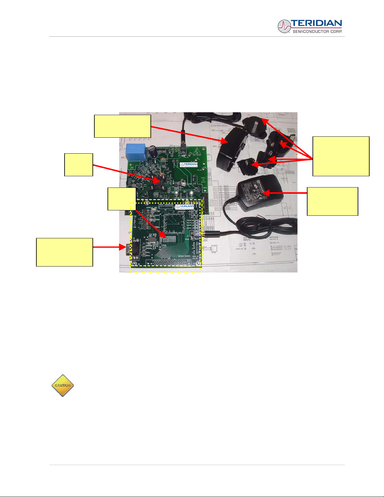
Figure 1-1 shows the basic connections of the Demo Board plus Debug Board with the external equipment.
Power supply for
Demo Board
Demo
Board
Debug
Board
Country-specific
plug adapters
(US, Europe,
UK, Australia)
Power supply
for Debug
Board
Serial
connection to
PC
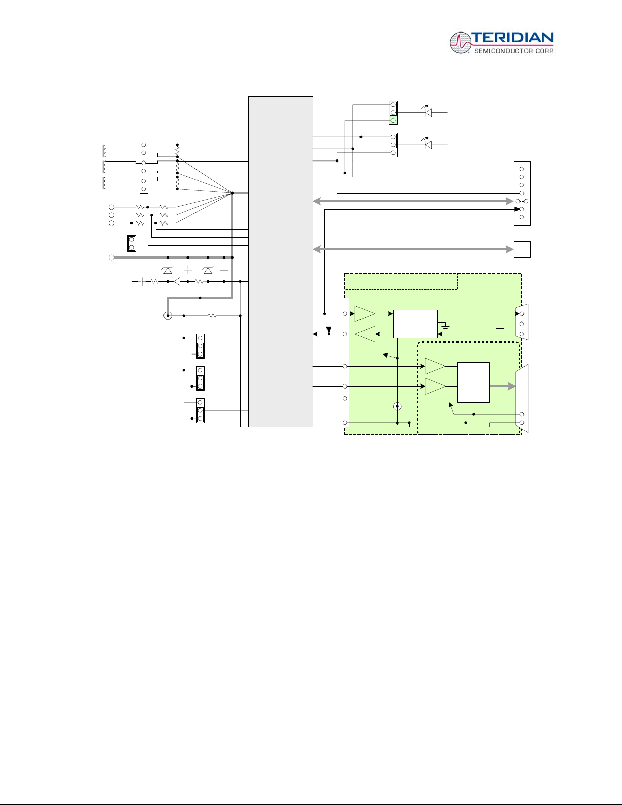
The 71M6515H demo board system is shown in Figure 1-2. It consists of a stand-alone rectangular meter
Demo Board and an optional Debug Board (most Debug Boards are partially assembled and have less
components than shown in Figure 1-2). The Demo Board contains all circuits necessary for operation as a
meter front end, calibration LEDs, and power supply. The Debug Board is optically isolated from the meter
and interfaces to a PC through a 9 pin serial port. For serial communication between the PC and the
TERIDIAN 71M6515H, the Debug Board needs to be plugged with its connector J3 into connector JP21 of
the Demo Board.
Connections to the external signals to be measured, i.e. scaled AC voltages and current signals derived
from shunt resistors or current transformers, are provided on the rear side of the demo board.
Note: It is recommended to set up the demo board with no live AC voltage connected, and to
connect live AC voltages only after the user is familiar with the demo system.
Figure 1-1: TERIDIAN 71M6515H Demo and Debug Boards: Basic Connections
Revision 2.0 8 of 66
© Copyright 2005 TERIDIAN Semiconductor Corporation
71M6515H Demo Board User’s Manual
DEMONSTRATION METER
External Current
Transformers
5V
DC
JP26
JP27
JP28
V3P3
3.3V
GND
S1
JP9
JP32
JP31
GND
IA
IB
IC
VC
VB
VA
JP25
NEUTRAL
JP24
JP23
JP22
JP1
71M6515H
Single-Chip Meter
AFE
WPULSE
IA
RPULSE
IB
IC
PULSE3
PULSE4
V3P3
VA
VB
VC
GND
TX
RX
UARTCSZ
TMUXOUT
BAUDRATE
CKTEST
PULSE_INIT
DEBUG BOARD (OPTIONAL)
OPTO
OPTO
OPTO SUPPLY
V5_DBG
5V DC
GND_DBG
JP21
JP30
JP29
DIO 0...8
SSI Signals
RS-232
INTERFACE
OPTO
OPTO
SUPPLY
D6
V3P3
D5
V3P3
OPTIONAL RTM
INTERFACE
OPTO
FPGA
V5_NI
External Interface
Connector
JP18
WPULSE
RPULSE
TX
RX
SSI Connector
JP6
DB9
to PC
COM Port
Figure 1-2: Block diagram for the TERIDIAN 71M6515H Demonstration Meter with Debug Board
Note: All input signals are referenced to the V3P3 (3.3V power supply to the chip).
1.6.1 POWER SUPPLY SETUP
There are several choices for meter power supply:
• Internal (using phase A of the AC line voltage). The internal power supply is only suitable when
phase A exceeds 220V RMS.
• External 5VDC connector (J1) on the Demo Board and external 5VDC connector (J1) on the Debug
Board.
The power supply jumper JP1 must be consistent with the power supply choice. JP1 disconnects phase A
from the power supply. This jumper should usually be left in place.
The internal supply is not strong enough to power the Debug Board. Thus, the external power supply should
always be used for the Debug Board, regardless whether the meter is powered by its internal supply or
through an external supply.
Revision 2.0 9 of 66
© Copyright 2005 TERIDIAN Semiconductor Corporation
71M6515H Demo Board User’s Manual
1.6.2 SERIAL CONNECTION SETUP
For connection of the DB9 serial port to a PC, either a straight or a so-called “null-modem” cable may be
used. JP1 and JP2 are plugged in for the straight cable, and JP3/JP4 are empty. The jumper configuration is
reversed for the null-modem cable, as shown in Table 1-1.
Configuration JP1 JP2 JP3 JP4
Straight Cable installed installed -- --
Null-Modem Cable -- -- installed installed
Table 1-1: Jumper settings on Debug Board
JP1 through JP4 can also be used to alter the connection when the PC is not configured as a DCE device.
Table 1-2 shows the connections necessary for the straight DB9 cable and the pin definitions.
PC Pin Function Demo Board Pin
2 TX 2
3 RX 3
5 Signal Ground 5
Table 1-2: Straight cable connections
Table 1-3 shows the connections necessary for the null-modem DB9 cable and the pin definitions.
PC Pin Function Demo Board Pin
2 TX 3
3 RX 2
5 Signal Ground 5
Table 1-3: Null-modem cable connections
1.7 PREPARING THE PC
The Control Program PMtest.exe must be copied from the CD-ROM to a directory on the host PC. The
program can then be started directly by double-clicking on the PMTest.exe icon (see Figure 1-3).
Figure 1-3: Control Program Icon
PMTest.exe can work in two baud rates and on any COM port. To configure PMTest.exe for the desired
operation mode, the original PMTest.exe file is copied to or renamed to a file with a name of the form:
PMTestxxxCy.exe
If xxx = 192, the program will operate at 19.2kb/s, if xxx = 384, the program will operate at 38.4kb/s (UART
speed when communicating with the 71M6515H).
The number substituted for y states the COM port number that the program is using for communicating with
the host.
Example: When named PMTest192C2.exe, the program will operate with 19.2kb/s via COM port 2.
PMTest.exe
Revision 2.0 10 of 66
© Copyright 2005 TERIDIAN Semiconductor Corporation

71M6515H Demo Board User’s Manual
Note: For smooth operation of the PMTest program it is important to observe the following rules:
• It is important to exit all programs that access COM port 1 before PMTEST.exe is started.
• Make sure all applicable updates to the Windows ® operating system are installed before running
the application.
• PMTest.exe will not run on Windows® 98 or older operating systems.
Real-time performance can be affected by processor-intense operations of the PC, such as starting new
applications, loading files into applications, or ending applications. Such operations have to be avoided to
ensure uninterrupted communication between PC and the 6515H Demo Board.
Do not press the ALT key on the keyboard!
1.8
1.8.1
1.8.2
USING THE DEMO BOARD
The 71M6515H Demo Board is a ready-to-use meter with a preprogrammed scaling factor Kh of 3.2
Wh/pulse. In order to be used with a calibrated load or a meter calibration system, the board should be
connected to the AC power source using the spade terminals on the bottom of the board. The current
transformers should be connected to the dual-pin headers on the bottom of the board. For the Kh to be
adjusted properly, current transformers with 2,000:1 winding ratio must be used.
STARTING UP THE DEMO BOARD AND THE GUI PROGRAM
In order to control and monitor the Demo Board, the connections specified in section 1.6 have to be
established.
The sequence of actions when powering up the Demo Board is as follows:
1. Power up the Demo Board
2. Start the GUI Control Program PMTest.exe.
3. Check for communication between the GUI Control Program and the 71M6515H. Communication is
established when the green “LED” indicator labeled 1SEC on the GUI screen flashes red every
second.
4. Initialize the 71M6515H to match the desired application and measurement parameters. Establish
the CE image, calibration factors, pulse parameters, nominal temperature, IMAX/VMAX using the
commands and fields described in 1.8.2.
5. Establish the desired configuration using the bits of the CONFIG register (field 16 in the GUI
window), but do not enable the CE.
6. Enable the CE by clicking the square button next to “CE_ENABLE”.
Once, voltage is applied and load current is flowing, the red LED D5 will flash each time an energy sum of
3.2 Wh is collected.
Similarly, the red LED D6 will flash each time a reactive energy sum of 3.2 VARh is collected.
CONTROLLING THE DEMO BOARD
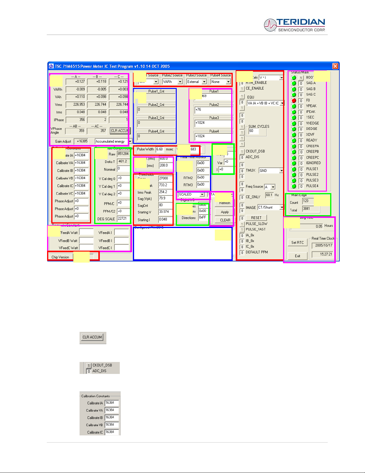
Upon starting the PMTEST.exe application, the graphical user interface (GUI) of the demo application
shown in Figure 1-4 will be displayed on the screen. The gray boxes are the meter outputs and the white
boxes contain host, i.e. user, inputs.
It is important to enable the computation engine (CE) in order to see activity in the GUI window. You can
check the computation engine (CE) status by verifying the status of the button on the left of CE_ENABLE in
the “Config” block of the GUI. It should display a “1”, as shown in Figure 1-4. If not, the CE can be enabled
by clicking the “0” button to the left of the “CE_ENABLE” text using the left mouse button. Upon clicking, the
“0” will toggle to a “1”, and the green and red indicator lights underneath the “Status/Mask” text will start
blinking.
Revision 2.0 11 of 66
© Copyright 2005 TERIDIAN Semiconductor Corporation
71M6515H Demo Board User’s Manual
GUI WINDOW - OVERVIEW 1.8.3
1
5
6
2
3
9
10
8
11
14
16
17
7
12
13
18
4
20
Figure 1-4: Host GUI Window w/ Functional Groups (Areas) Marked and Numbered
1.8.4 GUI WINDOW – DISPLAY AND CONTROL FIELDS
The PMTEST (GUI) window, as shown in Figure 1-4, contains a number of major blocks or areas (Pulse
Source Select, Config, Status/Mask, Calibration Constants, Temperature Compensation, Real-Time Monitor,
Digital I/O, Thresholds and Operating Time). These major blocks (labeled 1 through 12 in Figure 1-4) group
the functionally related buttons and fields together. The elements of the GUI are as follows:
• Rectangular buttons: Buttons that can be clicked by the user to initiate an action.
• Square buttons: Buttons that can be clicked by the user to initiate an action. The square buttons have
a single digit showing the current state of the signal. A “1” is on and a “0” is off.
• Entry fields: White rectangular fields that can be edited by the user. The delete key plus the number
and cursor keys work in this type of field.
19
15
Revision 2.0 12 of 66
© Copyright 2005 TERIDIAN Semiconductor Corporation

71M6515H Demo Board User’s Manual
• Display fields: Gray rectangular fields that indicate settings, measurements etc. of the 6515H chip.
These fields cannot be edited by the user.
• List fields: Entry fields that allow selection from the pre-determined list of choices once the down-
• Indicator lights: Red and green activity indicators underneath the “Status/Mask” label.
A summary of all of the GUI window areas follows on the next pages.
pointing arrow is pressed (“pull-down” menus).
Green lights mean no activity. Red lights mean that the corresponding bit in
the STATUS mask is set, i.e. the condition is true.
With an input signal (phase A, B, C voltage) present, the F0 light will be on
indicating that the square wave following the input signal is being
generated. The light at “1SEC” will blink red every second. Other lights will
stay green until the corresponding condition is true, e.g. when the input
signal meets a sag or over-voltage threshold.
Revision 2.0 13 of 66
© Copyright 2005 TERIDIAN Semiconductor Corporation
71M6515H Demo Board User’s Manual
1.8.5 GUI WINDOW CONTROL AND DISPLAY FIELDS – DETAILED DESCRIPTION
Energy, Voltage/Current and Phase Area (1):
This area is in the upper left corner of the GUI window and contains a number of display fields arranged in
columns. Phase A is the left column, phase B is the center column and phase C is the right column.
Next to the display fields in this area, there are a list field and a rectangular button controlling basic functions
of the Energy, Voltage/Current and Phase Area:
GUI Element (Label)
Element
Function
Type
Accumulated energy,
Instantaneous energy
List field
This control toggles the display of the Wh, VARh and VAh fields
from total accumulated energy to instantaneous energy, i.e.
energy per accumulation interval
CLR ACCUM
Rectangular
button
Resets the accumulators for Wh, VARh and VAh to zero. It also
resets the “Main Edge” counters in the Status/Mask area and the
pulse counters.
The function of the display fields depends on the selected mode, accumulated or instantaneous energy:
GUI Element (Label)
Wh
VARh
Function – Accumulated Energy
Selected
These fields display the accumulated
energy (real power x time) for each
phase.
These fields display the accumulated
reactive energy (reactive power x
Function – Instantaneous Energy
Selected
These fields display the energy (real
power x time) collected during the last
accumulation interval for each phase.
These fields display the reactive energy
(reactive power x time) for each phase.
time) for each phase.
VAh
These fields display the accumulated
apparent energy (apparent power x
time) for each phase.
These fields display the accumulated
apparent energy (apparent power x
time) collected during the last
accumulation interval for each phase.
Vrms These fields display the momentary voltages (RMS) for each phase.
Irms These fields display the momentary currents (RMS) for each phase.
Iphase These fields display the momentary phase angles of the currents for each phase.
VPhase angle
These fields display the momentary phase angles between the phases A and B
(underneath “--- AB ---“) and B and C (underneath “---BC---“).
Gain Adjust
This field displays the current value of the gain adjusted by the temperature
compensation mechanism. It is functionally associated with the fields in area 10.
When no compensation is active, or the temperature deviation is minimal, the
default value of 16384 will be displayed.
Revision 2.0 14 of 66
© Copyright 2005 TERIDIAN Semiconductor Corporation
71M6515H Demo Board User’s Manual
Calibration Constants Area (2):
This area is on the left side of the GUI window and contains three entry fields for each phase. The function
depends on the selected CE image (CT/Shunt or Rogowski sensor):
GUI Element
Function (CT/Shunt) Function (Rogowski Sensor)
(Label)
Calibrate IA Calibration constant for phase A current (default = 16384)
Calibrate VA Calibration constant for phase A voltage (default = 16384)
Calibrate IB Calibration constant for phase B current (default = 16384)
Calibrate VB Calibration constant for phase B voltage (default = 16384)
Calibrate IC Calibration constant for phase C current (default = 16384)
Calibrate VC Calibration constant for phase C voltage (default = 16384)
Phase Adjust A
Calibration constant for phase A current
angle (default = 0)
Phase Adjust B
Calibration constant for phase B current
angle (default = 0)
Phase Adjust C
Calibration constant for phase C current
angle (default = 0)
During calibration (see section 2.1), the values of the calibration coefficients obtained with the calibration
formulae should be entered in these fields.
Temperature Compensation Area (3):
This area consists of a vertical column of entry and display fields to the right of the Calibration Constants
area. The Gain Adjust field from area 1 functionally belongs in the Temperature Compensation area.
GUI Element
(Label)
Element
Type
Raw Display field -- Raw temperature (chip substrate temperature)
Delta T Display field --
Nominal Entry field 0
Y Cal deg 0 Entry field 0
Y Cal deg 1 Entry field 0
Y Cal deg 2 Entry field 0
PPM/C Entry field 0
PPM/C2 Entry field 0
DEG SCALE Entry field 22721
Default Function
Difference between raw and nominal (calibration)
temperature
The raw temperature should be entered here during
calibration
The constant correction coefficient for the RTC can be
entered here if RTC compensation is required.
The linear correction coefficient for the RTC can be entered
here if RTC compensation is required.
The quadratic correction coefficient for the RTC can be
entered here if RTC compensation is required.
The linear compensation coefficient of gain over
temperature is entered here automatically as soon as a
temperature value is entered in the “Nominal” field.
Values determined by the host may be entered here if
the DEFAULT PPM bit in the Configuration area is set to
0.
The quadratic compensation coefficient of gain over
temperature is entered here. See the PPM/C field for details.
Scaling factor for the calculation of temperature. The default
value for DEG SCALE (22721) should not be changed.
TEMP_X = DEGSCALE * 2
Calibration constant for phase A current
angle (default = -3973)
Calibration constant for phase B current
angle (default = -3973)
Calibration constant for phase C current
angle (default = -3973)
-22
* (TEMP_RAW - TEMP_NOM)
Revision 2.0 15 of 66
© Copyright 2005 TERIDIAN Semiconductor Corporation
71M6515H Demo Board User’s Manual
Rogowski Calibration Area (4):
This area consists of two vertical columns of entry fields in the lower left side of the window. The coefficients
are only active when the Rogowski image is selected for the CE.
GUI Element
(Label)
Default Function
VFeedA Watt 0 Calibration coefficient for phase A voltage feed through (default = 0)
VFeedB Watt 0 Calibration coefficient for phase B voltage feed through (default = 0)
VFeedC Watt 0 Calibration coefficient for phase C voltage feed through (default = 0)
VFeed A I 0 Not implemented
VFeed B I 0 Not implemented
VFeed C I 0 Not implemented
Pulse Source Selection Area (5):
This area consists of four list fields to the right of the Energy, Voltage/Current and Phase area. The entries
determine the configuration and settings of the two pulse outputs used for four-quadrant metering.
GUI Element
Default Function
(Label)
Pulse1 Source Wh
Pulse2 Source VARh
Pulse3 Source Wh
Pulse4 Source VARh
When external source is selected for any pulse generator, the missing pulse flags (PULSE1,
PULSE2, PULSE3, PULSE4) will be active for each accumulation interval for which the host does not
provide an input.
Pulse Count Area (6):
This area consists of a vertical column of display fields underneath the Pulse Source area.
GUI Element
Default Function
(Label)
PULSE1_Cnt 0 This field displays the count of pulses generated on the PULSEW output.
PULSE2_Cnt 0 This field displays the count of pulses generated on the PULSER output.
PULSE3_Cnt 0 This field displays the count of pulses generated on the PULSE3 output.
PULSE4_Cnt 0 This field displays the pulse count of pulses generated on the PULSE4.
Pressing the CLR ACCUM button in area 1 will reset the pulse counts to zero.
This list field allows selection of internal, external, or one of 35 postprocessed parameters as the source for the PULSEW output.
This list field allows selection of internal, external, or one of 35 postprocessed parameters as the source for the PULSER output.
This list field allows selection of either an external (host) input or one of 35
post-processed parameters as the source for the PULSE3 output. The
selection “none” is also available.
When “none” is selected, the pulse output is disabled.
This list field allows selection of either an external (host) input or one of 35
post-processed parameters as the source for the PULSE4 output. The
selection “none” is also available.
When “none” is selected, the pulse output is disabled.
Revision 2.0 16 of 66
© Copyright 2005 TERIDIAN Semiconductor Corporation
71M6515H Demo Board User’s Manual
External Pulse Control Area (7):
This area consists of a vertical column of combined display/entry fields to the right of the Pulse Count area.
A field can be made and entry field by selecting “External” for the corresponding pulse source in the Pulse
Source Selection area. In all other selections the fields are display fields.
When the corresponding Pulse Source selection in the Pulse Source Selection area is “External”, values
can be entered in the External Pulse Control fields to simulate pulse control by the host.
A new value must be entered in each new accumulation interval. The displayed values return to zero as
soon as the next accumulation interval starts and no new values are supplied by the host. If no values are
supplied by the host, the associated flags in the STATUS register (see STATUS/MASK area) will be set.
If very large numbers are entered, the pulses may be generated over several accumulation intervals.
When the corresponding Pulse Source selection in the Pulse Source Selection area is “Internal” or postprocessed values, the display fields of the External Pulse Control area contain input values N that
correspond to the pulse rate “f” per the equation:
f = WRATE * X * N * 35.82*10
In other words, the ADC count corresponding to the applied voltages at the Vn and In pins (VA/IA, VB/IB,
VC/IC) will be displayed.
GUI Element
(Label)
Pulse1 0 Host-provided pulse count for the PULSEW output.
Pulse2 0 Host-provided pulse count for the PULSER output.
Pulse3 0 Host-provided pulse count for the PULSE3 output.
Pulse4 0 Host-provided pulse count for the PULS4W output.
Pulse Width and Pulse Rate Control Area (8):
This area consists of two entry fields to the right of the Temperature Compensation area.
GUI Element
(Label)
WRATE 683
Pulse Width 6.68ms This field determines the pulse width in ms.
Default Function
Default Function
-12
This field, together with SUM_CYCLES, VMAX, IMAX and In8 determines
the Kh factor of the chip as follows:
8
=
Kh /5757.1
_
X is determined by the two fields PULSE_SLOW and PULSE_FAST in the
Configuration area.
InIMAXVMAX
XWRATECYCLESSUM
PulseWh
Revision 2.0 17 of 66
© Copyright 2005 TERIDIAN Semiconductor Corporation
71M6515H Demo Board User’s Manual
System Constants Area (9):
This area consists of two entry fields to the right of the Temperature Compensation area. Entries in these
fields determine the system parameters of the Demo Board.
GUI Element
(Label)
IMAX 208A
VMAX 600V
Warning Thresholds Area (10):
This area consists of seven entry fields to the right of the Temperature Compensation area.
GUI Element
(Label)
Creep 27000
Vrms Peak 733.2 Threshold for over-voltage alarms, measured in Vrms.
Irms Peak 254.2 Threshold for over-current alarms, measured in Arms.
Sag (Vpk) 79.9
SagCnt 80
Starting V 39.974
Starting I 0.048
Default Function
Default Function
IMAX is the RMS meter current that results in 250mV peak signal at the
ADC input. This variable reflects the scaling implemented by the voltage
sensing resistors of the Demo Board.
Note: When using shunt resistors as current sensors, IMAX must be
sh
ppmax
pp
⋅
= 250mV):
max
2
calculated as (V
V
IMAX
=
R
VMAX is the RMS meter voltage that results in 250mV peak signal at the
ADC input. This variable reflects the design of the current sensing circuitry
of the Demo Board, assuming a 2000:1 current transformer.
Determines the creep threshold. For each phase, if WSUM_X and
VARSUM_X of that phase are less than the value in the CREEP field, the
contents of I2h, Wh, and VARh for that phase will be set to zero for the
whole accumulation interval. If all phases are below the creep threshold,
the CREEP bit in the status word is set. The default value is 6000.
Determines the voltage sag threshold. The peak voltage must exceed
the voltage entered in this field at least once each SAG_CNT samples in
order to prevent a sag warning.
Values can be entered directly in Volts. The GUI will round the entered
value to the next possible value that can be represented with the
resolution used for this parameter.
Determines the sag alarm setting. Sag must persist SAG_CNT*397µs
before the sag alarm is generated. Allowed range is 1 to (215-1). Default
is 80 (31.7ms).
Determines the voltage below which the calculation of frequency, zero
crossings and voltage phase is suppressed.
Determines the current below which the calculation of current-related
values is suppressed.
Revision 2.0 18 of 66
© Copyright 2005 TERIDIAN Semiconductor Corporation
71M6515H Demo Board User’s Manual
Real-Time Monitor Area (11):
This area consists of four entry fields to the right of the System Constants area. The entries determine any
four CE data memory locations to be monitored. The RTM_ENABLE square button in the Configuration area
has to be in the “1” position for the RTM to be active.
GUI Element
Default Function
(Label)
RTM0 0x00 First CE data memory location to be monitored.
RTM1 0x00 Second CE data memory location to be monitored.
RTM2 0x00 Third CE data memory location to be monitored.
RTM3 0x00 Fourth CE data memory location to be monitored.
Note: Using the RTM interface requires special external hardware. Contact TERIDIAN for details.
QUANT Area (12):
This area consists of three entry fields that can be used to eliminate non-linearity at low currents caused by
truncation noise. The parameters entered here are closely related to the calibration parameters.
GUI Element
Default Function
(Label)
Watt 0 Noise compensation factor for the Watt calculation
VAR 0 Noise compensation factor for the VAR calculation
I 0 Noise compensation factor for the current calculation
Multi-Purpose Area (13):
This area consists of two list fields and three rectangular buttons.
GUI Element
(Label)
Element
Type
SCALED/RAW List field
STANDARD/
List field
HEX
Refresh
Rectangular
button
Apply
Rectangular
button
CLEAR
Rectangular
button
Function
This list field toggles the display of display and entry fields between
scaled (displayed values scaled using IMAX and VMAX) and raw
data (raw counts from 6515H) mode. In scaled mode, values for
voltage, current, and energy will be displayed as V, A, Wh, VARh etc.
In raw mode, the values will appear in the internal format of the
71M6515H chip.
This list field toggles the values shown in display and entry fields
between standard (decimal) and hexadecimal mode.
Pressing this button forces the GUI to transmit any changes made in
entry or list fields to the 71M6515H chip.
Placing the cursor into another entry field will have the same effect as
the Refresh button. Pressing this button will apply a change made in
an entry field.
Pressing this button will clear the contents of the Status Window.
Revision 2.0 19 of 66
© Copyright 2005 TERIDIAN Semiconductor Corporation
71M6515H Demo Board User’s Manual
Digital I/O Area (14):
This area consists of three entry fields below the Real-Time Monitor area. The entries determine the
configuration and settings of the eight DIO pins (D0 to D7).
GUI Element
Default Function
(Label)
Values 0x00
Interrupts 0x00
Direction 0xFF
A signal transition on an input pin will generate a DEDGE interrupt only once. This interrupt will not be synchronized with the accumulation interval or the 1-sec interrupt. Several transitions per accumulation interval
are possible.
With every signal transition on a DIO pin, the message “Some Dn pin values have changed!” will be
displayed in the Status Window.
Status Window Area (15):
This is the white, rectangular window at the bottom center of the GUI display. Activities of the PMtest.exe
GUI Control program, error messages etc. are listed here.
If more events occur than can be displayed in the lines of this window, the display will scroll. Events and
messages that occurred in the past will then be displayed by scrolling the window using the scroll arrows to
the right of it.
When the rectangular CLEAR button above the Status Window is pressed, the messages displayed in the
Status Window are deleted.
The hexadecimal number entered here defines the pattern that is applied
to the I/O pins.
The hexadecimal pattern entered in this field determines whether a
DEDGE interrupt is generated upon a bit changing its status. A 1 means
that the corresponding DIO pin generates an interrupt.
DEDGE interrupts are only generated for DIO pins that are configured
as inputs.
The hexadecimal number entered here defines whether I/O pins are inputs
(0) or outputs (1).
Revision 2.0 20 of 66
© Copyright 2005 TERIDIAN Semiconductor Corporation
 Loading...